ELECTRONICS DIVISION INTERNAL REPORT NO. 255 · PDF fileELECTRONICS DIVISION INTERNAL REPORT...
32
NATIONAL RADIO ASTRONOMY OBSERVATORY CHARLOTTESVILLE, VIRGINIA ELECTRONICS DIVISION INTERNAL REPORT NO. 255 A SYNTHESIZED, 90-120 GHz SIGNAL SOURCE J. W. ARCHER AND M, J. CRAWFORD, JR DECEMBER 1984 NUMBER OF COPIES: 150
Transcript of ELECTRONICS DIVISION INTERNAL REPORT NO. 255 · PDF fileELECTRONICS DIVISION INTERNAL REPORT...
NATIONAL RADIO ASTRONOMY OBSERVATORY
CHARLOTTESVILLE, VIRGINIA
ELECTRONICS DIVISION INTERNAL REPORT NO. 255
A SYNTHESIZED, 90-120 GHz SIGNAL SOURCE
J. W. ARCHER AND M, J. CRAWFORD, JR
DECEMBER 1984
NUMBER OF COPIES: 150
A SYNTHESIZED 90-120 GHZ SIGNAL SOURCE
J. W. Archer and M. J. Crawford, Jr.
Table of Contents
I. Introduction 1 II. The 26.5-40 GHz Frequency Synthesizer 2
A. General Description 2 B. Design of the UHF Synthesizers 5 C. The Coarse Tuning and Bias Modulation Amplifiers 11 D. The Main 26.5-40 GHz Phase Lock Loop 14
III. The 90-120 GHz Frequency Tripler 21 IV. The Complete Synthesized L0 Source 27 V. Summary 27 VI. Acknowledgements 28
Figures
Figure 1 26.5-40 GHz Synthesizer Block Diagram 3 Figure 2 0.88-1.32 GHz Synthesizer Schematic 7 Figure 3 ROM and 9*8 Complement Encoder Schematic 9 Figure 4(a) Spectrum of 1.76-2.64 GHz Synthesizer Output 10
(b) Spectrum of 1.76-2.64 GHz Synthesizer Output 10 (c) 400-500 MHz Reference Signal Spectrum 12 (d) I. F. Spectrum in Main Loop 12
Figure 5 Tuning Coil Driver Schematic 13 Figure 6 Harmonic Mixer Triplexer Schematic 15 Figure 7 Sweep Generator Schematic 18 Figure 8 FM Coil Driver and Loop Amplifier Schematic 20 Figure 9(a) Tripler Block: Cross-Sectional View 22 Figure 9(b) Tripler Block: Cross-Sectional View 23 Figure 10 Output Power vs Output Frequency for Tripler
Alone and for Complete Signal Source 25 Figure 11 Tripler Conversion Efficiency vs Input Power 26
References 29
A SYNTHESIZED 90-120 GHZ SIGNAL SOURCE
J. W. Archer and M. J. Crawford, Jr.
I. Introduction
The advantages of all-solid-state millimeter wavelength receivers have
been clear to system designers for many years. Substantial savings in cost
and weight, and significantly enhanced system reliability, can be achieved with
a completely solid-state design. Until recently, achieving a widely tuneable
solid-state local oscillator system has proven to be a significant obstacle
to the development of broadband heterodyne receiver systems of this type.
Developments in millimeter wave harmonic generator design [1],[2], Gunn oscillator
technology [1],[3] and the reduction in the L0 power requirements for heterodyne
receivers through the use of improved, cooled Schottky diode [4],[5] or super¬
conducting mixer [6],[7] elements have now made it feasible to realise practical
receivers with solid state LO's. In many applications, frequency and/or phase
stability of the L0 source is of prime importance. The construction of a highly
stable, widely tuneable synthesizer [8], such as described here, is therefore
a significant development.
The following sections of this paper will describe the design and construction
of the 26.5-40 GHz frequency synthesizer. Performance data will be given, which
illustrate the frequency stability, output power and spectral purity of the
phase locked source. The design of the frequency tripler is then described
and performance curves are given. Finally, data is presented showing the performance
of the complete synthesized LO source.
II. The 26.5-40 GHz Frequency Synthesizer
A. General Description:
The principal millimeter wavelength signal source in the LO system is a
YIG tuned GaAs Gunn oscillator manufactured by Watkins Johnson, Inc. (Model
WJ-5610-302F). This oscillator may be electronically tuned between 26.5 and
40 GHz by varying the magnetic field applied to a spherical YIG resonator to
which the Gunn diode is coupled. The magnetic field is produced by current
flowing in the coils of an electromagnet, whose pole pieces enclose the YIG
element. As the tuning coil current is varied linearly from 660 mA to 1015
mA, the oscillator frequency varies in a smooth, almost linear response from
26.5 to 40 GHz. The peak deviation from linearity is about -60 MHz near the
upper and lower tuning limits. The tuning coil resistance is about 10 ohms
with an inductance of 160 mH. Another electromagnetic circuit is provided to
enable fine tuning of the oscillator frequency. This coil gives a sensitivity
of 125 kHz/mA with a maximum current of ± 800 mA, resulting in a peak attainable
deviation of + 100 MHz. In order to achieve the flattest output power response
as the output frequency is varied, the supply voltage to the Gunn diode must
be changed linearly and in synchronism with the tuning coil current - at 26.5
GHz the optimum Gunn bias is 5.2 volts and at 40 GHz the optimum bias is 3.4
volts. When the bias voltage is controlled in this manner, the output power
over the full tuning range is +13 dBm ± 1 dB.
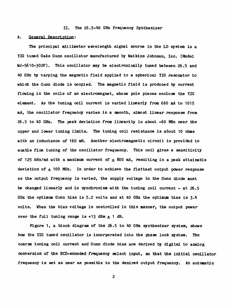
Figure 1, a block diagram of the 26.5 to 40 GHz synthesizer system, shows
how the YIG tuned oscillator is incorporated into the phase lock system. The
coarse tuning coil current and Gunn diode bias are derived by digital to analog
conversion of the BCD-encoded frequency select input, so that the initial oscillator
frequency is set as near as possible to the desired output frequency. An automatic
BCD CODE FRBQSET
COARSE TUNE D/A CONV
m O'S COMP A 3UBT 4
/ d 9'S COMP -10DB
VCO
EMF VTO-4B
TUNING COIL DRIVER
-100B r+l^-A
—1 PHASE/FREQ DET 1U /r-^^V
-^N KS PWR DIV
YIG OSCILLATOR WJ-5610-302F
ISOLATOR-
200B COUPLER-
rwi
LOOP FILTER
BPF 2200/800
■^N
BPF 450/100
PWR DIV
'^Xj L—/o, 1<— VC0
^"^1 P V ^ J AVANTEK 8041 LOOP FILTER \ /
y—vK ^— ^ \ 7 -10DB
LIM AMP WJ-CLA7
^ ^ PHASE DET f^-' MCL-ZFM4
10MHZ XCO
QUAD HYBRID
..PWR AMP MCL-ZFL2000 LOOP FILTER
BPF 2200/800 ^^ COSPLER
450/100
HARMONIC MIXER HP-11517A
V
LPF 500 IF AMP P-^ WJ-6200618
DC BIAS IN IF MONITOR
-10DB LIM AMP WJ-CLA7
26.5-40 GHZ OUT
LOCK INDICATOR
Fig. 1. A block diagram of the complete 26.5-40 GHz synthesizer system. A detailed description of the block diagram is given in the text, along with information on the design and operation of the individual system building blocks.
fine frequency sweep signal can be injected at the input of the coarse tuning
coil bias amplifier in order to tune the oscillator close enough to the desired
frequency for lock acquisition. The microwave output from the YIG oscillator
is fed through a broadband waveguide isolator and then sampled by a 20 dB cross-
guide coupler. The sampled signal is fed to a harmonic mixer (Hewlett-Packard
Model 11517A) where it is mixed with the 15th harmonic of a 1.76-2.64 GHz reference
signal. This signal is generated by extracting the second harmonic of the output
of one of two UHF frequency synthesizers in the system, both of which are locked
to a common, highly stable, 10 MHz reference signal. The frequency of the 2 GHz
reference is controlled by the first three digits of the frequency select input
data. Decimal 4 is subtracted from this number to correct for the 400 MHz offset
of the IF reference synthesizer and its S's complement code generated, in order
to derive the required preset data to determine the division modulus for the
programmable divider in the UHF synthesizer. A numerical example will help
in understanding the relationships:
Let the selected frequency be t31.6i t543j GHz (no special significance).
The division modulus will be 316 - 4 = 312. The output frequency from the UHF
synthesizer will be (10 MHz/12) x 312 x 4 = 1040 MHz. Its second harmonic component,
which is fed to the harmonic mixer, will be 2080 MHz. When the YIG oscillator
is tuned to the desired frequency, the IF output frequency from the harmonic
mixer will be 31,654.3 - 15 x 2080 = 454.3 MHz.
The IF output from the harmonic mixer is amplified and fed to a phase detector
where it is correlated with a signal derived from the second UHF synthesizer.
The frequency of the second synthesizer is controlled by the remaining three
digits of the frequency select command and incorporates a fixed frequency offset
of 400 MHz. Thus, in the example above the output frequency would be
400 + 54.3 = 454.3 MHz, which is exactly the required frequency if the YIG tuned
oscillator is to lock at 31.6543 GHz. The output of the phase detector is filtered,
amplified and fed back to control the phase of the YIG oscillator via the bias
applied to the fine tuning (FM) coil.
The use of separate synthesizers for coarse and fine control of the reference
frequencies is essential if acceptable phase noise is to be achieved in the
spectrum of the locked millimeter wave oscillator. The phase noise of the output
signal, within a loop bandwidth separation from the carrier, will be determined
primarily by the phase noise characteristics of the harmonic mixer reference
signal. If only the 1.76-2.64 GHz reference is made variable and the other
reference is fixed at, say, 400 MHz, it would be necessary to operate the phase
detector at 833 Hz in the remaining synthesizer to achieve a 100 KHz increment
in the millimeter wave output signal. Since the carrier-to-noise ratio for
phase noise degrades as the square of the frequency ratio, the FM noise
characteristics of the primary reference oscillator would be degraded by about
70 dB in the final output spectrum - clearly an unacceptable situation for practical
oscillators. By controlling the frequency of both reference signals and carrying
out fine frequency adjustment using an IF frequency offset, the phase noise
degradation is reduced to about 40 dB, which is acceptable when a high quality
10 MHz reference oscillator is employed.
B. Design of the UHF Synthesizers:
The 1.76-2.64 GHz and 400-500 MHz synthesizers are very similar in design,
using essentially the same digital circuitry for prescaling, variable modulus
division and phase/frequency detection. The significant differences are the
different reference frequencies (833 kHz vs 25 kHz), the number of variable
modulus counter stages (3 vs 4) and the manner in which the frequency select
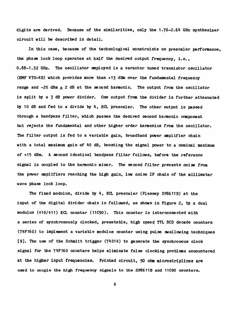
digits are derived. Because of the similarities, only the 1.76-2.64 GHz synthesizer
circuit will be described in detail.
In this case, because of the technological constraints on prescaler performance,
the phase lock loop operates at half the desired output frequency, i.e.,
0.88-1.32 GHz. The oscillator employed is a varactor tuned transistor oscillator
(EMF VT0-4B) which provides more than +13 dBm over the fundamental frequency
range and -25 dBm ± 2 dB at the second harmonic. The output from the oscillator
is split by a 3 dB power divider. One output from the divider is further attenuated
by 10 dB and fed to a divide by 4, ECL prescaler. The other output is passed
through a bandpass filter, which passes the desired second harmonic component
but rejects the fundamental and other higher order harmonics from the oscillator.
The filter output is fed to a variable gain, broadband power amplifier chain
with a total maximum gain of 40 dB, boosting the signal power to a nominal maximum
of +15 dBm. A second identical bandpass filter follows, before the reference
signal is coupled to the harmonic mixer. The second filter prevents noise from
the power amplifiers reaching the high gain, low noise IF chain of the millimeter
wave phase lock loop.
The fixed modulus, divide by 4, ECL prescaler (Plessey SP8611B) at the
input of the digital divider chain is followed, as shown in Figure 2, by a dual
modulus (-M0/-M1) ECL counter (11C90). This counter is interconnected with
a series of synchronously clocked, presetable, high speed TTL BCD decade counters
(74F160) to implement a variable modulus counter using pulse swallowing techniques
[9]. The use of the Schmitt trigger (74S14) to generate the synchronous clock
signal for the 74F160 counters helps eliminate false clocking problems encountered
at the higher input frequencies. Printed circuit, 50 ohm microstriplines are
used to couple the high frequency signals to the SP8611B and 11C90 counters.
TO VARACTOR
I 47Q -N LOCK -^Hr-q) |ND|CAToR
—*<IOK^ I Asv
—^^415 TN9I4 *"
FROM VCO
10 MHZ H)
9s COMPLEMENT OF BCD
Fig. 2. A detailed circuit diagram of the 0.88-1.32 GHz digital frequency synthesizer. The 1.76-2.64 GHz reference signal fed to the millimeter wave harmonic mixer is obtained by filtering and amplifying the second harmonic of the VCO output signal.
The coupling and bypass capacitors are chip capacitors. The bypass capacitors
are grounded to the ground plane of the board using low inductance, plated-through
holes.
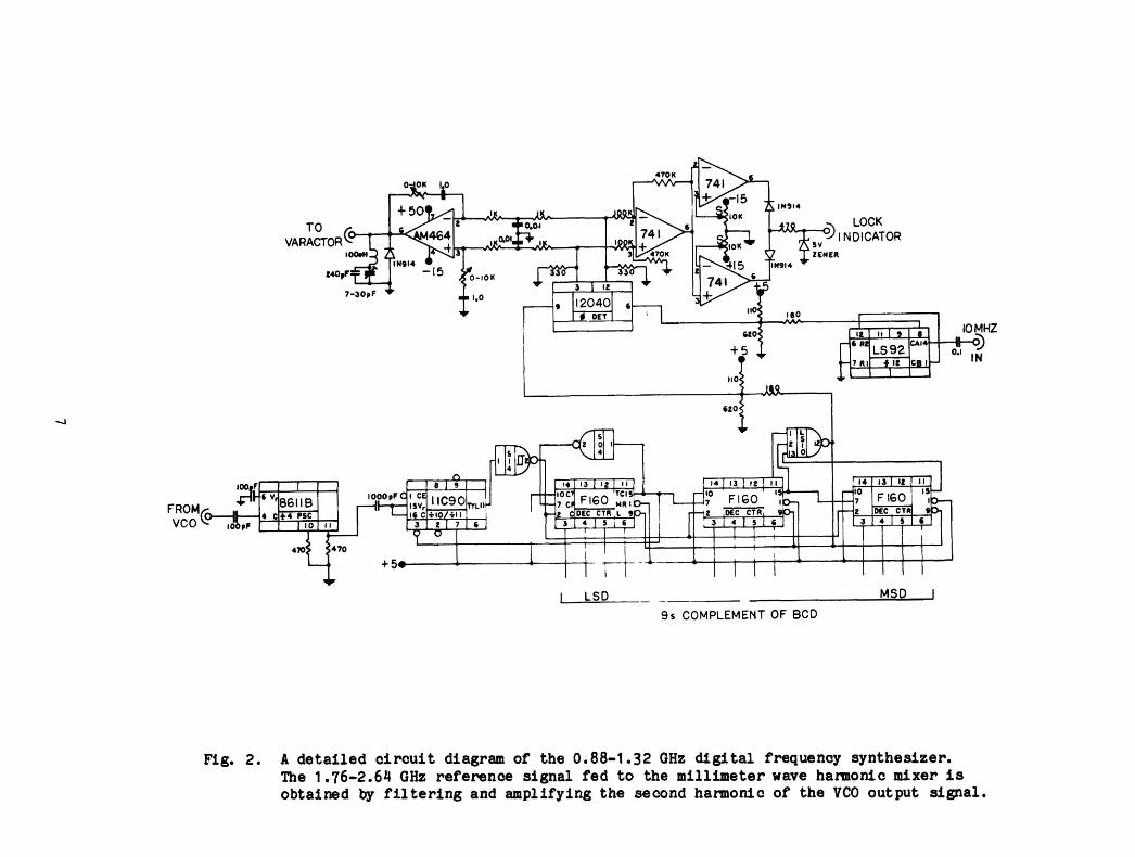
The division modulus preset digits to the programmable counters are derived
using 9ts complement encoders; one channel is illustrated in Figure 3. The
subtract decimal 4 function is performed prior to 9's complement encoding using
a look-up table stored in a set of read only memories. The complete circuit
and table are given in Figure 3- The output signal from the programmable divider
is fed, via a level translating resistor network, to an ECL phase frequency
detector (12040). The 833 kHz reference input for the detector is derived from
the 10 MHz standard using a divide by twelve, 74LS92 counter. The output pulses
from the phase detector are coupled to an active second order loop filter/integrator
with adjustable damping controls. An AM-464 (Analog Devices) operational amplifier
is used, which is capable of handling the high voltages required to directly
bias the tuning varactor in the VCO for complete coverage of the oscillator
tuning range. A common problem with a loop of this type is the appearance of
spurious components in the spectrum of the locked oscillator spaced at harmonics
of 833 kHz from the desired output frequency. These arise because of insufficient
filtering of the sharp output pulses from the phase/frequency detector at the
varactor bias output. In the present design, with a loop natural frequency
of about 20 kHz [10], RC pulse prefiltering (0.01 \iF capacitors in the input
resistor network) and a series resonant LC trap at the op-amp output are used
to reduce the amplitude of the spurious signals to acceptable levels. Photographs
of the typical output spectrum (at 2 GHz) from the 1.76-2.64 GHz synthesizer,
shown in Figures 4(a) and 4(b), demonstrate that the unwanted components are
at least 60 dB below the carrier. A simple lock indicator circuit is implemented
8
HP^f^r1
_ 9s COMPLEMENT OF BCD
DB> LSD
Fig. 3. A diagram showing the design of the SCI) subtract four, ROM circuit and the BCD to n9,s complement of BCD,,
converter. The inset table gives the logic used in implementing the look-up table stored in ROM.
SUBTRACT 4 PROM TABLE
Hex Address LSD ROM Other Two ROMS^
B 8 4 2 B 8 4 2
0 1 1 0 0 0 1 1 1 1 1 0 0 0 0 1 1 0 2 1 0 1 0 1 0 3 1 0 1 0 0 1 0 0 4 0 1 1 0 0 1 5 0 1 1 0 0 0 1 0 6 0 1 0 0 0 0 7 0 1 0 0 0 0 0 0 8 0 1 0 1 0 0 1 1
OF 10 11 12 13 14 15 16 17 18 19
1 0 1 0 0 1 0 1 0 0 0 0 0 0 0 0 1 0 0 1 0 0 0 0 0 0 0 0
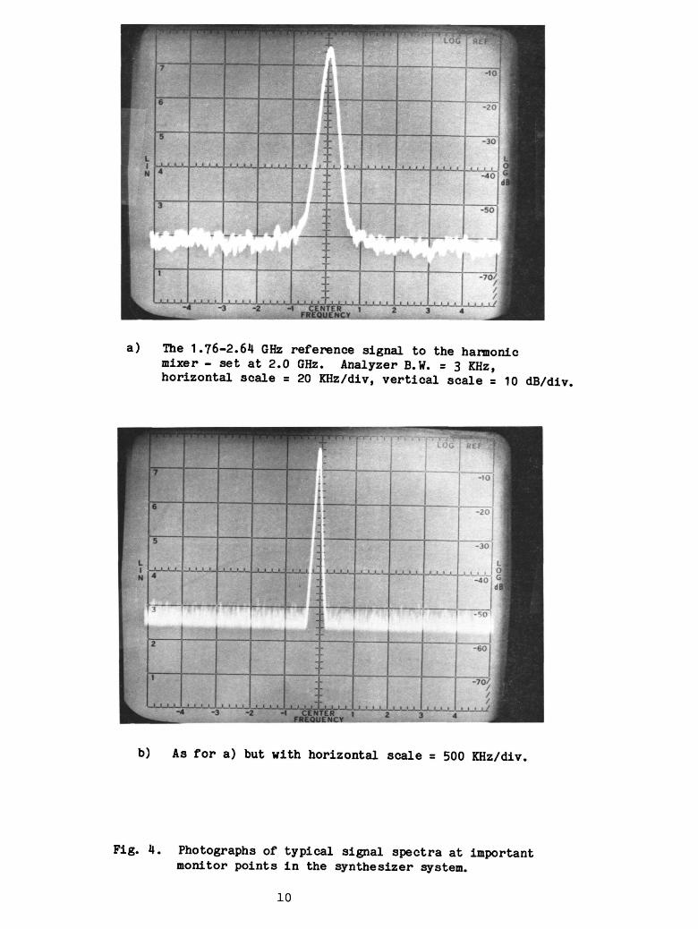
a) The 1.76-2.64 GHz reference signal to the harmonic mixer - set at 2.0 GHz. Analyzer B.W. =3 KHz, horizontal scale = 20 KHz/div, vertical scale = 10 dB/div,
b) As for a) but with horizontal scale = 500 KHz/div,
Fig. 4. Photographs of typical signal spectra at important monitor points in the synthesizer system.
10
using a differential amplifier to detect the presence of a frequency correction
signal from the 12040, followed by a dual threshold comparator which gives a
5 volt output signal when the loop is unlocked.
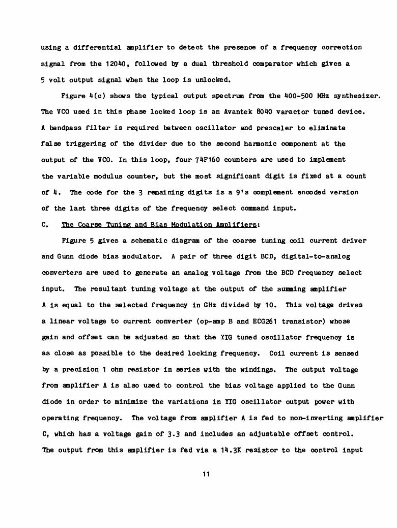
Figure 4(c) shows the typical output spectrum from the 400-500 MHz synthesizer.
The VCO used in this phase locked loop is an Avantek 8040 varactor tuned device.
A bandpass filter is required between oscillator and prescaler to eliminate
false triggering of the divider due to the second harmonic component at the
output of the VCO. In this loop, four 74F160 counters are used to implement
the variable modulus counter, but the most significant digit is fixed at a count
of 4. The code for the 3 remaining digits is a 91s complement encoded version
of the last three digits of the frequency select command input.
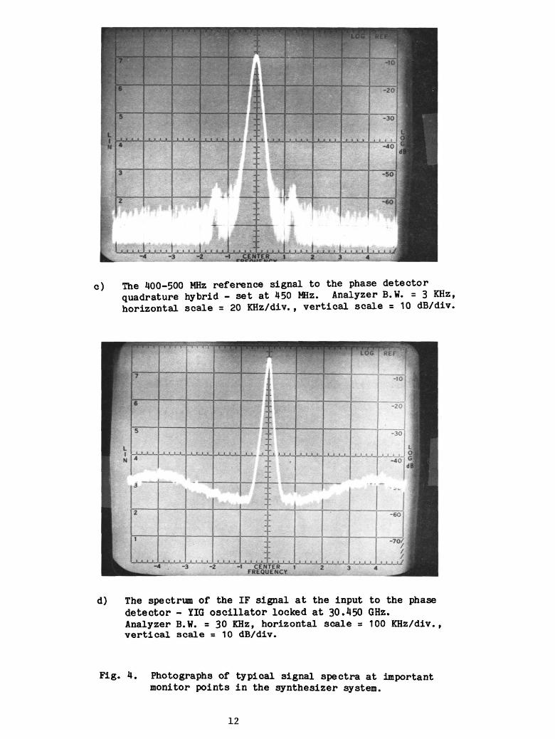
C. The Coarse Tuning and Bias Modulation Amplifiers:
Figure 5 gives a schematic diagram of the coarse tuning coil current driver
and Gunn diode bias modulator. A pair of three digit BCD, digital-to-analog
converters are used to generate an analog voltage from the BCD frequency select
input. The resultant tuning voltage at the output of the summing amplifier
A is equal to the selected frequency in GHz divided by 10. This voltage drives
a linear voltage to current converter (op-amp B and ECG261 transistor) whose
gain and offset can be adjusted so that the YIG tuned oscillator frequency is
as close as possible to the desired locking frequency. Coil current is sensed
by a precision 1 ohm resistor in series with the windings. The output voltage
from amplifier A is also used to control the bias voltage applied to the Gunn
diode in order to minimize the variations in YIG oscillator output power with
operating frequency. The voltage from amplifier A is fed to non-inverting amplifier
C, which has a voltage gain of 3-3 and includes an adjustable offset control.
The output from this amplifier is fed via a 14.3K resistor to the control input
11
c) The 400-500 MHz reference signal to the phase detector quadrature hybrid - set at 450 MHz. Analyzer B.W. =3 KHz, horizontal scale = 20 KHz/div., vertical scale = 10 dB/div.
d) The spectrum of the IF signal at the input to the phase detector - YIG oscillator locked at 30.450 GHz. Analyzer B.W. = 30 KHz, horizontal scale = 100 KHz/div., vertical scale =10 dB/div.
Fig. 4. Photographs of typical signal spectra at important monitor points in the synthesizer system.
12
BC5 CODE
IOOK 50K IOOK
+ 15 -15
MSD
LSD =
+ 15-15 +
TO TUNING COlLUa-i.oi A)
TO
KNEI£ GUNN
DIODE (&2-3^V)
15
Fig. 5. A schematic diagram of the coarse tuning coil driver circuit showing the D/A converter, driver amplifier and Gunn diode bias modulator.
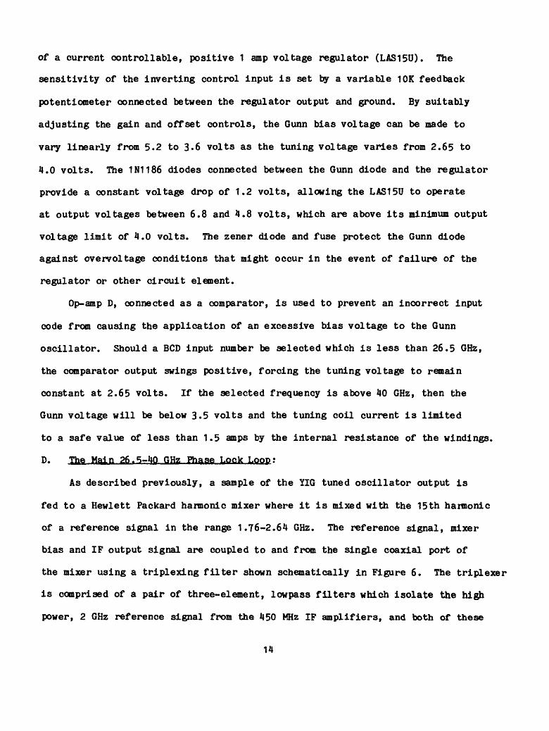
of a current controllable, positive 1 amp voltage regulator (LAS15U). The
sensitivity of the inverting control input is set by a variable 10K feedback
potentiometer connected between the regulator output and ground. By suitably
adjusting the gain and offset controls, the Gunn bias voltage can be made to
vary linearly from 5.2 to 3.6 volts as the tuning voltage varies from 2.65 to
4.0 volts. The IN1186 diodes connected between the Gunn diode and the regulator
provide a constant voltage drop of 1.2 volts, allowing the LAS15U to operate
at output voltages between 6.8 and 4.8 volts, which are above its minimum output
voltage limit of 4.0 volts. The zener diode and fuse protect the Gunn diode
against overvoltage conditions that might occur in the event of failure of the
regulator or other circuit element.
Op-amp D, connected as a comparator, is used to prevent an incorrect input
code from causing the application of an excessive bias voltage to the Gunn
oscillator. Should a BCD input number be selected which is less than 26.5 GHz,
the comparator output swings positive, forcing the tuning voltage to remain
constant at 2.65 volts. If the selected frequency is above 40 GHz, then the
Gunn voltage will be below 3-5 volts and the tuning coil current is limited
to a safe value of less than 1.5 amps by the internal resistance of the windings.
D. The Main 26.5-40 GHz Phase Lock LOOP:
As described previously, a sample of the YIG tuned oscillator output is
fed to a Hewlett Packard harmonic mixer where it is mixed with the 15th harmonic
of a reference signal in the range 1.76-2.64 GHz. The reference signal, mixer
bias and IF output signal are coupled to and from the single coaxial port of
the mixer using a triplexing filter shown schematically in Figure 6. The triplexer
is comprised of a pair of three-element, lowpass filters which isolate the high
power, 2 GHz reference signal from the 450 MHz IF amplifiers, and both of these
14
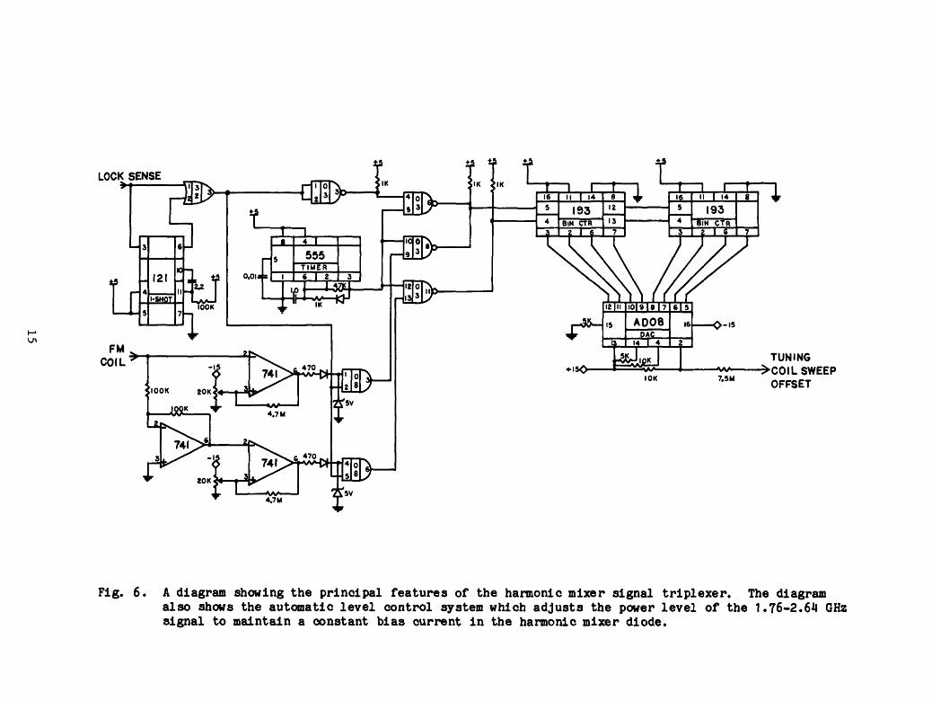
LOCK SENSE
COIL TUNING ** >C0IL SWEEP
OFFSET
Fig. 6. A diagram showing the principal features of the harmonic mixer signal triplexer. The diagram also shows the automatic level control system which adjusts the power level of the 1.76-2.64 GHz signal to maintain a constant bias current in the harmonic mixer diode.
signals in turn from the mixer DC bias input. DC blocking capacitors are provided
at the RF and IF ports. The triplexing filter was fabricated using microstripline
techniques on aluminum-backed, Teflon fiberglass dielectric material.
The harmonic mixer, which has widely varying sensitivity over the range
1.76-2.64 GHz, is operated in a zero voltage bias mode at a constant forward
current of 4.8 mA. The bias current is held constant by adjusting the power
of the 2 GHz input using a servo loop (shown in Figure 6), which controls the
gain of the reference signal power amplifier. Operation at a constant bias
current ensures a more uniform sensitivity for the harmonic mixer between 26.5
and 40 GHz and reduces variations in the IF power at the phase detector.
The 400-500 MHz IF output from the triplexer is passed to a lowpass filter
(500 MHz cutoff), which further attenuates the 2 GHz reference signal, before
being fed to a lew noise, high gain amplifier (3 dB NF, 45 dB gain). The first
amplifier is followed by a 400-500 MHz bandpass filter, a monitor directional
coupler, a limiting amplifier and a 10 dB attenuator, resulting in a nominal
input power to the phase detector power divider of +3 dBm. The reference signals
for the two double balanced mixer phase detectors are derived from the amplified
400-500 MHz synthesizer output using a quadrature hybrid. Nominal input power
to the hybrid is +3 dBm.
In order for the loop to be able to acquire lock, the difference frequency
between the IF signal from the hannonic mixer and the phase detector reference
signal must be less than the bandwidth of the loop filter (about 500 KHz).
This will not be the case when the YIG oscillator frequency is preset by the
coarse tuning coil because of the deviation of the tuning current vs frequency
response from linearity. Nevertheless, the difference frequency should be less
than 60 MHz for the oscillator used here. Provision is made in the design of
16
the coarse tuning coil driver amplifier for the injection of a small sweep offset
voltage, which can be used to bring the YIG oscillator frequency within the
lock range of the loop.
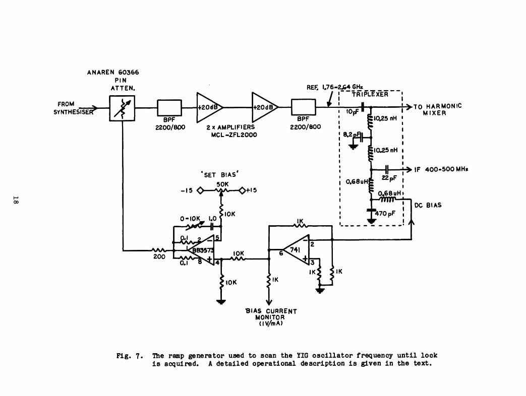
The sweep circuit is illustrated in Figure 7. The sweep function is implemented
digitally, a technique which has significant advantages over an analog method.
A 256 Hz clock pulse generated by a 555 timer is fed via a control gate to a
cascade of two 74LS193 binary up/down counters. The counter outputs are coupled
to an eight-bit D/A converter, which generates a repetitive voltage ramp as
the counters are clocked. The voltage ramp is fed via an appropriate scaling
resistor to the input of the coarse tuning coil driver amplifier, resulting
in a modulation of the YIG oscillator frequency by about + 100 MHz in synchronism
with the sweep voltage. When the YIG oscillator frequency comes within the
capture range of the loop (about 1 MHz) and lock is acquired, a voltage comparator
connected to the output of the quadrature phase detector senses the locked condition
and generates a +5 volt signal which disables the clock to the sweep counters.
The coarse tuning bias is thus latched at the condition at which lock was acquired.
A problem that has been encountered with the YIG oscillator used here is
significant frequency vs temperature dependence. In operation, after the loop
is locked, ambient temperature changes can cause the oscillator to drift out
of the range of the loop correction signal. A simple addition to the sweep
circuit has enabled this problem to be overcome. As shown in Figure 7, the
current in the YIG oscillator FM coil is converted to a suitable proportional
voltage and sensed by a dual threshold comparator with hysteresis, which is
triggered should the correction voltage exceed ± 2 volts (available range is
± 4 volts at a sensitivity of 0.1V/A). The comparator outputs control gates
which feed the clock signals to the up or down clock inputs of the binary counter
17
00
ANAREN 60366 PIN
ATTEN.
FROM SYNTHESISEIT
2200/800 2 x AMPLIFIERS MCL-ZFL2000
'SET BIAS* 50K
-is O—^K^—0+l5
-OK iAl0K 0-IOK LO
■AAA. f 1<PB357] 200
REF. L76-2J64GH* / '""TRIPLEXER"
lL1—fr BPF
2200/800
IK AAArf-
BIAS CURRENT MONITOR
(IV/mA)
>T0 HARMONIC MIXER
> IF 400-500 MHt
! ><
DC BIAS
Fig. 7. The ramp generator used to scan the YIG oscillator frequency until lock is acquired. A detailed operational description is given in the text.
cascade: If the FM coil current exceeds the threshold level, the clock is applied
to the counters in such a way as to change the coarse tuning voltage to result
in a reduction of FM coil current magnitude. A 0.5 volt hysteresis for the
comparator thresholds provides an overcorrection safety margin.
The FM coil driver and loop filter functions are combined in a single circuit,
shown in Figure 8. An LH0022 FET input op-amp is used in conjunction with a
diode biassed, complimentary-darlington connected, transistor power amplifier
to implement the FM coil driver, voltage to current converter circuit. This
configuration is capable of delivering currents of ± 0.8 A to bias the FM coil,
with current limiting provided by 0.5 ohm emitter resistors at ± 1.0 A. Coil
current is sensed by a precision 10 ohm resistor in series with the ground side
of the coil. When connected as an amplifier with a gain of 10 V/A (feedback
capacitor and damping resistor replaced with 10K) the amplifier small signal
bandwidth is greater than 1 MHz and crossover distortion is undetectable at
the output for a 5 volt peak to peak sinusoid at the input, for frequencies
below 50 KHz. When configured as an integrator for the loop filter function,
the 0.01 |iF feedback capacitor and 10K input resistor result in a loop natural
frequency of about 150 KHz (phase detector sensitivity, K. = 0.25 V/rad, oscillator
sensitivity, K0 r 7.85 x 10⁵ rad/sec/mA). As can be seen from Figure 8, the
feedback capacitor and damping resistor are shunted by an 18M resistor. Limiting
the DC gain (to 1800) in this manner aids in lock acquisition by keeping the
coil driver amplifier from latching in a current limiting state with the loop
in the unlocked condition. The 0.18 sec time constant introduced by the extra
gain limiting resistor in the feedback path does not significantly affect the
behaviour of the loop. An offset trim control is provided at the op-amp in
19
o
+ 15
0-10£ 0.01
FROM PHASE
DETECTOR 2.2K,
0-20K
:3K 2N3439
ALL DIODES IN9I4
2-2Kl HWn * 0.022
-I-
H 3K
DIODES 1-4 ON COMMON HEATS INK WITH D44/b45
TO FM COIL I (±0.8 A)
MM54I6
0-20K
04508
-15
Fig. 8. The circuit diagram of the FM coil driver amplifier which incorporates the loop filter for the YIG oscillator phase locked loop.
order to allow compensation for the DC offset associated with the balanced mixer
phase detector.
Figure 4(d) shows the spectrum of the IF signal measured at the IF monitor
coupler output with the YIG oscillator phase locked at 30.4500 GHz. The spectrum
is free of spurious non-harmonically related components to at least 30 dB below
the carrier. The noise sidebands characteristic of a spectrum from a phase
locked oscillator with a 3 dB loop bandwidth of about 400 KHz are clearly seen.
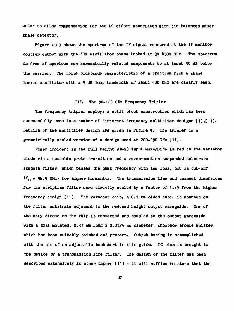
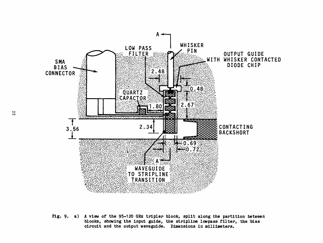
III. The 90-120 GHz Frequency Tripler
The frequency tripler employs a split block construction which has been
successfully used in a number of different frequency multiplier designs [1],[11].
Details of the multiplier design are given in Figure 9* The tripler is a
geometrically scaled version of a design used at 200-290 GHz [11].
Power incident in the full height WR-28 input waveguide is fed to the varactor
diode via a tuneable probe transition and a seven-section suspended substrate
lowpass filter, which passes the pump frequency with low loss, but is cut-off
(fc = 56.5 GHz) for higher harmonics. The transmission line and channel dimensions
for the stripline filter were directly scaled by a factor of 1.89 from the higher
frequency design [11]. The varactor chip, a 0.1 mm sided cube, is mounted on
the filter substrate adjacent to the reduced height output waveguide. One of
the many diodes on the chip is contacted and coupled to the output waveguide
with a post mounted, 0.31 mm long x 0.0125 mm diameter, phosphor bronze whisker,
which has been suitably pointed and prebent. Output tuning is accomplished
with the aid of an adjustable backshort in this guide. DC bias is brought to
the device by a transmission line filter. The design of the filter has been
described extensively in other papers [11] - it will suffice to state that the
21
N5
SMA BIAS
CONNECTOR
3.56
LOW PASS FILTER
SKER PIN
•■•ii
OUTPUT GUIDE WITH WHISKER CONTACTED
DIODE CHIP
QUARTZ ) :CAPACT0R?lP/3
CONTACTING BACKSHORT
Fig. 9. a) A view of the 95-120 GHz tripler block, split along the partition between blocks, showing the input guide, the stripline lowpass filter, the bias circuit and the output waveguide. Dimensions in millimeters.
SECTION AA
•^ CO CO
TRANSFORMER DIMENSIONS
CO
WHISKER PIN
WAVEGUIDE TRANSFORMER
DIODE CHIP
QUARTZ STRIPLINE SUBSTRATE
INPUT WAVEGUIDE
STEP WIDTH HEIGHT
0 2.48 0.48
1 2.28 0.61
2 1.84 0.78
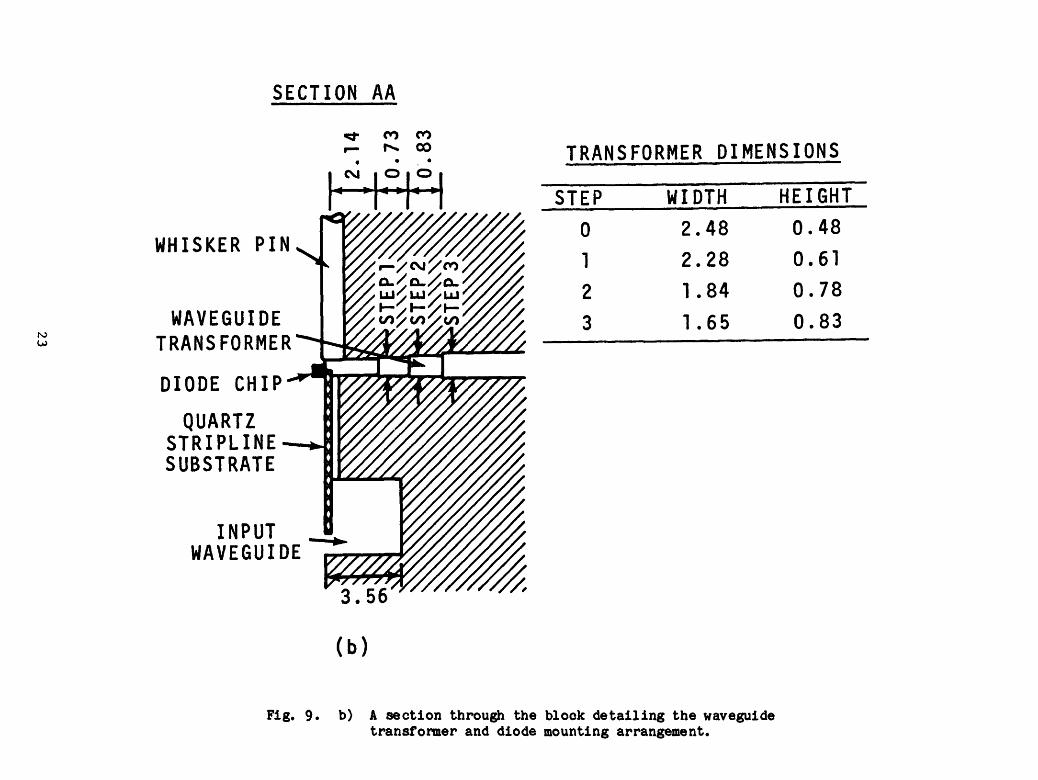
Fig. 9* b) A section through the block detailing the waveguide transformer and diode mounting arrangement.
bias line approximates a quarter-wave, short circuited stub at 50 GHz, thus
minimizing the effect of the bias circuit on the performance of the lowpass
filter near cut-off.
A quarter-wave, two section impedance transformer couples the 2.48 mm x
0.48 mm reduced height guide to the 1.66 mm x 0.83 mm output guide. Power can
flow in the wider guide at the second harmonic, whereas the output guide is
cut off at this frequency. The transformer is thus used to implement a reactive
second harmonic idler termination by spacing it approximately X /2 (at the second
harmonic wavelength) from the plane of the diode.
The varactor diode is a Schottky-barrier device fabricated by R. Mattauch
at the University of Virginia (designated 8P2) with a zero bias capacitance
of 28 fF, a DC series resistance of 10.3 ohms and a breakdown voltage of 20
volts at 1 uA. These devices have a highly non-linear capacitance versus voltage
law which approximates the inverse half power behaviour of an ideal abrupt junction
varactor to within 5 volts of the breakdown limit.
The performance of the multiplier has been measured at 1500 MHz intervals
for output frequencies between 90 and 120 GHz. The output power response as
a function of output frequency for constant 50 mW pump power is shown in Figure
10. Backshort tuning and DC bias were optimized at each measurement frequency.
Typically the bias conditions for optimum performance were a reverse bias voltage
of about 4 volts and a forward current between 1 mA and 4 mA. More than 2 mW
output power is obtained at any frequency between 90 and 120 GHz, corresponding
to a minimum conversion efficiency, for 50 mW pump power of 4$. The peak output
power obtained was 4 mW at 110 GHz, corresponding to an efficiency of 8%.
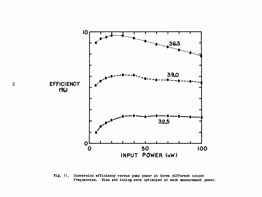
Figure 11 shows how the multiplier conversion efficiency varies with pump
power at three different output frequencies. Bias and tuning were optimized
24
10
OUTPUT POWER
(MW)
/
S-K^^ \:
\
/
X—x—
B <r'X .„■'•- ••••••...A.***1 >•• • . ••!
X-^A
•••
0 90
i
105 OUTPUT FRECXUENCY (GHz)
120
Fig. 10. Output power versus output frequency for the tripler: A) at constant 50 mW input power (from a klystron source) and B) when pumped ty the 26.5-40 GHz YIG oscillator. For curve A), the tripler bias and tuning were optimized at each frequency, whereas for curve B) the tuning was optimized but the bias was fixed, as described in the text,
10
to EFFICIENCY (%)
- f'
1 ■ ' "••• A
—i 1 1—
-• .36£ •
—i
-• -
:. - • *
•"•-•.. 39.0 _
w w — — 9 -. —•—i
-
^—•—•- — t • #— —t—i
./^
32.5
50 INPUT POWER (MW)
100
Fig. 11. Conversion efficiency versus pump power at three different output frequencies. Bias and tuning were optimized at each measurement power.
for best performance at each pump level. Although the tripler can safely handle
input powers of up to 120 mW, the best conversion efficiency occurs at input
powers of about 30 mW.
IV. The Complete Synthesized LO Source
Figure 10 shows the output power response of the complete synthesized LO
system, with the tripler pumped by the phase locked, YIG-tuned Gunn oscillator.
More than 1 mW output power is available at any frequency between 90 and 120 GHz
when the tripler tuning is optimized at each operating frequency. The tripler
bias was fixed at a voltage of 3.5 volts for these measurements. The tuning
curves (position vs. operating frequency) for the tripler backshorts are monotonic
and very repeatable. Motorized servo tuning of the multiplier backshorts could
easily be implemented automatically by using the frequency select input, resulting
in completely automatic operation of the synthesized local oscillator system.
V. Summary
The synthesized 90-120 GHz local oscillator system described in this paper
was designed for use with cooled Schottky diode or SIS mixer heterodyne radiometers.
The system is fully automatic in operation and exhibits adequate output power,
wide tuning range and excellent frequency stability, making it an ideal choice
for application as an L0 source in millimeter-wave spectrometer receivers.
There clearly exist other areas of application for such a signal source. Some
possibilities are: i) as a phase stable local oscillator for the receivers
in a phase coherent millimeter wave antenna array, ii) as a synthesized swept
frequency signal generator for laboratory test applications. The unit described
here is to be incorporated in the near future into a 100-120 GHz SIS receiver
27
system [12] to be installed on the NRAO 12 meter diameter radio telescope near
Tucson, Arizona.
VI. Acknowledgments
The authors gratefully acknowledge the assistance of N. Horner Jr. who
assembled the tripler block and G. Taylor who fabricated the tripler mount.
Prof. R. Mattauch of the University of Virginia is thanked for providing the
Schottky diodes used in the multiplier. Thanks also go to M. Balister who provided
helpful comments and advice during the construction of the synthesizer.
28
References
1. J. W. Archer, "All Solid-State Receiver for 210-240 ftHgr* TREE frana ^n
HIL., vol. MTT-30, p. 1247, August 1982.
2. N. R. Erickson, BA High Efficiency Frequency Tripler for 230 GHz," Proo.
12th Evr. Micr. Conf. > (Helsinki, Finland), p. 288, Sept 1982.
3. J. E. Carlstrom, R. L. PI am beck and D. D. Thornton, "A 60-115 GHz Tuneable
Gunn 0301113^^, submitted for publication to IEEE Trans, on MTT.
August 1984.
4. C. R. Predmore, N. R. Erickson, P. F. Goldsmith and J. L. R. Marrero, "A
Broadband Ultra Low-Noise Schottky Diode Mixer Receiver from 80 to
115 GHz," IEEE Trans, on MTT. vol. MrT-32, p. 498, May 1984.
5. J. W. Archer and M. T. Faber, "A Very Low-Noise Receiver for 80 to 120
GHz." Int. J. I. R. and MM-Wavesr vol. 5, no 8, p. 1069, August 1984.
6. S-K. Pan, M. J. Feldman, A. R. Kerr and P. Timbie, "A Low Noise 115 GHz
Receiver Using Superconducting Tunnel Junctions," ADD. Phys. Lett..
vol. 43, P. 786, 1983.
7. L. R. D^ddario, "A 90-120 GHz SIS Mixer Having Gain and Wide Bandwidth,"
Int. J. I.R. and MM-Wavesr vol. 5, no. 10, October 1984.
8. F. M. Gardner, "Phaselock Techniques", p. 208, John Wiley, New York, 1979.
9. "Pulse Swallowing Revisited," Fairchild ECL Data Book, p. 9-56/581, Fairchild
Camera and Instrument Corp., Mountain View, CA, 1977.
10. F. M. Gardner, ibidf p. 11.
11. J. W. Archer, "An Efficient 200-290 GHz Frequency Tripler Incorporating
a Novel Stripline Structure," TEfif. Trans, on MTT. vol. MTT-32,
p. 416, April 1984.
29
12. J.W. Archer, "A High Performance, 2.5K Cryostat Incorporating a 100-120
GHz Dual Polarization Receiver", submitted for publication to Rev.
Soi. Instr.. October 1984.
30