Electronic Supporting Information (ESI) Supporting Information (ESI) ... while emission spectra were...
11
S1 Electronic Supporting Information (ESI) Perylenetetracarboxylic-metal assemblies and anisotropic charge transport in the Cu II assembly Linyi Bai, a Youyi Xia, a Avijit Jana, a Chung Yen Ang, a Lingzhi Zhao, a Zhi Fan,* ,b and Yanli Zhao* ,a,c [a] Division of Chemistry and Biological Chemistry, School of Physical and Mathematical Sciences, Nanyang Technological University, 21 Nanyang Link, Singapore 637371 [b] College of Chemical Engineering and Materials Science, Tianjin University of Science and Technology, Tianjin 300457, China [c] School of Materials Science and Engineering, Nanyang Technological University, 50 Nanyang Avenue, Singapore 639798 *To whom correspondence should be addressed Email: [email protected]; [email protected] Electronic Supplementary Material (ESI) for Nanoscale. This journal is © The Royal Society of Chemistry 2016
Transcript of Electronic Supporting Information (ESI) Supporting Information (ESI) ... while emission spectra were...

S1
Electronic Supporting Information (ESI)
Perylenetetracarboxylic-metal assemblies and anisotropic charge transport in the CuII assembly
Linyi Bai,a Youyi Xia,a Avijit Jana,a Chung Yen Ang,a Lingzhi Zhao,a Zhi Fan,*,b and Yanli Zhao*,a,c
[a] Division of Chemistry and Biological Chemistry, School of Physical and Mathematical Sciences, Nanyang Technological University, 21 Nanyang Link, Singapore 637371
[b] College of Chemical Engineering and Materials Science, Tianjin University of Science and Technology, Tianjin 300457, China
[c] School of Materials Science and Engineering, Nanyang Technological University,50 Nanyang Avenue, Singapore 639798
*To whom correspondence should be addressed
Email: [email protected]; [email protected]
Electronic Supplementary Material (ESI) for Nanoscale.This journal is © The Royal Society of Chemistry 2016

S2
1. Instruments
1.1 Thermogravimetric analysis (TGA) & Fourier transform infrared (FT-IR) experimentsTGA was performed on a TGA 500 thermogravimetric analyzer by heating the samples at 20 C min-1 to 1000 C in a nitrogen atmosphere (60 mL/min). FTIR spectra (KBr, Aldrich) were measured with an SHIMADZU IR Prestige-21 spectrometer. Samples were packed firmly to obtain transparent films.
1.2 Powder XRD measurements and scanning electron microscopy (SEM)Powder XRD studies were performed on a SHIMADZU XRD-6000 Labx diffractometer, using Cu-Ka radiation (40 kV, 300 mA) with a scanning rate of 0.02o s-1 (2θ) at room temperature. SEM images were collected on a field emission JSM-6700F (JEOL) operated at 10 kV.
1.3 ICP-MSThe contents of metal ions and sodium ions in the samples were estimated by using a Perkin-Elmer Optima 2100 DV Inductive Coupled Plasma Mass Spectroscopy (ICP-MS). Then, the concentrations of metal ions were recorded and summarized in Table S1.
1.4 UV-vis absorption, fluorescence & CD spectraAbsorption spectra were recorded on UV-3600 UV−vis−NIR spectrophotometer (Shimadzu), while emission spectra were recorded on RF-5301 PC spectrofluorophotometer (Shimadzu) with 1.0 cm path length cell. CD spectra were recorded on a Jasco J-810 CD spectrophotometer.
1.5 X-ray photoelectron spectroscopy (XPS) measurementsXPS measurements were performed with a Phiobos 100 spectrometer using Mg X-ray radiation source (SPECS, Germany) for wide range and high resolution scans at 12.53 kV. The XPS samples were coated on a conductive carbon tape that was then fixed on am aluminum XPS holder.
2. Sample preparation
Materials synthesis: solvents and all other chemicals were obtained from commercial sources and were used without further purifications. Firstly, PTCDA powder (0.39 g, 1 mM) was dispersed in a mixed solvent of THF and MeOH (VTHF : VMeOH = 1:1, 100 mL). NaOH with 4 times of mole ratio of PTCDA was dissolved in an equal volume of water, which was added slowly into the stirring PTCDA solution in a dropwise fashion. The resulted solution was brought to reflux for 2 h in order to ensure a complete deprotonation to afford Na4PTC.
For the preparation of metal complexes, two typical methods were employed, where one involved the rapid mixing of individual components (i.e., metal ions and Na4PTC), while the other was the slow diffusion of two separated components. In the rapid mixing synthesis process, a stock solution of Na4PTC (C = 10 mM, 4 mL) was mixed rapidly with an equal volume of metal salt solution (C = 10 mM) in THF/MeOH under vigorous stirring. After several hours, solid precipitates appeared in the resultant solution were obtained by centrifuging for 3 times in water at 5000 rpm for 5 min each. Other metal-PTC complexes were synthesized following a similar experimental procedure using different concentrations of metal ions. In the slow diffusion synthesis process, the solution of Na4PTC was prepared firstly, and then the solution of metal salt with a proper molar ratio (1:1 for Ag+, 2:1 for Zn2+, 2:1 for Cu2+ and 4:1 for Zr4+) was dropped slowly to the Na4PTC solution to form the precipitates over 12 h without stirring.
For the samples used in XPS and ICP-MS tests, they were centrifuged 3 times in water at 5000 rpm for 5 min to ensure that the sodium salt was totally removed.

S3
Fig. S1. Morphologies of complexes obtained by the rapid mixing method using Na4PTC with various metal salts: (a-c) Ag+ salts, (d-f) Cu2+ salts, (g-i) Zn2+ salts, and (j-l) Zr4+ salts.
3. Physical properties of complexes
011
021
042
102
110
(a) (b)
250 300 350 400 450 500 550 600 650 700 750Ads
orpt
ion
Inte
nsity
/ a.
u.
Wavelength / nm
Na4PTC
5 10 15 20 25 30 35 402θ / o
Rel
ativ
e In
tens
ity (a
.u.) Na4PTC
Fig. S2. (a) UV absorption spectra and (b) powder X-ray diffraction pattern of Na4PTC.

S4
Fig. S3. UV absorption spectra of Na4PTC with various metal salts having (a) acetate, (b) nitrate, and (c) chloride counter anions.
1200 1000 800 600 400 200 0
Na-2s
Ag+/Na4PTC
Cu2+/Na4PTC
Zn2+/Na4PTC
Zr4+/Na4PTC
Na-2s
Zn-3s
Ag-4sO-1s
Rel
ativ
e In
tens
ity (a
.u.)
Binding Energy (eV)
C-1s
Zr-3d
Cu-3s
Na-KLLNa-2s
Fig. S4. XPS spectra of various complexes Mn+/Na4PTC.

S5
Table S1. Composition of metal ions / Na4PTC complex assemblies determined by ICP-MS.
Sample Theoretical ratio of metal ions to Na+
concentrationPractical ratio of metal ions to Na+
concentrationAg+/Na4PTC 1:2 0.52Cu2+/Na4PTC 1:4 0.27Zn2+/Na4PTC 1:4 0.28Zr4+/Na4PTC 1:8 No Na+
Fig. S5. Proposed mechanism for the formation of the complex assemblies: (a) Ag+/Na4PTC; (b) Cu2+/Na4PTC; (c) Zn2+/Na4PTC; (d) Zr4+/Na4PTC.
S6
Fig. S6. (a) Schematic representation of the twisting nanorods; (b) CD spectra indicating the signals of chirality changes during the growth of twisting nanorods; (c-e) twisting nanorods with different pitches for various anion salts.
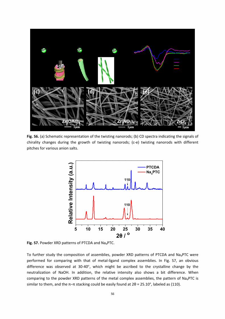
5 10 15 20 25 30 35 40
110
PTCDA Na4PTC
2θ / o
Rel
ativ
e In
tens
ity (a
.u.)
110
Fig. S7. Powder XRD patterns of PTCDA and Na4PTC.
To further study the composition of assemblies, powder XRD patterns of PTCDA and Na4PTC were performed for comparing with that of metal-ligand complex assemblies. In Fig. S7, an obvious difference was observed at 30-40, which might be ascribed to the crystalline change by the neutralization of NaOH. In addition, the relative intensity also shows a bit difference. When comparing to the powder XRD patterns of the metal complex assemblies, the pattern of Na4PTC is similar to them, and the π–π stacking could be easily found at 2θ = 25.10°, labeled as (110).

S7
It is well known that the electron transport is qualitatively consistent with molecular packing structures. The growth of metal-PTC complex assemblies is the competition outcome between π–π stacking interaction and metal-ligand coordination. Thus, it was hypothesized the microstructures growing at different dimension offer an anisotropic electron transport, which could be verified through the OFET performance.
4. Theoretical calculations for HOMO and LUMO orbital
Table S2. Theoretical HOMO and LUMO orbital of metal/Na4PTC complexes.
HOMO LUMO Orbital No.PTCDA 110-111
Ag+/Na4PTC 119-120
Cu2+/Na4PTC 119-120
Zn2+/Na4PTC 115-116
Zr4+/Na4PTC 115-116
5. Field-effect transistor (FET) device fabrication
(1) Device fabrication:Heavily p-doped Si substrates with thermally grown SiO2 (300 nm) layer were cleaned by two
rounds of sonication in acetone and iso-propyl alcohol (20 minutes each round, and then dried under nitrogen flow). By using another photolithographic process, high-density patterned metallic electrodes (10 nm of Cr followed by 80 nm of Au) were introduced and separated by 7 µm in the center. With the metal pads as source (S) and drain (D) contacts and the silicon substrate as a back gate (G), the devices can be electrically tested. Before dropping the active materials, an oxygen plasma cleaning treatment was performed on the substrate for 1 minute to improve the wetting of the surface.(2) Deposition:
The metal/Na4PTC hybrid materials were dispersed in a mixing solvent of THF/methanol (v:v =

S8
3:7). In order to obtain dispersed solution, slight shaking or sonicating was performed. Then, the solution was dropped on the substrate prepared before. The resulted substrate was finally annealed at 100 °C for 30 minutes for solvent removal. The device characterization was carefully carried out at room temperature in the ambient atmosphere using an Agilent 4155C semiconductor characterization system (DC measurements) and a Karl Suss (PM5) manual probe station.
Fig. S8. Photos of crystal devices corresponding to the assemblies of (a) Cu2+/Na4PTC and (b) Zn2+/Na4PTC. Only Cu2+/Na4PTC-based device was qualified for anisotropic electron transport measurements on account of its suitable crystal size.
-20 -10 0 10 20
10-6
10-5
10-4
On/off ratio=~103
μ=0.03 cmV-1S-1
Vg(V)
I d(A)
-1.0x10⁻⁷
-5.0x10⁻⁸
0.0
I G(A)
-10 0 10 20 30
10-7
10-6 I g(A
)
Vg(V)
I d(A
)
-2x10⁻¹⁰
-1x10⁻¹⁰
0
(a) (b)
Fig. S9. (a) Transfer and (b) output characteristics of a Cu2+/Na4-PTC single-plate transistor along a and b axes, respectively.
6. Reproducibility
Based on the performance of all the devices, we summarized the reproducibility under each condition. Firstly, the average value of charge mobility was calculated based on 3 devices under each condition. Then, the standard deviation of mobility could be obtained to show the distribution range of mobility under each condition.

S9
-10 0 10 20 30 40 50
0.000
0.005
0.010
0.015
0.020
0.025
0.030
Cha
rge
mob
ility
(cm
2 V-1S-1
)
Gate voltage (V)
a axis b axis
Fig. S10. Statistic standard deviation of charge mobility along a and b axes for the reproducibility of field-effect transistors.
7. Appendix

S10

S11