
Electronic Circuit Casebook - RIT - People · PDF file1 1 INDETERMINATE B C R 0 0 ......
63
© May 10, 2009 Dr. Lynn Fuller Electronic Circuit Casebook Page 1 Rochester Institute of Technology Microelectronic Engineering ROCHESTER INSTITUTE OF TECHNOLOGY MICROELECTRONIC ENGINEERING Electronic Circuit Casebook Dr. Lynn Fuller Webpage: http://people.rit.edu/lffeee Microelectronic Engineering Rochester Institute of Technology 82 Lomb Memorial Drive Rochester, NY 14623-5604 Tel (585) 475-2035 Fax (585) 475-5041 Email: [email protected] Department webpage: http://www.microe.rit.edu 5-10-2009 Electronic_Circuit_Casebook.ppt
Transcript of Electronic Circuit Casebook - RIT - People · PDF file1 1 INDETERMINATE B C R 0 0 ......

© May 10, 2009 Dr. Lynn Fuller
Electronic Circuit Casebook
Page 1
Rochester Institute of TechnologyMicroelectronic Engineering
ROCHESTER INSTITUTE OF TECHNOLOGYMICROELECTRONIC ENGINEERING
Electronic Circuit Casebook
Dr. Lynn Fuller Webpage: http://people.rit.edu/lffeee Microelectronic Engineering
Rochester Institute of Technology 82 Lomb Memorial Drive Rochester, NY 14623-5604 Tel (585) 475-2035 Fax (585) 475-5041
Email: [email protected] Department webpage: http://www.microe.rit.edu
5-10-2009 Electronic_Circuit_Casebook.ppt

© May 10, 2009 Dr. Lynn Fuller
Electronic Circuit Casebook
Page 2
Rochester Institute of TechnologyMicroelectronic Engineering
OUTLINE
Power Conditioning, Voltage RegulatorsAnalog Switches, Two Phase ClocksVoltage Inverters, DoublersAmplifiers, Log AmplifiersRC OscillatorsVoltage Controlled Oscillators

© May 10, 2009 Dr. Lynn Fuller
Electronic Circuit Casebook
Page 3
Rochester Institute of TechnologyMicroelectronic Engineering
INTRODUCTION
This document contains information on some electronic circuits that have been used as subcomponents in various microsystems. In general these circuits are realized using a hybrid combination of packaged integrated circuits, passive and active components combined at the printed circuit board (PCB) level. Some circuitshave been converted to custom CMOS integrated circuits to provide on chip electronics and signal conditioning for MEMS devices.
© May 10, 2009 Dr. Lynn Fuller
Electronic Circuit Casebook
Page 4
Rochester Institute of TechnologyMicroelectronic Engineering
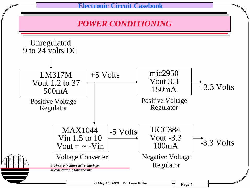
POWER CONDITIONING
Unregulated9 to 24 volts DC
MAX1044Vin 1.5 to 10Vout = ~ -Vin
LM317MVout 1.2 to 37
500mA
UCC384Vout -3.3100mA
Negative Voltage Regulator
Positive Voltage Regulator
Voltage Converter
mic2950Vout 3.3150mA
+5 Volts+3.3 Volts
-5 Volts-3.3 Volts
Positive Voltage Regulator

© May 10, 2009 Dr. Lynn Fuller
Electronic Circuit Casebook
Page 5
Rochester Institute of TechnologyMicroelectronic Engineering
BASIC VOLTAGE REGULATOR
Vout
R1
R2Gnd
UnregulatedPower Supply
(e.g. transformer,
rectifier, capacitor filter)
BJT or MOS Transistor Pass
Element
Vref
RLoad-+Av
+-
Voltage Regulator
Vout = Vref(1+R2/R1)
-+ Vx

© May 10, 2009 Dr. Lynn Fuller
Electronic Circuit Casebook
Page 6
Rochester Institute of TechnologyMicroelectronic Engineering
VOLTAGE REGULATOR
LM317MVout 1.2 to 37
500mA
Positive Voltage Regulator
Vout = 1.25(1+R2/R1)
Vin VoutR1
R2Gnd
See: data sheets for LM317M-D.pdf
© May 10, 2009 Dr. Lynn Fuller
Electronic Circuit Casebook
Page 7
Rochester Institute of TechnologyMicroelectronic Engineering
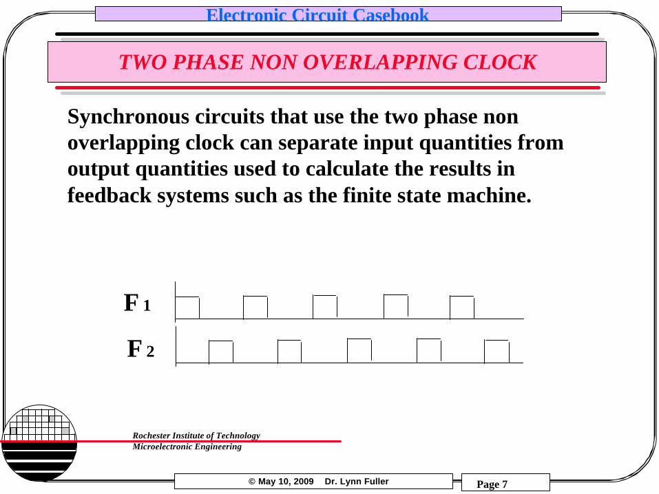
TWO PHASE NON OVERLAPPING CLOCK
Synchronous circuits that use the two phase non overlapping clock can separate input quantities from output quantities used to calculate the results in feedback systems such as the finite state machine.
Φ1
Φ2

© May 10, 2009 Dr. Lynn Fuller
Electronic Circuit Casebook
Page 8
Rochester Institute of TechnologyMicroelectronic Engineering
TWO-PHASE CLOCK GENERATORS
CLOCKBAR
Φ1
Φ2
CLOCK Φ1
Φ2
CLOCKBAR
CLOCK
t1
t3
t2
t1
t3
t1
QS
0 0 Qn-10 1 11 0 01 1 INDETERMINATE
RCB
0 0 10 1 01 0 01 1 0
A
S
RQ
t2
=
© May 10, 2009 Dr. Lynn Fuller
Electronic Circuit Casebook
Page 9
Rochester Institute of TechnologyMicroelectronic Engineering
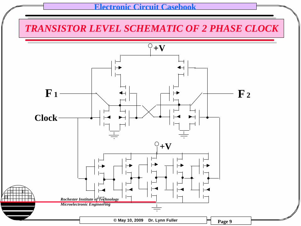
TRANSISTOR LEVEL SCHEMATIC OF 2 PHASE CLOCK
+V
Φ1 Φ2
+V
Clock

© May 10, 2009 Dr. Lynn Fuller
Electronic Circuit Casebook
Page 10
Rochester Institute of TechnologyMicroelectronic Engineering
LAYOUT OF TWO PHASE CLOCK
CLOCKBAR
CLOCK Φ1
Φ2t3
t2
t1
S
RQ

M3 M5
M4 M6
3 4
M1
M2
2V15V
+-
1
TwoPhaseClock1.txt
0
V2CLOCK
+-
8
765
9
Substrate of all NMOS go to ground, node 0Substrate of all PMOS go to +5V, node 1
M9
M10
M7
M8
M11
M12
M13
M14
M15
M16
M17
M18
VOUT1 VOUT210 11

© May 10, 2009 Dr. Lynn Fuller
Electronic Circuit Casebook
Page 12
Rochester Institute of TechnologyMicroelectronic Engineering
WINSPICE SIMULATION

© May 10, 2009 Dr. Lynn Fuller
Electronic Circuit Casebook
Page 13
Rochester Institute of TechnologyMicroelectronic Engineering
TWO PHASE NON OVERLAPPING CLOCK
Clock
Φ1
Φ2

© May 10, 2009 Dr. Lynn Fuller
Electronic Circuit Casebook
Page 14
Rochester Institute of TechnologyMicroelectronic Engineering
VERSION 2 OF TWO PHASE NON OVERLAPPING CLOCK
CLOCKBAR
CLOCK Φ1
Φ2t3
t2
t1
S
R
2
V15V
+-
1
0
V2CLOCK
+-
M5
M7
M6 M16
3 4
M3
M4
8
76
9
M1
M2
5
M9
M10
M11
M12
M13
M14
M15
M18
M17
M8
VOUT1 VOUT210 11

© May 10, 2009 Dr. Lynn Fuller
Electronic Circuit Casebook
Page 15
Rochester Institute of TechnologyMicroelectronic Engineering
WINSPICE SIMULATION
© May 10, 2009 Dr. Lynn Fuller
Electronic Circuit Casebook
Page 16
Rochester Institute of TechnologyMicroelectronic Engineering
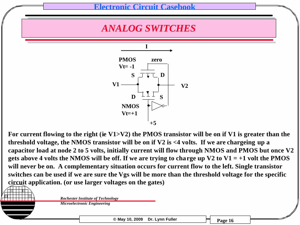
ANALOG SWITCHES
For current flowing to the right (ie V1>V2) the PMOS transistor will be on if V1 is greater than thethreshold voltage, the NMOS transistor will be on if V2 is <4 volts. If we are chargeing up a capacitor load at node 2 to 5 volts, initially current will flow through NMOS and PMOS but once V2 gets above 4 volts the NMOS will be off. If we are trying to charge up V2 to V1 = +1 volt the PMOS will never be on. A complementary situation occurs for current flow to the left. Single transistor switches can be used if we are sure the Vgs will be more than the threshold voltage for the specific circuit application. (or use larger voltages on the gates)
NMOSVt=+1
PMOSVt= -1
DS
I
zero
V1 V2
+5
SD

© May 10, 2009 Dr. Lynn Fuller
Electronic Circuit Casebook
Page 17
Rochester Institute of TechnologyMicroelectronic Engineering
(+V to -V) ANALOG SWITCH WITH (0 to 5 V) CONTROL
DS
0-5V Logic Control
Vout
+5
SDVin
+V
-V

© May 10, 2009 Dr. Lynn Fuller
Electronic Circuit Casebook
Page 18
Rochester Institute of TechnologyMicroelectronic Engineering
SWITCHED CAPACITOR VOLTAGE DOUBLER
VddC1
Φ1
Φ2
C1
Φ2
Φ1
Φ1Φ1
Φ2
CLoad RLoad

© May 10, 2009 Dr. Lynn Fuller
Electronic Circuit Casebook
Page 19
Rochester Institute of TechnologyMicroelectronic Engineering
BASIC TWO STAGE OPERATIONAL AMPLIFIER
© May 10, 2009 Dr. Lynn Fuller
Electronic Circuit Casebook
Page 20
Rochester Institute of TechnologyMicroelectronic Engineering
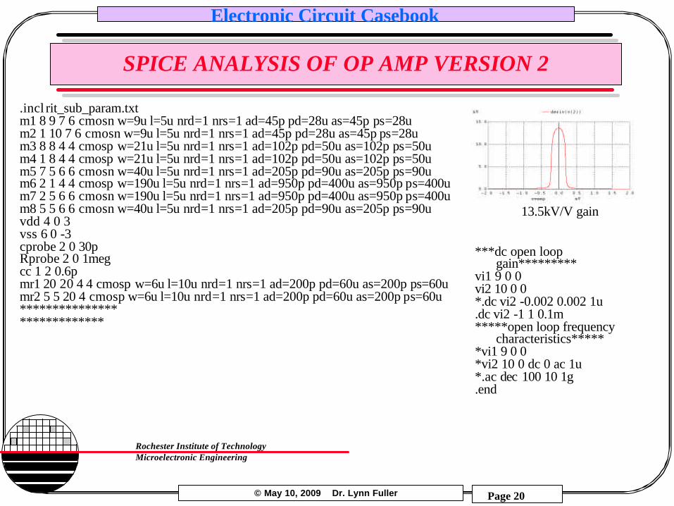
SPICE ANALYSIS OF OP AMP VERSION 2
.incl rit_sub_param.txtm1 8 9 7 6 cmosn w=9u l=5u nrd=1 nrs=1 ad=45p pd=28u as=45p ps=28um2 1 10 7 6 cmosn w=9u l=5u nrd=1 nrs=1 ad=45p pd=28u as=45p ps=28um3 8 8 4 4 cmosp w=21u l=5u nrd=1 nrs=1 ad=102p pd=50u as=102p ps=50um4 1 8 4 4 cmosp w=21u l=5u nrd=1 nrs=1 ad=102p pd=50u as=102p ps=50um5 7 5 6 6 cmosn w=40u l=5u nrd=1 nrs=1 ad=205p pd=90u as=205p ps=90um6 2 1 4 4 cmosp w=190u l=5u nrd=1 nrs=1 ad=950p pd=400u as=950p ps=400u m7 2 5 6 6 cmosn w=190u l=5u nrd=1 nrs=1 ad=950p pd=400u as=950p ps=400u m8 5 5 6 6 cmosn w=40u l=5u nrd=1 nrs=1 ad=205p pd=90u as=205p ps=90uvdd 4 0 3vss 6 0 -3cprobe 2 0 30pRprobe 2 0 1megcc 1 2 0.6pmr1 20 20 4 4 cmosp w=6u l=10u nrd=1 nrs=1 ad=200p pd=60u as=200p ps=60umr2 5 5 20 4 cmosp w=6u l=10u nrd=1 nrs=1 ad=200p pd=60u as=200p ps=60u****************************
***dc open loop gain*********
vi1 9 0 0vi2 10 0 0 *.dc vi2 -0.002 0.002 1u.dc vi2 -1 1 0.1m*****open loop frequency
characteristics******vi1 9 0 0 *vi2 10 0 dc 0 ac 1u*.ac dec 100 10 1g.end
13.5kV/V gain

© May 10, 2009 Dr. Lynn Fuller
Electronic Circuit Casebook
Page 21
Rochester Institute of TechnologyMicroelectronic Engineering
OPERATIONAL AMPLIFIER

© May 10, 2009 Dr. Lynn Fuller
Electronic Circuit Casebook
Page 22
Rochester Institute of TechnologyMicroelectronic Engineering
SOME BASIC ANALOG ELECTRONIC CIRCUITS
These circuits should be familiar:
-
+VoVin
R2R1
Inverting Amplifier
-
+Vo
Vin
R2R1
Non-Inverting Amplifier
-
+
Unity Gain Buffer
-
+VoVin
C
R
Integrator
VinVo
Vo= - Vin R2/R1
Vo= Vin
Vo= Vin (1 + R2/R1)
Vo= -1/RC Vin dt

© May 10, 2009 Dr. Lynn Fuller
Electronic Circuit Casebook
Page 23
Rochester Institute of TechnologyMicroelectronic Engineering
COMPARATOR
-+
VoVin
Vo
Vin
Vref
+V
-VVref
+V
-V
+V-V
Measured
Theoretical

© May 10, 2009 Dr. Lynn Fuller
Electronic Circuit Casebook
Page 24
Rochester Institute of TechnologyMicroelectronic Engineering
BISTABLE CIRCUIT WITH HYSTERESIS
-+ Vo
Vin
+V
-V
R2R1 Vo
VinVTH
+V
-V
VTL
Sedra and Smith pg 1187Measured
Theoretical

© May 10, 2009 Dr. Lynn Fuller
Electronic Circuit Casebook
Page 25
Rochester Institute of TechnologyMicroelectronic Engineering
RC INTEGRATOR
C
VoutR
Vin
Vin
t+Va
-Va
Vout
t+Va
-Va
Smaller RC
t1
Vout = (-Va) + [2Va(1-e-t/RC)] for 0<t<t1
If R=1MEG and C=10pF find RC=10us so t1 might be ~20us

© May 10, 2009 Dr. Lynn Fuller
Electronic Circuit Casebook
Page 26
Rochester Institute of TechnologyMicroelectronic Engineering
OSCILLATOR (MULTIVIBRATOR)
-+ Vo
C
+V
-V
R2R1
R
Vo
tt1
VT
+V
-V
Bistable Circuit with Hysteresis and RC Integrator

© May 10, 2009 Dr. Lynn Fuller
Electronic Circuit Casebook
Page 27
Rochester Institute of TechnologyMicroelectronic Engineering
RIT 100X DIFFERENTIAL VOLTAGE AMPLIFIER
1” X 1.5”
Vo1-+
RinRf
Vb-+
Va
-+Rf
Gnd
Rin
Vo2-+
RinRf
Gnd
Va
VbRf = 100KRin = 10K
© May 10, 2009 Dr. Lynn Fuller
Electronic Circuit Casebook
Page 28
Rochester Institute of TechnologyMicroelectronic Engineering
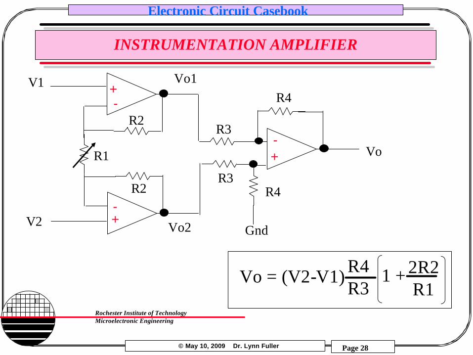
INSTRUMENTATION AMPLIFIER
Vo-+
R3
R4
Vo2+-
Vo1
-+
R4
Gnd
R3
V1
V2
R2
R1
R2
Vo = (V2-V1) R4R3
2R2R1
1 +

© May 10, 2009 Dr. Lynn Fuller
Electronic Circuit Casebook
Page 29
Rochester Institute of TechnologyMicroelectronic Engineering
CIRCUIT FOR LOW FREQUENCY CV MEASUREMENTS
Vout = (C R1 R3 / R2) (dVin/dt)
R1=18 Mohm
R2=1 Kohm
R3=33 Kohm
Vout
-
++
-
C
+
Vin
LM081 LM081-
1 V/secRamp

© May 10, 2009 Dr. Lynn Fuller
Electronic Circuit Casebook
Page 30
Rochester Institute of TechnologyMicroelectronic Engineering
C-V MEASUREMENTS ON N-TYPE SILICON
V0
C
High Frequency
Low Frequency
Accumulation
Depletion
Inversion
VFBVT
Cmin
CFB

© May 10, 2009 Dr. Lynn Fuller
Electronic Circuit Casebook
Page 31
Rochester Institute of TechnologyMicroelectronic Engineering
C-V MEASUREMENTS ON P-TYPE SILICON
V0
C
High Frequency
Low Frequency
Accumulation
Depletion
Inversion
VFB VT
Cmin
CFB

© May 10, 2009 Dr. Lynn Fuller
Electronic Circuit Casebook
Page 32
Rochester Institute of TechnologyMicroelectronic Engineering
PEAK DETECTOR
-
+Vo
C
Variable Vin
Diode reverse leakage current ~100nA

© May 10, 2009 Dr. Lynn Fuller
Electronic Circuit Casebook
Page 33
Rochester Institute of TechnologyMicroelectronic Engineering
DESIGN EXAMPLE – CAPACITOR SENSOR
-+
C
+V
-V
R2R1
R
C
+-
Vo
Vref -VC
R
-
+
Square WaveGenerator
ComparatorPeak Detector
RC Integrator
&Capacitor
Sensor
Buffer Display

© May 10, 2009 Dr. Lynn Fuller
Electronic Circuit Casebook
Page 34
Rochester Institute of TechnologyMicroelectronic Engineering
EXAMPLE LABORATORY RESULTS
Square WaveGenerator
OutputBufferOutput
Display
Smaller Capacitance
Larger Capacitance
© May 10, 2009 Dr. Lynn Fuller
Electronic Circuit Casebook
Page 35
Rochester Institute of TechnologyMicroelectronic Engineering
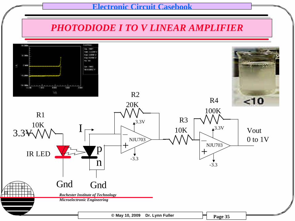
PHOTODIODE I TO V LINEAR AMPLIFIER
+pn
Vout0 to 1V
R2
I
Gnd
20K
3.3V
-3.3
3.3V
Gnd
IR LED +
R4100K
3.3V
-3.3
R310K
R110K
NJU703NJU703

© May 10, 2009 Dr. Lynn Fuller
Electronic Circuit Casebook
Page 36
Rochester Institute of TechnologyMicroelectronic Engineering
PHOTO DIODE I TO V LOG AMPLIFIER
+p
nVout0 to 1V
I
Gnd
3.3V
-3.3
NJU7033.3V
Gnd
IR LED
R120K
1N4448
Vout vs. Diode Current
0.0
0.5
1.0
1.5
2.0
2.5
3.0
3.5
0.01 0.1 1 10 100 1000 10000
Diode Current (uA)
Ou
tpu
t Vo
ltag
e (V
)
Linear AmplifierLog Amplifier
Linear amplifier uses 100K ohm in place of the 1N4448
Photodiode

© May 10, 2009 Dr. Lynn Fuller
Electronic Circuit Casebook
Page 37
Rochester Institute of TechnologyMicroelectronic Engineering
PHOTO DIODE I TO V INTEGRATING AMPLIFIER
Rf
-+
Ri-+
C
Reset
Internal100 pF
Analog Vout
Integrator and amplifier allow for measurement at low light levels
© May 10, 2009 Dr. Lynn Fuller
Electronic Circuit Casebook
Page 38
Rochester Institute of TechnologyMicroelectronic Engineering
SIGNAL CONDITIONING FOR TEMPERATURE SENSOR
p
n
Gnd
I3.3V
R120K
0.2 < Vout < 0.7V
+
-

© May 10, 2009 Dr. Lynn Fuller
Electronic Circuit Casebook
Page 39
Rochester Institute of TechnologyMicroelectronic Engineering
SIGNAL CONDITIONING FOR TEMPERATURE SENSOR
pMOSFET
Gnd
I
3.3V
0.2 < Vout < 0.7V
+
-
Constant Current Source

© May 10, 2009 Dr. Lynn Fuller
Electronic Circuit Casebook
Page 40
Rochester Institute of TechnologyMicroelectronic Engineering
OP AMP CONSTANT CURRENT SOURCE
Vo -+Vs
Vo+
RxR1L
oad
R
I = V
s/R
Floating Load Grounded Load
Vs
Loa
d
Rx/R1=R3/R2
I = Vs/R2
R3R2
© May 10, 2009 Dr. Lynn Fuller
Electronic Circuit Casebook
Page 41
Rochester Institute of TechnologyMicroelectronic Engineering
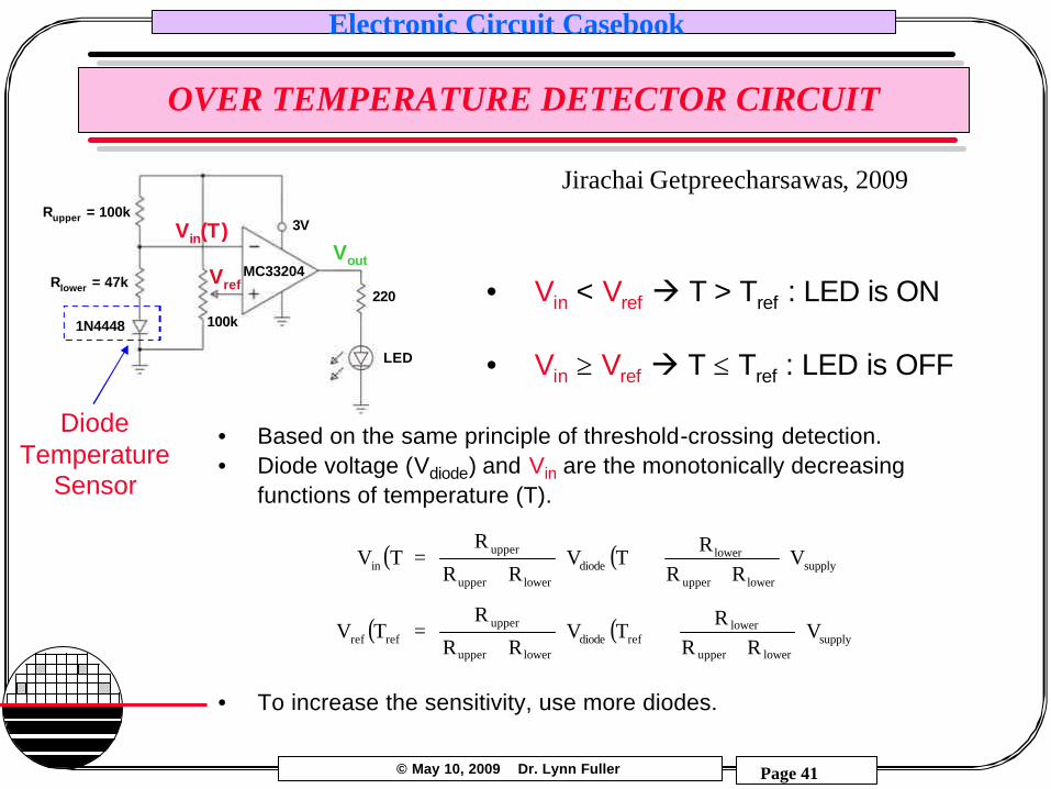
OVER TEMPERATURE DETECTOR CIRCUIT
• Based on the same principle of threshold-crossing detection.• Diode voltage (Vdiode) and Vin are the monotonically decreasing
functions of temperature (T).
• To increase the sensitivity, use more diodes.
Rlower = 47k
Rupper = 100k3V
100k
220
LED
MC33204
1N4448
DiodeTemperature
Sensor
• Vin < Vref à T > Tref : LED is ON
• Vin ≥ Vref à T ≤ Tref : LED is OFF
Vin(T)
Vref
Vout
( ) ( )
( ) ( ) supplylowerupper
lowerrefdiode
lowerupper
upperrefref
supplylowerupper
lowerdiode
lowerupper
upperin
VRR
RTV
RR
RTV
VRR
RTV
RR
RTV
++
+=
++
+=
Jirachai Getpreecharsawas, 2009

© May 10, 2009 Dr. Lynn Fuller
Electronic Circuit Casebook
Page 42
Rochester Institute of TechnologyMicroelectronic Engineering
WATER CONDUCTIVITY LOG I TO V AMPLIFIER
+Vout0 to 1V
Gnd
3.3V
-3.3
NJU703
1N4448
I
+Vg ~ - 0.1 V
Gnd
3.3V
-3.3
NJU703
320K
10K
-3.3
Conductivity (TDS)

© May 10, 2009 Dr. Lynn Fuller
Electronic Circuit Casebook
Page 43
Rochester Institute of TechnologyMicroelectronic Engineering
RC OSCILLATOR USING INVERTER WITH HYSTERESIS
1
2
V15V
+-
V2=0-5Or 5-0
+-
M12u/16u
R=10K
7
3Vout
M32u/15u
M22u/16u R
C
RC Oscillator
Inverter with Hysteresis
Vout

© May 10, 2009 Dr. Lynn Fuller
Electronic Circuit Casebook
Page 44
Rochester Institute of TechnologyMicroelectronic Engineering
RC OSCILLATOR, INVERTER WITH HYSTERESIS
3.0pF
1
2V19V
+-
M17
3
M3
M2
M4
C1
M5
M6
4M7 M8
All NMOS Realization
*TRANSISTORSM1 7 2 0 0 RITSUBN49 L=2U W=64U ad=96e-12 as=96e-12 pd=44e-6 ps=44e-6 nrd=0.025 nrs=0.025M2 3 2 7 0 RITSUBN49 L=2U W=16U ad=96e-12 as=96e-12 pd=44e-6 ps=44e-6 nrd=0.025 nrs=0.025M3 1 3 7 0 RITSUBN49 L=2U W=64U ad=96e-12 as=96e-12 pd=44e-6 ps=44e-6 nrd=0.025 nrs=0.025M4 1 1 3 0 RITSUBN49 L=32U W=8U ad=96e-12 as=96e-12 pd=44e-6 ps=44e-6 nrd=0.025 nrs=0.025M5 1 1 4 0 RITSUBN49 L=64U W=8U ad=96e-12 as=96e-12 pd=44e-6 ps=44e-6 nrd=0.025 nrs=0.025M6 4 3 0 0 RITSUBN49 L=2U W=128U ad=96e-12 as=96e-12 pd=44e-6 ps=44e-6 nrd=0.025 nrs=0.025M7 3 3 2 0 RITSUBN49 L=128U W=4U ad=96e-12 as=96e-12 pd=44e-6 ps=44e-6 nrd=0.025 nrs=0.025M8 3 2 2 0 RITSUBN49 L=64U W=4U ad=96e-12 as=96e-12 pd=44e-6 ps=44e-6 nrd=0.025 nrs=0.025*

© May 10, 2009 Dr. Lynn Fuller
Electronic Circuit Casebook
Page 45
Rochester Institute of TechnologyMicroelectronic Engineering
RC OSCILLATOR CMOS VERSION
© May 10, 2009 Dr. Lynn Fuller
Electronic Circuit Casebook
Page 46
Rochester Institute of TechnologyMicroelectronic Engineering
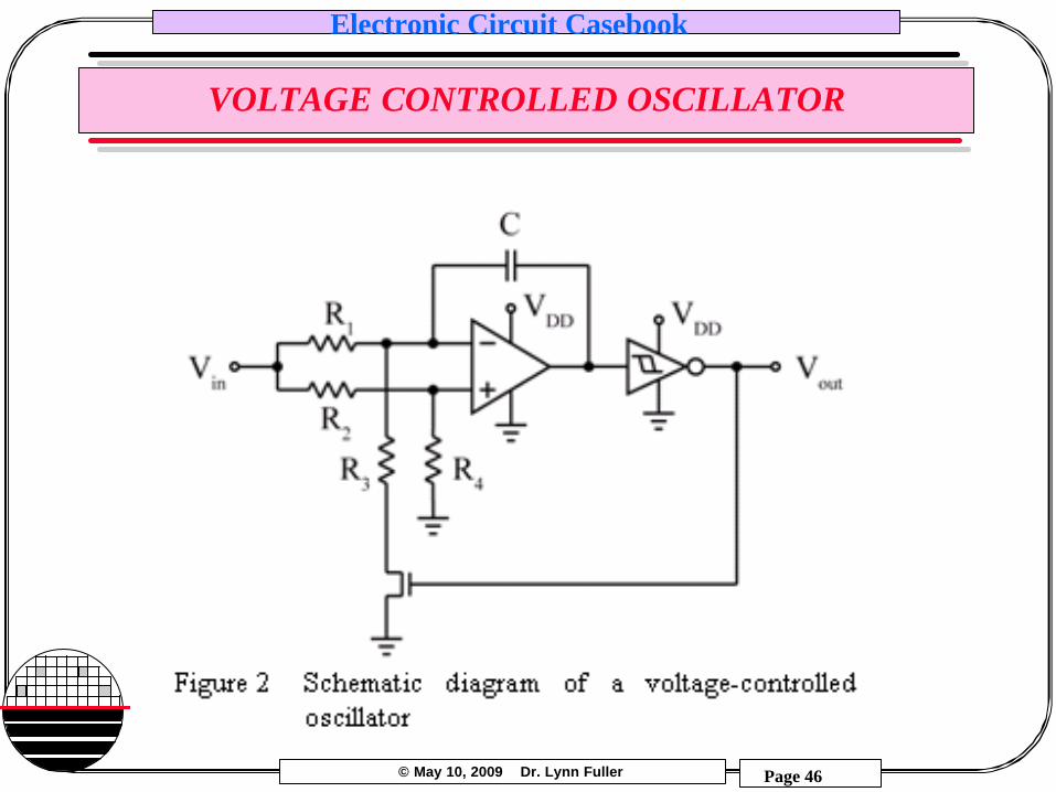
VOLTAGE CONTROLLED OSCILLATOR

© May 10, 2009 Dr. Lynn Fuller
Electronic Circuit Casebook
Page 47
Rochester Institute of TechnologyMicroelectronic Engineering

© May 10, 2009 Dr. Lynn Fuller
Electronic Circuit Casebook
Page 48
Rochester Institute of TechnologyMicroelectronic Engineering
PRESSURE SENSOR ZERO AND SPAN COMPENSATION
Gnd
Vs
R1 R3
R2 R4Vo+
Rzt
RzbRsb
Rst
Vo-
Rochester Institute of Technology Dr. Lynn Fuller 4/18/2007Microelectronic Engineering Bridge_Balance.xls
This spread sheet can be used to find resistor values used to compensate a wheatstone bridge resistor pressure sensor for output offset voltage and span. If we assume that the resistors are TaN thin film resistorsthat are adjusted by laser trimming then the trimmed value has to be higher than the nominal value. Firstadjust the value of Rzt and Rzb to set Vout trimmed to zero. Then set Rst and Rsb to make the trimmedstressed value equal to the specified output voltage at maximum applied pressure.
Vout Vout Vout VoutVsupply 10 volts no trim no trim trimmed trimmed
nominal stressed nominal stressed nominal stressedR1 500 502.5 Vo+ 5.012392 5.024722 5.00771 5.015380988 voltsR2 500 497.5 Vo- 5 4.988257 5.00771 5.000366427 voltsR3 495 492.525 Vout 12.39234 36.46555 0.000525 15.01456197 mVR4 500 502.5%change 0.5 when maximum pressure is applied (stressed)
nominalRst 250 551 ohms Vo+ = Itotal * Rsb + Iright * R4Rsb 250 551 ohms Vo- = Itotal * Rsb + Ileft * R2//Rzb
Vout = Vo+ - Vo-Rzt 10000 10000 ohmsRzb 10000 12658 ohms
no trim no trim trimmed trimmednominal stressed nominal stressed
Rleft 952.381 952.3799 957.1906 957.1436 (Rzt//R1) +(Rzb//R2)Rright 995 995.025 995 995.025 R3+R4Rtotal 986.6121 986.6178 1589.865 1589.858 Rleft//Rritght + Rst + RsbItotal 0.010136 0.010136 0.00629 0.00629 Vs/RtotalVbridge 4.932152 4.932181 3.068592 3.068565 Vs- Itotal (Rst+Rsb)Ileft 0.005179 0.005179 0.003206 0.003206 Vbridge/RleftIright 0.004957 0.004957 0.003084 0.003084 Vbridge/Rright

© May 10, 2009 Dr. Lynn Fuller
Electronic Circuit Casebook
Page 49
Rochester Institute of TechnologyMicroelectronic Engineering
POWER OUTPUT STAGE
-
+Vo
VinRload
+V
-V
-V
+V

© May 10, 2009 Dr. Lynn Fuller
Electronic Circuit Casebook
Page 50
Rochester Institute of TechnologyMicroelectronic Engineering
FLOW SENSOR ELECTRONICS
Gnd
+6 Volts
-6 Volts
Vout+-
Constant Power Circuit for the Heater
Vout near Zero so thatit can be amplified
R2
R1
UpstreamResistor
DownstreamResistor
STOPPLAY
AnalogMultiplier
AD534
Heater
10 Ω
+-
Vref
AD534_b.pdf

© May 10, 2009 Dr. Lynn Fuller
Electronic Circuit Casebook
Page 51
Rochester Institute of TechnologyMicroelectronic Engineering
CONSTANT TEMPERATURE CIRCUIT
AnalogDividerUsingAD534
Gnd
+9 Volts
I
Setpoint
+-
Heater
10 Ω
-+
+-
R=V/I
I
V
1000
MORE
© May 10, 2009 Dr. Lynn Fuller
Electronic Circuit Casebook
Page 52
Rochester Institute of TechnologyMicroelectronic Engineering
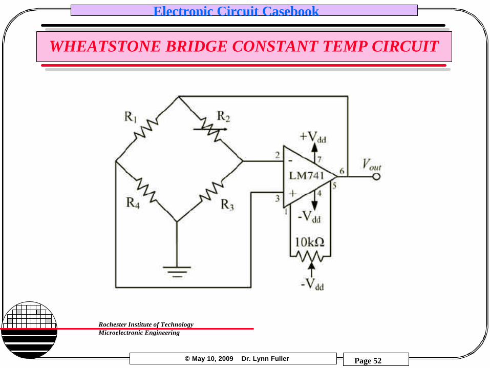
WHEATSTONE BRIDGE CONSTANT TEMP CIRCUIT

© May 10, 2009 Dr. Lynn Fuller
Electronic Circuit Casebook
Page 53
Rochester Institute of TechnologyMicroelectronic Engineering
DELTA CAPACITANCE TO AC VOLTAGE
Vin Cx
Vo If Cx is fixed Vo is zero. If Cx changes there will be a change in current and a corresponding change in Vo
Example: Let Vin = 3 volts, C = 10 pF, microphone action causes C to change by 0.1pF at 1000 Hz. Calculate the output voltage.
R

© May 10, 2009 Dr. Lynn Fuller
Electronic Circuit Casebook
Page 54
Rochester Institute of TechnologyMicroelectronic Engineering
CAPACITIVE OIL LEVEL DETECTION CIRCUIT
This circuit is designed to detect the presence of oil at a specified level. The fundamental operation is based on a threshold-crossing detection of signal level (voltage) due to a capacitive change of the probe. Contacting with different dielectric materials, either in air or immerging in oil, results in this change. As a consequence, the RC time constant of the probe is also altered, causing the probe to charge up to a different maximum voltage level within a given period of time. A peak detector is used to measure this voltage level, and the threshold-crossing detection is then carried out by the final stage op-amp, as shown.
100k
100k
4.7M
100p
3V
3V
3V
16M
2p – 3.5p
0.1µ
100k
220
LED
MC33204
1N4448100k
MC33204
MC33204
Jirachai Getpreecharsawas, 2009

© May 10, 2009 Dr. Lynn Fuller
Electronic Circuit Casebook
Page 55
Rochester Institute of TechnologyMicroelectronic Engineering
WIRELESS CAPACITANCE TO DIGITAL
CCLK
RCO____CCKEN______
0000000001
00000000
3 V
1 1
CCLR_____RCLK
RCLKSCLK
10-bit (Left) Shift Register
8-bitBinary Counter
Bluetooth SerialRF Link
CTS
TX
RX
RTS
2.4 kHz
5 Hz
5 Hz
Start Bit
Stop Bit
Internal Counter
000000 00 RC OscillatorSensor
RC Oscillator RC Oscillator
Jirachai Getpreecharsawas, 2008

© May 10, 2009 Dr. Lynn Fuller
Electronic Circuit Casebook
Page 56
Rochester Institute of TechnologyMicroelectronic Engineering
WIEN BRIDGE OSCILLATOR CIRCUIT
CMOS Analog Circuit Design, Phillip Allen, Douglas Holbert, Holt, Rinehard and Winston. 1987, pg 637-639.
STOPPLAY

© May 10, 2009 Dr. Lynn Fuller
Electronic Circuit Casebook
Page 57
Rochester Institute of TechnologyMicroelectronic Engineering
LOOP GAIN OF WIEN BRIDGE OSCILLATOR
CMOS Analog Circuit Design, Phillip Allen, Douglas Holbert, Holt, Rinehard and Winston. 1987, pg 637-639.

© May 10, 2009 Dr. Lynn Fuller
Electronic Circuit Casebook
Page 58
Rochester Institute of TechnologyMicroelectronic Engineering
LOW PASS FILTER
Vout
R2
-+
R1
C2
Vin
Derive an expression for Vo/VinPlot 20Log10 (Vo/Vin) vs frequencyVerify using SPICEVerify by building the circuit
Vo/Vin = -R2/R1 1
1 + j ω/ω1
ω = 2 π fω1 = 1/R2C2 f
1
SR2C2 + 1

© May 10, 2009 Dr. Lynn Fuller
Electronic Circuit Casebook
Page 59
Rochester Institute of TechnologyMicroelectronic Engineering
HIGH PASS FILTER
Vout
R2
-+
R1C1Vin
Derive an expression for Vo/VinPlot 20Log10 (Vo/Vin) vs frequencyVerify using SPICEVerify by building the circuit
Vo/Vin = -R2/R1 j ω/ω1
1 + j ω/ω1
ω = 2 π fω1 = 1/R1C1
f
SR1C1
SR1C1 + 1

© May 10, 2009 Dr. Lynn Fuller
Electronic Circuit Casebook
Page 60
Rochester Institute of TechnologyMicroelectronic Engineering
GENERAL FILTER
Vout-+
C2
Vin
R2C1R1
Derive an expression for Vo/VinPlot 20Log10 (Vo/Vin) vs frequencyVerify using SPICEVerify by building the circuit
Vo/Vin = -R2/R1 = -R2/R11 + j ω/ω1
1 + j ω/ω2
ω = 2 π fω1 = 1/R1C1, ω2 = 1/R2C2
SR1C1 + 1
SR2C2 + 1

© May 10, 2009 Dr. Lynn Fuller
Electronic Circuit Casebook
Page 61
Rochester Institute of TechnologyMicroelectronic Engineering
COMBINATIONS OF FILTERS
2nd Order low-pass, high-pass, bandpass, bandrejection and all pass filter
Vo/Vin = -R2/R1
Generalω1, ω2
Generalω3, ω4
Two General Filters in series1 + j ω/ω1
1 + j ω/ω2
Vo/Vin = -R2R4/R1R3 1 + j ω/ω1
1 + j ω/ω2
1 + j ω/ω3
1 + j ω/ω4

© May 10, 2009 Dr. Lynn Fuller
Electronic Circuit Casebook
Page 62
Rochester Institute of TechnologyMicroelectronic Engineering
SKETCH OF VARIOUS FILTER FREQUENCY RESPONSE
ω1 = ω3 < ω2 = ω4
ω2 = ω4 < ω1 = ω3
ω1 < ω2 < ω4 < ω3
ω2 < ω1 < ω3 < ω4
Vo/Vin = -R2R4/R1R3 1 + j ω/ω1
1 + j ω/ω2
1 + j ω/ω3
1 + j ω/ω4

© May 10, 2009 Dr. Lynn Fuller
Electronic Circuit Casebook
Page 63
Rochester Institute of TechnologyMicroelectronic Engineering
REFERENCES
1. Dr. Fullers webpage http://people.rit.edu/lffeee