Einführung in Hardware- und … • Lectures • Time ... Register-Transfer logic blocks, FSMs,...
44
Einführung in Hardware- und Systembeschreibungssprachen Prof. Dr. Miloš Krstić
Transcript of Einführung in Hardware- und … • Lectures • Time ... Register-Transfer logic blocks, FSMs,...
Einführung in Hardware- und
Systembeschreibungssprachen
Prof. Dr. Miloš Krstić

Digital Systems in Hardware –
Why is this important for informatics students?
• Digital systems are constituting devices around us.
2
2
kothamasusatish.blogspot.com

Design of Digital Systems–
Why is this important for informatics students?
• The main component of one informatic system is processor
• Processor is one example of the digital system
• It can be modelled with Boolean gates and memory
components
• We need to understand how the process of design and
modelling of a digital system work, and how digital system
operates
• If we understand this we will also understand how processor
works and how it can be designed
• This will enable also effective software development
• We will address also complex digital systems and the aspects
of its design 3

Goals of this Course
• Make the baseline of the knowledge of digital system and
hardware design
• Learn to use VHDL for digital system implementation
• Understand chip and FPGA design and test flow
• Get some information on the system level design flow and
SystemC modelling language
• Have hands-on experience with state-of-the-art CAD tools for
the design of digital systems
4

Plan
• Einführung Digitale Logik
• Einführung in HDL Beschreibungssprachen
Beispiel: VHDL
• ASIC & FPGA Designflow
• Test und Verifizierung digitaler Systeme
• System Design und TLM Modellierung
• Einführung in System-Level-Design-Languages
Beispiel: SystemC
5

Organisation
• Lectures
• Time: 14:00-16:00 Tue
Prof. Dr. Milos Krstic, IHP, Frankfurt (Oder) and University Potsdam
• Labs
• Time: 16:00-18:00 Tue
Dr. Steffen Zeidler, Anselm Breitentreiter
zeidler, breitenreiter @ihp-microelectronics.com
• During the semester we may have some swaps between lectures and
labs
6
Examination
• Examination will be oral
I will consist on set of small problems/exams to solve
Additionally, we will provide couple of theoretical questions
7

IHP in Frankfurt (Oder)

Literature
• Main resource
Mark Zwolinski, Digital System Design with VHDL, Prentice
Hall
For SystemC:
J. Bhasker, A SystemC Primer, Star Galaxy
Additionally there is a lot of material on the internet.
If support is required, please contact us!
9

Overview of this lecture
• Modern Digital Design
• CMOS Transistors & Logic Gates
Structure
“Switch-Level” Transistor Model
Some of the basic gates
• The VLSI Design Process
Levels of Abstraction
Design steps
Design styles
• VLSI Trends
• Design Examples
10
For this lecture the content was utilized from:
Presentation Complex Digital Systems, MIT USA
Presentation VLSI Circuit Design, John Nestor,
Lafayette College
Modern Digital Design
• Analogue and Digital circuit Design
• Digital Electronics is significant in consumer goods
Personal computers
Mobile phones
Tablets
• For design of Digital Electronics one needs CAD tools
synthesis
simulation
• Modelling in hardware description languages
VHDL
Verilog
11

Logic Gates
• Basic building blocks of digital circuit
component with one or more inputs and (usually) one output
inputs/outputs: 0 and 1
in reality are presented by voltage, for example 0V and 3.3V
• Integrated Circuit
Could be constituted with many logic gates
• Design Styles
ASIC and FPGA
12
Illustration: M. Zwolinski, Design of Digital Systems

• Custom and Semi-Custom
Hand-drawn transistors (+ some standard cells)
High volume, best possible performance: used for most advanced microprocessors, RF design
• Standard-Cell-Based ASICs
High volume, moderate performance: Graphics chips, network chips, cell-phone chips, automotive
• Field-Programmable Gate Arrays
Prototyping
Low volume, low-moderate performance applications
Different design styles require:
different design tools,
have different chip development cost,
and require different design time
VLSI Design Styles
13 Source: Complex Digital Systems, MIT USA

Full Custom Design Style
• Each circuit element is hand designed
• Tradeoffs
High Design Costs (enormous effort!)
High starting investment in production
High Performance
Low Unit Cost (good for high volume products!)
• Examples
Analog and Mixed-Signal
High-performance microprocessor
Design cost of a high-end CPU is on the order of $100 million
- this is why we pay so much for processor!
14
120 GHZ radar chip from IHP
Source: VLSI Circuit Design, John Nestor, Lafayette College

ASIC Design Style
• Pre-designed (or pre-manufactured) components that are assembled and wired by CAD tools.
Standard cell
pre-designed cells include: flip-flops, logic gates, IOs, etc.
• Tradeoffs
Low Design Cost
High starting investment in production
Medium Unit Cost – suboptimal design
Medium Performance (< 2 GHz with the current state-of-the-art technology)
• Examples:
Control chip for cell phone
Communication chip for phone or pads
Graphic accelerators
15
MW Switch
Source: VLSI Circuit Design, John Nestor, Lafayette College
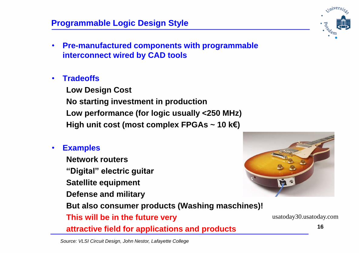
Programmable Logic Design Style
• Pre-manufactured components with programmable
interconnect wired by CAD tools
• Tradeoffs
Low Design Cost
No starting investment in production
Low performance (for logic usually <250 MHz)
High unit cost (most complex FPGAs ~ 10 k€)
• Examples
Network routers
“Digital” electric guitar
Satellite equipment
Defense and military
But also consumer products (Washing maschines)!
This will be in the future very
attractive field for applications and products 16
usatoday30.usatoday.com
Source: VLSI Circuit Design, John Nestor, Lafayette College

VLSI Technology Overview
• Commonly used technologies:
• CMOS* (Complementary Metal Oxide Semiconductor)
today dominant technology
Additionally present:
Bipolar (e.g., TTL)
Bi-CMOS - hybrid Bipolar, CMOS (for high speed, lower cost)
GaAs - Gallium Arsenide (for high speed, low noise, high cost)
Si-Ge - Silicon Germanium (for RF)
17
Source: VLSI Circuit Design, John Nestor, Lafayette College

Source: VLSI Circuit Design, John Nestor, Lafayette College
VLSI Levels of Abstraction
Specification (what the chip does, inputs/outputs)
System Level Modeling major resources, connections
Register-Transfer logic blocks, FSMs, memory, connections
Circuit transistors, parasitics, connections
Layout mask layers, polygons
Logic gates, flip-flops, latches, connections
18

VLSI Design Process
• Start from higher and
go to lower levels of
abstraction
• Use CAD tools to
automate parts of the
process
19
Library
New RTL Designs
HDL Top Module Definition
Simulation
Result OK?
Logic Synthesis
Simulation
Result OK?
Layout Synthesis
Simulation
Result OK?
Final Chip Layout
Test Benches
yes
Configurable Modules
(synthesizable RTL code)
+
Pre-defined Modules
New synthesis yes
yes
New layout run
sufficient?
yes
no
no
no
no
yes
no
Applications
System Specification

CMOS Transistors
29.05.2015. DCPS 2015 20
IN
GND
VDD
OUT
SP
SN
M1
M2
Metal Contacts
Poly-Si
P substrate
N well
P+ N+ N+ P+ N+
VDD GND OUT IN
P+
SN DN DP SP
PMOS (M2) NMOS (M1)
L L
Key feature:
transistor length L
2002: L=130nm
2003: L=90nm
2005: L=65nm
2008: L=45nm
2010: L=32nm
2012: L=22nm
2015: L=14nm
2016: L=10nm

CMOS Chip
21
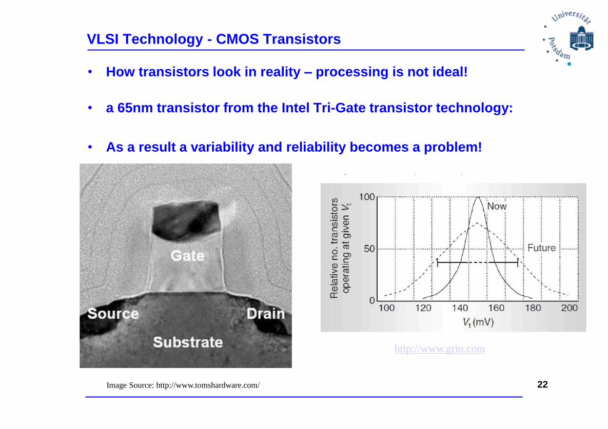
VLSI Technology - CMOS Transistors
• How transistors look in reality – processing is not ideal!
• a 65nm transistor from the Intel Tri-Gate transistor technology:
• As a result a variability and reliability becomes a problem!
Image Source: http://www.tomshardware.com/ 22
http://www.grin.com

Transistor Switch Model
• nfet or n transistor
on when gate H
"good" switch for logic L
"poor" switch for logic H
"pull-down" device
• pfet or p transistor
on when gate L
"good" switch for logic H
"poor" switch for logic L
"pull-up" device
23
L H
L L
L L
H L
H H
OFF when gate=H
ON when gate=L
OFF when gate=L
ON when gate=H

CMOS Logic Design
• Complementary transistor networks
Pullup: p transistors
Pulldown - n transistors
VDD
Out
Gnd
VDD
Out
Gnd
Pullup Network
(p-transistors)
Pulldown Network
(n-transistors)
InInputs
Inverter 24
sccs.swarthmore.edu

CMOS Inverter Operation
25
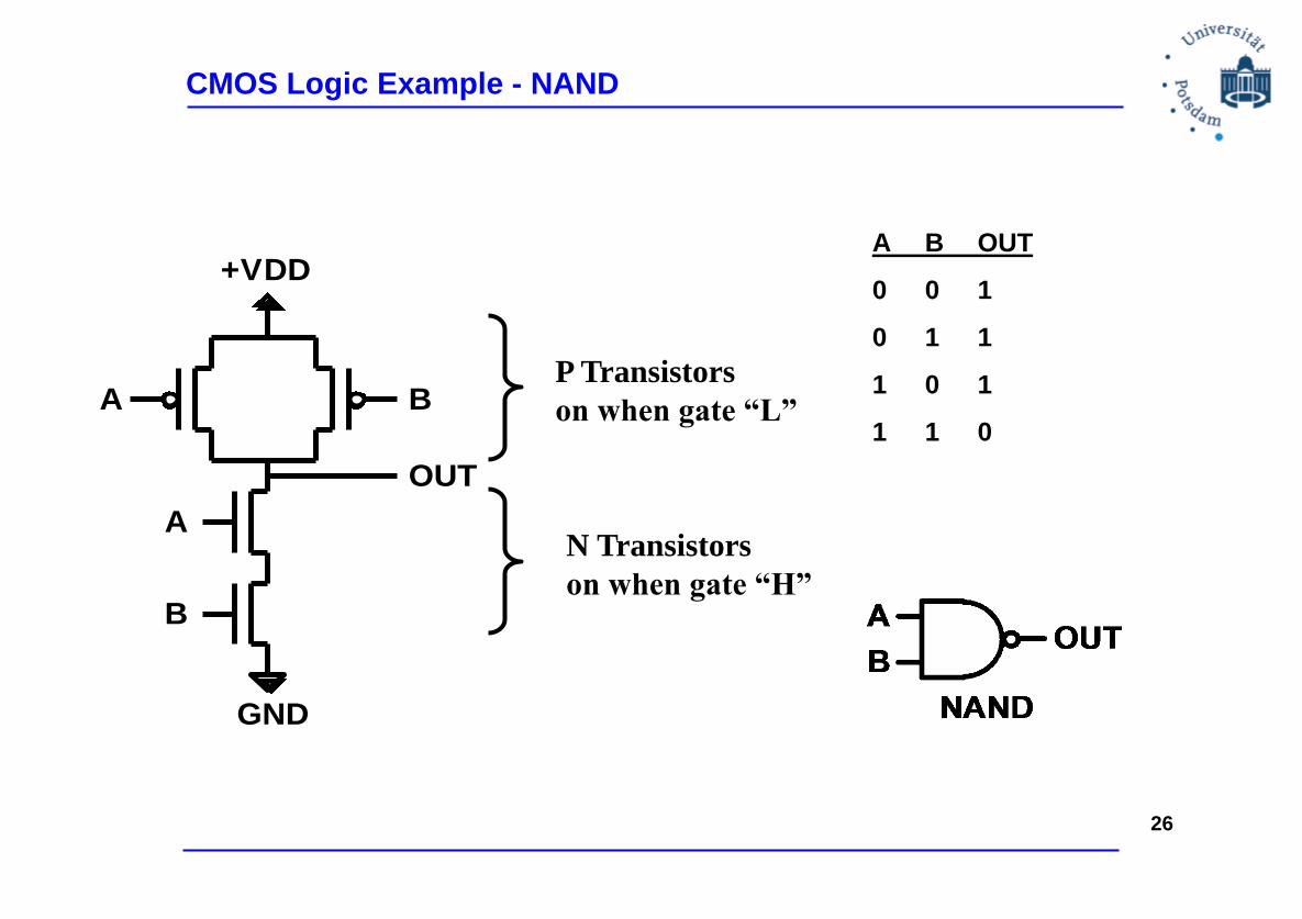
CMOS Logic Example - NAND
A B
A
B
OUT
+VDD
GND
P Transistors
on when gate “L”
N Transistors
on when gate “H”
26
A B OUT
0 0 1
0 1 1
1 0 1
1 1 0

VLSI Trends: Moore’s Law
• In 1965, Gordon Moore predicted that transistors would continue to
shrink, allowing:
Doubled transistor density every 18-24 months
Doubled performance every 18-24 months
• History has proven Moore right
• But, is the end is in sight?
Physical limitations (technology issues)
Economic limitations (new technology cost)
Gordon Moore
Intel Co-Founder and Chairmain Emeritus Image source: Intel Corporation www.intel.com
27
Source: VLSI Circuit Design, John Nestor, Lafayette College

Exponential growth: Moore’s Law
Intel 8080A, 1974
3Mhz, 6K transistors, 6u
Intel 8086, 1978, 33mm2
10Mhz, 29K transistors, 3u Intel 80286, 1982, 47mm2
12.5Mhz, 134K transistors, 1.5u
Intel 386DX, 1985, 43mm2
33Mhz, 275K transistors, 1u
Intel 486, 1989, 81mm2
50Mhz, 1.2M transistors, .8u
Intel Pentium, 1993/1994/1996, 295/147/90mm2
66Mhz, 3.1M transistors, .8u/.6u/.35u
Intel Pentium II, 1997, 203mm2/104mm2
300/333Mhz, 7.5M transistors, .35u/.25u
http://www.intel.com/intel/intelis/museum/exhibit/hist_micro/hof/hof_main.htm Shown with approximate relative sizes

Microprocessor Trends (Intel)
Source: http://www.intel.com/pressroom/kits/quickreffam.htm, media reports
Year Chip L transistors
1971 4004 10µm 2.3K
1974 8080 6µm 6.0K
1976 8088 3µm 29K
1982 80286 1.5µm 134K
1985 80386 1.5µm 275K
1989 80486 0.8µm 1.2M
1993 Pentium® 0.8µm 3.1M
1995 Pentium® Pro 0.6µm 15.5M
1999 Mobile PII 0.25µm 27.4
2000 Pentium® 4 180nm 42M
2002 Pentium® 4 (N) 130nm 55M
2003 Itanium® 2 (M) 130nm 410M
2004 Pentium® 4 (P) 90nm 125M
2006 Core 2 Duo® 65nm 291M
2009 Core I5® 45nm 774M
2010 Core I7® 32nm 1170M
2012 Core I7® - Ivy Bridge
22nm 1400M
2014 Broadwell 14nm 1900M
“Deep
Submicron”
29

Microprocessor Trends
Sources: arch.naist.jp
30
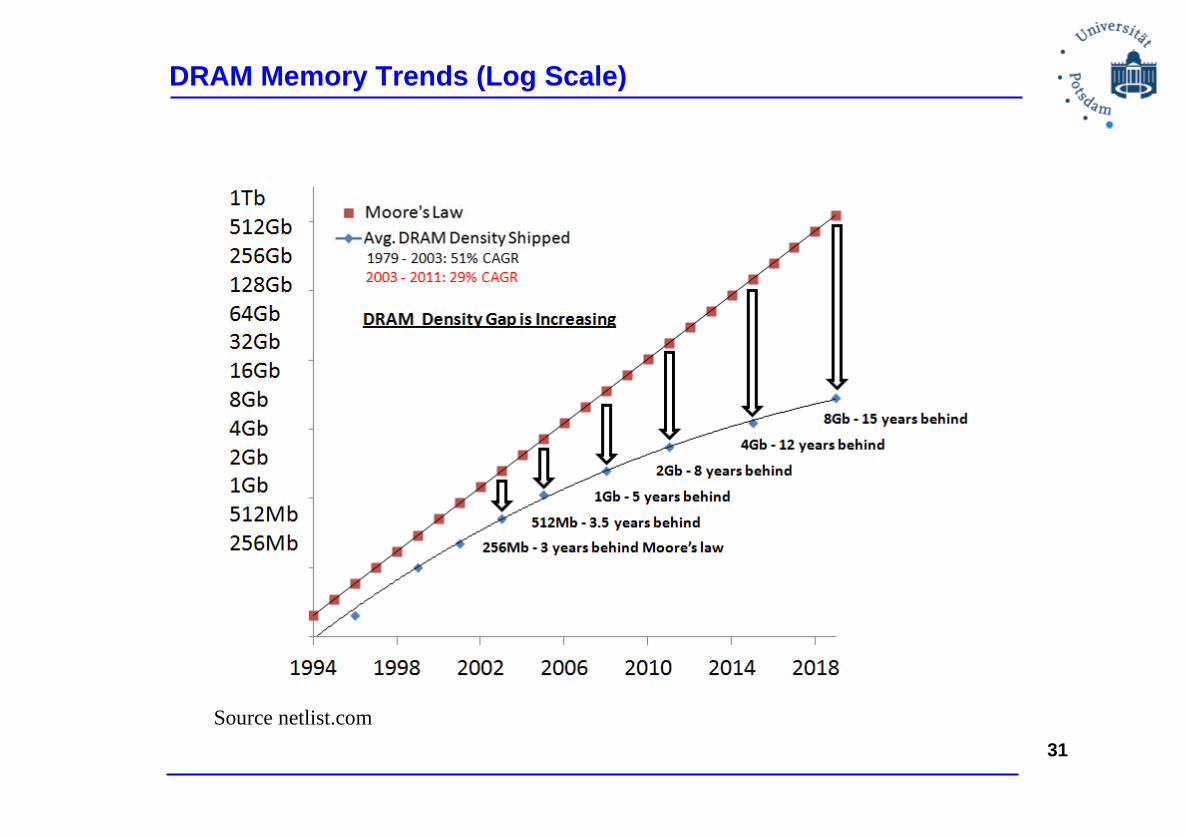
DRAM Memory Trends (Log Scale)
31
Source netlist.com

Processor Performance Trends
Source: http://www.gotw.ca/images/CPU.png
32

Summary - Technology Trends
• Processor
Logic capacity increases ~ 30% per year
Clock frequency increases ~ 20% per year
Cost per function decreases ~20% per year
• Memory
DRAM capacity: increases ~ 30% per year
(4x every 3 years)
Speed: increases ~ 10% per year
Cost per bit: decreases ~25% per year
Not any more!
33
Source: VLSI Circuit Design, John Nestor, Lafayette College

Design Effort is Growing Nvidia Graphics Processing Units
0
20
40
60
80
100
120
1993
1995
1996
1997
1998
1999
2000
2001
2001
2002
2002
Design Effort
per Chip
Transistors (M)
Relative staffing
on front-end
Relative staffing on
back-end
9x growth in
back-end staff
5x growth in
front-end staff
• Front-end is designing the logic (RTL)
• Back-end is placing the gates and routing the wires on the chip; meeting timing requirements; connecting power, ground, and clock – performing layout and verification
• New HL Tools are required! 34
Source: Complex Digital Systems, MIT USA

Design Cost Impacts Chip Cost An Altera study
• Non-Recurring Engineering (NRE) costs for a 90nm ASIC is ~ $30M
59% chip design (architecture, logic & I/O design, product & test engineering)
30% software and applications development
11% prototyping (masks, wafers, boards)
• If we sell 100,000 units, NRE costs add
$30M/100K = $300 per chip!
Alternative: Use FPGAs
Hand-crafted IBM-Sony-Toshiba Cell microprocessor achieves 4GHz in
90nm, but at the development cost of >$400M
35
Source: http://csg.csail.mit.edu/
Source: Complex Digital Systems, MIT USA

Gallery - Early Processors
Mos Technology 6502 Intel 4004
First µP - 2300 xtors
L=10µm
36 Image courtesy Intel Corporations
All Rights Reserved

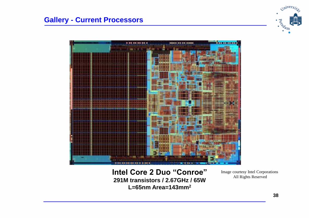
Gallery - Current Processors
Pentium® 4 42M transistors / 1.3-1.8GHz
49-55W
L=180nm
Pentium® 4 “Northwood” 55M transistors / 2-2.5GHz
55W
L=0.130nm Area=131mm2
Process Shrinks
Pentium® 4 “Prescott” 125M transistors / 2.8-3.4GHz
115W
L=90nm Area=112mm2
37 Image courtesy Intel Corporations
All Rights Reserved
Gallery - Current Processors
Intel Core 2 Duo “Conroe” 291M transistors / 2.67GHz / 65W
L=65nm Area=143mm2
Image courtesy Intel Corporations
All Rights Reserved
38

Intel Penryn (2007)
• Dual core
• Quad-issue out-of-order superscalar processors
• 6MB shared L2 cache
• 45nm technology
Metal gate transistors
High-K gate dielectric
• 410 Million transistors
• 3+? GHz clock frequency
Could fit over 500 486 processors on same size die.
Image courtesy Intel Corporations
All Rights Reserved

Intel Gulftown - I7 (2010)
• Min. feature size 32 nm
Cores 6 (physical), 12 (logical)
L2 cache 6 × 256 KB, L3 cache 12 MB
Front side bus replaced with QuickPath up to 6.4GT/s
TDP 130W
1.17 Bil. Transistors (240 mm2)
Up to 3.8 GHz clock frequency
40
Image courtesy Intel Corporations
All Rights Reserved
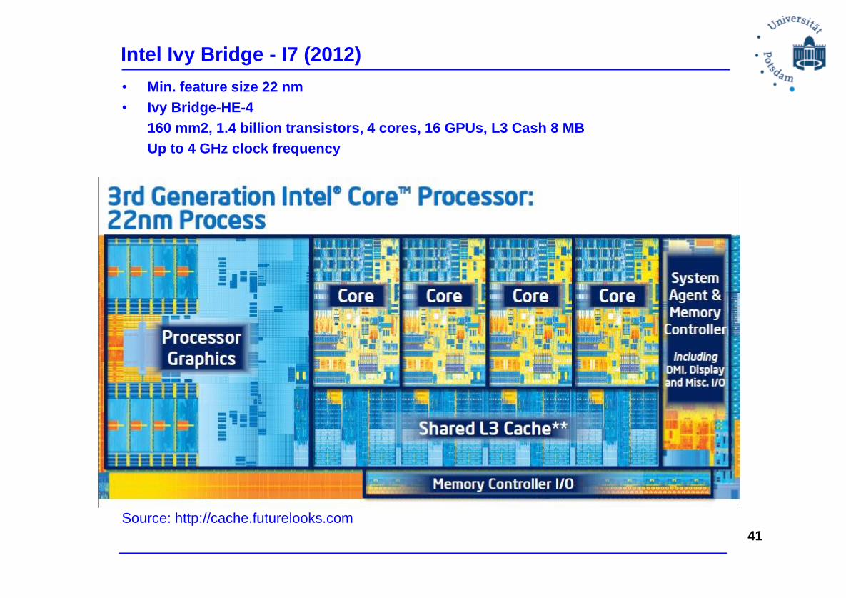
Intel Ivy Bridge - I7 (2012)
• Min. feature size 22 nm
• Ivy Bridge-HE-4
160 mm2, 1.4 billion transistors, 4 cores, 16 GPUs, L3 Cash 8 MB
Up to 4 GHz clock frequency
Source: http://cache.futurelooks.com
41

IHP’s Moonrake chip
• Moonrake Chip - GALS and synchronous OFDM gigabit transmitter for 60
GHz band
16M equivalent gates, 30% core logic;
218 memory: 8 FIFOs (64Kb), 86 SROMs (192Kb), 134 SRAMs (400Kb);
219 pads: 136 TX/shared pads, 20 NoC dedicated pads, 63 power pads.
TSMC 40-nm CMOS process;
4000µm2x2250µm2=9mm2;
LBGA-345 package;
Bondlib 55µm pitch.
42

SCREAMER Chip
25.04.2017 43
4 TSN hard-macros integrated on the same die (ASIC complexity~25mm2 in 130 nm CMOS)
Each macro is a secured wireless sensor node,
LEON-2 uProcessor and three crypto-cores (AES/SHA-1/ECC).
Different noise optimization techniques are used (current shaping, clock modulation, two-phase
clocking) MACRO 0f = 850MHz
MACRO 1f = 850MHz MACRO 2f = 850MHz
MACRO 3f = 850MHz
Substrate
noise
50 MHz 100 MHz 800 MHz 850MHz 900 MHz
MACRO 0
(dBm)
-32.85 -37.78 -60.82 -52.17 -59.04
MACRO1 (dB) -0.85 +0.45 -6.38 -5.74 -6.85
MACRO2 (dB) -4.77 -12.80 -5.63 -8.57 -7.14
MACRO3 (dB) -6.14 -1.93 -4.37 -2.54 -6.30
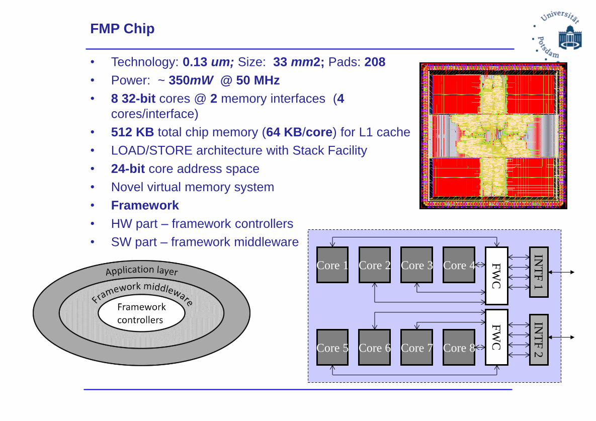
FMP Chip
• Technology: 0.13 um; Size: 33 mm2; Pads: 208
• Power: ~ 350mW @ 50 MHz
• 8 32-bit cores @ 2 memory interfaces (4
cores/interface)
• 512 KB total chip memory (64 KB/core) for L1 cache
• LOAD/STORE architecture with Stack Facility
• 24-bit core address space
• Novel virtual memory system
• Framework
• HW part – framework controllers
• SW part – framework middleware
Core 1
INT
F 1
IN
TF
2
Core 4 Core 2 Core 3
Core 5 Core 8 Core 6 Core 7
FW
C
FW
C