EEWeb Pulse - Issue 56, 2012
33
PULSE EEWeb.com Issue 56 July 24, 2012 Barry Katz President and CTO SiSoft Electrical Engineering Community EEWeb
description
Interview with Barry Katz - President and CTO of SiSoft; Simulating Large Systems with Thousands of Serial Links; Optimizing Your Next Temperature Measurement Configuration Part 2 - Thermocouples; Intersil Fisheye IC Lense Made Simple; RTZ - Return to Zero Comic
Transcript of EEWeb Pulse - Issue 56, 2012

PULSE EEWeb.comIssue 56
July 24, 2012
Barry KatzPresident and CTOSiSoft
Electrical Engineering Community
EEWeb

Contact Us For Advertising Opportunities
www.eeweb.com/advertising
Electrical Engineering CommunityEEWeb

EEWeb | Electrical Engineering Community Visit www.eeweb.com 3
TABLE O
F CO
NTEN
TSTABLE OF CONTENTS
Barry Katz SISOFT
Simulating Large Systems with Thousands 9 of Serial Links
Featured Products
Intersil Fisheye IC Lense Made SimpleBY JONPAUL JANDU WITH INTERSIL
RTZ - Return to Zero Comic 33
A detailed analysis of the virtual environment that is capable of both verifying connectivity and simulating any and all of the channels in large systems.
Interview with Barry Katz - President and CTO of SiSoft
How to take warped fisheye images and revert them to their normal rectiilinear picture format for real-world application.
An overview of several sources of temperature measurement error that are specific to thermocouples.
24
Optimizing Your Next Temperature Measurement Configuration -Part 2: Thermocouples
29
26BY ROBERT GREEN WITH KEITHLEY
BY BARRY KATZ, WALTER KATZ, MICHAEL STEINBERGER, DONALD TELIAN & SERGIO CAMERLO
4

EEWeb | Electrical Engineering Community Visit www.eeweb.com 4
INTERVIEWFEA
TURED IN
TERVIEW
How did you get into engineering and when did you start?I started my career at Digital Equipment Corporation (DEC) as part of the semiconductor group where I was part of a team responsible for writing system level signal integrity tools supporting the design of systems utilizing Alpha processors as well as other high-speed ASICs and supporting chipsets. In this role I was ultimately involved in the signal integrity of nearly every Alpha-based system ranging from workstations to high-end servers working with signal integrity engineers to deploy signal integrity tools and methodology on their projects.
SiSoft
BarryKatz
Will you tell us about your extensive experience in developing tools to integrate and automate a wide range of signal integrity analysis processes?Throughout my career, I have always had a focus on automation. This started with automated post-route crosstalk analysis tools and has led to tools for performing pre- and post-route integrated signal integrity, timing, and crosstalk analysis. My most recent efforts have been focused on serial link analysis where my team and I are focused on signaling at rates up to 28Gbps.
What have been some of your influences that have helped you get to where you are today? I’ve been very fortunate in this area. My father is an EDA pioneer and entrepreneur and has provided me guidance and mentoring throughout my career. The team of grad students and advisors I had the opportunity to work with at Carnegie Mellon University were also influential. The work I did at DEC both before and after forming SiSoft as well as the projects I have had the opportunity to work on at Ericsson, Cisco, Intel, and many other companies have
President and CTO

EEWeb | Electrical Engineering Community Visit www.eeweb.com 5
INTERVIEWFEA
TURED IN
TERVIEW
been influential. Lastly, my family. My wife and two boys are my rock and support me every day.
Do you have any tricks up your sleeve? I will tell you the key attribute that sets myself and my team at SiSoft apart. These days, the problems we SI engineers have to solve on a daily basis have become increasingly complex. Utilizing software tools to automate the solving of these problems has become a requirement. Many engineers will use these tools and accept the answers they get down to the 8th decimal point as gospel. My advice is don’t. Build an intuition of what you expect the answers to be and test that intuition. It’s almost like you are trying to predict the answer before you get it so that when you get the answer you can validate
What has been your favorite project?My favorite software development project has been the development of Quantum Channel Designer® (QCD), SiSoft’s Multi-Gigabit Serial Link Analysis Tool, which my team has been working on for five years now and will continue to develop into the future. Technology is moving so fast in this area with emerging standards and higher data rates, it keeps the work very exciting. On the hardware side, I have been fortunate to have the opportunity to collaborate with
some of our major customers on emerging products targeting the 4G LTE market. These designs exhibit
As a business, we are customer focused and will
remain focused on close collaborative relationships with systems designers
and their suppliers. We will continue
to work with these customers and their semi-
conductor vendors to ensure high quality, high-performance,
accurate models are available for
simulation of their systems.
complexity on an extreme scale in terms of speed, size and density.
Do you have any note-worthy engineering experiences? Every year you continue to grow and you have great experiences. In looking back at all of these, I do look back to a few noteworthy experiences. Our DesignVision award for QCD was one of the great accomplishments of our team at SiSoft. Of particular note this year was the work highlighted with Ericsson that we did on Virtual Prototype Analysis where we demonstrated automated post-route simulation on thousands of links in a large backplane system. Also, recently, was the work we did in driving the new IBIS-AMI modeling standard which is key to modeling the equalization and clock recovery of SerDes devices.
How do you continue to be actively involved with leading edge high-speed design?We are very lucky to have close collaborative relationships with our major system customers and semiconductor partners. It’s these relationships and working closely on current and next generation projects that enable us to stay ahead of the curve. We are working on the leading edge and solving tomorrow’s problems today. The credit goes to my team who always rise to the challenge and the rapidly changing landscape that is signal integrity.
I saw that you have played a key role in leading tool development efforts for SiSoft’s products. How have you done this? With any new product, standard, or capability, it always starts with a vision and recognition that
whether it makes sense. The other advice I would share with you is that whatever you do in life, maintain balance with work, family and hobbies.

EEWeb | Electrical Engineering Community Visit www.eeweb.com 6
INTERVIEWFEA
TURED IN
TERVIEW
taking that vision to product or implementation is a team effort and requires focus. The team often spans myself, my staff as well as customers and partners. We have done this multiple times at SiSoft on both large and small scales. Driving the vision to a shared vision with ownership from the team and a collaborative mindset are the keys.
Can you tell us more about SiSoft and the technology they are developing?
When SiSoft was formed, we largely started as a consulting services company working with companies including DEC, Compaq, HP, and Intel. I’ve always had a focus on automation so, to make our consultants more efficient, I hired my Dad and his former partner and
we developed tools for automating a lot of the HSPICE® simulation work we were doing. This led to the development of our first product SiAuditor™ and then Quantum-SI™ and Quantum Channel Designer®.
Will you tell us about SiAuditor, the first commercial software product that SiSoft launched?This was an exciting time for us at SiSoft. We were asked by Compaq to perform consulting services on a project that was spanning multiple groups and platforms with the potential for high-leverage between the SI analyses performed on these projects. I told them my team would do it, but that it had to be done using SiAuditor™, a new product we were in the process of developing and needed a project to implement it on. I guaranteed our success and, given our track record with those teams, they rolled the dice. We all did. The rest is history. That project
shipped on-time at speed. Compaq became the first user of SiAuditor, EMC followed shortly thereafter and we continued to roll.
How did this help change the dynamic of SiSoft as a company? This was the first of many steps in transitioning from a consulting services company with a few tools and scripts to a bona fide software company with a strong consulting services arm.
With technology changing at such a fast pace, what are a few of the main technologies that have helped your company in its growth and product development? • Enabling Scalable Simulation
Farms
• IBIS-AMI Modeling Standard
• Extraction – we don’t talk about simulating one net, we talk about simulation of all the nets.
How does SiSoft continue to provide award-winning EDA simulation software, methodology training and consulting services for system-level high-speed design?Close collaborative relationships with our customers and semiconductor partners. SiSoft’s consulting services group enables deep relationships and our ability to drive leading edge requirements back into our core technology.
What direction do you see your business heading in the next few years?As a business, we are customer focused and will remain focused on
close collaborative relationships
The need for greater and greater compute
resources is ever present. Companies
need a scaleable compute infrastructure
that enables their engineering teams to perform the required
simulations necessary for successful
product design.
with systems designers and their suppliers. We will continue to work with these customers and their semi-conductor vendors to ensure high quality, high-performance, accurate models are available for simulation of their systems. Whatever it takes to make them successful is where SiSoft will be.
What are some new technologies we can expect to see from SiSoft in the near future? As speeds get faster, you can expect expanded capability from SiSoft in the area of Repeaters/Retimers as well as support for emerging signaling standards. We are also looking to close the

EEWeb | Electrical Engineering Community Visit www.eeweb.com 7
INTERVIEWFEA
TURED IN
TERVIEW
communication gap between the SI engineers that are doing simulations and recommending system settings and the software engineers that are programming these settings in to registers in actual hardware. As simple as this may seem, many needless hours are spent debugging problems with this interface.
What challenges do you foresee in our industry?Compute infrastructure, mindset, and neural processing. The fact is that things are only going to get faster. Higher speeds mean more modeling and more simulation. The need for greater and greater compute resources is ever present. Companies need a scaleable compute infrastructure that enables their engineering teams to
perform the required simulations necessary for successful product design. There also needs to be recognition, by management, as to the importance of simulation and both active and passive model correlation and willingness to work with their EDA, interconnect and semiconductor vendors in collaborative ways to drive quality and capabilities. Simulation is not cheap, but it is worth it. Lastly, along the theme of neural processing, engineers need to build intuition through experience on trends or results they would intuitively expect in simulation and the lab and constantly be vigilant about validating their expectations. When there is a disconnect, drive it to closure. Video game engineering is not an option.
Is there anything that you have not accomplished yet, that you have your sights on accomplishing in the near future?I’ve been fortunate in my career to have the opportunity to do a lot of great things. As I reflect, I find that I enjoy both the engineering and business side of the equation. I look forward to the expansion of SiSoft and where that may lead us and I think longer term, I very much enjoy sharing my knowledge with other engineers so I see some sort of teaching in my future. On a personal level, like anyone else, I want to see my kids have their own successes in life and support them however I can. ■
Run 10's of 1,000's of Simulation Cases to Spot System-Level Trends.

Avago Technologies AEDR-850x three channel reflective encoders integrate an LED light source, photo detector and interpolator circuitry.
It is best suited to applications where small size and space matters!
Applications include medical hand held devices, camera phones, wheel chairs, actuator, vending machine applications, just to name a few.
www.avagotech.com/motioncontrol
© 2011 Avago Technologies. All rights reserved.
Avago Technologies Motion Control Solutions
World’s Smallest Miniature Reflective 3-channel Encoder
To request a free sample go to:
Features Advantages Benefits
3-channel encoding (AB and I)
Index Signal “I” No need for separate components to generate the index signal
Miniature size Surface mount leadless package: 3.95 mm (L) x 3.4mm (W) x 0.95mm H)
Ability to fit into miniature motor designs
304 LPI High encoding resolution Various CPR capable by adjusting to the matching ROP of the codewheel
Built in Interpolator of 1x, 2x, and 4x
1x, 2x and 4x via external pinouts
Base CPR resolution can be interpolated by end user
High operating frequencies: 55 kHz at 1x interpolation
Operating frequencies can be increased by external interpolator pinouts by maximum of 4x
Corresponding high RPM performance with increased frequencies
Index gating Options available for both gated and ungated versions
Catering for various user gating requirements
-20°C to 85°C Industrial application capable
Covering consumer, commercial and industrial applications

EEWeb | Electrical Engineering Community Visit www.eeweb.com 9
TECHN
ICA
L ARTIC
LETECHNICAL ARTICLE
Abstract While not long ago systems had only several serial links, it’s now becoming common for systems to include hundreds – and even thousands – of such links. This paper describes the development and analysis of a large system with thousands of serial links. Due to the system’s size and complexity, the design team invested in a multi-year effort to build and qualify a virtual environment capable of both verifying connectivity and simulating any and all of the channels. Problematic channels with incomplete system-level connections, poor eye openings, or high BER are quickly identified. Performance limiters such as inherent discontinuities (and their associated resonances), and Tx/Rx equalization imbalance are found and examined in detail. The virtual system is also used to guide design choices such as layer stacking, via construction, back-drilling, and trace/connector impedances. Processes to optimize and select
equalization choices are also described.
1. Introduction Pre-layout simulation has been demonstrated in [1] to explore the feasibility of proposed serial links as well
as their sensitivity to system variables. While exhaustive analysis of link performance against manufacturing variations is performed in [1] in a pre-layout context, this paper illustrates the advantages of an efficient post-layout (albeit, pre-hardware) environment capable of analyzing thousands of serial links in a reasonable amount of time. Specific link-level advantages include the ability to: (a) confirm system-level connectivity, (b) balance and optimize equalization, (c) quantify design margin against performance targets, and (d) identify discontinuity-induced resonances not found by pre-layout analysis. The fact that there is typically no other way to perform these tasks further underscores the value of analyzing a virtual system as detailed herein; a capability commonly referred to as Virtual Prototype Analysis or “VPA”.
The vision of VPA is to provide the ability to quantify electrical-layer performance of any or all of thousands of system-level links in a reasonable amount of time, pre-hardware. The authors are part of a larger team that has invested in a multi-year effort to enable the capabilities described. While post-layout analysis is not a new concept in the field of Signal Integrity (SI), high-speed serial links have brought significant changes in the way SI
Simulating LargeSystems withThousands ofSerial Links
Sergio Camerlo, EricssonDonald Telian, SiGuysMichael Steinberger, SiSoft
Barry Katz, SiSoftWalter Katz, SiSoft

EEWeb | Electrical Engineering Community Visit www.eeweb.com 10
TECHN
ICA
L ARTIC
LETECHNICAL ARTICLE
analysis is performed. In addition to the ability to simulate millions of bits, identifying and removing resonances and balancing equalization at the system level are just some of the significant process steps introduced by serial links and enabled by VPA. Once assembled, the virtual system further enables the examination of performance gains against design options. Since parameters such as back-drilling, connector choice/impedance, via construction, and layer ordering can be easily adapted, the system-level improvement of these cost-sensitive choices can be quantified without time-consuming hardware fabrication cycles.
Innovations achieved in the past decade have enabled VPA to be applied to thousands of serial links. Necessary model formats and simulation techniques (both convolution-based and statistical) capable of resolving 10-12 Bit Error Rates (BERs) and smaller have been well-documented elsewhere [2-5]. Instead, this paper addresses a significant barrier to deploying serial link analysis in a post-layout context: the ability to rapidly solve and simulate Printed Circuit Board (PCB) vias with sufficient accuracy. As such, attention is given to detailing recent advances made in via modeling. Furthermore, as mainstream data rates push above 5 Gbps there is little eye opening left at both the Rx pin and die [6]. At these data rates it is imperative to model and measure signal performance after Rx equalization is applied, as is now required by the majority of 3rd generation serial standards [7].
This paper illustrates VPA using a system of approximately 30 large-scale PCBs interconnected through a backplane fabricated with over 50 metal layers containing thousands of serial links ranging in length from about 12” to 36”. While the scale of this system is large, the concepts presented can be deployed in any system utilizing advanced high-speed serial link technologies.
Though data rates will continue to increase throughout this decade, the dominant trend will be “the parallelization of serial interfaces”. Indeed, the presence of thousands of serial links in a single system suggests the need to significantly scale our serial link analysis in width rather than frequency. The concepts presented herein are consistent with this theme.
2. Enabling Technologies Beyond basic serial link analysis capability, Virtual Prototype Analysis (VPA) of thousands of serial links at data rates beyond 5 Gbps has necessitated innovations detailed in this section. Specifically, these include:
1. The ability to quantify signal performance after the application of Rx equalization
2. Rapid generation and simulation of hundreds of via models with sufficient accuracy
3. Expanded capacity, throughput, and data mining capabilities
2.1 Post-equalized Rx Signal Performance The majority of 3rd generation serial standards verify serial link electrical performance (typically Tx, Channel, and Rx independently) at a location referred to as the “Rx Data Latch” or simply “Rx Latch” as shown in Figure 1. This change has been necessitated by the lack of an observable signal at the Rx pins and/or pad. Instead, modeled or “reference” Rx equalization is applied to the signal at the Rx pads to extract a signal with a measureable eye opening. Example standards now specifying reference Rx equalization (CTLE=Continuous Time Linear Equalizer and/or DFE=Decision Feedback Equalizer) include the higher data rate versions of SAS, USB, and many others [7].
This methodology shift has brought about changes in both Test & Measurement (T&M) equipment as well as simulators and models. Essentially, it is now necessary for T&M equipment to include “simulators” capable of post-processing a waveform captured at a measurement location that can be probed (such as the Rx pin) [8]. Similarly, simulators now handle increasingly complex Rx models capable of modeling the performance of the signal after it is recovered by Rx equalization. Whether these are models of component behavior provided by a
Figure 1: Typical Gigabit Receiver Showing Rx Latch
Tx CHANNEL Rx CTLE DFE
ClockRecovery
RxDataLatch
Gigabit Receiver

EEWeb | Electrical Engineering Community Visit www.eeweb.com 11
TECHN
ICA
L ARTIC
LETECHNICAL ARTICLE
silicon vendor or modeled “reference” behavior provided by a tool or standard, they are increasingly available as executables in the AMI (Algorithmic Modeling Interface) format defined in the IBIS 5.0 specification [13].
2.2 Compact and Efficient Via Models To support the comprehensive analysis of systems containing thousands of serial links, via modeling must satisfy three primary requirements:
1. Computation of via models for many different via geometries must be practical.
2. The via models must solve and simulate quickly.
3. The via models must correlate to measured data.
The approach detailed herein is based on previously published papers that compare via models to measured data [9], [10]. Both papers conclude that vias behave like TEM transmission lines whose impedance can be calculated by assuming that there is a continuous shield at the edge of the antipad and running parallel to the via barrel (i.e., in the direction of the board thickness). [10] offered a motivation for this approximation by hypothesizing that radial TEM waves propagating from the edge of the antipad produced magnetic fields that approximately cancel the magnetic field from the via barrel. So far, this still appears to be a good approximation and explanation.
The via model deployed herein adds an equivalent circuit for the top and bottom pads and the exit trace to the transmission line described in [9] and [10]. This equivalent circuit is the combination of a few lumped and distributed elements, with element values derived primarily from physical properties. The model is accurate for single ended and common mode as well as differential mode. Since this equivalent circuit is relatively simple, it takes very little time to derive the model and compute its response.
[9] observed that the vias appeared to be longer electrically than one would have predicted based on the via length and the dielectric constant of the board. The explanation offered was that the effective dielectric constant for waves flowing in the direction of the board thickness was higher than that for waves flowing in the plane of the board. Further text can be found in [11].
To test the via length hypothesis advanced in [9], we extracted the insertion phase for the measured data for [10]. We also calculated the insertion phase predicted by our closed form model equations with the assumption that the dielectric constant is isotropic. Insertion phase is related to dielectric constant in that:
1. The dielectric constant determines the propagation velocity in the structure.
2. The group delay of the structure is the physical length of the structure divided by the propagation velocity.
3. The insertion phase is the integral of the group delay with respect to the angular frequency.
As shown in Figure 2 and the modeled and measured phase data from the Simple Via Experiment [10], the data supports the hypothesis of an isotropic dielectric constant rather than an anisotropic one because the dielectric constant determined from propagation in the X and Y directions is consistent with the delay in the Z direction.
It therefore appears that a different hypothesis is required to explain the unexpected measured electrical length of vias. To create the via model used herein, we measured pad to pad S parameters for numerous differential traces on an unpopulated backplane. Each trace measured consisted of a differential via, a differential backplane trace, and another differential via.
The analysis approach was to convert the measured S parameters to Time Domain Reflectometry (TDR) plots and measure the electrical length of the via at the beginning of the trace in both single ended and
Figure 2: Modeled and Measured Phase from Simple Via Experiment
Frequency
Inse
rtio
n P
ha
se (r
ad
ian
s)
0 2E+09 4E+09 6E+09 8E+09 1E+10 1.2E+10 1.6E+10 1.8E+10 2E+101.4E+10
-1.6
-1.4
-1.2
-1
-0.8
-0.6
-0.4
-0.2
0
0.2
0.4
Meas 1
Meas 2
Model
EEWeb | Electrical Engineering Community Visit www.eeweb.com 12
TECHN
ICA
L ARTIC
LETECHNICAL ARTICLE
differential modes. Since the measurement was made from pad to pad, the launching via was the very first element in the electrical path, so relatively precise measurements could be made. The measurement bandwidth was 20GHz, producing an effective TDR rise time of 17pS.
The measured electrical length vs. physical length is shown in Figure 3. In this Figure, the single ended measurements are shown using yellow symbols and the differential measurements are shown using red symbols. A line is extended through the measured differential values.
The line in Figure 3 was drawn through the differential mode data points because they show less spread than the single ended data points, and also because differential mode is not affected by the ground return impedance.
The slope of the line in Figure 3 corresponds to a dielectric constant of 3.61, compared to a dielectric constant of 3.41 for the traces on this particular PC board. This difference is within experimental error.
Figure 3 indicates that the increased length appears to be a constant length offset of about 0.05” rather than a decreased propagation velocity. This offset can be explained by considering the path the current must follow.
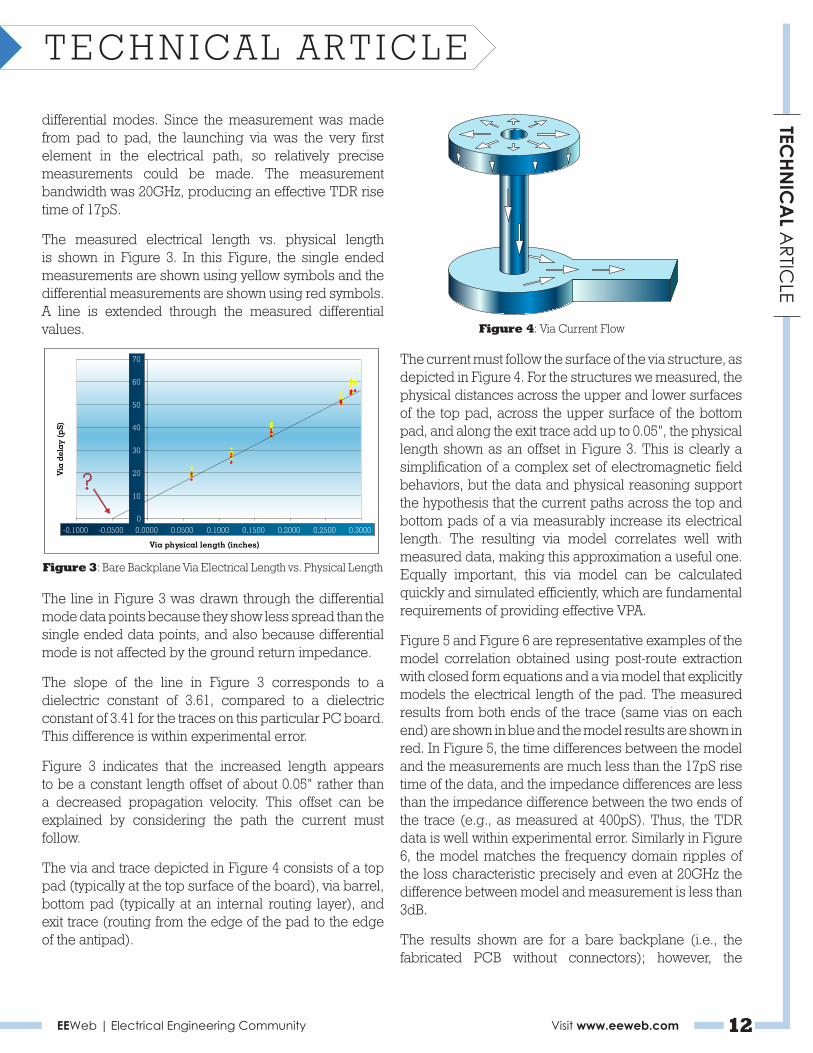
The via and trace depicted in Figure 4 consists of a top pad (typically at the top surface of the board), via barrel, bottom pad (typically at an internal routing layer), and exit trace (routing from the edge of the pad to the edge of the antipad).
The current must follow the surface of the via structure, as depicted in Figure 4. For the structures we measured, the physical distances across the upper and lower surfaces of the top pad, across the upper surface of the bottom pad, and along the exit trace add up to 0.05”, the physical length shown as an offset in Figure 3. This is clearly a simplification of a complex set of electromagnetic field behaviors, but the data and physical reasoning support the hypothesis that the current paths across the top and bottom pads of a via measurably increase its electrical length. The resulting via model correlates well with measured data, making this approximation a useful one. Equally important, this via model can be calculated quickly and simulated efficiently, which are fundamental requirements of providing effective VPA.
Figure 5 and Figure 6 are representative examples of the model correlation obtained using post-route extraction with closed form equations and a via model that explicitly models the electrical length of the pad. The measured results from both ends of the trace (same vias on each end) are shown in blue and the model results are shown in red. In Figure 5, the time differences between the model and the measurements are much less than the 17pS rise time of the data, and the impedance differences are less than the impedance difference between the two ends of the trace (e.g., as measured at 400pS). Thus, the TDR data is well within experimental error. Similarly in Figure 6, the model matches the frequency domain ripples of the loss characteristic precisely and even at 20GHz the difference between model and measurement is less than 3dB.
The results shown are for a bare backplane (i.e., the fabricated PCB without connectors); however, the
Figure 3: Bare Backplane Via Electrical Length vs. Physical Length
Figure 4: Via Current Flow
Via physical length (inches)
Via
del
ay
(pS
)
?
0
10
20
30
40
50
60
70
-0.1000 -0.0500 0.0000 0.0500 0.1000 0.1500 0.2000 0.2500 0.3000

EEWeb | Electrical Engineering Community Visit www.eeweb.com 13
TECHN
ICA
L ARTIC
LETECHNICAL ARTICLE
correlation is almost as good when connectors and cards are added.
As demonstrated by Figures 5 and 6, this via model is more than adequate for analyses up to 10 Gbps, and provides useful results up to 20 Gbps. In the future, it could be improved by providing direct computation of the few remaining heuristic element values, and by explicitly calculating the coupling of vias to each other and to the ground plane cavity.
2.3 Capacity, Throughput, and Data Mining Analyzing the behavior of a complete system requires that the VPA environment be able to process a fully populated virtual system model. This model may include dozens of PCB databases, totaling as many as 250,000 nets and 1,000,000 pins. A single post-route simulation run can require up to 25,000 simulations and generate 250,000 simulation files. The simulator’s analysis engine and database must scale to these levels and still provide reasonable performance.
Post-route simulations must be performed quickly
enough to provide useful feedback to the PCB layout team. This means taking periodic PCB database revisions, performing simulations, interpreting results and providing updated physical design rules within 48 hours. Allowing a day for interpretation of results and updating design rules, that leaves a day for setting up and performing the post-route simulation run. The simulation tool must be able to extract post-route topologies automatically, generate via models on-the-fly, and construct connector models from slice data provided by the connector manufacturer. Given the size of the simulation task, turnaround time is reduced through the combination of Statistical modeling techniques (a Statistical simulation will run in seconds, while its Time-Domain equivalent may take 50-500x longer) and acceleration though parallel processing (server farms). The simulation environment must automate the process, since complexity is high and repeatability is key to ensuring quality, as VPA will be repeated many times throughout the course of the design.
Once the simulations are complete, it can be difficult to see “the forest for the trees”. It’s not enough to produce massive sets of raw simulation data, since the data needs to be analyzed and updated design rules created
Figure 5: Typical Differential TDR Correlation Result
Figure 6: Typical Differential Insertion Loss Correlation Result
100.0
90.0
80.0
70.0
60.0
0.0 100.0 200 0.0 300.0 400.0 500.0 600.0
Ohm
s
Time (ps)
-10.0
-5.0
0.0
-15.0
-20.0
-25.0
-30.0
-35.0
0.0 5.0 10.0 15.0 20.0
DB
Hertz (GHz)

EEWeb | Electrical Engineering Community Visit www.eeweb.com 14
TECHN
ICA
L ARTIC
LETECHNICAL ARTICLE
quickly. Productivity is increased when simulation output includes key performance metrics like eye height and width for each simulation case, associated with the physical characteristics of each channel. Organizing the results allows the designer to scan the data for best and worst case conditions, as well as overall trends and “outliers” that will require a more thorough investigation. There are two important aspects to post-route simulation data mining: automated reporting and interactive drill-down of results.
Automated reporting provides the first level of analysis and includes reports like:
• Electrical integrity checks: connectivity, polarityswizzles, Tx/Rx compatibility
•Physicalcharacteristics:Netlengths,lengthsbylayer,potential resonant conditions
• Standards compliance: insertion loss, return loss,crosstalk ratio, eye mask pass/fail
• Performance metrics: Eye height, eye width, BER,optimized EQ settings
•Automaticidentificationofbest/worstcasecasesandassociated design variables
Once areas are identified for further investigation, problems are isolated by drilling down into individual simulation cases and performing what-if simulations to explore potential solutions. Important capabilities include:
• Correlate design metrics as a function of designvariables or other performance metrics
•Correlate anywaveform at any node in the network(including physically inaccessible nodes)
•Overlaycompliancemasksonsimulationplots
•Editpost-routetopologiestosupportinteractivewhat-ifanalysis
Providing these capabilities in a way that provides reasonable turnaround with currently available computers is a tall order, but this is the problem that needs to be solved to enable full-system analysis.
3. Virtual Prototype Analysis This section details system-level capabilities enabled by VPA that both verify interconnect integrity and optimize signal integrity.
3.1 Connectivity The value of the virtual system’s ability to confirm system-level connectivity – or, interconnect integrity – can not be overstated. While schematic/PCB netlist forward and backward annotation capabilities ensure connectivity at a single PCB level, the virtual system confirms connectivity at the system level. Furthermore, as new PCBs are developed or existing PCBs are revised they are verified in the virtual system to confirm interconnect integrity and link performance prior to fabrication. In other words the virtual system can serve as a “test-bench” that verifies that new PCBs, perhaps developed by remotely located teams in different geographies and time zones, will perform as expected when plugged into the real backplane.
Interconnect integrity can be verified physically, electrically, and operationally, and examples of each method are provided below on a typical virtual system.
Physical connectivity for hundreds of differential pairs is confirmed in the Figure 7 which plots the combined driver to receiver length of signals spanning three PCBs (card, backplane, card). Thousands of signals are shown on the X axis versus each signal’s length on the Y axis in inches. The distribution of backplane net lengths is shown in red, and the corresponding total length of each pair is plotted in green. The fact that total length always exceeds backplane length provides the first level of confirmation that all signals connect from the Tx on one card across the backplane to the Rx on another card. Markers further quantify the distribution of PCB lengths, in this case revealing there are 518 nets with backplane lengths between 8” and 16”, 318 nets with lengths between 16” and 24”, and so on.

EEWeb | Electrical Engineering Community Visit www.eeweb.com 15
TECHN
ICA
L ARTIC
LETECHNICAL ARTICLE
While the data above suggests all nets are connected across the boards, we are only viewing their combined length. The plots in Figure 8 go one step further and show the differential insertion loss (left) and their associated fitted attenuation (right, an averaging of the insertion loss) of thousands of channels against typical industry masks in black. This confirms the nets are connected electrically, and demonstrates the range of system-level insertion loss we can expect to compensate for at various frequencies of operation.
Plotting mask margins against channel loss in Figure 9 reveals that higher-loss channels slightly violate the mask (at very low frequencies, per the plot above right). In the plot below, red is insertion loss margin to mask and blue is the margin of the fitted attenuation to the mask.
With a good sense of electrical connectivity, we next examine operational connectivity by confirming that all nets produce an eye opening with typical equalization as shown in Figure 10 (eye height in red and width in blue). The eye openings recorded have a 10-12 probability of
Figure 8: Electrical Connectivity--Insertion Loss & Fitted Attenuation
occurring, and hence are related to a certain BER as defined by the Rx characteristics.
As two of the channels show no eye height or width (extreme right Figure 10) it’s possible these channels are not operating or simulating correctly. Various methods shown below exist to build confidence that those nets are simulating and producing meaningful results. At
left in Figure 11 we overlay hundreds of bathtub curves and confirm that two nets fail to yield an eye below a probability of 10-11 (highlighted in red), and hence show
Figure 7: Physical Connectivity - Backplane and Total Net Lengths
Figure 9: Insertion Loss and Fitted Attenuation Margins to Mask
Figure 10: Operational Connectivity - 10-12 Eye Heights and Widths
35.0
40.0
30.0
25.0
20.0
0.20 0.40
0.326k 0.845k 1.163k
38.120
24.0
16.0
8.0
.060 0.80 1.0 1.20
15.0
10.0
5.0
Leng
th
Row (k)
x2: (0.844k)
x1: (0.326k)
MEDUIM
dx: 0.518k
SDD21 Insertion Loss (dB)
DB
2.0
1.50
1.0
0.50
0.00.0
-0.50
-15.0 -14.0 -13.0 -12.0 -11.0 -10.0 -9.0 -8.0 -7.0 -6.0
Vo
lts
(mV
)
Tim
e (p
s)
160.0
170.0
140.0
120.0
100.0
0.20 0.40 0.60 0.80 1.0 1.20
80.0
60.0
40.0
20.0
0.0
80.0
70.0
60.0
50.0
40.0
30.0
20.0
10.0
0.0

EEWeb | Electrical Engineering Community Visit www.eeweb.com 16
TECHN
ICA
L ARTIC
LETECHNICAL ARTICLE
a closed eye at 10-12 probability in Figure 10. At right the statistical eye for these two nets confirms they do produce an eye at lower probability, yet - for reasons to be explained later - are less stable than the others.
Additional operational connectivity tests include plotting all pulse responses in Figure 12 (at left) and eye parameters at 10-3 probability (at right, height in red, width in blue). The pulse responses reveal the range of channel delays and their corresponding attenuation,
as well as a few nets with p/n reversal or “swizzle” (i.e., those nets with a negative-going pulse response). The 10-3 probability simulations demonstrate much wider eye openings than the 10-12 plot shown in Figure 10, which further confirms VPA is operationally functioning as expected.
With connectivity and functionality confirmed, we are in position to extract design margins and resolve poorly performing channels prior to fabricating hardware.
3.2 Design Margins The previous section has demonstrated that hundreds of thousands of datapoints have been generated for further examination during the design process. To illustrate this process, this section will focus on extracting and analyzing design margins measured on a cluster of links with medium length (around 20”) and moderate levels of equalization. Electrical performance will be judged by examining 10-12 eye heights and widths measured at the Rx die prior to equalization, while the gains of balancing system-level equalization will be addressed in a later section.
Figure 13 plots eye height on the Y axis versus eye width on the X axis for hundreds of differential pairs. The plot at left reveals that the majority of the signals cluster around 70mV/70pS eye height/width, yet a few of the signals have eye openings below 50mV/50pS. The plot at right presents the same data while delineating the direction of signal transmission into two different colors, red and blue. This plot reveals that, while many of the blue signals perform quite well, all of the signals below 50mV/50pS are transmitting in the blue direction.
Recognizing that the worst eye heights also have the worst widths, the plots in Figure 14 allow us to study performance by plotting eye height on the X axis against system variables on the Y axis. The plot at left shows eye height versus backplane layer revealing that, in general, signals on deeper layers perform worse than those on upper layers. The plot at right shows eye height versus connector row, revealing that the worst performing signals utilize row 6 in the connector.
Figure 11: Operational Connectivity - Bathtub Plots and High BER Eyes
Figure 12: Operational Connectivity - Pulse Responses and 10-3 Eye Parameters
200.0
-200.0
3.0 4.0
Time (ns)
5.0 6.0 7.0 8.0
-100.0
100.0
0.0
Vo
lts (
mV
)
200.0
250.0
110.0
100.0
90.0
80.0
70.0
150.0
100.0
0.20 0.40 0.60 0.80 1.0 1.20
50.0
0.0
Row (k)
Vo
lts (
mV
)
Tim
e (
ps)

EEWeb | Electrical Engineering Community Visit www.eeweb.com 17
TECHN
ICA
L ARTIC
LETECHNICAL ARTICLE
corners as annotated above the graph. Eye heights are plotted at three different probabilities (implying three different BERs) delineated in red, green, and blue. This
The data above allows us to hypothesize that the worst case nets in this length bundle are those with the following attributes:
1. signals driven in the blue direction in Figure 13
2. signals routed on the lowest (“deepest”) backplane layers
3. signals connected through connector row 6
To test this hypothesis against signals with short, medium, and long backplane lengths in Figure 15 we plot all signal bundle eye height/widths below in blue and superimpose the subset of nets with these attributes in red. These plots confirm that nets with these characteristics describe the nets with the poorest performance.
Thus far we have demonstrated the value of extracting thousands of performance estimates for all signals in the system, and how these datapoints can be filtered to identify which signals perform poorly. The process shown illustrates the value of quantifying specific net-level performance across the system during a stage of development when design adjustments can be more easily made. The specific phenomenon identified above will be explained in more detail in the next section on discontinuity-induced resonance.
Link performance should also be plotted against both corner-case behaviors and decreasing BER, as shown in Figure 16. In this Figure, nine corners are created by combining three silicon corners with three interconnect
plot indicates that there is a significant change in design margin as we vary silicon and interconnect corners, as is evident by viewing any vertical slice in the Figure.
3.3 Discontinuity-Induced Resonances Using typical fabrication technologies, it’s not uncommon for the primary channel discontinuities to exist at component and connector locations due to their associated vias. Figure 17 shows a measured (red) and simulated (green) differential TDR plot of a typical (non-
optimized) channel measured from the Tx to Rx. While much of the channel’s response is fairly flat around 100 Ohms impedance, the backplane connector locations are quite visible at ~1 nS and ~4 nS. Even though the impedance of the connector itself is roughly 100 Ohms, the connector vias create the two lower impedance dips on either side of the connector transition.
The presence of lower-impedance vias on both sides of the connectors cause a signal disturbance whose length is defined by the delay through the connector. The discontinuity causes some portion of the waves traveling
Figure 13: Eye Height vs. Eye Width, with Signal Direction
Figure 14: Eye Height vs. Backplane Layer and Connector Row
Figure 15: Channels with Least Margin Consistent Across Signal Lengths
Figure 16: Corner Case Design Margins with Decreasing BER
Vo
lts (
mV
)
150.0
100.0
50.0
0.0
50.040.030.0 60.0 70.0 80.0 90.0
Stat Eve Width (ps) (p) Stat Eve Width (ps) (p)
50.040.030.0 60.0 70.0 80.0 90.0
0.0
Vo
lts (
mV
)
150.0
100.0
50.0
Stat Eve Width (ps) (p) Stat Eve Width (ps) (p) Stat Eve Width (ps) (p)
Vo
lts
(mv)
30.0
160.0
140.0
120.0
100.0 100.0
150.0140.0
180.0
160.0
120.0
100.0
80.0
60.0
40.0
20.0
0.0
50.0
0.0
80.0
60.0
40.0
20.0
40.0 50.0 60.0 70.0 80.0 30.0 40.0 50.0 60.0 70.0 80.0 90.0 40.0 50.0 60.0 70.0 80.0
FFFE
400.0
300.0
200.0
100.0
0.0
0.0 100.0
Row
200.0 300.0 400.0
FFSE FFTE SSFE SSSE
y1: (394.10mV)y2: (143.20mV)dy: (250.90mV)
SSTE TTFE TTSE TTTE
Vo
lts
(mv)
Un
itle
ss (
y) 40.0
30.0
20.0
50.0
10.0
60.040.020.0 100.080.0 120.0 140.0 160.0
Stat Eve Height (V) (m)
60.040.020.0 100.080.0 120.0 140.0 160.0
Stat Eve Height (V) (m)
Un
itle
ss
4.0
3.0
2.0
5.0
6.0
1.0

EEWeb | Electrical Engineering Community Visit www.eeweb.com 18
TECHN
ICA
L ARTIC
LETECHNICAL ARTICLE
through the connector to reflect off the 2nd via and return to their source. As the energy is reflected back, some
included in the analysis, since they impose additional time delay as well.
portion reflects off the 1st via back into the connector, where again a portion will reflect back off the 2nd via and so on. This disturbance of defined length and the energy trapped in the structure can be referred to as a “discontinuity-induced resonance” or “standing wave”.
To better understand the discontinuities related to the connector vias, we must first quantify the delays through the various rows of the connectors. Placing a model of each row in the center of an ideal transmission line the Time Domain Transmission (TDT) plot in Figure 18 reveals the delays for each row, which are tabularized in Table 1.
As Table 1 shows, the standing wave (or roundtrip) frequencies suggest all rows longer than row 3 are within the range of 6 Gbps frequencies. However this explanation is focused on the connector only, while the problematic discontinuities also include via structures on both sides of the connector. These vias must be
Figure 18: TDT of Connector Rows
A study of the various connector vias reveals that longest via delays are about 20pS on the cards and 60pS on the backplane. Combining these and counting half the via transit time to be within our problematic structure, in Table 2 we find that the row 6 delay is ~2 UI and hence energy from double-bit (and a portion of single-bit) patterns will resonate and degrade performance, as shown previously in the section on design margins.
Further analysis shows that if a connector structure of this length is used it is helpful if at least one of the discontinuities on either side is removed. This lengthens the structure giving it more loss and therefore less pronounced standing waves. Solutions such as lower impedance traces and connectors and/or the use of specialized via structures can be used to smooth the discontinuities surrounding a connector. While pre-route analysis endeavors to exhaustively explore many connector/via
combinations and other channel discontinuities, VPA has the potential to isolate combinations that may not have been comprehended previously prior to assembling the virtual prototype of the larger system.
3.4 System-level Equalization While Tx equalization has been common since ~2 Gbps, the increasing presence of Rx equalization and models of the same enables system-level equalization optimization and balancing between the Tx and Rx. And, as this section will demonstrate, important performance gains can be realized by doing so.
Knowledge of the data stream enables a Tx to implement pre-cursor equalization, while an Rx can implement only post-cursor equalization. As such, we can hypothesize
Figure 17: Measured (red) and Simulated (green) Channel TDR Showing Discontinuities
Table 1: Connector Row Delays
Table 2: Combined Connector and Via Delays
110.0
100.0
90.0
80.0
70.0
60.0
0.0 1.0 2.0 3.0 4.0 5.0 6.0
Oh
ms
Time (ns)
Vol
ts (V
)
Time (ps)
1.20
1.0
0.80
0.60
0.40
0.20
0.0
2100.0 2150.0 2200.0 2250.0 2300.0 2350.0
2107.0ps 2273.0ps

EEWeb | Electrical Engineering Community Visit www.eeweb.com 19
TECHN
ICA
L ARTIC
LETECHNICAL ARTICLE
it would be best to let the Rx handle the post-cursor to preserve as much Tx amplitude swing as possible. Conversely, since the Tx is the only device capable of performing pre-cursor equalization, it should be tasked with handling pulse spreading during those bit times. The Tx may also be tasked with post-cursor equalization if the system requires more than the Rx can provide.
Using simulation to test this hypothesis, Figure 19 examines the performance of a typical net when sharing post-cursor equalization between the Tx and Rx. All eye openings are plotted at the Rx Latch with a small amount of Tx pre-cursor (-10%) and Rx CTLE applied. In the eye at left, the Tx has fully equalized the signal leaving little room for contribution from the Rx DFE. At center we evenly divide post-cursor equalization between the Tx (17%) and the Rx (18%). In this scenario the Tx eye is increased ~100mV suggesting that the extra energy delivered by the Tx is helpful. At right we see the eye shape when the Tx has only pre-cursor equalization and the Rx DFE’s post-cursor is at -32%. This scenario increases the eye height another 170mV at the Rx Latch, and the eye width has improved as well. From scenario 1 to 3, the eye opening has improved by 100% simply by deploying a system-level view of channel equalization.
Though the eye openings above have increased substantially, this is at the expense of additional voltage swing (and hence power, noise, and crosstalk) in the system. The plots in Figure 20 reveal that, for the same three scenarios above, the pin-level performance has changed from over-equalized to under-equalized as expected. While the third scenario yields the best internal eye, it fails to deliver an acceptable eye at the pin. However, as newer serial link standards suggest, the relevance of pin-level eye performance continues to decrease.
function in grey. While letting the Tx handle equalization (blue) successfully flattens the channel response, this is at the expense of reducing the low frequency amplitude. As such, less energy is delivered to the Rx for it to process and equalize. In green and red we see that allowing the Rx to assist in the equalization provides a more ideal response (~flat line at 0dB) up to the dashed vertical line. Green shows how sharing the post-cursor splits the difference in the low frequency response, yet the frequencies just below Fc are almost the same as when the Rx handles the post-cursor equalization (red).
The transfer functions for the three scenarios above are shown in Figure 21 against the unequalized transfer
The pulse response of the four options is shown at right, using the same color scheme.
The plot in Figure 22 examines if the behaviors shown above are consistent across a larger number of nets. Eye heights for 50 nets using the three equalization options above are plotted using the same blue, green, and red colors. In this plot, grey represents the eye height at the die prior to equalization. The boxes at right quantify the band of eye heights for each of the equalization scenarios. While there is some overlap in the bands, the trend shown above is still true for this larger sampling of nets.
Next we use VPA to examine the same three scenarios across thousands of nets in the system. As a result, over 20,000 eye shapes were derived and processed to 10-12 probability requiring ~20 hours on two CPUs. As such each simulation required about 3 seconds, or 6 seconds per CPU. An 8-CPU system could complete the task in less than 4 hours.
Figure 19: Eye Shape After Rx Equalization, Varying Post-Cursor Between Tx and Rx
Figure 20: Eye Shape Before Rx Equalization, Varying Post-Cursor Between Tx and Rx
Figure 21: Transfer Functions and Pulse Responses Comparing Equalization Schemes
1.0 2.1E-2
5.9E-3
4.6E-4
2.1E-7
1.4E-45
1.50
0.0
0.50
0.0 20.0 40.0 60.0 80.0 100.0 120.0 140.0 160.0
-1.0
Vo
lts
(V)
Pro
ba
bil
ity
Time (ps)
1.0
1.50
0.0
0.50
0.0 20.0 40.0 60.0 80.0 100.0 120.0 140.0 160.0
-1.0
Vo
lts
(V)
Pro
ba
bil
ity
Time (ps)
1.0 1.3E-2
1.5E-2
1.8E-3
3.4E-6
1.50
0.0
0.50
0.0 20.0 40.0 60.0 80.0 100.0 120.0 140.0 160.0
-1.0
Vo
lts
(V)
Pro
ba
bil
ity
Time (ps)
Eye: 248mV/72pS 354mV/73pS 513mV/94pS
Tx=-35%, Rx=-2% Tx=-17%, Rx=-18% Tx=0%, Rx=-32%Post:
1.4E-45 1.4E-45
2.1E-2
5.7E-3
4.3E-4
1.9E-7
0.802E-2
5.5E-3
4.1E-4
1.8E-7
1.4E-45
0.60
0.40
0.20
0.0 20.0 40.0 60.0 80.0 100.0 120.0 140.0 160.0
0.0
-0.20
-0.40
-0.60
0.80
0.60
0.40
0.20
0.0
-0.20
-0.40
-0.60
0.80
0.60
0.40
0.20
0.0
-0.20
-0.40
-0.60
Vo
lts
(V)
Pro
ba
bil
ity
Time (ps)
0.0 20.0 40.0 60.0 80.0 100.0 120.0 140.0 160.0
Vo
lts
(V)
Pro
ba
bil
ity
Time (ps)
1.2E-2
2.7E-3
1.4E-4
2.2E-8
0.0 20.0 40.0 60.0 80.0 100.0 120.0 140.0 160.0
Vo
lts
(V)
Pro
ba
bil
ity
Time (ps)
Eye: 141mV/60Ps 150mV/60pS 56mV/21pS
1.4E-45 1.4E-45
1.3E-2
3E-3
1.7E-4
2.8E-8
DB
Vo
lts
(V)
Hertz (GHz)
Fc 2875GHz
0.0
-10.0
-20.0
0.0 2.0 4.0 6.0 8.0 10.0
0.40
0.20
0.0
-0.20
-0.40
-0.60
3.0 3.50 4.0 4.50 5.0
-0.80
-30.0
-40.0
-50.0
Time (ps)
EEWeb | Electrical Engineering Community Visit www.eeweb.com 20
TECHN
ICA
L ARTIC
LETECHNICAL ARTICLE
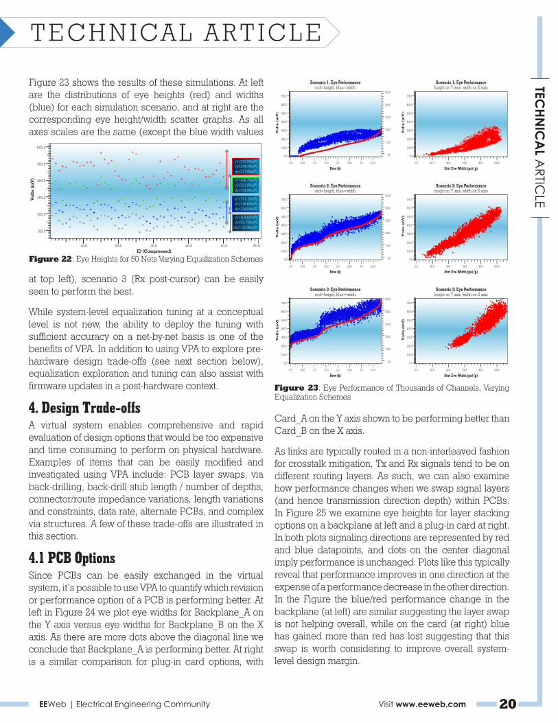
Figure 23 shows the results of these simulations. At left are the distributions of eye heights (red) and widths (blue) for each simulation scenario, and at right are the corresponding eye height/width scatter graphs. As all axes scales are the same (except the blue width values
Card_A on the Y axis shown to be performing better than Card_B on the X axis.
As links are typically routed in a non-interleaved fashion for crosstalk mitigation, Tx and Rx signals tend to be on different routing layers. As such, we can also examine how performance changes when we swap signal layers (and hence transmission direction depth) within PCBs. In Figure 25 we examine eye heights for layer stacking options on a backplane at left and a plug-in card at right. In both plots signaling directions are represented by red and blue datapoints, and dots on the center diagonal imply performance is unchanged. Plots like this typically reveal that performance improves in one direction at the expense of a performance decrease in the other direction. In the Figure the blue/red performance change in the backplane (at left) are similar suggesting the layer swap is not helping overall, while on the card (at right) blue has gained more than red has lost suggesting that this swap is worth considering to improve overall system-level design margin.
at top left), scenario 3 (Rx post-cursor) can be easily seen to perform the best.
While system-level equalization tuning at a conceptual level is not new, the ability to deploy the tuning with sufficient accuracy on a net-by-net basis is one of the benefits of VPA. In addition to using VPA to explore pre-hardware design trade-offs (see next section below), equalization exploration and tuning can also assist with firmware updates in a post-hardware context.
4. Design Trade-offs A virtual system enables comprehensive and rapid evaluation of design options that would be too expensive and time consuming to perform on physical hardware. Examples of items that can be easily modified and investigated using VPA include: PCB layer swaps, via back-drilling, back-drill stub length / number of depths, connector/route impedance variations, length variations and constraints, data rate, alternate PCBs, and complex via structures. A few of these trade-offs are illustrated in this section.
4.1 PCB Options Since PCBs can be easily exchanged in the virtual system, it’s possible to use VPA to quantify which revision or performance option of a PCB is performing better. At left in Figure 24 we plot eye widths for Backplane_A on the Y axis versus eye widths for Backplane_B on the X axis. As there are more dots above the diagonal line we conclude that Backplane_A is performing better. At right is a similar comparison for plug-in card options, with
Figure 22: Eye Heights for 50 Nets Varying Equalization Schemes
Figure 23: Eye Performance of Thousands of Channels, Varying Equalization Schemes
Vo
lts
(mV
)
ID (Compressed)
y1:(572.50mV)y2:(354.70mV)dy:(217.80mV)
y1:(426.70mV)y2:(231.80mV)dy:(194.90mV)
y1:(721.10mV)y2:(146.60mV)dy:(124.50mV)
y1:(204.60mV)y2:(93.730mV)
dy:(-110.90mV)
600.0
500.0
400.0
300.0
200.0
100.0
10.0 20.0 30.0 40.0 50.0 60.0
700.0
600.0
500.0
400.0
300.0
200.0
200.0
150.0
100.0
50.0
0.0
250.0
100.0
0.0
0.0 0.50 1.0 15.0 2.0 2.50 3.0 3.5.0
Row (k)
red=height, blue=widthScenario 1: Eye Performance
700.0
600.0
500.0
400.0
300.0
200.0
100.0
0.0
0.0 20.0 40.0 60.0 80.0 100.0
Stat Eve Width (ps) (p)
height on Y axis, width on X axisScenario 1: Eye Performance
Vo
lts (
mV
)
Vo
lts (
mV
)
700.0
600.0
500.0
400.0
300.0
200.0
100.0
0.0
0.0 20.0 40.0 60.0 80.0 100.0
Stat Eve Width (ps) (p)
height on Y axis, width on X axisScenario 2: Eye Performance
Vo
lts (
mV
)
700.0
600.0
500.0
400.0
300.0
200.0
100.0
0.0
0.0 20.0 40.0 60.0 80.0 100.0
Stat Eve Width (ps) (p)
height on Y axis, width on X axisScenario 3: Eye Performance
Vo
lts (
mV
)
700.0
600.0
500.0
400.0
300.0
200.0
200.0
150.0
100.0
50.0
0.0
250.0
100.0
0.0
0.0 0.50 1.0 15.0 2.0 2.50 3.0 3.5.0
Row (k)
red=height, blue=widthScenario 2: Eye Performance
Vo
lts (
mV
)
700.0
600.0
500.0
400.0
300.0
200.0
200.0
150.0
100.0
50.0
0.0
250.0
100.0
0.0
0.0 0.50 1.0 15.0 2.0 2.50 3.0 3.5.0
Row (k)
red=height, blue=widthScenario 3: Eye Performance
Vo
lts (
mV
)

EEWeb | Electrical Engineering Community Visit www.eeweb.com 21
TECHN
ICA
L ARTIC
LETECHNICAL ARTICLE
4.2 Via Back-drilling While back-drilling is common on thicker backplanes, another design option easily quantified by VPA is the performance benefit that comes from also back-drilling
measured at the reduced data rate on the Y axis. As such points above the line indicate an improvement in performance/margin, which is shown by the markers to be typically 37mV in height and 10 pS in width which translates to ~30% increase in design margin for an 8% reduction in data rate.
Figure 24: Eye Width vs. PCB Swapping, Backplane (left) and Plug-in Card (Right)
vias on thinner plug-in cards. Figure 26 plots eye height (left) and width (right) changes with (X axis) and without (Y axis) back-drilling on the plug-in card. As such, all points below the diagonal indicate an improvement due to back-drilling. The plots below reveal that all signals either stay the same or improve – some times as much as 50%. Note that while signals received by the card (in red) improve with back-drilling, improvement is even more dramatic for signals transmitted from the card (blue).
The plots reveal typically 20% improvement in margin on blue nets, yet more importantly improvement generally increases on signals with the least amount of margin.
4.3 Data Rate As architectural system-level throughput requirements change it’s common to assess how design margin changes with variation in data rate. Figure 27 reveals how eye height (left) and width (right) vary with an 8% decrease in data rate. Performance using the original data rate is on the X axis plotted against performance
4.4 Impedance Changes One way to alter discontinuities (and their related resonances) that limit performance is to change the impedance of nearby traces and connectors. Figure 28 plots how the eye height (red) and width (blue) changes in a channel limited by a discontinuity-induced resonance as we allow impedance variations in the dominant connectors and traces in the channel. Allowing four impedance options for traces on the backplane, both plug-in cards, and both connectors provides the 1,024 (210) permutations plotted on the X axis. From the plot we see that width tends to track height, and the eye opening can be improved up to 300%.
TDR plots of the original channel (lighter shades) and a channel with 300% eye improvement (in darker shades) are shown in Figure 29. Red is the direction of signal flow and blue shows the channel looking from Rx to Tx. Note that the impedance changes have not necessarily removed all the discontinuities, yet have certainly lengthened the distance between them.
Figure 25: Eye Height vs. PCB Layer Swapping, Backplane (left) and Plug-in Card (right)
Figure 26: Eye Height Variation When Back-drilling Plug-in Card
Figure 27: Eye Height and Width Improvements, 8% Data Rate Reduction
90.0
70.0
60.0
50.0
40.0
30.0
30.0 40.0 50.0 60.0 70.0 80.0
90.0
70.0
60.0
50.0
40.0
30.0
30.0 40.0 50.0 60.0 70.0 80.0
Tim
e (p
s)
Tim
e (p
s)
Stat Eve Width Single 52 (ps) (p) Stat Eve Width Single 52 (ps) (p)
140.0
120.0
100.0
80.0
60.0
40.0
20.0
140.0
160.0
120.0
100.0
80.0
60.0
40.0
30.0 40.0 60.0 80.0 100.0 120.0 140.0 40.0 60.0 80.0 100.0 120.0 140.0 160.0
Vo
lts
(mV
)
Vo
lts
(mV
)
Stat Eve Height Dual 44 (V) (m) Stat Eve Height Dual 44 Swap SC (V) (m)
160.0
140.0
120.0
100.0
80.0
60.0
40.0
40.0 60.0 80.0 100.0 120.0 150.0 160.0
Vo
lts
(mV
)
Stat Eve Height Dual 44 SC Backdrill (V) (m)
80.0
70.0
90.0
60.0
50.0
50.0 60.0 70.0 80.0 90.0
Tim
e (p
s)
Stat Eve Height Dual44 SC Backdrill (V) (m)
Stat Eve Height Dual 44 (V) (m) Stat Eve Height Dual 44 (bs) (p)
160.0
160.0
180.0
180.0
140.0
140.0
120.0
120.0
100.0
100.0
80.0
80.0
80.0
80.0
90.0
90.0
70.0
70.0
60.0
60.0
50.0
50.0
40.0
40.0
60.0
60.0
Vo
lts
(mV
)
Tim
e (p
s)
y1:(79.660ps)y2:(70.070ps)dy:-9.585ps
y1:(95.190mV)y2:(131.90mV)dy:36.710mV

EEWeb | Electrical Engineering Community Visit www.eeweb.com 22
TECHN
ICA
L ARTIC
LETECHNICAL ARTICLE
5. Summary In the coming decade, serial link analysis will be challenged not only by issues of frequency but also by issues of scale; trillions of bits will be processed
for their continued help in advancing channel design and improving the connector footprint. Additional thanks to Orlando Bell at GigaTest Labs for consistently delivering high quality measured data. Without the efforts of these and other people this work would not have been possible.
References [1] “Simulation Techniques for 6+ Gbps Serial Links” Telian, Camerlo, Kirk, DesignCon 2010 http://www.siguys.com/resources/2010_DesignCon_6GbpsSimTechniques_Paper.pdf
[2] “New Techniques for Designing and Analyzing Multi-GigaHertz Serial Links”, Telian, Wang, Maramis, Chung – DesignCon 2005, http://www.siguys.com/resources/2005_DesignCon_New_MGH_Techniques_ISP_CA_PCIe_SATA.pdf
[3] “Introducing Channel Analysis for PCB Systems”, 2004 Webinar, http://www.siguys.com/resources/2004_Webinar_Introducing_Channel_Analysis.pdf
[4] “New Serial Link Simulation Process, 6 Gbps SAS Case Study”, Telian, Larson, Ajmani, Dramstad, Hawes, DesignCon 2009 Paper Award, http://www.siguys.com/resources/2009_DesignCon_6Gbps_Simulation_Paper.pdf
[5] “Adapting Signal Integrity Tools and Techniques for 6 Gbps and Beyond”, Telian http://www.siguys.com/resources/2007_CDNLive_Adapting_SI_Tools_for_6Gbps+.pdf
[6] “Signals on Serial Links: Now you see ‘em, now you don’t.” DesignCon07 Article, http://www.siguys.com/resources/2007_Article_SignalsOnSerialLinks.pdf
[7] SAS Specification, SAS-2, Project T10/1760-D, Rev 16, 18 April 2009, see also USB 3.0 etc.
[8] For example, see LeCroy 10/12/11 Webinar “USB 3.0 – Electrical Compliance Testing” http://www.lecroy.com/support/techlib/webcasts.aspx?capid=106&mid=528&smid=663
[9] “Practical Analysis of Backplane Vias for 5 Gbps and Above”, E. Bogatin, L. Simonovich, C. Warwick and S. Gupta, paper 7-TA2, DesignCon2009, February 3, 2009.
[10] “A Simple Via Experiment”, Chong Ding, Divya
across thousands of channels. While traditional SI methodologies had succeeded in moving post-route analysis to more of a verification step [12], this paper has demonstrated how VPA greatly assists serial link development in areas of system-level equalization tuning and design trade-offs. Furthermore, due to the thousands of channel permutations analyzed, VPA has potential to identify performance limitations caused by unexpected and/or unavoidable discontinuities that may have been
overlooked by pre-route analysis. While challenges related to capacity, throughput, and accuracy must be solved to assemble an efficient virtual prototype system, this paper has demonstrated one approach taken and some of the benefits associated with overcoming these barriers.
Acknowledgements The authors wish to thank Shashi Aluru, Minh Nguyen and Radu Talkad at Ericsson and Todd Westerhoff at SiSoft for their support. Many thanks to Jim Mangin and Steve Barbas for their support of this effort, and to John Lehman, Jose Paniagua and Brian Kirk at Amphenol-TCS
Figure 28: Eye Height and Width Variation vs. Connector/Trace Impedance Permutations
Figure 29: TDR of Marginal Channel Improved by Impedance Changes
Vol
ts (m
V)
TIm
e (p
s)
Row (k)
20.0
1.00.20
40.0
60.0
80.0
100.0
0.60 0.800.400.0
80.0
90.0
70.0
60.0
50.0
40.0
Time (ns)
Oh
ms
70.0
0.0 1.0 2.0 3.0 4.0 5.0 6.0 7.0 8.0
80.0
90.0
100.0
110.0
120.0

EEWeb | Electrical Engineering Community Visit www.eeweb.com 23
TECHN
ICA
L ARTIC
LETECHNICAL ARTICLE
Gopinath, Steve Scearce, Mike Steinberger, Doug White, paper 5-TP2, DesignCon2009, February 3, 2009.
[11] “Practical Design of Differential Vias”, Bogatin, Simonovich, Cao, PCD&F, July 7, 2010 http://pcdandf.com/cms/component/content/ar ticle/171-current-issue/7302-eric-bogatin-bert-simonovich-and-yazi-cao
[12] “An Optimized Design Methodology for High-Speed Design” DesignCon 2008 http://www.siguys.com/resources/1998_DesignCon_Optimized_SI_Methodology.pdf
[13] “Demonstration of SerDes Modeling using the Algorithmic Modeling Interface (AMI) Standard”, Steinberger, Westerhoff, White, paper 7-TA3, DesignCon 2008
Sisoft Video Presentation and Corresponding Powerpoint: http://www.sisoft.com/elearning/webinars/simulating-large-systems-with-thousands-of-serial-links.html
Author’s BiographiesBarry Katz, President and CTO for SiSoft, founded SiSoft in 1995. As CTO, Barry is responsible for leading the definition and development of SiSoft’s products. He has devoted much of his efforts at SiSoft to delivering a comprehensive design methodology, software tools, and expert consulting to solve the problems faced by designers of leading edge high-speed systems. He was the founding chairman of the IBIS Quality committee. Barry received an MSEE degree from Carnegie Mellon and a BSEE degree from the University of Florida.
Michael Steinberger, Ph.D., Lead Architect for SiSoft, has over 30 years experience designing very high speed electronic circuits. Dr. Steinberger holds a Ph.D. from the University of Southern California and has been awarded 14 patents. He is currently responsible for the architecture of SiSoft’s Quantum Channel Designer tool for high speed serial channel analysis. Before joining SiSoft, Dr. Steinberger led a group at Cray, Inc. performing SerDes design, high speed channel analysis, PCB design and custom RAM design.
Dr. Walter Katz, Chief Scientist for SiSoft, is a pioneer in the development of constraint driven printed circuit board routers. He developed SciCards, the first
commercially successful auto-router. Dr. Katz founded Layout Concepts and sold routers through Cadence, Zuken, Daisix, Intergraph and Accel. More than 20,000 copies of his tools have been used worldwide. Dr. Katz developed the first signal integrity tools for a 17 MHz 32-bit minicomputer in the seventies. In 1991, IBM used his software to design a 1 GHz computer. Dr. Katz holds a PhD from the University of Rochester, a BS from Polytechnic Institute of Brooklyn and has been awarded 5 U.S. Patents.
Sergio Camerlo is an Engineering Director with Ericsson Silicon Valley (ESV), which he joined through the Redback Networks acquisition. His responsibilities include the Chassis/Backplane infrastructure design, PCB Layout Design, System and Board Power Design, Signal and Power Integrity. He also serves on the company Patent Committee and is a member of the ESV Systems and Technologies HW Technical Council. In his previous assignment, Sergio was VP, Systems Engineering at MetaRAM, a local startup, where he dealt with die stacking and 3D integration of memory. Before, Sergio spent close to a decade at Cisco Systems, where he served in different management capacities. Sergio has been awarded fourteen U.S. Patents on signal and power distribution, interconnects and packaging.
Donald Telian is an independent Signal Integrity Consultant. Building on over 25 years of SI experience at Intel, Cadence, HP, and others, his recent focus has been on helping customers correctly implement today’s Multi-Gigabit serial links. He has published numerous works on this and other topics that are available at his website siguys.com. Donald is widely known as the SI designer of the PCI bus and the originator of IBIS modeling and has taught SI techniques to thousands of engineers in more than 15 countries. ■

EEWeb | Electrical Engineering Community Visit www.eeweb.com 24
FEATURED
PROD
UCTS
FEATURED PRODUCTS
High Current PMIC Without ChargerThe AS3713 is a compact System PMU with back light driver. The device offers advanced power management functions. All necessary ICs and peripherals in a battery powered mobile device are supplied by the AS3713. It features 3 DCDC buck converters as well as 8 low noise LDOs. The different regulated supply voltages are programmable via the serial control interface. 4MHz operation with 1uH coils are reducing cost and PCB space. For more information, please click here.
42V, 2.5A, 5A, 2MHz DC/DC ConvertersLinear Technology Corporation announced the LT3975, a 42V step-down switching regulator that can deliver 2.5A of continuous output current and requires only 2.7µA of quiescent current. Similarly, the LT3976 can operate from a 40V input, delivers up to 5A of output current and requires only 3.3µA of quiescent current. Both devices offer a 4.2V to a nominal 40V input voltage range, making them ideal for automotive and industrial applications. The combination of their 16-lead thermally enhanced MSOP package and high switching frequency keeps external inductors and capacitors small, providing a compact, thermally efficient footprint. For more information, please click here.
Ultrasound Receiver I/Q DemodulatorAnalog Devices, Inc. introduced the industry’s first octal (eight-channel) ultrasound receiver with on-chip digital I/Q demodulation and decimation filtering. Because of the embedded demodulation and decimation feature, ADI’s AD9670 is the first ultrasound receiver able to condition eight channels of data from RF to a baseband frequency, reducing the processing load on the system FPGA by at least 50 percent compared to other receivers. The new octal receiver is the latest addition to Analog Devices’ award winning ultrasound receiver portfolio and is designed for mid- to high-end portable and cart-based ultrasound systems. For more information, please click here.
Diode Protection for Transient VoltagesLinear Technology Corporation introduces the LTC4364, a surge stopper with ideal diode, providing compact and low-loss protection for 4V to 80V electronics in automotive, avionics and industrial systems. The surge stopper shields downstream electronics from input overvoltages and overcurrent, enabling continuous operation through transient surges. Overcurrent limiting protects the system and supply from short-circuits at the load. Unique to the LTC4364 is ideal diode control, which replaces a Schottky diode in the power path with a low loss N-channel MOSFET. The ideal diode, along with a robust front-end, protects the load from a reversed input down to -40V and maintains the output voltage during an input brownout. For more information, please click here.
LT3975
93975p
BLOCK DIAGRAM
+–
+–
+–
+–
OSCILLATOR200kHz TO 2MHz
Burst ModeDETECT
VC CLAMPVC
SLOPE COMP
R
VINVIN
EN BOOST
0.5V
SW
SHDN
SWITCHLATCH
SS1.8μA
VOUT
C2
C3
C4OPT
L1
D1
OUT
RT
R2
GND
ERROR AMP
R1
FB
RT
C1
PG
1.097V
1.02V
SQ
3975 BD
INTERNAL 1.197V REF
SYNC
+– SHDN +
C5
+–

Electric
al Engine
ering C
ommunity
EEWeb
ARTICLES
JOBS
COMMUNITY
DEVELOPMENT TOOLS
Dave BaarmanDirector Of
Advanced Technologies
Making WirelessTruly Wireless:
Need For UniversalWireless Power
Solution
"Sed ut perspiciatis unde omnis
iste natus error sit voluptatem
accusantium doloremque
laudantium, totam rem aperiam,
eaque ipsa quae ab illo inventore
veritatis et quasi architecto beatae vitae
dicta sunt explicabo. Nemo enim ipsam
voluptatem quia voluptas sit aspernatur aut odit
aut fugit, sed quia consequuntur magni dolores eos
qui ratione voluptatem sequi nesciunt. Neque porro
quisquam est, qui dolorem ipsum quia dolor sit amet, consectetur,
adipisci velit, sed quia non numquam eius modi tempora incidunt ut
labore et dolore magnam aliquam quaerat voluptatem. Ut enim ad
minima veniam, quis nostrum exercitationem ullam corporis suscipit
laboriosam, nisi ut aliquid ex ea commodi consequatur? Quis autem
vel eum iure reprehenderit qui in ea voluptate velit esse quam nihil
www.eeweb.com
JOINTODAY

EEWeb | Electrical Engineering Community Visit www.eeweb.com 26
Thermocouples are far and away the most widely used type of temperature sensor because they are both rugged and relatively inexpensive. They operate based on the thermoelectric or Seebeck effect (named after physicist Thomas Seebeck). When two wires made up of dissimilar metals are joined together, a voltage is generated. The level of generated voltage is a function of temperature. As temperature changes, the voltage changes, so the thermocouple’s voltage output equates to a temperature reading.
The linearity of a thermocouple’s output varies depending on thermocouple type and temperature range. Although thermocouples can cover a very wide range of temperatures (some as high as 2300°C), they produce
very small output voltages, so the instrumentation used with them must provide sufficient resolution to discern small voltage changes.
Several sources of temperature measurement error are specific to thermocouples:
• The CJC (Cold Junction Compensation) is not configured or compensated—Thermocouples measure the difference in temperature between the hot junction (used for the actual measurement) and the cold or reference junction (at the instrument). If the temperature of the cold junction is not known or not compensated for (by means of cold junction compensation), the temperature readings will be inaccurate.
• Use of copper wire from the
thermocouple connection to the measurement instrument—Connections between the thermocouple and the instrument should be made with the same kind of wire used for the thermocouple. In theory, one could use copper wire, but that would require controlling the temperature of all the wire, which is generally impractical.
• The voltage measurement instrumentation is not sensitive or accurate enough for thermocouple measurements—The output of a thermocouple is just microvolts, so be sure to choose an instrument with sufficient resolution to measure microvolts accurately. Fortunately, many modern digital multimeters (DMMs) offer built-in capabilities that make them particularly appropriate for thermocouple temperature measurements.
Robert GreenKeithley Senior Market Development Manager
ThermocouplesPART II
Optimizing Your NextTemperature MeasurementConfiguration

EEWeb | Electrical Engineering Community Visit www.eeweb.com 27
TECHN
ICA
L ARTIC
LETECHNICAL ARTICLE
For example, Keithley’s Model 3706A System Switch/Multimeter supports J, K, N, T, E, R, S, and B thermocouple types. Depending on which type of thermocouple you choose, this instrument allows you to measure temperatures from -200°C to 1820°C at resolution levels from 0.001°C (with type J) to 0.1°C (with type B).
When a thermocouple is connected directly to the input of a DMM, at least one of those connections will be a junction made up of two dissimilar metals, introducing a thermoelectrical voltage that will be algebraically added to the thermocouple voltage, producing an erroneous temperature measurement. To cancel the effects of this unwanted thermoelectrical voltage where dissimilar wire connections must be made, the thermocouple circuit requires a reference junction that is held at a stable, known temperature.
For example, as long as the temperature of this reference (cold) junction is known, the DMM can factor in the reference temperature
to calculate the actual temperature reading at the thermocouple. Although the standard reference temperature used as the fundamental reference for NIST’s voltage-to-temperature conversion tables is the ice point (0°C), other known temperatures can be used. For example, some DMMs can acquire the cold junction temperature by measuring the cold junction using a thermistor or four-wire RTD, or the user can enter the known temperature value.
The most accurate thermocouple measurements are achieved by using a simulated reference junction using an ice point reference (Figure 1). The copper wire to thermocouple wire connections are immersed (but electrically isolated) in the ice bath, and the user enters the 0°C simulated reference temperature into the instrument.
Long lengths of thermocouple wire can have a significant amount of capacitance, which is seen at the input of the DMM. If an intermittent open occurs in the thermocouple circuit, this capacitance can
produce an erroneous on-scale reading. To prevent these errors, look for an instrument that provides an open thermocouple detection circuit.
About the AuthorRobert Green is a Senior Market Development Manager at Keithley Instruments focusing on low level measurement applications. During his 20-year career at Keithley, Mr. Green has been involved in the definition and introduction of a wide range of products including picoammeters, electrometers, digital multimeters, and temperature measurement products. He received a B.S. in Electrical Engineering from Cornell University and an M. S. in Electrical Engineering from Washington University, St. Louis, Missouri. ■
Figure 1: A simulated reference junction using an ice point reference.
+
T
Ice bath
–
Copper wire to thermocouplewire connection (one of two)Analog Backplane Connection
Thermocouple
Copper wiresINPUT HI
INPUT LOW
19
158
Pin 1
Pin 2or
Pin 9

Ultra-Low Lux, Low Power, Integrated Digital Ambient Light Sensor with Interrupt FunctionISL29033The ISL29033 is an integrated ambient and infrared light to digital converter with I2C (SMBus Compatible) interface. Its advanced, self-calibrated photodiode array emulates human eye response with excellent IR rejection. The on-chip 16-bit ADC is capable of rejecting 50Hz and 60Hz flicker caused by artificial light sources. The lux range select feature allows users to program the lux range for optimized counts/lux. Power consumption can be reduced to less than 0.3µA when powered down.
The ISL29033 supports a software and hardware interrupt that remains asserted until the host clears it through the I2C interface. The function of ADC conversion continues without stopping after interrupt is asserted.
Designed to operate on supplies from 2.25V to 3.63V with an I2C supply from 1.7V to 3.63V, the ISL29033 is specified for operation over the -40°C to +85°C ambient temperature range.
Related Literature• See AN1422 “Light Sensor Applications”
Features• Ambient Light Sensing
• Simple Output Code Directly Proportional to Lux
• Variable Conversion Resolution Up to 16 Bits
• Adjustable Sensitivity Up to 520 Counts Per Lux
• Measurement Range: 0.0019 to 8,000Lux with Four Selectable Ranges
• Program Interrupt Feature
• Light Sensor Close to Human Eye Response
- Excellent Light Sensor IR and UV Rejection
• 75μA Max Operating Current- 0.3μA Max Shutdown Current
• 6 Ld 2.0mmx2.1mmx0.7mm ODFN Package
Applications• Display and Keypad Dimming Adjustment for:
- Mobile Devices: Smart Phone, PDA, GPS- Computing Devices: Notebook PC, Webpad- Consumer Devices: LCD-TV, Digital Picture Frame, Digital
Camera• Industrial and Medical Light Sensing
VDD
REXT GND
SDASCL
COMMANDREGISTER
INTEGRATIONADC
DATAREGISTER
PHOTODIODE
LIGHT
3 2
56
1
fOSC
IREF
4
INT
PROCESS
ARRAY
DATA
I2C/SMBus
INTERRUPT REGISTER
FIGURE 1. BLOCK DIAGRAM
September 30, 2011FN7656.1
Intersil (and design) is a registered trademark of Intersil Americas Inc. Copyright Intersil Americas Inc.2011All Rights Reserved. All other trademarks mentioned are the property of their respective owners.
Get the Datasheet and Order Samples
http://www.intersil.com

EEWeb | Electrical Engineering Community Visit www.eeweb.com 29
TECHN
ICA
L ARTIC
LETECHNICAL ARTICLE Jonpaul Jandu
Intersil BusinessDevelopment Manager
FisheyeIC Lens
CorrectionMade Simple
Fisheye images, spanning a field of view of up to 180 degrees, can offer fascinating and exotic qualities. They offer a density of visual information that is otherwise inaccessible to the naked eye or by the use of regular ‘pinhole’ type cameras, even when fitted with a wide-angle lens. The extreme barrel-shaped warping of the image, as if looking at a globe, is often quite acceptable – even valued – as a visually ‘interesting’ picture.
However, a different situation emerges if one considers the possible commercial or industrial applications for a fisheye image. Such applications usually depend on a regular, equidistant-matrix, rectilinear picture format. Extreme fisheye warping results in radial dislocations of the picture elements in a non-linear pattern. The pixels appear spatially shifted to the edges, away from the image’s centre of distortion – which usually, but not necessarily, is also its focal point and visual center. One must add to that the effects of uneven luminance and colour saturation caused by the enormous directional light and shadow variations across the field of view, plus chromatic aberrations and tangential pixel dislocations introduced by the limited optical quality of the lens. Unfortunately, even though perhaps appealing at first glance, the raw data coming from a fisheye lens is not suited to computer vision applications, or the detection and recognition of objects and their movements across the picture plane. Even for visual observation
in surveillance systems the extremely distorted view is almost unusable.
Basically, to be useful, fisheye images need a heavy dose of optical correction before they are suitable to use as an input for real-world applications.
The ‘fix’ is a carefully balanced image correction procedure that transforms the distorted and shifted image elements back to their ‘natural’ rectilinear matrix, if possible in real time to generate a live video stream. Traditionally, this requires photogammetric calibration or, simpler but less flexible, pragmatic correction and adjustment of the picture content by visually matching its geometry with known objects and scenes. There are algorithms available for this, based on complex polynomic equations employing perspective or gradient-of-resolution modeling, amongst others.
This procedure usually involves excessive post-processing – which prohibits high-end real-time applications of digital video streams as required in many live image analysis tasks. Additionally, most of these algorithms have been established and optimized to serve proprietary formats and specific applications.
This set of conditions was the starting point for the development of Intersil’s TW2871, which began in Tokyo in 2009. The basic idea was to provide camera
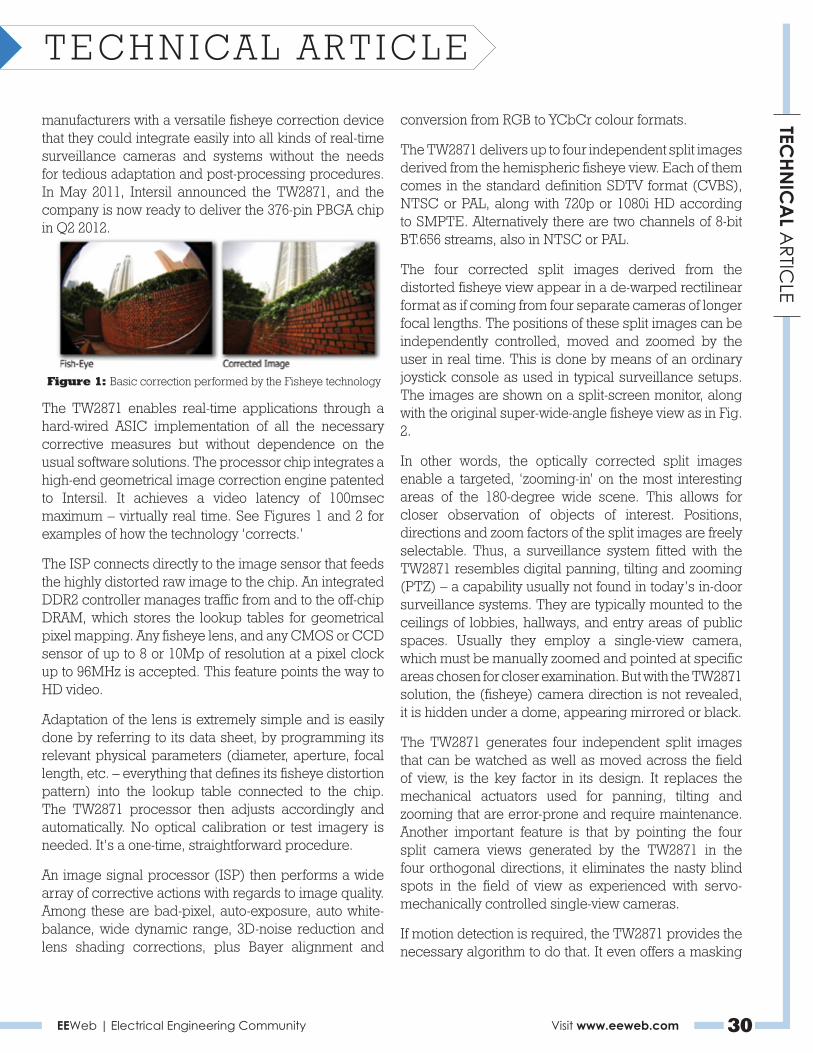
EEWeb | Electrical Engineering Community Visit www.eeweb.com 30
TECHN
ICA
L ARTIC
LETECHNICAL ARTICLE
Figure 1: Basic correction performed by the Fisheye technology
manufacturers with a versatile fisheye correction device that they could integrate easily into all kinds of real-time surveillance cameras and systems without the needs for tedious adaptation and post-processing procedures. In May 2011, Intersil announced the TW2871, and the company is now ready to deliver the 376-pin PBGA chip in Q2 2012.
conversion from RGB to YCbCr colour formats.
The TW2871 delivers up to four independent split images derived from the hemispheric fisheye view. Each of them comes in the standard definition SDTV format (CVBS), NTSC or PAL, along with 720p or 1080i HD according to SMPTE. Alternatively there are two channels of 8-bit BT.656 streams, also in NTSC or PAL.
The four corrected split images derived from the distorted fisheye view appear in a de-warped rectilinear format as if coming from four separate cameras of longer focal lengths. The positions of these split images can be independently controlled, moved and zoomed by the user in real time. This is done by means of an ordinary joystick console as used in typical surveillance setups. The images are shown on a split-screen monitor, along with the original super-wide-angle fisheye view as in Fig. 2.
In other words, the optically corrected split images enable a targeted, ‘zooming-in’ on the most interesting areas of the 180-degree wide scene. This allows for closer observation of objects of interest. Positions, directions and zoom factors of the split images are freely selectable. Thus, a surveillance system fitted with the TW2871 resembles digital panning, tilting and zooming (PTZ) – a capability usually not found in today’s in-door surveillance systems. They are typically mounted to the ceilings of lobbies, hallways, and entry areas of public spaces. Usually they employ a single-view camera, which must be manually zoomed and pointed at specific areas chosen for closer examination. But with the TW2871 solution, the (fisheye) camera direction is not revealed, it is hidden under a dome, appearing mirrored or black.
The TW2871 generates four independent split images that can be watched as well as moved across the field of view, is the key factor in its design. It replaces the mechanical actuators used for panning, tilting and zooming that are error-prone and require maintenance. Another important feature is that by pointing the four split camera views generated by the TW2871 in the four orthogonal directions, it eliminates the nasty blind spots in the field of view as experienced with servo-mechanically controlled single-view cameras.
If motion detection is required, the TW2871 provides the necessary algorithm to do that. It even offers a masking
The TW2871 enables real-time applications through a hard-wired ASIC implementation of all the necessary corrective measures but without dependence on the usual software solutions. The processor chip integrates a high-end geometrical image correction engine patented to Intersil. It achieves a video latency of 100msec maximum – virtually real time. See Figures 1 and 2 for examples of how the technology ‘corrects.’
The ISP connects directly to the image sensor that feeds the highly distorted raw image to the chip. An integrated DDR2 controller manages traffic from and to the off-chip DRAM, which stores the lookup tables for geometrical pixel mapping. Any fisheye lens, and any CMOS or CCD sensor of up to 8 or 10Mp of resolution at a pixel clock up to 96MHz is accepted. This feature points the way to HD video.
Adaptation of the lens is extremely simple and is easily done by referring to its data sheet, by programming its relevant physical parameters (diameter, aperture, focal length, etc. – everything that defines its fisheye distortion pattern) into the lookup table connected to the chip. The TW2871 processor then adjusts accordingly and automatically. No optical calibration or test imagery is needed. It’s a one-time, straightforward procedure.
An image signal processor (ISP) then performs a wide array of corrective actions with regards to image quality. Among these are bad-pixel, auto-exposure, auto white-balance, wide dynamic range, 3D-noise reduction and lens shading corrections, plus Bayer alignment and

EEWeb | Electrical Engineering Community Visit www.eeweb.com 31
TECHN
ICA
L ARTIC
LETECHNICAL ARTICLE
function to avoid false alarms. Masking a certain area of a split image by simply pointing and clicking from the console excludes visual objects that show regular unsuspicious motion patterns from the scrutiny of the motion detector.
necessary algorithm to do that. It even offers a masking function to avoid false alarms. Masking a certain area of a split image by simply pointing and clicking from the console excludes visual objects that show regular unsuspicious motion patterns from the scrutiny of the motion detector.
The four digital images delivered by the TW 2871 are de-warped and optically corrected up to XGA resolution, which is better than standard-definition (SD) TV quality. The final resolution is of course within the bounds of a digital zoom, which cannot go beyond the native pixel count of the original fisheye image. This limits surveillance applications mostly to indoor situations, at an object distance below 150 meters. However, future versions of the chip envisage HD resolution (1080i or 720p). In any case, optical zooming setups can now be relegated to outdoor surveillance situations that need to cover very large distances.
Most important to the designer of surveillance systems is that the new chip provides a convenient way of implementing fisheye correction without time-consuming software-driven procedures such as panorama stitching. In most cases these are too complex and too cost-intensive to be done in real time. The TW2871 hard-wired implementation enables image processing and correction to be done within the camera (but outside of the lens!). The camera can be installed in the immediate vicinity of the scene to be surveyed. But, as a stand-
The four digital images delivered by the TW 2871 are de-warped and optically corrected up to XGA resolution, which is better than standard-definition (SD) TV quality. The final resolution is of course within the bounds of a digital zoom, which cannot go beyond the native pixel count of the original fisheye image. This limits surveillance applications mostly to indoor situations, at an object distance below 150 meters. However, future versions of the chip envisage HD resolution (1080i or 720p). In any case, optical zooming setups can now be relegated to outdoor surveillance situations that need to cover very large distances.
The TW2871 generates four independent split images that can be watched as well as moved across the field of view, is the key factor in its design. It replaces the mechanical actuators used for panning, tilting and zooming that are error-prone and require maintenance. Another important feature is that by pointing the four split camera views generated by the TW2871 in the four orthogonal directions, it eliminates the nasty blind spots in the field of view as experienced with servo-mechanically controlled single-view cameras.
If motion detection is required, the TW2871 provides the
Figure 2: Example of corrected split image views plus original
fisheye view
Figure 3: TW2871 Evaluation Board for camera development purposes

EEWeb | Electrical Engineering Community Visit www.eeweb.com 32
TECHN
ICA
L ARTIC
LETECHNICAL ARTICLE
alone solution, it doesn’t need a ‘big-box’ PC or other processing unit nearby, and no transporting of Gigabytes of raw image data over high-speed links.
Besides surveillance systems, Intersil envisages future automotive driver-assistance applications. The concept calls for one fisheye camera mounted in the front, and another one in the back of a car. This would yield all the necessary views; front, left and right hand sides, and back, all corrected in the cameras. For this application, the current TW2871 layout may be an overkill; a ‘superset’ of all the required driver assistance features. Car drivers need no PTZ, just reliable fixed views to all sides of the vehicle. More relevant in the automotive context is that the system, besides being very low-cost, should last up to 20 years.
There definitely are many potential applications for the chip. Another one is video conferencing of larger groups, where the entire scene needs to be viewed, incorporating fast and flexible zooming in on participants as needed. There are also military applications in explosives seeking
robots that need to view their entire surroundings. There are medical applications where it is desirable to provide multiple imagery for endoscopy procedures. There is also a home security system made simple; a single-lens camera supplying various angles and levels of digital output that comply with popular digital consumer video formats and IP transfer.
About the AuthorJonpaul Jandu is business development manager at Intersil Corporation. He was previously employed by Techwell Corp. prior to its acquisition by Intersil. He holds a BS in Finance from Santa Clara University. ■
BeStar®
ACOUSTICS & SENSORS
Teamwork • Technology • Invention • Listen • Hear
PRODUCTSSpeakers
Buzzers
Piezo Elements
Back-up Alarms
Horns
Sirens/Bells
Beacons
Microphones
Sensors
INDUSTRIESAutomotive
Durables
Medical
Industrial
Mobile
Fire / Safety
Security
Consumer
Leisure
QS9000 • TS/ ISO16949 • ISO14001 • ISO13485 • ISO9001
bestartech.com | [email protected] | 520.439.9204
Preferred acoustic componentsupplier to OEMs worldwide

EEWeb | Electrical Engineering Community Visit www.eeweb.com 33
RETURN TO
ZERORETURN TO ZERO
EEWebElectrical Engineering Community
Join Todaywww.eeweb.com/register