


EEWeb Pulse - Issue 76
36
1 Visit www.eeweb.com INTERVIEW
description
Interview with Samta Bansal - Senior Manager, Product Marketing at Cadence; Taming the Challenges of 20nm Custom/Analog Design; MCU Wars 2.2 - Supporting MCUs in an RTOS; Distribution Systems - Part 3; RTZ - Return to Zero Comic
Transcript of EEWeb Pulse - Issue 76

1Visit www.eeweb.com
EEWeb PULSE INTERVIEW
EEWebIssue 76
December 11, 2012
Electrical Engineering Community eeweb.com
Challenges of20nm AnalogDesign
TECHNICAL ARTICLE
MCU Wars 2.2 -Supporting MCUsin an RTOS
SPECIAL FEATURE
Senior Manager,Product MarketingCadence
SamtaBansal

ExpertsExchanging IdeasEvery Day.VISIT DIGIKEY.COM/TECHXCHANGE TODAY!
Digi-Key is an authorized distributor for all supplier partners. New products added daily. © 2012 Digi-Key Corporation, 701 Brooks Ave. South, Thief River Falls, MN 56701, USA
EEWeb PULSE TABLE OF CONTENTS
3Visit www.eeweb.com
Samta Bansal CADENCE
Interview with Samta Bansal - Senior Manager, Product Marketing
The challenges that custom and analog designers face from the manufacturing complexity in 20 nm IC design.
RTZ - Return to Zero Comic
Featured Products
BY SAMTA BANSAL WITH CADENCE
4
13
14
26
Taming the Challenges of 20nm Custom
MCU Wars 2.2: Supporting MCUs in
36
Two experts in RTOS sit down to discuss the advantages of supporting MCUs in a real-time operating system as well as the risks of writing your own system.
an RTOS
Analog Design
Distribution Systems - Part 3BY NICHOLAS ABI-SAMRA WITH QUANTA TECHNOLOGYWhy Distribution Automation (DA) is considered in developing the Smart Grid as it transforms the distribution network towards more automation.
30

4
EEWeb PULSE INTERVIEW
EEWeb | Electrical Engineering Community
BansalCadence
5Visit www.eeweb.com
EEWeb PULSE INTERVIEW
BansalCadence
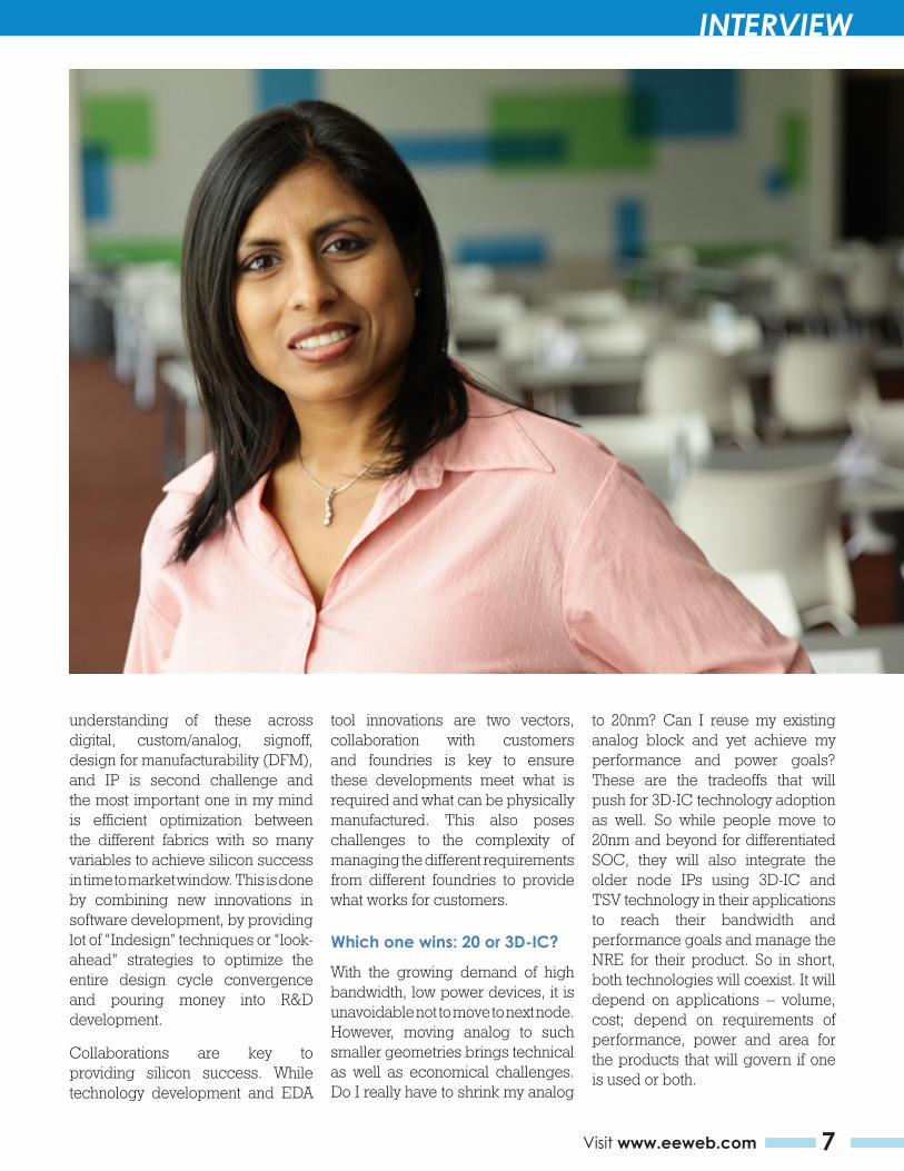
Cadence Design Systems is a leading global EDA com-pany that specializes in custom ICs and electronic sys-tems. We spoke with the Senior Manager of Product Mar-keting, Samta Bansal, about the challenges of silicon realization, the advantages of moving to 20nm ICs and the overall benefits of the 20nm process technology.

6
EEWeb PULSE INTERVIEW
EEWeb | Electrical Engineering Community
Can you tell us about your work experience/history before you became Senior Manager, Product Marketing, Silicon Realization at Cadence?
After my masters in Physics and Bachelors in EEE, I joined as application engineer focusing on DFT and ATPG solutions and soon expanded into front end synthesis. After spending few years as core technical, I completed my MBA and jumped into marketing to contribute on the business and strategy of the products – always what I had wanted to do.
It was becoming obvious that power and performance will become more of an issue as we go along the Moore curve and advance node shrink will go only so far. Achieving design closure required more integrated approach to the design methodology than “over the wall” methods that existed at that time. So I started focusing on Hierarchical methodologies, System exploration techniques, links to front end and back end, understanding packaging and how it impacts the design and design closure and that expanded my horizon to deeper understanding of not only the gaps that existed between EDA tools at that time but also the trends that are going to impact how we do design and how we provide software in EDA tools to help out. With this broader outlook, I worked on numerous efforts like Giga Gates, 3D-IC, Advanced node among others across product groups to help bring synergies among the tools at Cadence. This was core to Silicon realization group – which stands for ensuring that we can deliver for the silicon for our designers. So my work at Cadence allows me to look at the complete picture and help identify efficiencies and deficiencies within our offerings
and provide for more rounded approach to issues like 20nm, 3D-IC to our customers.
What are some general challenges for silicon realization?
Challenges revolve around “What will it take to achieve silicon success at 20nm and below.”
This includes combination of
a) Technology innovation: New technologies to provide for consumer demands of performance, power and area
b) EDA tools and techniques: In addition to adopting the new technologies EDA tools also need to provide improved efficiency and certainty for silicon success.
c) Collaborations with customers and foundries are becoming more and more important to deliver against that challenge.
Let me talk about these one at a time:
Technology scaling is not over. However it’s going to be a lot harder to move the technology forward and achieve the performance, power, and density requirements that will
make the technology interesting for customers. Innovations in strain engineering and high-k metal gates (HKMG) have kept things going so far however we are coming to the end of the planar era. Technology development such as 3D devices like FinFETs or tri-gates, 3D-IC TSVs is required now and probably exploring things like silicon nanowires, carbon nanotubes, and the integration of photonics onto the wafer have to start as well. So continued technology innovation is critical to Silicon success and a challenge for Silicon realization.
EDA Tools and Techniques: Let us take a small example of EDA tool challenges: Advanced process nodes generate hundreds of design rules - But can people still generate good designs? If we make spacing larger or voltage higher, we solve some problems, but then we don’t get the density, frequency and power advantages of process developments. So the question is whether the designer can design optimally enough with the resources they have and how can EDA tools help?
So understanding the additions and constraints the new technologies, new nodes bring is one, seamless
“My work at Cadence allows me to look at the complete picture and help identify efficiencies and deficiencies within our offerings and provide for
more rounded approach to issues like 20nm, 3D-IC to our customers.”
7Visit www.eeweb.com
EEWeb PULSE INTERVIEW
understanding of these across digital, custom/analog, signoff, design for manufacturability (DFM), and IP is second challenge and the most important one in my mind is efficient optimization between the different fabrics with so many variables to achieve silicon success in time to market window. This is done by combining new innovations in software development, by providing lot of “Indesign” techniques or “look-ahead” strategies to optimize the entire design cycle convergence and pouring money into R&D development.
Collaborations are key to providing silicon success. While technology development and EDA
tool innovations are two vectors, collaboration with customers and foundries is key to ensure these developments meet what is required and what can be physically manufactured. This also poses challenges to the complexity of managing the different requirements from different foundries to provide what works for customers.
Which one wins: 20 or 3D-IC?
With the growing demand of high bandwidth, low power devices, it is unavoidable not to move to next node. However, moving analog to such smaller geometries brings technical as well as economical challenges. Do I really have to shrink my analog
to 20nm? Can I reuse my existing analog block and yet achieve my performance and power goals? These are the tradeoffs that will push for 3D-IC technology adoption as well. So while people move to 20nm and beyond for differentiated SOC, they will also integrate the older node IPs using 3D-IC and TSV technology in their applications to reach their bandwidth and performance goals and manage the NRE for their product. So in short, both technologies will coexist. It will depend on applications – volume, cost; depend on requirements of performance, power and area for the products that will govern if one is used or both.

8
EEWeb PULSE INTERVIEW
EEWeb | Electrical Engineering Community
What would it take to adopt 20nm and 3DIC?Adopting advanced technologies will depend upon solving the technical challenges both from design and manufacturing ends, EDA tool readiness, wider collaborations in the ecosystem and last but not the least how cost effective the technology in the end happens to be.
a) Architecting a scalable and repeatable model around technical challenges: While the technology innovations are taking place with double patterning, FinFETs, low power, and through-silicon vias (TSVs) they all have their challenges. For instance, double patterning requires a decomposition method and a router that can support double patterning rules. FinFETs require SPICE modeling. TSVs raise thermal issues and bring challenges on bonding, debonding and probing technologies among several others. Entire DFT and ATPG methodology have to be architected to test the dies in the 3D stack. Can we move from “restrictive” advanced node design rules to “prescriptive” design rules? So these and many many others have to be resolved before mass adoption of a technology can take place. We have and always will have “early adaptors” for the technologies but for mass adoption scalability and repeatability is important.
b) EDA tool readiness is important. While these technologies are evolving, keeping EDA tools in pace with the innovations is very demanding but necessary. This is where collaborations with partners, experiences on test chips with “early adaptors” are critical towards architecting a repeatable and dependable solution for mass adoption. For 20nm we have so far more than 25 design already
done with critical partners in the ecosystem, and about 8 testchips and 1 production chips in 3D-IC with several inflight.
c) Wider collaboration will be must. With the economical pressures each industry is in today, an IDM-like model, where you have the benefits of a very close collaboration between design and manufacturing without having the economic issues of owning an $8 billion fab will become a must at 20nm and beyond. For 3D-IC it will extend even further where entire semiconductor business model will have to evolve and agreed upon to ensure ownership, accountability and reliability of the final product.
d) Last but not the least, Overall cost of the technology has to make sense. Everyone is in this industry to make money. If a technology can’t help make money it dies. So helping reduce cost for any new technology is the key to its wider adoption. It holds true for 20nm, FinFETs, SOI process and for TSVs as well.
What are the cost implications of 20nm and 3DIC – one or both?
As with any new technologies, there are risks, uncertainties and inefficiencies in the process of design and manufacturing and the yields related to those. Same holds true for advanced node like 20nm with Double-patterning, FinFETs and TSVs.
Today, 20nm brings in requirements of Dual mask for example. That is one added step in the manufacturing cost. 20nm requires extra design steps in the process – coloring etc. That is another cost added at design stage in terms of how much time it takes to do designing at 20nm. 20nm designs are complex enough that more people resources are required to address the design issues which adds to the cost of human power required to do 20nm and many others. So the costs are surrounding manufacturing, people, design, EDA tools etc. Everyone wants a premium for their early
“While today it may appear costly to adopt these advanced node
technologies, in terms of overall benefit and tradeoff with the
performance, power gains and sometimes yield gains as well that
these technologies might bring, more than often, the cost offsets itself.”
9Visit www.eeweb.com
EEWeb PULSE INTERVIEW development work and that is what makes any new technology in the beginning expensive for everyone.
3D-IC adds more complexity to this cost equation with potential of several fabs, several EDA vendors, Several IPs, testing complexity of the stack among several others.
However given time to any new technology, the manufacturing matures, designs and design challenges are well understood, EDA tools become efficient which in turn leads to lower costs to enable wider adoption of technology.
While today it may appear costly to adopt these advanced node technologies, in terms of overall benefit and tradeoff with the performance, power gains and sometimes yield gains as well that these technologies might bring, more than often, the cost offsets itself.
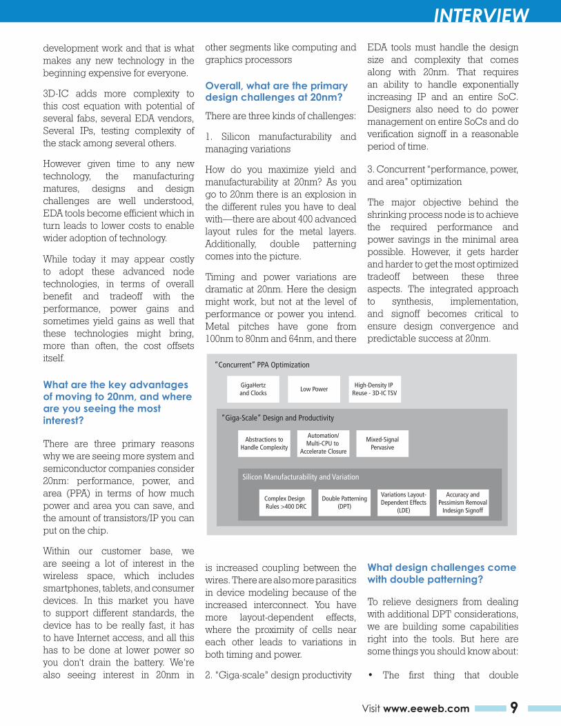
What are the key advantages of moving to 20nm, and where are you seeing the most interest?
There are three primary reasons why we are seeing more system and semiconductor companies consider 20nm: performance, power, and area (PPA) in terms of how much power and area you can save, and the amount of transistors/IP you can put on the chip.
Within our customer base, we are seeing a lot of interest in the wireless space, which includes smartphones, tablets, and consumer devices. In this market you have to support different standards, the device has to be really fast, it has to have Internet access, and all this has to be done at lower power so you don’t drain the battery. We’re also seeing interest in 20nm in
other segments like computing and graphics processors
Overall, what are the primary design challenges at 20nm?
There are three kinds of challenges:
1. Silicon manufacturability and managing variations
How do you maximize yield and manufacturability at 20nm? As you go to 20nm there is an explosion in the different rules you have to deal with—there are about 400 advanced layout rules for the metal layers. Additionally, double patterning comes into the picture.
Timing and power variations are dramatic at 20nm. Here the design might work, but not at the level of performance or power you intend. Metal pitches have gone from 100nm to 80nm and 64nm, and there
EDA tools must handle the design size and complexity that comes along with 20nm. That requires an ability to handle exponentially increasing IP and an entire SoC. Designers also need to do power management on entire SoCs and do verification signoff in a reasonable period of time.
3. Concurrent “performance, power, and area” optimization
The major objective behind the shrinking process node is to achieve the required performance and power savings in the minimal area possible. However, it gets harder and harder to get the most optimized tradeoff between these three aspects. The integrated approach to synthesis, implementation, and signoff becomes critical to ensure design convergence and predictable success at 20nm.
2 www.cadence.com
because of the increased interconnect. You have more layout-dependent effects, where the proximity of cells near each other leads to variations in both timing and power.
2. “Giga-scale” design productivity
a. EDA tools must handle the design size and complexity that comes along with 20nm. That requires an ability to handle exponentially increasing IP and an entire SoC. Designers also need to do power management on entire SoCs and do verification signoff in a reasonable period of time.
3. Concurrent “performance, power, and area” optimization
a. The major objective behind the shrinking process node is to achieve the required performance and power savings in the minimal area possible. However, it gets harder and harder to get the most optimized tradeoff between these three aspects. The integrated approach to synthesis, implementation, and signoff becomes critical to ensure design convergence and predictable success at 20nm.
“Concurrent” PPA Optimization
GigaHertzand Clocks
Abstractions toHandle Complexity
Automation/Multi-CPU to
Accelerate Closure
Mixed-SignalPervasive
Low PowerHigh-Density IP
Reuse - 3D-IC TSV
“Giga-Scale” Design and Productivity
Complex Design Rules >400 DRC
Double Patterning(DPT)
Variations Layout-Dependent Effects
(LDE)
Accuracy andPessimism Removal
Indesign Signoff
Silicon Manufacturability and Variation
Q3. Do you really need double-patterning technology (DPT) at 20nm? Can I do without DPT?
A. We see different schools of thoughts now in the industry – mostly everybody moving to 20nm will need to use it, because conventional lithography is not cutting it any more, but there are few who say grey scale would do to have minimal impact on the design process. Here are the pros and cons regarding each approach:
With DPT: Layout features are completely disappearing because of lithography distortion, and it’s not treatable because of the optical resolution limit. Double patterning gives a new lease on life of the existing [lithography] technology.
Without DPT: Some users build margins to account for DPT effects, but that defies the very purpose of moving to 20nm, which is area. So although it might be simpler from a design perspective to build margins and carry on the normal way of designing at 20nm, this approach has overhead of area as well as iterations at the back end when manufacturing can’t close on the performance and power the customer is shooting for.
Q4. What design challenges come with double patterning?
A. To relieve designers from dealing with additional DPT considerations, we are building some capabilities right into the tools. But here are some things you should know about:
• The first thing that double patterning impacts is cell and library generation. You need to make sure silicon IP is compliant with double-patterning layout rules.
• It is also critical to account for double patterning during placement. Cadence has a unique technology that does automatic colorized placement, and the end benefit is a less congested design. With less congestion it is much easier to meet timing and power requirements.
is increased coupling between the wires. There are also more parasitics in device modeling because of the increased interconnect. You have more layout-dependent effects, where the proximity of cells near each other leads to variations in both timing and power.
2. “Giga-scale” design productivity
What design challenges come with double patterning?
To relieve designers from dealing with additional DPT considerations, we are building some capabilities right into the tools. But here are some things you should know about:
• The first thing that double
10
EEWeb PULSE INTERVIEW
EEWeb | Electrical Engineering Community
patterning impacts is cell and library generation. You need to make sure silicon IP is compliant with double-patterning layout rules.
It is also critical to account for double patterning during placement. Cadence has a unique technology that does automatic colorized placement, and the end benefit is a less congested design. With less congestion it is much easier to meet timing and power requirements.
• And, the biggest impact is in routing. The double patterning has to be integrated inside the routing solution—it cannot be an afterthought where you finish the routing and then run decomposition. It has to be done correct-by- construction and that’s our approach to it.
increase in the size of designs, and it’s done with a 2x density shrink and 50% better performance. There are several considerations:
• To handle these large designs, it is a must to down-size the scale such that you retain important information to make the right decisions throughout the design process. This requires a unique abstraction technique. Cadence has been working on something called “GigaFlex” models, which allow you to abstract out large design macros or blocks from a physical and timing point of view at different levels (depending on the design process you’re using). GigaFlex technology helps reduce the netlist to somewhere from 80% to 90% (depending on the design style) and
the rest of the logic and physical design. You need to manage useful skew. Having acquired and integrated Azuro clock-concurrent optimization (CCOpt) technology within our digital solution, customers get a much better end result in performance, power, and area.
Variability is already a problem at 40nm and 28nm. What is new and different at 20nm?
One aspect that gets worse involves layout-dependent effects (LDE). At 20nm, cells are much closer to each other and the proximity effect of different kinds of cells and interconnects has a worse effect on both timing and power. LDE due to lithography and stress need to be characterized up front, and what’s
“Cadence has been collaborating closely with our 20nm ecosystem partners for a long time, and we engage
with them very early in the cycle. We even help them define 20nm technical specifications and interfaces.”
We carry double-patterning intent forward from cell and IP generation to double-pattern aware routing, and finally to signoff physical verification. This provides faster convergence because intent is carried forward throughout the flow. A second benefit is better quality of results.
What kinds of transistor counts can be expected at 20nm, what should one watch out for, and how can EDA tools help?
20nm is expected to provide 8 to 12 billion transistors, so that’s a huge
helps accelerate the implementation design closure up to 5x.
• The clock network gets really complex at 40nm and 28nm. At 20nm, many more clocks are introduced. People are gating clocks, there are power shutoffs, and there are many modes and corners. A traditional clock design methodology will just not cut it—you need a new architecture that has been designed from scratch. In the tradi- tional clock design methodology, clocks are treated as an afterthought. At 20nm, you need clock design that is concurrent with
needed is context-driven placement and optimization. The Cadence custom and digital implementation system determines how different cells are going to interact and how one layout configuration affects timing and power compared to another. It takes care of those effects during schematic and place-and-route itself, choosing the right neighbors to get better performance and power.
11Visit www.eeweb.com
EEWeb PULSE INTERVIEW What’s needed in a 20nm design tool flow? Will a point tool approach work?
Point tools will not work. At Cadence, we have two goals: mitigate 20nm design risk, and help customers accelerate 20nm designs. Both of these goals require an end-to-end flow. Things like double patterning, clock design, and layout-dependent effects all have to be considered upfront in the design flow, from IP characterization to placement and routing to final signoff.
Prevent analyze optimize is key to success at 20nm. This is how we have architected our 20m offering, which covers both custom and digital design. Prevent issues upfront by integrating layout with the schematic generation process, by integrating signoff within the implementation stage, and by removing dependencies at the very end of the design process to accelerate design closure.
Cadence has been collaborating closely with our 20nm ecosystem
partners for a long time, and we engage with them very early in the cycle. We even help them define 20nm technical specifications and interfaces. Right now we are working on multiple test-chip tapeouts with our partners to make sure that our modeling, abstraction, and flow will produce the best results. There’s still more 20nm work involved in moving to production, and there will be additional fine-tuning of our tools and methodologies, but we are going through that exercise right now.
How do 20nm manufacturing requirements affect timing and power signoff?
Mask shifting due to double patterning results in slight capacitive variation between different metal shapes, even within the same MMMC corner. This is captured using a multi-value SPEF approach, supported by Cadence QRC Extraction, Encounter Timing System, and Encounter Power System. In addition, cell
characterization requires a more accurate method of modeling in timing libraries, which is also supported in Encounter Timing System and Encounter Power System today. From a power signoff perspective, DC and AC electromigration effects are more severe in 20nm than previous nodes, and require more accurate EM analysis and fixing. These are a few examples of how the Encounter signoff solution supports 20nm process technology.
What are the overall benefits of 20nm process technology?
• 2x gate density Improvement
• 20% speed improvement at Vdd=0.85V
• 25% switching power reduction
• Multiple Vt and Lg options extends performance coverage
For more information about Cadence, visit their website at:
www.cadence.com

Optocouplers are the only isolation devices that meet or exceed the IEC 60747-5-5 International Safety Standard for insulation and isolation. Stringent evaluation tests show Avago’s optocouplers deliver outstanding performance on essential safety and deliver exceptional High Voltage protection for your equipment. Alternative isolation technologies such as ADI’s magnetic or TI’s capacitive isolators do not deliver anywhere near the high voltage insulation protection or noise isolation capabilities that optocouplers deliver.
For more details on this subject, read our white paper at: www.avagoresponsecenter.com/672
Avago Technologies Optocouplers
A Superior Technologyfor High Voltage Protection!
Technology You Can Trust
IEC 60747-5-5 Certifi ed
FEATURED PRODUCTS
13Visit www.eeweb.com
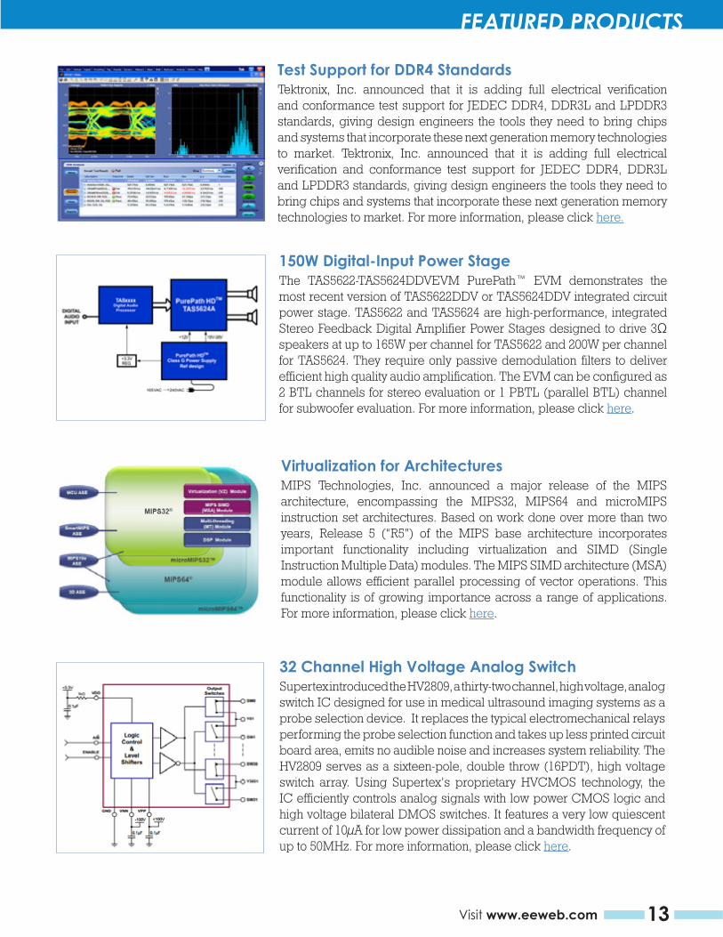
Test Support for DDR4 StandardsTektronix, Inc. announced that it is adding full electrical verification and conformance test support for JEDEC DDR4, DDR3L and LPDDR3 standards, giving design engineers the tools they need to bring chips and systems that incorporate these next generation memory technologies to market. Tektronix, Inc. announced that it is adding full electrical verification and conformance test support for JEDEC DDR4, DDR3L and LPDDR3 standards, giving design engineers the tools they need to bring chips and systems that incorporate these next generation memory technologies to market. For more information, please click here.
150W Digital-Input Power StageThe TAS5622-TAS5624DDVEVM PurePath™ EVM demonstrates the most recent version of TAS5622DDV or TAS5624DDV integrated circuit power stage. TAS5622 and TAS5624 are high-performance, integrated Stereo Feedback Digital Amplifier Power Stages designed to drive 3Ω speakers at up to 165W per channel for TAS5622 and 200W per channel for TAS5624. They require only passive demodulation filters to deliver efficient high quality audio amplification. The EVM can be configured as 2 BTL channels for stereo evaluation or 1 PBTL (parallel BTL) channel for subwoofer evaluation. For more information, please click here.
Virtualization for ArchitecturesMIPS Technologies, Inc. announced a major release of the MIPS architecture, encompassing the MIPS32, MIPS64 and microMIPS instruction set architectures. Based on work done over more than two years, Release 5 (“R5”) of the MIPS base architecture incorporates important functionality including virtualization and SIMD (Single Instruction Multiple Data) modules. The MIPS SIMD architecture (MSA) module allows efficient parallel processing of vector operations. This functionality is of growing importance across a range of applications. For more information, please click here.
32 Channel High Voltage Analog SwitchSupertex introduced the HV2809, a thirty-two channel, high voltage, analog switch IC designed for use in medical ultrasound imaging systems as a probe selection device. It replaces the typical electromechanical relays performing the probe selection function and takes up less printed circuit board area, emits no audible noise and increases system reliability. The HV2809 serves as a sixteen-pole, double throw (16PDT), high voltage switch array. Using Supertex’s proprietary HVCMOS technology, the IC efficiently controls analog signals with low power CMOS logic and high voltage bilateral DMOS switches. It features a very low quiescent current of 10µA for low power dissipation and a bandwidth frequency of up to 50MHz. For more information, please click here.
Optocouplers are the only isolation devices that meet or exceed the IEC 60747-5-5 International Safety Standard for insulation and isolation. Stringent evaluation tests show Avago’s optocouplers deliver outstanding performance on essential safety and deliver exceptional High Voltage protection for your equipment. Alternative isolation technologies such as ADI’s magnetic or TI’s capacitive isolators do not deliver anywhere near the high voltage insulation protection or noise isolation capabilities that optocouplers deliver.
For more details on this subject, read our white paper at: www.avagoresponsecenter.com/672
Avago Technologies Optocouplers
A Superior Technologyfor High Voltage Protection!
Technology You Can Trust
IEC 60747-5-5 Certifi ed
EEWeb PULSE PROJECT
14 EEWeb | Electrical Engineering Community
Taming theChallengesof 20nmCustom/AnalogDesign Samta Bansal
Cadence
Custom and analog designers will lay the foundation for 20nm IC design. However, they face many challenges that arise from manufacturing complexity. The solution lies not just in improving individual tools, but in a new design methodology that allows rapid layout prototyping, in-design signoff, and close collaboration between schematic and layout designers.

EEWeb PULSE PROJECT
15Visit www.eeweb.com
Taming theChallengesof 20nmCustom/AnalogDesign Samta Bansal
Cadence
EEWeb PULSE PROJECT
16 EEWeb | Electrical Engineering Community
Introduction
For many electronics OEMs, particularly those working with mobile applications, the move to the 20nm process node will be irresistible. Early estimates point to a potential 30-50% performance gain, 30% dynamic power savings, and 50% area reduction compared to the 28nm node. Chip complexity may range up to 8-12 billion transistors. With all its benefits, the 20nm node will open the door to a new generation of smaller, faster, more differentiated devices.
The 20nm process node, however, comes with many challenges, and most of the discussion thus far has concentrated on the challenges faced by digital designers1. This white paper focuses on the custom and analog designers who will lay the foundation for 20nm design. Custom designers will produce the standard cells, memories, and I/Os that digital designers will assemble into systems-on-chip (SoCs). Analog designers will create the IP blocks that will be integrated into 20nm SoCs, nearly all of which will be mixed-signal.
All designers face several “big picture” challenges at 20nm. One is simply the investment that’s required. The research firm IBS predicts substantial increases in fab costs, process R&D, mask costs, and design costs with the move from 28nm to 20nm (Figure 1). Profitability may require shipments of 60-100 million units. Finances will thus mandate careful risk considerations.
increasing concerns about mixed-signal design, integration, and verification. Mixed-signal interactions will increase as more and more digital control circuitry is used, and as analog and digital components come into close proximity.
Of most concern to custom/analog designers— and the main topic of this white paper—are the challenges that arise from manufacturing complexity. What is unique about 20nm is the deep and complex interdependency of manufacturing and variability, on top of increasing timing, power, and area challenges. Concerns include the following:
• The use of double patterning (with extra mask layers) so 193nm photolithography equipment can print features at 20nm
• Layout-dependent effects (LDE) in which the layout context—what is placed near to a device—can impact device performance by as much as 30%
• New local interconnect layers
• More than 5,000 design rules, including some new and difficult ones
28nm 20nm
Fab Costs
Process R&D
Mask Costs
Design Costs
$3B
$1.2B
$2M - $3M
$50M - $90M
$4B - $7B
$2.1B - $3B
$5M - $8M
$120M - $500M
Figure 1: Fab, process, mask, and design costs are much higher at 20nm (IBS, May 2011)
Another challenge is design enablement, which mostly represents a worsening of existing concerns. These concerns include time to market, profitability, predictability, low power, complexity, and cost. At 20nm, an increased amount of silicon IP must be obtained from multiple sources, and there will be increasing concerns about mixed-signal design, integration, and verification. Mixed-signal interactions will increase as more and more digital control circuitry is used, and as analog and digital components come into close proximity.
Of most concern to custom/analog designers— and the main topic of this white paper—are the challenges that arise from manufacturing complexity. What is unique about 20nm is the deep and complex interdependency of manufacturing and variability, on top of increasing timing, power, and area challenges. Concerns include the following:
• The use of double patterning (with extra mask layers) so 193nm photolithography equipment can print features at 20nm
• Layout-dependent effects (LDE) in which the layout context—what is placed near to a device—can impact device performance by as much as 30%
• New local interconnect layers
• More than 5,000 design rules, including some new and difficult ones
• Device variation and sensitivity
• A new type of transistor, the FinFET
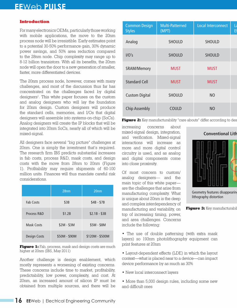
Concerns about manufacturability issues vary according to design style (Figure 2). For example, analog and I/O designers are most concerned about LDE, circuit specifications, and area vs. performance tradeoffs. Memory and standard cell designers are very concerned about density, and as such, double patterning and local interconnect are key concerns.
www.cadence.com 2
Taming the Challenges of 20nm Custom/Analog Design
Another challenge is design enablement, which mostly represents a worsening of existing concerns. These concerns include time to market, profitability, predictability, low power, complexity, and cost. At 20nm, an increased amount of silicon IP must be obtained from multiple sources, and there will be
Multi-Patterned (MPT)
Common DesignStyles
Local Interconnect Layout-DependentEffects (LDE)
Analog
I/O’s
SRAM/Memory
Standard Cell
Custom Digital
Chip Assembly
SHOULD
SHOULD
MUST
MUST
SHOULD
COULD
SHOULD
SHOULD
MUST
MUST
NO
NO
MUST
MUST
SHOULD
SHOULD
COULD
COULD
Figure 2: Key manufacturability “care abouts” differ according to design style
The solution to 20nm custom/analog challenges lies not only in new point tools, but in a new custom design methodology. In this methodology, circuit (schematic) and layout designers will work in close collaboration, and will have the ability to rapidly exchange information. Circuit designers will be able to obtain early parasitic estimates before the layout is completed. The flow will use in-design, signoff-quality engines as opposed to attempting to fix everything during the final signoff stage. And all tools will be “double patterning-aware” and ready for 20nm.
Double Patterning
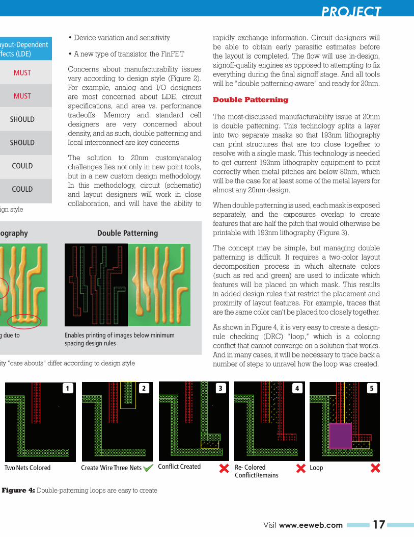
The most-discussed manufacturability issue at 20nm is double patterning. This technology splits a layer into two separate masks so that 193nm lithography can print structures that are too close together to resolve with a single mask. This technology is needed to get current 193nm lithography equipment to print correctly when metal pitches are below 80nm, which will be the case for at least some of the metal layers for almost any 20nm design.
When double patterning is used, each mask is exposed separately, and the exposures overlap to create features that are half the pitch that would otherwise be printable with 193nm lithography (Figure 3).
Conventional Lithography Double Patterning
Geometry features disappearing due to lithography distortion
Enables printing of images below minimum spacing design rules
Figure 3: Double patterning makes it possible to print features that could not be printed with 193nm lithography
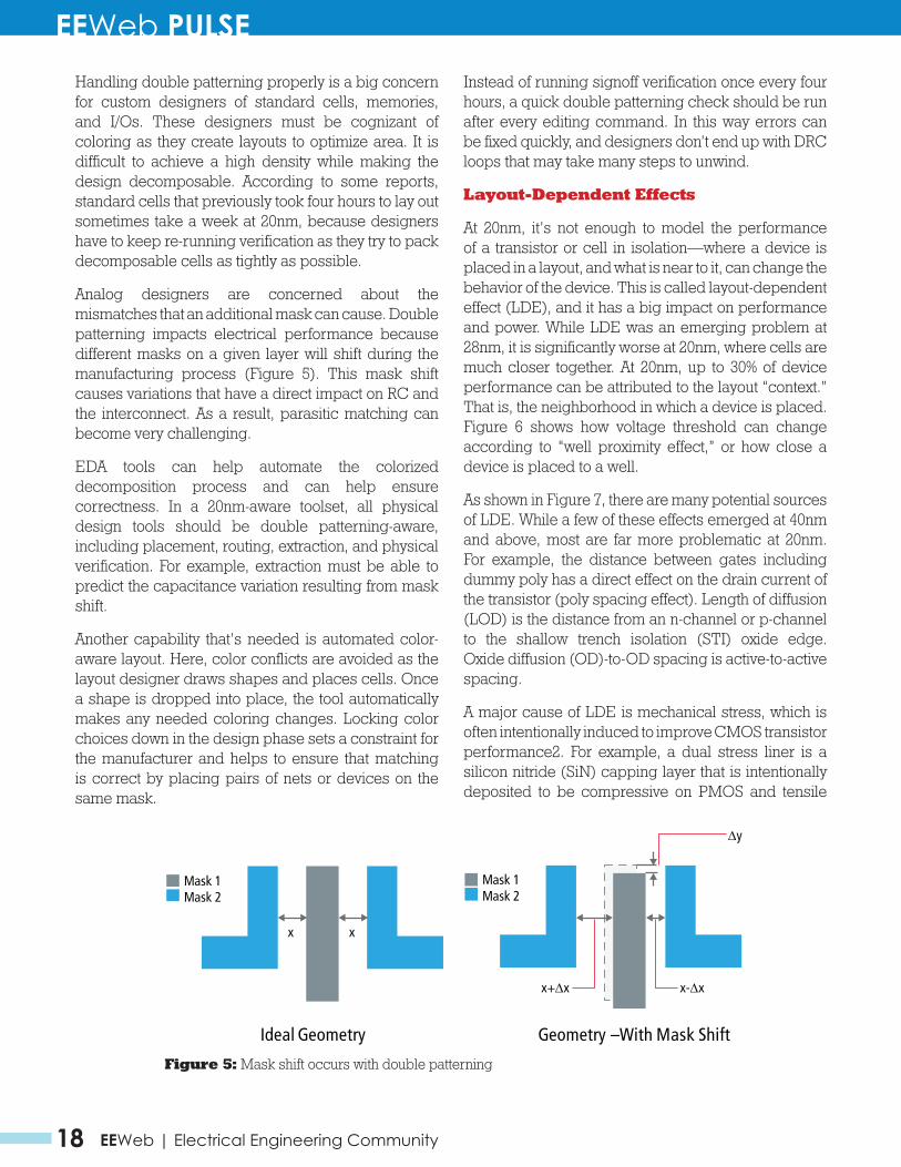
The concept may be simple, but managing double patterning is difficult. It requires a two-color layout decomposition process in which alternate colors (such as red and green) are used to indicate which features will be placed on which mask. This results in added design rules that restrict the placement and proximity of layout features. For example, traces that are the same color can’t be placed too closely together.
www.cadence.com 3
Taming the Challenges of 20nm Custom/Analog Design
Multi-Patterned (MPT)
Common DesignStyles
Local Interconnect Layout-DependentEffects (LDE)
Analog
I/O’s
SRAM/Memory
Standard Cell
Custom Digital
Chip Assembly
SHOULD
SHOULD
MUST
MUST
SHOULD
COULD
SHOULD
SHOULD
MUST
MUST
NO
NO
MUST
MUST
SHOULD
SHOULD
COULD
COULD
Figure 2: Key manufacturability “care abouts” differ according to design style
The solution to 20nm custom/analog challenges lies not only in new point tools, but in a new custom design methodology. In this methodology, circuit (schematic) and layout designers will work in close collaboration, and will have the ability to rapidly exchange information. Circuit designers will be able to obtain early parasitic estimates before the layout is completed. The flow will use in-design, signoff-quality engines as opposed to attempting to fix everything during the final signoff stage. And all tools will be “double patterning-aware” and ready for 20nm.
Double Patterning
The most-discussed manufacturability issue at 20nm is double patterning. This technology splits a layer into two separate masks so that 193nm lithography can print structures that are too close together to resolve with a single mask. This technology is needed to get current 193nm lithography equipment to print correctly when metal pitches are below 80nm, which will be the case for at least some of the metal layers for almost any 20nm design.
When double patterning is used, each mask is exposed separately, and the exposures overlap to create features that are half the pitch that would otherwise be printable with 193nm lithography (Figure 3).
Conventional Lithography Double Patterning
Geometry features disappearing due to lithography distortion
Enables printing of images below minimum spacing design rules
Figure 3: Double patterning makes it possible to print features that could not be printed with 193nm lithography
The concept may be simple, but managing double patterning is difficult. It requires a two-color layout decomposition process in which alternate colors (such as red and green) are used to indicate which features will be placed on which mask. This results in added design rules that restrict the placement and proximity of layout features. For example, traces that are the same color can’t be placed too closely together.
www.cadence.com 3
Taming the Challenges of 20nm Custom/Analog Design
Figure 1: Fab, process, mask and design costs are much higher at 20nm (IBS, May 2011)
Figure 2: Key manufacturability “care abouts” differ according to design style
Figure 3: Key manufacturability “care abouts” differ according to design style
EEWeb PULSE PROJECT
17Visit www.eeweb.com
• Device variation and sensitivity
• A new type of transistor, the FinFET
Concerns about manufacturability issues vary according to design style (Figure 2). For example, analog and I/O designers are most concerned about LDE, circuit specifications, and area vs. performance tradeoffs. Memory and standard cell designers are very concerned about density, and as such, double patterning and local interconnect are key concerns.
The solution to 20nm custom/analog challenges lies not only in new point tools, but in a new custom design methodology. In this methodology, circuit (schematic) and layout designers will work in close collaboration, and will have the ability to
rapidly exchange information. Circuit designers will be able to obtain early parasitic estimates before the layout is completed. The flow will use in-design, signoff-quality engines as opposed to attempting to fix everything during the final signoff stage. And all tools will be “double patterning-aware” and ready for 20nm.
Double Patterning
The most-discussed manufacturability issue at 20nm is double patterning. This technology splits a layer into two separate masks so that 193nm lithography can print structures that are too close together to resolve with a single mask. This technology is needed to get current 193nm lithography equipment to print correctly when metal pitches are below 80nm, which will be the case for at least some of the metal layers for almost any 20nm design.
When double patterning is used, each mask is exposed separately, and the exposures overlap to create features that are half the pitch that would otherwise be printable with 193nm lithography (Figure 3).
The concept may be simple, but managing double patterning is difficult. It requires a two-color layout decomposition process in which alternate colors (such as red and green) are used to indicate which features will be placed on which mask. This results in added design rules that restrict the placement and proximity of layout features. For example, traces that are the same color can’t be placed too closely together.
As shown in Figure 4, it is very easy to create a design-rule checking (DRC) “loop,” which is a coloring conflict that cannot converge on a solution that works. And in many cases, it will be necessary to trace back a number of steps to unravel how the loop was created.
Multi-Patterned (MPT)
Common DesignStyles
Local Interconnect Layout-DependentEffects (LDE)
Analog
I/O’s
SRAM/Memory
Standard Cell
Custom Digital
Chip Assembly
SHOULD
SHOULD
MUST
MUST
SHOULD
COULD
SHOULD
SHOULD
MUST
MUST
NO
NO
MUST
MUST
SHOULD
SHOULD
COULD
COULD
Figure 2: Key manufacturability “care abouts” differ according to design style
The solution to 20nm custom/analog challenges lies not only in new point tools, but in a new custom design methodology. In this methodology, circuit (schematic) and layout designers will work in close collaboration, and will have the ability to rapidly exchange information. Circuit designers will be able to obtain early parasitic estimates before the layout is completed. The flow will use in-design, signoff-quality engines as opposed to attempting to fix everything during the final signoff stage. And all tools will be “double patterning-aware” and ready for 20nm.
Double Patterning
The most-discussed manufacturability issue at 20nm is double patterning. This technology splits a layer into two separate masks so that 193nm lithography can print structures that are too close together to resolve with a single mask. This technology is needed to get current 193nm lithography equipment to print correctly when metal pitches are below 80nm, which will be the case for at least some of the metal layers for almost any 20nm design.
When double patterning is used, each mask is exposed separately, and the exposures overlap to create features that are half the pitch that would otherwise be printable with 193nm lithography (Figure 3).
Conventional Lithography Double Patterning
Geometry features disappearing due to lithography distortion
Enables printing of images below minimum spacing design rules
Figure 3: Double patterning makes it possible to print features that could not be printed with 193nm lithography
The concept may be simple, but managing double patterning is difficult. It requires a two-color layout decomposition process in which alternate colors (such as red and green) are used to indicate which features will be placed on which mask. This results in added design rules that restrict the placement and proximity of layout features. For example, traces that are the same color can’t be placed too closely together.
www.cadence.com 3
Taming the Challenges of 20nm Custom/Analog Design
As shown in Figure 4, it is very easy to create a design-rule checking (DRC) “loop,” which is a coloring conflict that cannot converge on a solution that works. And in many cases, it will be necessary to trace back a number of steps to unravel how the loop was created.
1
Two Nets Colored
2
Create Wire Three Nets
3
Conflict Created
4
Re- ColoredConflict Remains
5
Loop
Figure 4: Double-patterning loops are easy to create
Handling double patterning properly is a big concern for custom designers of standard cells, memories, and I/Os. These designers must be cognizant of coloring as they create layouts to optimize area. It is difficult to achieve a high density while making the design decomposable. According to some reports, standard cells that previously took four hours to lay out sometimes take a week at 20nm, because designers have to keep re-running verification as they try to pack decomposable cells as tightly as possible.
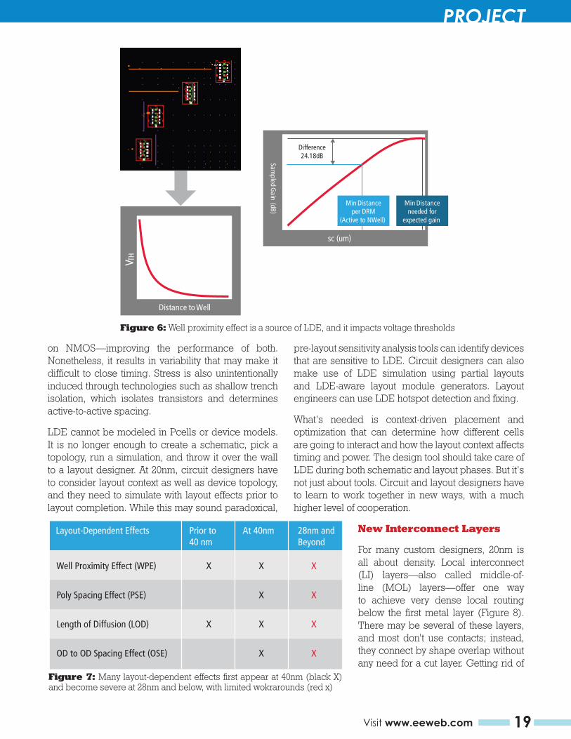
Analog designers are concerned about the mismatches that an additional mask can cause. Double patterning impacts electrical performance because different masks on a given layer will shift during the manufacturing process (Figure 5). This mask shift causes variations that have a direct impact on RC and the interconnect. As a result, parasitic matching can become very challenging.
Mask 1Mask 2
Ideal Geometry
Mask 1Mask 2
x x
x+∆x
∆y
Geometry –With Mask Shift
x-∆x
Figure 5: Mask shift occurs with double patterning
EDA tools can help automate the colorized decomposition process and can help ensure correctness. In a 20nm-aware toolset, all physical design tools should be double patterning‒aware, including placement, routing, extraction, and physical verification. For example, extraction must be able to predict the capacitance variation resulting from mask shift.
Another capability that’s needed is automated color-aware layout. Here, color conflicts are avoided as the layout designer draws shapes and places cells. Once a shape is dropped into place, the tool automatically makes any needed coloring changes. Locking color choices down in the design phase sets a constraint for the manufacturer and helps to ensure that matching is correct by placing pairs of nets or devices on the same mask.
Instead of running signoff verification once every four hours, a quick double patterning check should be run after every editing command. In this way errors can be fixed quickly, and designers don’t end up with DRC loops that may take many steps to unwind.
www.cadence.com 4
Taming the Challenges of 20nm Custom/Analog Design
Figure 2: Key manufacturability “care abouts” differ according to design style
Figure 3: Key manufacturability “care abouts” differ according to design style
Figure 4: Double-patterning loops are easy to create
EEWeb PULSE PROJECT
18 EEWeb | Electrical Engineering Community
Handling double patterning properly is a big concern for custom designers of standard cells, memories, and I/Os. These designers must be cognizant of coloring as they create layouts to optimize area. It is difficult to achieve a high density while making the design decomposable. According to some reports, standard cells that previously took four hours to lay out sometimes take a week at 20nm, because designers have to keep re-running verification as they try to pack decomposable cells as tightly as possible.
Analog designers are concerned about the mismatches that an additional mask can cause. Double patterning impacts electrical performance because different masks on a given layer will shift during the manufacturing process (Figure 5). This mask shift causes variations that have a direct impact on RC and the interconnect. As a result, parasitic matching can become very challenging.
EDA tools can help automate the colorized decomposition process and can help ensure correctness. In a 20nm-aware toolset, all physical design tools should be double patterning-aware, including placement, routing, extraction, and physical verification. For example, extraction must be able to predict the capacitance variation resulting from mask shift.
Another capability that’s needed is automated color-aware layout. Here, color conflicts are avoided as the layout designer draws shapes and places cells. Once a shape is dropped into place, the tool automatically makes any needed coloring changes. Locking color choices down in the design phase sets a constraint for the manufacturer and helps to ensure that matching is correct by placing pairs of nets or devices on the same mask.
Instead of running signoff verification once every four hours, a quick double patterning check should be run after every editing command. In this way errors can be fixed quickly, and designers don’t end up with DRC loops that may take many steps to unwind.
Layout-Dependent Effects
At 20nm, it’s not enough to model the performance of a transistor or cell in isolation—where a device is placed in a layout, and what is near to it, can change the behavior of the device. This is called layout-dependent effect (LDE), and it has a big impact on performance and power. While LDE was an emerging problem at 28nm, it is significantly worse at 20nm, where cells are much closer together. At 20nm, up to 30% of device performance can be attributed to the layout “context.” That is, the neighborhood in which a device is placed. Figure 6 shows how voltage threshold can change according to “well proximity effect,” or how close a device is placed to a well.
As shown in Figure 7, there are many potential sources of LDE. While a few of these effects emerged at 40nm and above, most are far more problematic at 20nm. For example, the distance between gates including dummy poly has a direct effect on the drain current of the transistor (poly spacing effect). Length of diffusion (LOD) is the distance from an n-channel or p-channel to the shallow trench isolation (STI) oxide edge. Oxide diffusion (OD)-to-OD spacing is active-to-active spacing.
A major cause of LDE is mechanical stress, which is often intentionally induced to improve CMOS transistor performance2. For example, a dual stress liner is a silicon nitride (SiN) capping layer that is intentionally deposited to be compressive on PMOS and tensile
As shown in Figure 4, it is very easy to create a design-rule checking (DRC) “loop,” which is a coloring conflict that cannot converge on a solution that works. And in many cases, it will be necessary to trace back a number of steps to unravel how the loop was created.
1
Two Nets Colored
2
Create Wire Three Nets
3
Conflict Created
4
Re- ColoredConflict Remains
5
Loop
Figure 4: Double-patterning loops are easy to create
Handling double patterning properly is a big concern for custom designers of standard cells, memories, and I/Os. These designers must be cognizant of coloring as they create layouts to optimize area. It is difficult to achieve a high density while making the design decomposable. According to some reports, standard cells that previously took four hours to lay out sometimes take a week at 20nm, because designers have to keep re-running verification as they try to pack decomposable cells as tightly as possible.
Analog designers are concerned about the mismatches that an additional mask can cause. Double patterning impacts electrical performance because different masks on a given layer will shift during the manufacturing process (Figure 5). This mask shift causes variations that have a direct impact on RC and the interconnect. As a result, parasitic matching can become very challenging.
Mask 1Mask 2
Ideal Geometry
Mask 1Mask 2
x x
x+∆x
∆y
Geometry –With Mask Shift
x-∆x
Figure 5: Mask shift occurs with double patterning
EDA tools can help automate the colorized decomposition process and can help ensure correctness. In a 20nm-aware toolset, all physical design tools should be double patterning‒aware, including placement, routing, extraction, and physical verification. For example, extraction must be able to predict the capacitance variation resulting from mask shift.
Another capability that’s needed is automated color-aware layout. Here, color conflicts are avoided as the layout designer draws shapes and places cells. Once a shape is dropped into place, the tool automatically makes any needed coloring changes. Locking color choices down in the design phase sets a constraint for the manufacturer and helps to ensure that matching is correct by placing pairs of nets or devices on the same mask.
Instead of running signoff verification once every four hours, a quick double patterning check should be run after every editing command. In this way errors can be fixed quickly, and designers don’t end up with DRC loops that may take many steps to unwind.
www.cadence.com 4
Taming the Challenges of 20nm Custom/Analog Design
Figure 5: Mask shift occurs with double patterning
EEWeb PULSE PROJECT
19Visit www.eeweb.com
on NMOS—improving the performance of both. Nonetheless, it results in variability that may make it difficult to close timing. Stress is also unintentionally induced through technologies such as shallow trench isolation, which isolates transistors and determines active-to-active spacing.
LDE cannot be modeled in Pcells or device models. It is no longer enough to create a schematic, pick a topology, run a simulation, and throw it over the wall to a layout designer. At 20nm, circuit designers have to consider layout context as well as device topology, and they need to simulate with layout effects prior to layout completion. While this may sound paradoxical,
pre-layout sensitivity analysis tools can identify devices that are sensitive to LDE. Circuit designers can also make use of LDE simulation using partial layouts and LDE-aware layout module generators. Layout engineers can use LDE hotspot detection and fixing.
What’s needed is context-driven placement and optimization that can determine how different cells are going to interact and how the layout context affects timing and power. The design tool should take care of LDE during both schematic and layout phases. But it’s not just about tools. Circuit and layout designers have to learn to work together in new ways, with a much higher level of cooperation.
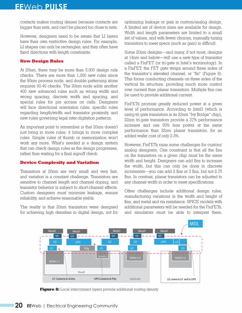
New Interconnect Layers
For many custom designers, 20nm is all about density. Local interconnect (LI) layers—also called middle-of-line (MOL) layers—offer one way to achieve very dense local routing below the first metal layer (Figure 8). There may be several of these layers, and most don’t use contacts; instead, they connect by shape overlap without any need for a cut layer. Getting rid of
Layout-Dependent Effects
At 20nm, it’s not enough to model the performance of a transistor or cell in isolation—where a device is placed in a layout, and what is near to it, can change the behavior of the device. This is called layout-dependent effect (LDE), and it has a big impact on performance and power. While LDE was an emerging problem at 28nm, it is significantly worse at 20nm, where cells are much closer together. At 20nm, up to 30% of device performance can be attributed to the layout “context.” That is, the neighborhood in which a device is placed. Figure 6 shows how voltage threshold can change according to “well proximity effect,” or how close a device is placed to a well.
V TH
Distance to Well
sc (um)
Sampled G
ain (dB)
Min Distanceper DRM
(Active to NWell)
Min Distanceneeded for
expected gain
Difference24.18dB
Figure 6: Well proximity effect is a source of LDE, and it impacts voltage thresholds
As shown in Figure 7, there are many potential sources of LDE. While a few of these effects emerged at 40nm and above, most are far more problematic at 20nm. For example, the distance between gates including dummy poly has a direct effect on the drain current of the transistor (poly spacing effect). Length of diffusion (LOD) is the distance from an n-channel or p-channel to the shallow trench isolation (STI) oxide edge. Oxide diffusion (OD)-to-OD spacing is active-to-active spacing.
Layout-Dependent Effects Prior to40 nm
At 40nm 28nm and Beyond
Well Proximity Effect (WPE)
Poly Spacing Effect (PSE)
Length of Diffusion (LOD)
OD to OD Spacing Effect (OSE)
X
X
X
X
X
X
X
X
X
X
Figure 7: Many layout-dependent effects first appear at 40nm (black X) and become severe at 28nm and below, with limited workarounds (red X)
www.cadence.com 5
Taming the Challenges of 20nm Custom/Analog Design
Figure 6: Well proximity effect is a source of LDE, and it impacts voltage thresholds
Figure 7: Many layout-dependent effects first appear at 40nm (black X) and become severe at 28nm and below, with limited wokrarounds (red x)
EEWeb PULSE PROJECT
20 EEWeb | Electrical Engineering Community
contacts makes routing denser because contacts are bigger than nets, and can’t be placed too close to nets.
However, designers need to be aware that LI layers have their own restrictive design rules. For example, LI shapes can only be rectangles, and they often have fixed directions with length constraints.
New Design Rules
At 20nm, there may be more than 5,000 design rule checks. There are more than 1,000 new rules since the 90nm process node, and double patterning alone requires 30-40 checks. The 20nm node adds another 400 new advanced rules such as wrong width and wrong spacing, discrete width and spacing, and special rules for pin access on cells. Designers will face directional orientation rules, specific rules regarding length/width and transistor proximity, and new rules governing legal inter-digitation patterns.
An important point to remember is that 20nm doesn’t just bring in more rules; it brings in more complex rules. Simple rules of thumb or memorization won’t work any more. What’s needed is a design system that can check design rules as the design progresses, rather than waiting for a final signoff check.
Device Complexity and Variation
Transistors at 20nm are very small and very fast, and variation is a constant challenge. Transistors are sensitive to channel length and channel doping, and transistor behavior is subject to short-channel effects. Custom designers must minimize leakage, ensure reliability, and achieve reasonable yields.
The reality is that 20nm transistors were designed for achieving high densities in digital design, not for
optimizing leakage or gain in custom/analog design. A limited set of device sizes are available for design. Width and length parameters are limited to a small set of values, and with fewer choices, manually tuning transistors to meet specs (such as gain) is difficult.
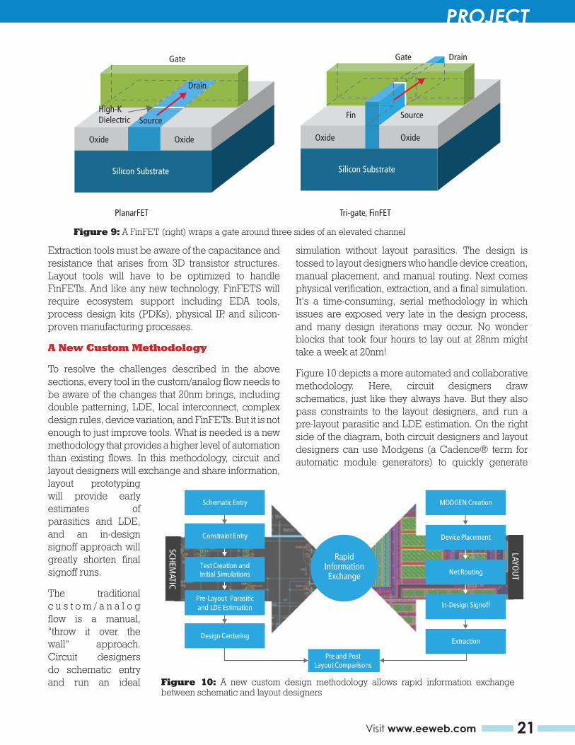
Some 20nm designs—and many, if not most, designs at 14nm and below—will use a new type of transistor called a FinFET (or tri-gate in Intel’s terminology). In a FinFET, the FET gate wraps around three sides of the transistor’s elevated channel, or “fin” (Figure 9). This forms conducting channels on three sides of the vertical fin structure, providing much more control over current than planar transistors. Multiple fins can be used to provide additional current.
FinFETs promise greatly reduced power at a given level of performance. According to Intel3 (which is using tri-gate transistors in its 22nm “Ivy Bridge” chip), 22nm tri-gate transistors provide a 37% performance increase and use 50% less power at the same performance than 32nm planar transistors, for an added wafer cost of only 2-3%.
However, FinFETs raise some challenges for custom/analog designers. One constraint is that all the fins on the transistors on a given chip must be the same width and height. Designers can add fins to increase the width, but this can only be done in discrete increments—you can add 2 fins or 3 fins, but not 2.75 fins. In contrast, planar transistors can be adjusted to any channel width in order to meet specifications.
Other challenges include additional design rules, manufacturing variations in the width and height of fins, and metal and via resistance. SPICE models with additional parameters will be needed for the FinFETs, and simulators must be able to interpret them.
A major cause of LDE is mechanical stress, which is often intentionally induced to improve CMOS transistor performance2. For example, a dual stress liner is a silicon nitride (SiN) capping layer that is intentionally deposited to be compressive on PMOS and tensile on NMOS—improving the performance of both. Nonetheless, it results in variability that may make it difficult to close timing. Stress is also unintentionally induced through technologies such as shallow trench isolation, which isolates transistors and determines active-to-active spacing.
LDE cannot be modeled in Pcells or device models. It is no longer enough to create a schematic, pick a topology, run a simulation, and throw it over the wall to a layout designer. At 20nm, circuit designers have to consider layout context as well as device topology, and they need to simulate with layout effects prior to layout completion. While this may sound paradoxical, pre-layout sensitivity analysis tools can identify devices that are sensitive to LDE. Circuit designers can also make use of LDE simulation using partial layouts and LDE-aware layout module generators. Layout engineers can use LDE hotspot detection and fixing.
What’s needed is context-driven placement and optimization that can determine how different cells are going to interact and how the layout context affects timing and power. The design tool should take care of LDE during both schematic and layout phases. But it’s not just about tools. Circuit and layout designers have to learn to work together in new ways, with a much higher level of cooperation.
New Interconnect Layers
For many custom designers, 20nm is all about density. Local interconnect (LI) layers—also called middle-of-line (MOL) layers—offer one way to achieve very dense local routing below the first metal layer (Figure 8). There may be several of these layers, and most don’t use contacts; instead, they connect by shape overlap without any need for a cut layer. Getting rid of contacts makes routing denser because contacts are bigger than nets, and can’t be placed too close to nets.
Substrate
Nwell
Active ( -)
V0
Active (+)
Poly
LIPO
V0
Metal1
Active (+)
V0
Metal1
Active (+)
LIPO
V0
Metal1
V0
Metal1
LI2
LI1
LI2
LI1
LI2
LI1
LI2
Metal1
Substrate
MOL
Li1 Connects to Active LiPO Connects to Poly
LI1
Li2 connects Li1 and to LiPO
Figure 8: Local interconnect layers provide additional routing density
However, designers need to be aware that LI layers have their own restrictive design rules. For example, LI shapes can only be rectangles, and they often have fixed directions with length constraints.
New Design Rules
At 20nm, there may be more than 5,000 design rule checks. There are more than 1,000 new rules since the 90nm process node, and double patterning alone requires 30-40 checks. The 20nm node adds another 400 new advanced rules such as wrong width and wrong spacing, discrete width and spacing, and special rules for pin access on cells. Designers will face directional orientation rules, specific rules regarding length/width and transistor proximity, and new rules governing legal inter-digitation patterns.
An important point to remember is that 20nm doesn’t just bring in more rules; it brings in more complex rules. Simple rules of thumb or memorization won’t work any more. What’s needed is a design system that can check design rules as the design progresses, rather than waiting for a final signoff check.
www.cadence.com 6
Taming the Challenges of 20nm Custom/Analog Design
Figure 8: Local interconnect layers provide additional routing density
EEWeb PULSE PROJECT
21Visit www.eeweb.com
Extraction tools must be aware of the capacitance and resistance that arises from 3D transistor structures. Layout tools will have to be optimized to handle FinFETs. And like any new technology, FinFETS will require ecosystem support including EDA tools, process design kits (PDKs), physical IP, and silicon-proven manufacturing processes.
A New Custom Methodology
To resolve the challenges described in the above sections, every tool in the custom/analog flow needs to be aware of the changes that 20nm brings, including double patterning, LDE, local interconnect, complex design rules, device variation, and FinFETs. But it is not enough to just improve tools. What is needed is a new methodology that provides a higher level of automation than existing flows. In this methodology, circuit and layout designers will exchange and share information, layout prototyping will provide early estimates of parasitics and LDE, and an in-design signoff approach will greatly shorten final signoff runs.
The traditional c u s t o m / a n a l o g flow is a manual, “throw it over the wall” approach. Circuit designers do schematic entry and run an ideal
simulation without layout parasitics. The design is tossed to layout designers who handle device creation, manual placement, and manual routing. Next comes physical verification, extraction, and a final simulation. It’s a time-consuming, serial methodology in which issues are exposed very late in the design process, and many design iterations may occur. No wonder blocks that took four hours to lay out at 28nm might take a week at 20nm!
Figure 10 depicts a more automated and collaborative methodology. Here, circuit designers draw schematics, just like they always have. But they also pass constraints to the layout designers, and run a pre-layout parasitic and LDE estimation. On the right side of the diagram, both circuit designers and layout designers can use Modgens (a Cadence® term for automatic module generators) to quickly generate
Device Complexity and Variation
Transistors at 20nm are very small and very fast, and variation is a constant challenge. Transistors are sensitive to channel length and channel doping, and transistor behavior is subject to short-channel effects. Custom designers must minimize leakage, ensure reliability, and achieve reasonable yields.
The reality is that 20nm transistors were designed for achieving high densities in digital design, not for optimizing leakage or gain in custom/analog design. A limited set of device sizes are available for design. Width and length parameters are limited to a small set of values, and with fewer choices, manually tuning transistors to meet specs (such as gain) is difficult.
Some 20nm designs—and many, if not most, designs at 14nm and below—will use a new type of transistor called a FinFET (or tri-gate in Intel’s terminology). In a FinFET, the FET gate wraps around three sides of the transistor’s elevated channel, or “fin” (Figure 9). This forms conducting channels on three sides of the vertical fin structure, providing much more control over current than planar transistors. Multiple fins can be used to provide additional current.
Gate
Drain
Source
Oxide Oxide
Silicon Substrate
High-KDielectric
Gate Drain
Oxide
Fin Source
Oxide
Silicon Substrate
PlanarFET Tri-gate, FinFET
Figure 9: A FinFET (right) wraps a gate around three sides of an elevated channel
FinFETs promise greatly reduced power at a given level of performance. According to Intel3 (which is using tri-gate transistors in its 22nm “Ivy Bridge” chip), 22nm tri-gate transistors provide a 37% performance increase and use 50% less power at the same performance than 32nm planar transistors, for an added wafer cost of only 2-3%.
However, FinFETs raise some challenges for custom/analog designers. One constraint is that all the fins on the transistors on a given chip must be the same width and height. Designers can add fins to increase the width, but this can only be done in discrete increments—you can add 2 fins or 3 fins, but not 2.75 fins. In contrast, planar transistors can be adjusted to any channel width in order to meet specifications.
Other challenges include additional design rules, manufacturing variations in the width and height of fins, and metal and via resistance. SPICE models with additional parameters will be needed for the FinFETs, and simulators must be able to interpret them. Extraction tools must be aware of the capacitance and resistance that arises from 3D transistor structures. Layout tools will have to be optimized to handle FinFETs. And like any new technology, FinFETS will require ecosystem support including EDA tools, process design kits (PDKs), physical IP, and silicon-proven manufacturing processes.
A New Custom Methodology
To resolve the challenges described in the above sections, every tool in the custom/analog flow needs to be aware of the changes that 20nm brings, including double patterning, LDE, local interconnect, complex design rules, device variation, and FinFETs. But it is not enough to just improve tools. What is needed is a new methodology that provides a higher level of automation than existing flows. In this methodology, circuit and layout designers will exchange and share information, layout prototyping will provide early estimates of parasitics and LDE, and an in-design signoff approach will greatly shorten final signoff runs.
www.cadence.com 7
Taming the Challenges of 20nm Custom/Analog Design
The traditional custom/analog flow is a manual, “throw it over the wall” approach. Circuit designers do schematic entry and run an ideal simulation without layout parasitics. The design is tossed to layout designers who handle device creation, manual placement, and manual routing. Next comes physical verification, extraction, and a final simulation. It’s a time-consuming, serial methodology in which issues are exposed very late in the design process, and many design iterations may occur. No wonder blocks that took four hours to lay out at 28nm might take a week at 20nm!
Figure 10 depicts a more automated and collaborative methodology. Here, circuit designers draw schematics, just like they always have. But they also pass constraints to the layout designers, and run a pre-layout parasitic and LDE estimation. On the right side of the diagram, both circuit designers and layout designers can use Modgens (a Cadence® term for automatic module generators) to quickly generate layouts for structures such as differential pairs, current mirrors, and resistor arrays. While not a final “DRC-clean” layout, these automatically generated layouts allow accurate physical effects to be extracted, analyzed, and simulated. Modules can then be fed into an analog placer and assembled into a floorplan.
Pre and Post Layout Comparisons
LAYOUT
SCHEMATIC
MODGEN Creation
Device Placement
Net Routing
Extraction
Constraint Entry
and LDE Estimation
Test Creation andInitial Simulations
Design Centering
Schematic Entry
RapidInformationExchange
In-Design SignoffPre-Layout Parasitic
Figure 10: A new custom design methodology allows rapid information exchange between schematic and layout designers
Layout engineers then perform device placement, routing, in-design signoff, and extraction. In short, the basic roles of circuit designers and layout designers remain the same, but there is an ongoing and rapid exchange of information and a high degree of collaboration. Constraints flow easily between the schematic and layout environments.
Automatic module generators help enable “rapid layout prototyping,” which is the ability to quickly generate an extracted layout view so circuit designers can run simulations with real parasitic and LDE information. In this way, the electrical and mismatch problems that might be caused by layout effects can be spotted and remedied early in the design cycle. The module generators, however, must be ready for 20nm, with place-and-route engine support for 20nm design rules, complex abutment support, array-based FinFET configurations, coloring for double patterning, and LDE awareness.
Another approach for bringing physical effects into initial simulations is incremental design. Here, designers lay out the pieces they care about with assisted or full automation, and gather as much physical and electrical information as they can. This results in a partial layout extraction. The emphasis is on placement rather than routing. The point is that designers are not taking the time to do a full layout, just what’s necessary to generate the desired parasitic information.
Finally, in-design signoff is a must at 20nm. If a designer makes a mistake during layout, the feedback should come immediately, not four hours or a month later. Otherwise many design iterations may be needed for each block, with each iteration taking longer than it took to do the original design. There are two types of interactive editing checks that can help avoid those iterations. One is “in-edit checking,” which warns of errors while geometry is being created. Another is “post-edit signoff-quality checking,” which exercises a more robust check after each edit is completed.
www.cadence.com 8
Taming the Challenges of 20nm Custom/Analog Design
Figure 10: A new custom design methodology allows rapid information exchange between schematic and layout designers
Figure 9: A FinFET (right) wraps a gate around three sides of an elevated channel
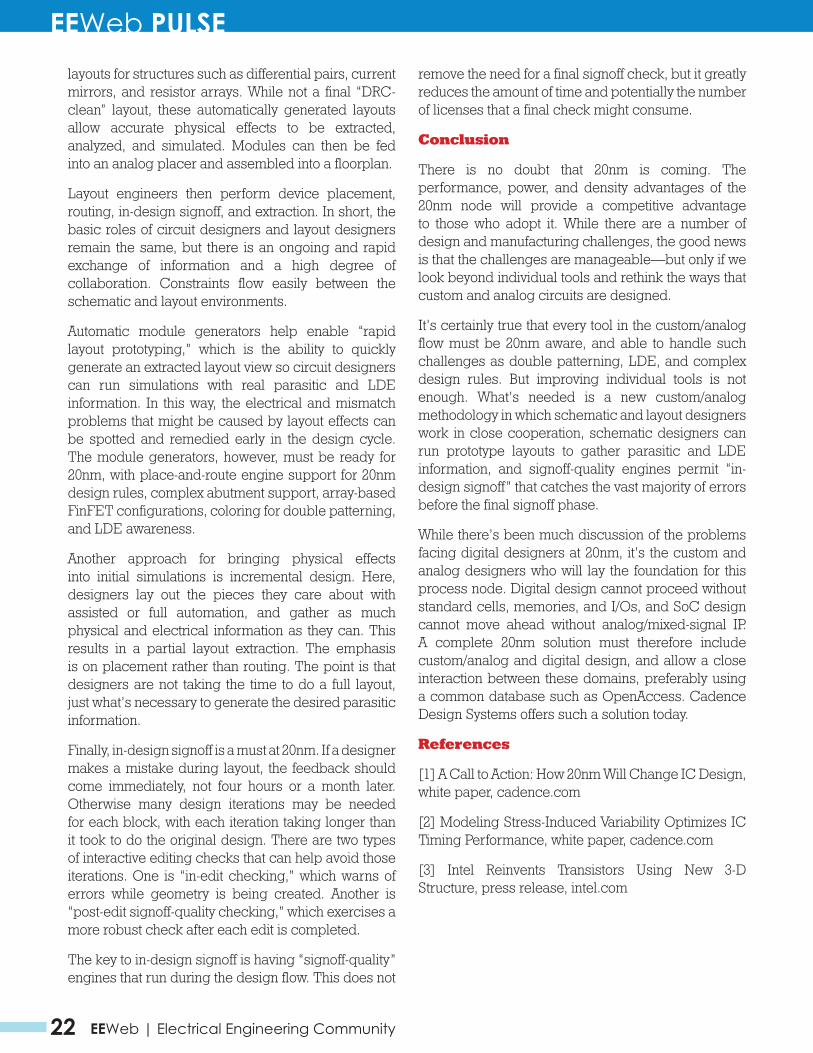
EEWeb PULSE PROJECT
22 EEWeb | Electrical Engineering Community
layouts for structures such as differential pairs, current mirrors, and resistor arrays. While not a final “DRC-clean” layout, these automatically generated layouts allow accurate physical effects to be extracted, analyzed, and simulated. Modules can then be fed into an analog placer and assembled into a floorplan.
Layout engineers then perform device placement, routing, in-design signoff, and extraction. In short, the basic roles of circuit designers and layout designers remain the same, but there is an ongoing and rapid exchange of information and a high degree of collaboration. Constraints flow easily between the schematic and layout environments.
Automatic module generators help enable “rapid layout prototyping,” which is the ability to quickly generate an extracted layout view so circuit designers can run simulations with real parasitic and LDE information. In this way, the electrical and mismatch problems that might be caused by layout effects can be spotted and remedied early in the design cycle. The module generators, however, must be ready for 20nm, with place-and-route engine support for 20nm design rules, complex abutment support, array-based FinFET configurations, coloring for double patterning, and LDE awareness.
Another approach for bringing physical effects into initial simulations is incremental design. Here, designers lay out the pieces they care about with assisted or full automation, and gather as much physical and electrical information as they can. This results in a partial layout extraction. The emphasis is on placement rather than routing. The point is that designers are not taking the time to do a full layout, just what’s necessary to generate the desired parasitic information.
Finally, in-design signoff is a must at 20nm. If a designer makes a mistake during layout, the feedback should come immediately, not four hours or a month later. Otherwise many design iterations may be needed for each block, with each iteration taking longer than it took to do the original design. There are two types of interactive editing checks that can help avoid those iterations. One is “in-edit checking,” which warns of errors while geometry is being created. Another is “post-edit signoff-quality checking,” which exercises a more robust check after each edit is completed.
The key to in-design signoff is having “signoff-quality” engines that run during the design flow. This does not
remove the need for a final signoff check, but it greatly reduces the amount of time and potentially the number of licenses that a final check might consume.
Conclusion
There is no doubt that 20nm is coming. The performance, power, and density advantages of the 20nm node will provide a competitive advantage to those who adopt it. While there are a number of design and manufacturing challenges, the good news is that the challenges are manageable—but only if we look beyond individual tools and rethink the ways that custom and analog circuits are designed.
It’s certainly true that every tool in the custom/analog flow must be 20nm aware, and able to handle such challenges as double patterning, LDE, and complex design rules. But improving individual tools is not enough. What’s needed is a new custom/analog methodology in which schematic and layout designers work in close cooperation, schematic designers can run prototype layouts to gather parasitic and LDE information, and signoff-quality engines permit “in-design signoff” that catches the vast majority of errors before the final signoff phase.
While there’s been much discussion of the problems facing digital designers at 20nm, it’s the custom and analog designers who will lay the foundation for this process node. Digital design cannot proceed without standard cells, memories, and I/Os, and SoC design cannot move ahead without analog/mixed-signal IP. A complete 20nm solution must therefore include custom/analog and digital design, and allow a close interaction between these domains, preferably using a common database such as OpenAccess. Cadence Design Systems offers such a solution today.
References
[1] A Call to Action: How 20nm Will Change IC Design, white paper, cadence.com
[2] Modeling Stress-Induced Variability Optimizes IC Timing Performance, white paper, cadence.com
[3] Intel Reinvents Transistors Using New 3-D Structure, press release, intel.com

Lose all the wires, keep all the dataMicroStrain’s new LXRS™ Wireless Sensing System offers 100% data throughput under most operating conditions
Our new LXRS™ Wireless Sensing System includes:• Losslesswirelesscommunicationsprotocolsprovide100%packetsuccessrate• Extendedrangeradiolinkto2km• Scalablewirelesssensornetworkssupportcontinuous,burst,andhybridsamplingmodes• Timesynchronizedto+/-32microseconds
Little Sensors, Big Ideas®
Call800.449.3878orvisitusonlineatwww.microstrain.com
TolearnmoreaboutourLXRSWirelessSensorNetworks,scanherefordemovideo
With Lossless ProtocolWithout Lossless Protocol
LXRS®
MStrainLXRS 8.5x5.5.indd 1 9/28/12 11:55 AM
Electric
al Engine
ering C
ommunity
EEWeb ARTICLES
JOBS
COMMUNITY
DEVELOPMENT TOOLS
Dave BaarmanDirector Of
Advanced Technologies
Making WirelessTruly Wireless:
Need For UniversalWireless Power
Solution
"Sed ut perspiciatis unde omnis
iste natus error sit voluptatem
accusantium doloremque
laudantium, totam rem aperiam,
eaque ipsa quae ab illo inventore
veritatis et quasi architecto beatae vitae
dicta sunt explicabo. Nemo enim ipsam
voluptatem quia voluptas sit aspernatur aut odit
aut fugit, sed quia consequuntur magni dolores eos
qui ratione voluptatem sequi nesciunt. Neque porro
quisquam est, qui dolorem ipsum quia dolor sit amet, consectetur,
adipisci velit, sed quia non numquam eius modi tempora incidunt ut
labore et dolore magnam aliquam quaerat voluptatem. Ut enim ad
minima veniam, quis nostrum exercitationem ullam corporis suscipit
laboriosam, nisi ut aliquid ex ea commodi consequatur? Quis autem
www.eeweb.comJOIN TODAY

Dual 15A/Single 30A Step-Down Power ModuleISL8225MThe ISL8225M is a fully-encapsulated step-down switching power supply that can deliver up to 100W output power from a small 17mm square PCB footprint. The two 15A outputs may be used independently or combined to deliver a single 30A output. Designing a high-performance board-mounted power supply has never been simpler -- only a few external components are needed to create a very dense and reliable power solution.
Automatic current sharing and phase interleaving allow up to six modules to be paralleled for 180A output capability. 1.5% output voltage accuracy, differential remote voltage sensing and fast transient response create a very high-performance power system. Built-in output over-voltage, over-current and over-temperature protection enhance system reliability.
The ISL8225M is available in a thermally-enhanced QFN package. Excellent efficiency and low thermal resistance permit full power operation without heat sinks or fans. In addition, the QFN package with external leads permits easy probing and visual solder inspection.
Related Resources• See AN1789 “ISL8225MEVAL2Z 6-Phase, 90A Evaluation
Board Setup Procedure”
• See AN1790 “ISL8225MEVAL3Z 30A, Single Output Evaluation Board Setup Procedure”
• See AN1793, “ISL8225MEVAL4Z Dual 15A/Optional 30A Cascadable Evaluation Board”
• See ISL8225M 110A Thermal Performance Video
Features• Fully-encapsulated dual step-down switching power supply
• Up to 100W output from a 17mm square PCB footprint
• Dual 15A or single 30A output
• Up to 95% conversion efficiency
• 4.5V to 20V input voltage range
• 0.6V to 6V output voltage range
• 1.5% output voltage accuracy with differential remote sensing
• Up to six modules may be paralleled to support 180A output current
• Output over-voltage, over-current and over-temperature protection
• Full power operation without heat sinks or fans
• QFN package with exposed leads permits easy probing and visual solder inspection
Applications• Computing, networking and telecom infrastructure
equipment
• Industrial and medical equipment
• General purpose point-of-load (POL) power
FIGURE 1. COMPLETE 30A STEP-DOWN POWER SUPPLY FIGURE 2. SMALL FOOTPRINT WITH HIGH POWER DENSITY
[email protected] TO 20VVOUT
4.7µF
4x22µF
ISL8225M
VIN1
VSEN2-
VSEN1+EN/FF1EN/FF2
VMON2
VMON1
SGN
D
PGN
D
VOUT1
VSEN1-
MO
DE
COMP2
COMP1
VIN
OFF 1kΩ5x100µF
470pF
1kΩ
VCC
RSET
NOTE: ALL PINS NOT SHOWN ARE FLOATING.
VIN2 VOUT2VIN2
ON
17mm 17mm
7.5mm
December 3, 2012FN7822.0
Intersil (and design) is a registered trademark of Intersil Americas Inc. Copyright Intersil Americas Inc. 2012All Rights Reserved. All other trademarks mentioned are the property of their respective owners.
Get the Datasheet and Order Eval Boards
http://www.intersil.com
EEWeb PULSE SPECIAL FEATURE
26 EEWeb | Electrical Engineering Community
Episode 2.2Supporting MCUsin an RTOS

EEWeb PULSE SPECIAL FEATURE
27Visit www.eeweb.com
Episode 2.2Supporting MCUsin an RTOS
In this episode of MCU Wars, Richard Barry and Jean Labross continue the discussion about the nuances of developing in an RTOS. The discussion ranges from the challenges of RTOS developers have in supporting MCUs to reasons why an engineer should not try writ-ing their own RTOS.
This series was filmed at DevCon 2012 by Renesas in Anaheim, California. DevCon pro-vides an environment for valuable technical information exchange and access to Renesas’ technology experts and partners from around the world.
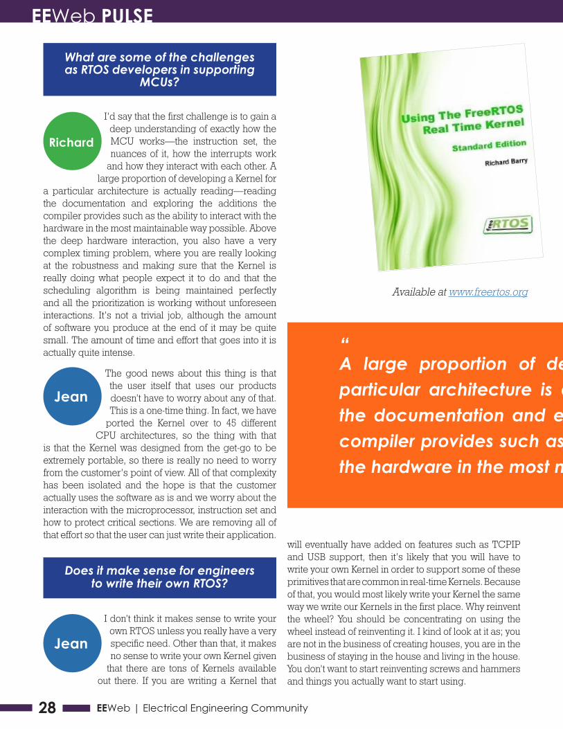
EEWeb PULSE SPECIAL FEATURE
28 EEWeb | Electrical Engineering Community
I’d say that the first challenge is to gain a deep understanding of exactly how the MCU works—the instruction set, the nuances of it, how the interrupts work
and how they interact with each other. A large proportion of developing a Kernel for
a particular architecture is actually reading—reading the documentation and exploring the additions the compiler provides such as the ability to interact with the hardware in the most maintainable way possible. Above the deep hardware interaction, you also have a very complex timing problem, where you are really looking at the robustness and making sure that the Kernel is really doing what people expect it to do and that the scheduling algorithm is being maintained perfectly and all the prioritization is working without unforeseen interactions. It’s not a trivial job, although the amount of software you produce at the end of it may be quite small. The amount of time and effort that goes into it is actually quite intense.
The good news about this thing is that the user itself that uses our products doesn’t have to worry about any of that. This is a one-time thing. In fact, we have
ported the Kernel over to 45 different CPU architectures, so the thing with that
is that the Kernel was designed from the get-go to be extremely portable, so there is really no need to worry from the customer’s point of view. All of that complexity has been isolated and the hope is that the customer actually uses the software as is and we worry about the interaction with the microprocessor, instruction set and how to protect critical sections. We are removing all of that effort so that the user can just write their application.
What are some of the challenges as RTOS developers in supporting
MCUs?
Does it make sense for engineers to write their own RTOS?
I don’t think it makes sense to write your own RTOS unless you really have a very specific need. Other than that, it makes no sense to write your own Kernel given
that there are tons of Kernels available out there. If you are writing a Kernel that
Jean
Richard
Jean
will eventually have added on features such as TCPIP and USB support, then it’s likely that you will have to write your own Kernel in order to support some of these primitives that are common in real-time Kernels. Because of that, you would most likely write your Kernel the same way we write our Kernels in the first place. Why reinvent the wheel? You should be concentrating on using the wheel instead of reinventing it. I kind of look at it as; you are not in the business of creating houses, you are in the business of staying in the house and living in the house. You don’t want to start reinventing screws and hammers and things you actually want to start using.
A large proportion of developing a Kernel for a particular architecture is actually reading—reading the documentation and exploring the additions the compiler provides such as the ability to interact with the hardware in the most maintainable way possible.
“
Available at www.freertos.org

EEWeb PULSE SPECIAL FEATURE
29Visit www.eeweb.com
If I was managing a team that wanted to write their own RTOS, I would say, “Fine. Do it. But do it on your own time, not on mine,” because I don’t want to
pay for something that isn’t going to work as well as products that I can get
off the shelf. Even free products like mine; why would
What advice do you have for project managers willing to write
their own RTOS?
Richard
you write your own when you can get something that’s free, commercial quality, supported, around for eight years, is known to be really robust and is there for you instantly. Why would write your own? It is an intellectual challenge and I can understand the enjoyment of it, but don’t do it on my time!
The only comment I would have there is that you say it’s a commercial-grade product and it’s supported, but support is not free. The product is free but your
hours are not.
I’m going to have to agree and disagree with that. The support is free, but my hours are not. I don’t charge the customer for my hours. There is a
commercial version of FreeRTOS that comes with a support contract. A lot of
companies, for legal reasons, won’t have software in their product unless there is a written contract, so if you want a support contract, you can have that right if you want to.
Correct—but you have to purchase that separately. In [Micrium’s] case, when you purchase our software, not only does the source-code come with it, but
also a full-year support contract for our product. It’s all included.
A large proportion of developing a Kernel for a particular architecture is actually reading—reading the documentation and exploring the additions the compiler provides such as the ability to interact with the hardware in the most maintainable way possible.
”
Jean
Richard
Jean
Continued in Episode 3...
To view this episode of MCU Wars and other EEWeb videos:
Click Here
Available at www.micrium.com

EEWeb PULSE TECH ARTICLE
30 EEWeb | Electrical Engineering Community
Nicholas Abi-SamraVice President of Quanta Technologies
DistributionSystems
Part 2
Automation &Optimization
Vice President, Asset Management - Quanta Technology3

EEWeb PULSE TECH ARTICLE
31Visit www.eeweb.com
Nicholas Abi-SamraVice President of Quanta Technologies
DistributionSystems
Part 2
Automation &Optimization
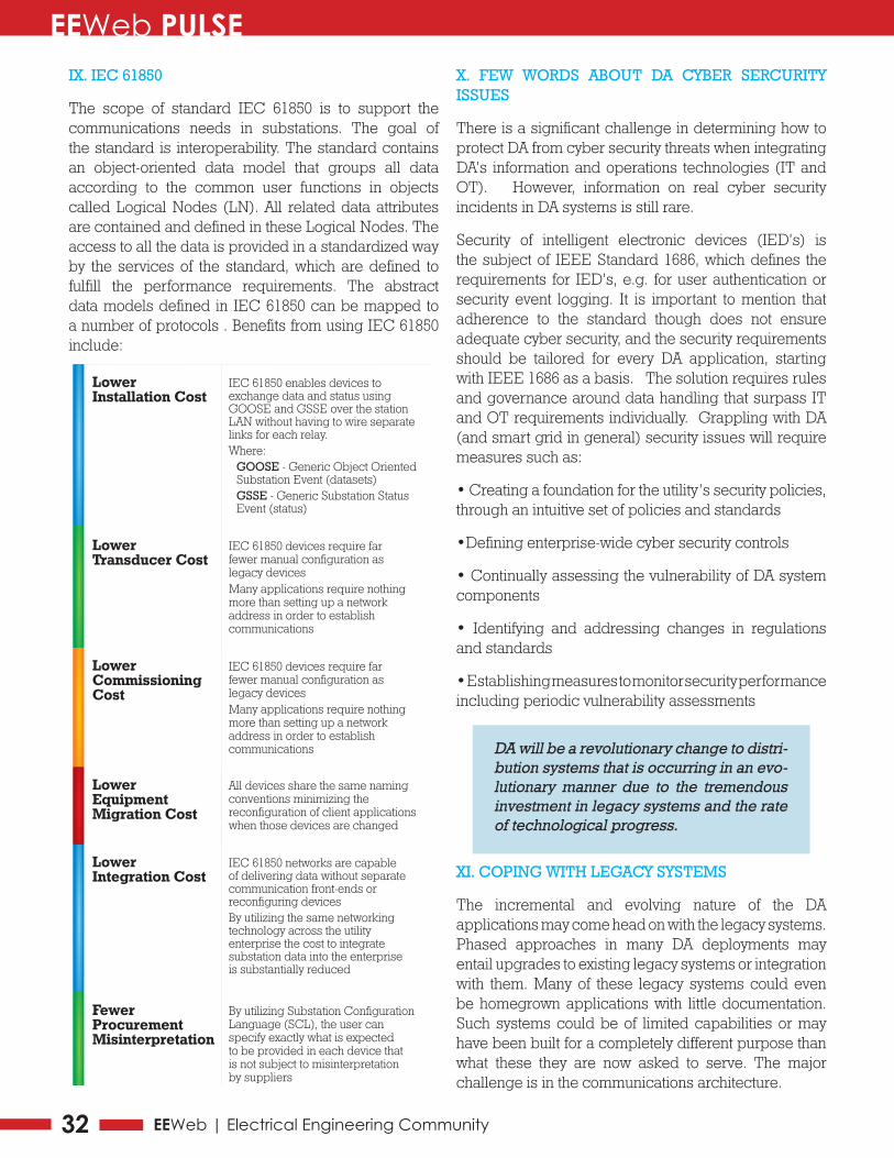
EEWeb PULSE TECH ARTICLE
32 EEWeb | Electrical Engineering Community
IX. IEC 61850
The scope of standard IEC 61850 is to support the communications needs in substations. The goal of the standard is interoperability. The standard contains an object-oriented data model that groups all data according to the common user functions in objects called Logical Nodes (LN). All related data attributes are contained and defined in these Logical Nodes. The access to all the data is provided in a standardized way by the services of the standard, which are defined to fulfill the performance requirements. The abstract data models defined in IEC 61850 can be mapped to a number of protocols . Benefits from using IEC 61850 include:
X. FEW WORDS ABOUT DA CYBER SERCURITY ISSUES
There is a significant challenge in determining how to protect DA from cyber security threats when integrating DA’s information and operations technologies (IT and OT). However, information on real cyber security incidents in DA systems is still rare.
Security of intelligent electronic devices (IED’s) is the subject of IEEE Standard 1686, which defines the requirements for IED’s, e.g. for user authentication or security event logging. It is important to mention that adherence to the standard though does not ensure adequate cyber security, and the security requirements should be tailored for every DA application, starting with IEEE 1686 as a basis. The solution requires rules and governance around data handling that surpass IT and OT requirements individually. Grappling with DA (and smart grid in general) security issues will require measures such as:
• Creating a foundation for the utility’s security policies, through an intuitive set of policies and standards
•Defining enterprise-wide cyber security controls
• Continually assessing the vulnerability of DA system components
• Identifying and addressing changes in regulations and standards
• Establishing measures to monitor security performance including periodic vulnerability assessments
LowerInstallation Cost
LowerTransducer Cost
LowerCommissioningCost
LowerEquipmentMigration Cost
IEC 61850 enables devices toexchange data and status usingGOOSE and GSSE over the stationLAN without having to wire separatelinks for each relay.Where:
GOOSE - Generic Object OrientedSubstation Event (datasets)GSSE - Generic Substation StatusEvent (status)
IEC 61850 devices require farfewer manual configuration aslegacy devicesMany applications require nothingmore than setting up a networkaddress in order to establishcommunications
IEC 61850 devices require farfewer manual configuration aslegacy devicesMany applications require nothingmore than setting up a networkaddress in order to establishcommunications
All devices share the same namingconventions minimizing the reconfiguration of client applicationswhen those devices are changed
FewerProcurementMisinterpretation
By utilizing Substation ConfigurationLanguage (SCL), the user canspecify exactly what is expectedto be provided in each device thatis not subject to misinterpretationby suppliers
LowerIntegration Cost
IEC 61850 networks are capableof delivering data without separatecommunication front-ends orreconfiguring devicesBy utilizing the same networkingtechnology across the utilityenterprise the cost to integratesubstation data into the enterpriseis substantially reduced
XI. COPING WITH LEGACY SYSTEMS
The incremental and evolving nature of the DA applications may come head on with the legacy systems. Phased approaches in many DA deployments may entail upgrades to existing legacy systems or integration with them. Many of these legacy systems could even be homegrown applications with little documentation. Such systems could be of limited capabilities or may have been built for a completely different purpose than what these they are now asked to serve. The major challenge is in the communications architecture.
DA will be a revolutionary change to distri-bution systems that is occurring in an evo-lutionary manner due to the tremendous investment in legacy systems and the rate of technological progress.
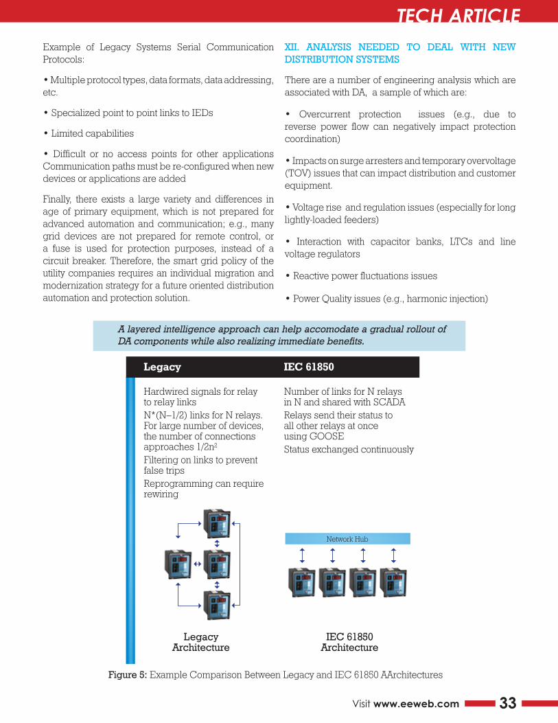
EEWeb PULSE TECH ARTICLE
33Visit www.eeweb.com
Example of Legacy Systems Serial Communication Protocols:
• Multiple protocol types, data formats, data addressing, etc.
• Specialized point to point links to IEDs
• Limited capabilities
• Difficult or no access points for other applications Communication paths must be re-configured when new devices or applications are added
Finally, there exists a large variety and differences in age of primary equipment, which is not prepared for advanced automation and communication; e.g., many grid devices are not prepared for remote control, or a fuse is used for protection purposes, instead of a circuit breaker. Therefore, the smart grid policy of the utility companies requires an individual migration and modernization strategy for a future oriented distribution automation and protection solution.
XII. ANALYSIS NEEDED TO DEAL WITH NEW DISTRIBUTION SYSTEMS
There are a number of engineering analysis which are associated with DA, a sample of which are:
• Overcurrent protection issues (e.g., due to reverse power flow can negatively impact protection coordination)
• Impacts on surge arresters and temporary overvoltage (TOV) issues that can impact distribution and customer equipment.
• Voltage rise and regulation issues (especially for long lightly-loaded feeders)
• Interaction with capacitor banks, LTCs and line voltage regulators
• Reactive power fluctuations issues
• Power Quality issues (e.g., harmonic injection)
LegacyArchitecture
IEC 61850Architecture
Number of links for N relaysin N and shared with SCADARelays send their status toall other relays at onceusing GOOSEStatus exchanged continuously
Hardwired signals for relayto relay linksN*(N–1/2) links for N relays.For large number of devices,the number of connectionsapproaches 1/2n2
Filtering on links to preventfalse tripsReprogramming can requirerewiring
Legacy IEC 61850
Network Hub
Figure 5: Example Comparison Between Legacy and IEC 61850 AArchitectures
A layered intelligence approach can help accomodate a gradual rollout of DA components while also realizing immediate benefits.
EEWeb PULSE TECH ARTICLE
34 EEWeb | Electrical Engineering Community
• Voltage unbalance due to significant proliferation of single-phase (residential type) PV
• Power factor issues which may impact feeder losses
XIII. DA ASSET MANAGEMENT APPLICATIONS
Distribution Automation (DA) provides the utilities means and capabilities to track the performance of distribution assets (transformers, cables, breakers, etc .) in a way which has not been possible before. Equipment loading information, operation history and event characteristics which can be tracked can all provide intelligence on the condition of assets. Such intelligence can be utilized by the asset owners and operators to make more educated and smarter decisions about maintenance programs and asset replacement strategies. This is especially valuable for those assets which have been in operation for many decades (a.k.a, aging assets).
Specifically, some of Asset Management Systems which are empowered by DA are:
• Advanced equipment diagnostics to characterize the condition of distribution system assets
• Advanced methods to determine remaining lifetime of equipment
• Advanced testing techniques to support asset condition assessments
• Decision making tools based on equipment condition for system configuration and management
XIV. CONCLUDING REMARKS
Developing a smart grid through improved DA can improve network efficiency and increase return on investment for electricity distribution utilities. Many DA technologies are now commercially available from a large number of manufacturers. It is the opinion of this this writer that in five years, by the year 2018, the global DA market can be north of $25 billion with Asia Pacific accounting for about a third of that. In USA, the DA market growth will be driven by needs to modernize an aging infrastructure and the need for increasing reliability. In emerging economies, which are encouraging investment in energy grids, intelligent hardware and system efficiency improvements will be the more prevalent drivers.
DA applications have been successfully be deployed in many areas, such as:
• Asset management applications based on the
condition of the distribution assets
• Peak load management in the case of emergencies
• System restoration after failure (e.g., fault location, incipient fault detection (and location) and automated switching on feeders )
• System efficiency improvements (e.g., detecting losses, including non-technical losses and voltage /var control to reduce losses)
Finally, DA has become more important in facilitation of the integration of renewable distributed generation. Through improving energy efficiency, DA can provide opportunities for reduction of greenhouse gasses in electricity generation.
For Part 1 of this Article - click here.
For Part 2 of this Article - click here.
About the Author
Nicholas is a Vice President at Quanta Technology, and leads the Asset Management practice area. He and his team help utilities better manage and modernize their assets at lower total lifecycle cost.
Before Quanta Technology, Nicholas was at Accenture, the Electric Power Research Institute (EPRI) and Westinghouse. At Accenture he served as a Senior Manager at the Smart Grid Services, and developed a number of smart grid analytics and tools for grid modernization. At EPRI, he was a Senior Technical Executive and served as the Director of Transmission and Grid Operations and Planning. At Westinghouse, he was a Westinghouse Fellow Engineer, Westinghouse’s highest technical position) and managed a number engineering groups.
Nicholas is the Chairman of the IEEE Power and Energy Society and the Power Electronics Societies in San Diego, CA. He has over 60 technical papers and articles. He served as the General Chair and Technical Session Coordinator of the IEEE Power & Energy (PES) 2012 General Meeting.
Nicholas was the principal investigator into most of the major grid blackouts, both in the USA and abroad. He is an expert in dealing with aging assets and the effects of extreme weather on power systems.

EEWeb PULSE TECH ARTICLE
35Visit www.eeweb.com
NXP is a leader in low power capacitance touch sensors, which work based on the fact that the human body can serve as one of the capacitive plates in parallel to the second plate, connected to the input of the NXP capacitive sensor device.
Thanks to a patented auto-calibration technology, the capacitive sensors can detect changes in capacitance and continually adjust to the environment. Things such as dirt, humidity, freezing temperatures, or damage to the electrode do not affect the device function. The rise of touch sensors in modern electronics has become a worldwide phenomenon, and with NXP’s low power capacitive sensors it’s never been easier to create the future.
Learn more at: touch.interfacechips.com
World’s lowest power capacitivesensors with auto-calibration