EEWeb Pulse - Issue 27, 2012
21
PULSE EEWeb.com Issue 27 January 3, 2012 Robin McCarty Senior R&D Engineer Electrical Engineering Community EEWeb
description
Interview with Robin McCarty - Marlow Industries; Timing ICs Keep Beat with Needs of Today’s Embedded Market; Millimeter Scale Energy Harvesting Based Sensors; RTZ - Return to Zero Comic
Transcript of EEWeb Pulse - Issue 27, 2012
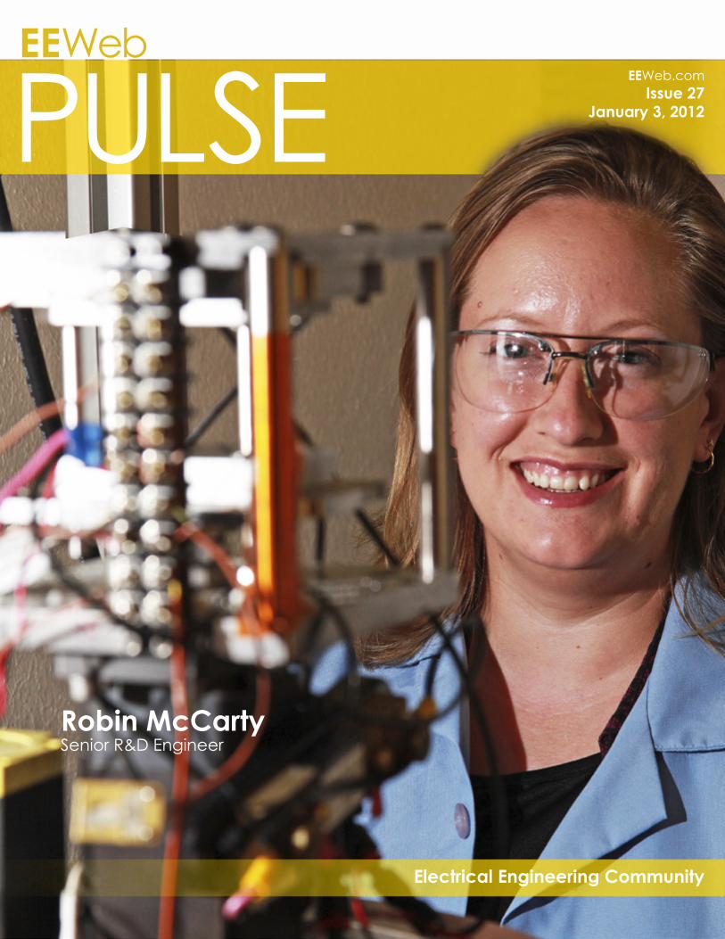
PULSE EEWeb.comIssue 27
January 3, 2012
Robin McCarty Senior R&D Engineer
Electrical Engineering Community
EEWeb

Digi-Key is an authorized distributor for all supplier partners. New products added daily. © 2011 Digi-Key Corporation, 701 Brooks Ave. South, Thief River Falls, MN 56701, USADigi-Key is an authorized distributor for all supplier partners. New products added daily.
www.digikey.com/techxchange
It’s all about connections.
The user-to-user forum is for everyone, from design engineers to hobbyists, to discuss technology, products, designs and more. Join the discussions that match your interest or offer your expertise to others.
Join the discussion now at:
discussions
hobbyists
engineers
industry experts
resourceslinks
technical documentswhite papers
reference designs
application notes
community
power
microcontroller
lighting
wireless
sensor
students
EEWeb | Electrical Engineering Community Visit www.eeweb.com 3
TABLE O
F CO
NTEN
TSTABLE OF CONTENTS
Robin McCarty 4Senior R&D Engineer
Timing ICs Keep Beat with Needs of Today’s Embedded MarketBY ELIE AYACHE WITH SILICON LABS
Millimeter Scale Energy Harvesting 16 Based SensorsBY STEVE GRADY WITH CYMBET
RTZ - Return to Zero Comic 21
Interview with Robin McCarty - Marlow Industries
How to create millimeter scale intelligent sensors using ambient energy harvesting to power the device autonomously.
Innovations in timing technology that will help improve performance.
9
EEWeb | Electrical Engineering Community Visit www.eeweb.com 4
INTERVIEWFEA
TURED IN
TERVIEW
Senior R&D EngineerHow did you get into electronics/engineering and when did you start?Looking back on my childhood, I was very mechanically inclined. I put together model cars, planes and ships. I also took apart my sewing machine and put it back together. I
always enjoyed math and science and went straight into mechanical engineering as an undergraduate. Once I took thermodynamics, I was hooked on heat and energy. I went on to further develop these skills in my master’s and Ph.D. programs. I worked on the master’s as I worked
full-time for a laser level company. After five years, I went back to school full-time for the Ph.D.
Do you have any tricks up your sleeve? I love to model complex thermal and energy systems using a combination of analytical simplifications and numerical methods—I usually write my own programs to predict the performance of these systems. I also love developing new test methods to acquire experimental data to further understand these systems. There is nothing better than developing a brand new model for a system, along with a new test fixture and method, and seeing the two results match.
What has been your favorite project?During the Ph.D. program, I designed a test stand to measure the efficiency of thermoelectric generators (TEGs). It took a year to design and improve, but then I
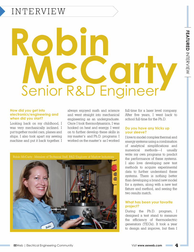
RobinMcCarty
Robin McCarty - Member of Technical Staff, R&D Engineer at Marlow Industries

EEWeb | Electrical Engineering Community Visit www.eeweb.com 5
INTERVIEWFEA
TURED IN
TERVIEW
used it for years to take data. When Marlow hired me, they asked me to design a similar but enhanced fixture. It was a great opportunity to start fresh and incorporate all of the new ideas I had.
What are you currently working on?We are targeting higher temperature energy harvesting applications. I think this is a niche for thermoelectric generators (TEG) where other energy harvesting technology can’t compete. In order to move our technology to higher temperatures, we have to target higher temperature materials, new device structures and fabrication methods, new test fixtures and new models. My focus is on the next generation TEG models and test fixtures.
Can you tell us more about Marlow Industries?Marlow was founded in 1973. The core business has been thermoelectric coolers and systems, but in recent years thermoelectric power generation has emerged. A thermoelectric cooler (TEC) uses current input and produces heat pumping while a thermoelectric generator (TEG) takes a temperature difference and produces current. Marlow is the premier supplier of TECs, TEGs and systems. We are also among the world leaders in developing TE materials, technologies and new products.
How did the idea of EverGen come about? Until a year ago, the existing thermoelectric technology that
was used in energy harvesting applications for low-power wireless sensors used thin-film thermoelectric materials. Because most energy harvesting applications will use a passive natural convection heat sink, a bulk thermoelectric material and device is a better thermal and mechanical match for these bulky, high thermal resistance heat sinks. Bottom line, I knew our devices would outperform the competition.
With the introduction of the low voltage DC-DC converters, our low electrical resistance, low cost, and high volume thermoelectric generators could be used for energy harvesting.
Marlow will continue to expand our thermoelectric
technology into new and emerging markets for both
cooling and power generation.
What are the goals of this project? Produce more power and start working at lower temperature differences than the competition. Throughout the project, we investigated what makes an optimal thermoelectric energy harvesting
system. Depending on the DC-DC converter technology used, the optimal TEG design (based on pure math and science) can be very similar to Marlow’s high volume, low cost thermoelectric coolers. It was a natural extension to use these types of TE devices for low cost, optimal thermal energy harvesting applications enabling Marlow to provide a cost effective thermal power source to replace batteries for wireless sensors.
How is this energy source able to power wireless sensors for the lifetime of the harvester?The EverGen series takes advantage of small, naturally occurring temperature differences that our customers encounter every day and converts it into small, sustaining power sources. The unique quality of our products is that it starts to produce power with as little as a 2°C temperature difference, much less than the current competition. This opens up a wide variety of applications such as providing power for sensors and actuators incorporated into smart buildings. With a perpetual power source, our customers do not need to worry about replacing batteries or other maintenance. The TEGs operating in their typical temperature ranges will be very reliable and virtually maintenance-free. Marlow leverages its long history producing extremely high reliability products for defense, space, telecommunications, medical and automotive applications.
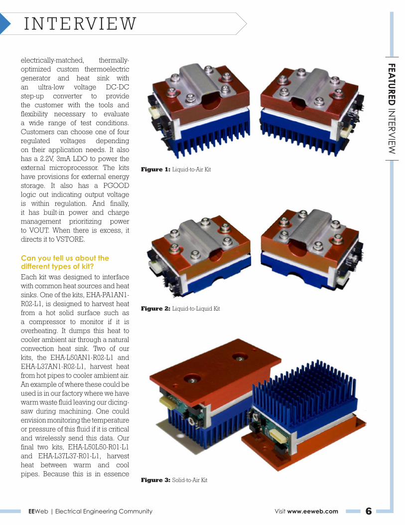
What does the EverGen series kit offer? Each system integrates a Marlow
EEWeb | Electrical Engineering Community Visit www.eeweb.com 6
INTERVIEWFEA
TURED IN
TERVIEW
electrically-matched, thermally-optimized custom thermoelectric generator and heat sink with an ultra-low voltage DC-DC step-up converter to provide the customer with the tools and flexibility necessary to evaluate a wide range of test conditions. Customers can choose one of four regulated voltages depending on their application needs. It also has a 2.2V, 3mA LDO to power the external microprocessor. The kits have provisions for external energy storage. It also has a PGOOD logic out indicating output voltage is within regulation. And finally, it has built-in power and charge management prioritizing power to VOUT. When there is excess, it directs it to VSTORE.
Can you tell us about the different types of kit? Each kit was designed to interface with common heat sources and heat sinks. One of the kits, EHA-PA1AN1-R02-L1, is designed to harvest heat from a hot solid surface such as a compressor to monitor if it is overheating. It dumps this heat to cooler ambient air through a natural convection heat sink. Two of our kits, the EHA-L50AN1-R02-L1 and EHA-L37AN1-R02-L1, harvest heat from hot pipes to cooler ambient air. An example of where these could be used is in our factory where we have warm waste fluid leaving our dicing-saw during machining. One could envision monitoring the temperature or pressure of this fluid if it is critical and wirelessly send this data. Our final two kits, EHA-L50L50-R01-L1 and EHA-L37L37-R01-L1, harvest heat between warm and cool pipes. Because this is in essence
Figure 1: Liquid-to-Air Kit
Figure 2: Liquid-to-Liquid Kit
Figure 3: Solid-to-Air Kit
EEWeb | Electrical Engineering Community Visit www.eeweb.com 7
INTERVIEWFEA
TURED IN
TERVIEW
a water-to-water heat exchanger, the thermal resistance is quite low and we are able to pull much more heat through the TEG, therefore producing more power at lower temperature differences. These devices could be used wherever the customer has a warm and cold water pipe in near proximity to each other, such as the water pipes going to any commercial sink.
What are some benefits that the customers will see using this technology?Customers will be able to produce small amounts of maintenance-free power wherever they have small temperature differences. By using EverGen products, our customers will see more power at smaller temperature differences, opening up a variety of applications previously not possible.
Where do you hope to see this technology implemented?Because our bulk thermoelectric technology is so scalable, we can scale up our liquid-to-air harvester to address remote sensing applications for applications such
as oil and gas monitoring that require Watts of power generation, multiple TEGs and heat sinks. This technology can be used as a stand-alone power source or work with other energy harvesting technologies.
What direction do you see your business heading in the next few years? Marlow will continue to expand our thermoelectric technology into new and emerging markets for both cooling and power generation. For energy harvesting, we will be targeting higher power systems ranging from hundreds of microwatts to multiple Watts and pushing our technology to higher operating temperatures.
What can we expect to see from Marlow Industries in the near future? EverGen (liquid-to-air systems) will be expanding to higher power output (multiple Watts) and higher temperature harvesting (up to 500°C) for process plants and oil and gas sensing. These assemblies will utilize very similar TEG and
converter technology but will be “super-sized” to include multiple TEGs and larger natural convection heat sink areas to accommodate pipes up to 12 inches in diameter.
What challenges do you foresee in our industry?Most customers will need a custom thermoelectric solution to maximize the power or efficiency of their systems. Thermoelectrics require specialized expertise to successfully incorporate them into systems. Educating our customers that these TEGs need to be electrically and thermally optimized for their systems is difficult. Most electrica engineers understand electrical matching but don’t appreciate thermal design; and most mechanical engineers understand thermal design but might not understand electrical matching. How do we create standardized solutions that engineers from diverse backgrounds can easily implement? ■
EEWebElectrical Engineering Community
Join Todaywww.eeweb.com/register

Avago Technologies new AEAT-6600 Hall E� ect Magnetic Encoder delivers optimal solutions for Robotic, Industrial and Medical systems designers.
• World’s highest resolution
• 16-bit absolute positiion through SSI
• Programmable Magnetic Rotary Encoder IC
• 16-pin TSSOP package
• Power down mode
New Encoder for the Worst Case Environments
Avago Technologies Motion Control Products
For more information and to requesta free sample go to: www.avagotech.com/motioncontrol

EEWeb | Electrical Engineering Community Visit www.eeweb.com 9
ICsTiming
Elie AyacheTiming Products
Keep Beat with Needs ofToday’s Embedded Market
Timing devices represent a substantial, steadily growing multi billion-dollar
market that encompasses both clock generator and buffer ICs, as well as frequency control devices. The large size of the timing market is not surprising if you consider that virtually all electronic devices contain a timing IC. Given the importance of timing products to the electronics industry, it’s surprising how slowly timing technology has evolved in recent years. In fact, over the past two decades, timing device suppliers have delivered clocking and frequency control products with a surprisingly slow rate of innovation. However, recent trends in the embedded market and the entry of new suppliers in that segment are driving innovation in timing technology that will
help designers improve system performance, simplify their designs and decrease their reliance on timing devices with historically long lead times.
A Snapshot of Timing Devices in Embedded Applications
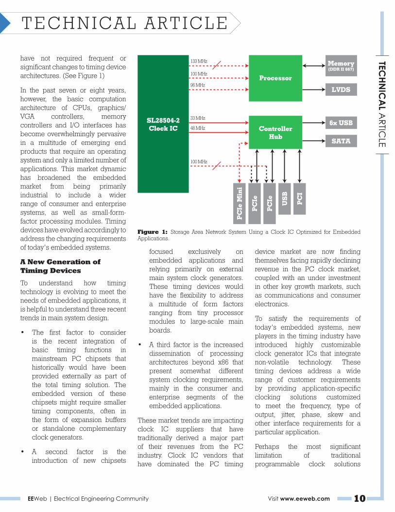
Classic embedded designs historically have focused on such applications as network and storage systems, industrial automation and controls, point of sale (POS) systems, test and measurement equipment, home and building automation, and medical systems. (See Figure 1 for an example of a clock IC used in a storage application with PCI-Express connectivity.) Mainstream x86 PC chipsets, or slightly modified versions of
these chipsets, are generally used in embedded applications. To meet the requirements of embedded systems, x86 chipsets have to achieve industrial grade compliance, and they typically have life spans of more than six years. If legacy chipset architectures required modifications to the main system clock, the changes would be infrequent and relatively minor, and it often made sense to accommodate these clock changes by adding discrete components to the board. To a great degree, this trend has kept the timing requirements of embedded systems very similar to their mainstream PC predecessors. Differences were mainly associated with the longer production life spans of certain products and their conformity to industrial grades. In short, embedded systems
EEWeb | Electrical Engineering Community Visit www.eeweb.com 10
TECHN
ICA
L ARTIC
LETECHNICAL ARTICLE
have not required frequent or significant changes to timing device architectures. (See Figure 1)
In the past seven or eight years, however, the basic computation architecture of CPUs, graphics/VGA controllers, memory controllers and I/O interfaces has become overwhelmingly pervasive in a multitude of emerging end products that require an operating system and only a limited number of applications. This market dynamic has broadened the embedded market from being primarily industrial to include a wider range of consumer and enterprise systems, as well as small-form-factor processing modules. Timing devices have evolved accordingly to address the changing requirements of today’s embedded systems.
A New Generation of Timing Devices
To understand how timing technology is evolving to meet the needs of embedded applications, it is helpful to understand three recent trends in main system design.
• The first factor to consider is the recent integration of basic timing functions in mainstream PC chipsets that historically would have been provided externally as part of the total timing solution. The embedded version of these chipsets might require smaller timing components, often in the form of expansion buffers or standalone complementary clock generators.
• A second factor is the introduction of new chipsets
focused exclusively on embedded applications and relying primarily on external main system clock generators. These timing devices would have the flexibility to address a multitude of form factors ranging from tiny processor modules to large-scale main boards.
• A third factor is the increased dissemination of processing architectures beyond x86 that present somewhat different system clocking requirements, mainly in the consumer and enterprise segments of the embedded applications.
These market trends are impacting clock IC suppliers that have traditionally derived a major part of their revenues from the PC industry. Clock IC vendors that have dominated the PC timing
device market are now finding themselves facing rapidly declining revenue in the PC clock market, coupled with an under investment in other key growth markets, such as communications and consumer electronics.
To satisfy the requirements of today’s embedded systems, new players in the timing industry have introduced highly customizable clock generator ICs that integrate non-volatile technology. These timing devices address a wide range of customer requirements by providing application-specific clocking solutions customized to meet the frequency, type of output, jitter, phase, skew and other interface requirements for a particular application.
Perhaps the most significant limitation of traditional programmable clock solutions
133 MHz
100 MHz
96 MHz
33 MHz
48 MHz
100 MHz
PC
Ie M
ini
PC
Ie
PC
Ie US
B
PC
I
SATA
SL28504-2Clock IC Controller
Hub
Processor
6x USB
LVDS
Memory(DDR II 667)
Figure 1: Storage Area Network System Using a Clock IC Optimized for Embedded Applications.
EEWeb | Electrical Engineering Community Visit www.eeweb.com 11
TECHN
ICA
L ARTIC
LETECHNICAL ARTICLE
is that they require I2C-based firmware or BIOS development. In many applications, an I2C interface is either not available or not desirable. New generations of configurable timing devices are now available to address the deficiencies associated with traditional I2C programmability solutions. These new timing products can be customized entirely at the factory or by using Web-based utilities. This customizable approach benefits the system design by alleviating the burden of using BIOS memory space and allocation of scarce firmware resources, as well as by assisting in boot time reduction. Once the device is customized, I2C programming may still be used for post-boot features such as hot swapping where the clock would need to be enabled on the fly at detection of a hardware card plug-in.
Another emerging trend in timing device technology is to provide flexibility in frequency generation and tuning capabilities of the clock signals. This latter capability has recently become important to developers due to the increased dissemination of differential signaling in embedded applications. In addition, the ability to provide features to help embedded designers minimize power consumption for mobile applications and green initiatives as well as conformity with governmental regulations, such as FCC regulations in the United States, have become common requirements.
And finally, timing devices are now offered in a variety of package types
that were not available a decade ago. These packages—some as tiny as 1.2 mm x 1.4 mm—are now available to address varying requirements for small form factors and manufacturability in today’s embedded applications.
Using Clock ICs to Combat EMI
Clock generator and buffer ICs are now available with built-in features, such as programmable edge rates, programmable impedance, programmable skew and spread spectrum technology, that can be used to combat electromagnetic interference (EMI) in embedded applications. These features can also be used to reduce radio frequency interference (RFI) in applications where interference with 3G/4G radios must be optimized to
improve device operation.
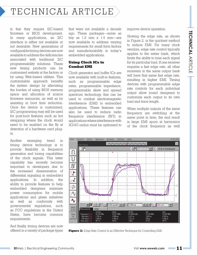
Slowing the edge rate, as shown in Figure 2, is the quickest method to reduce EMI. For many clock vendors, edge rate control typically applies to the entire bank, which limits the ability to tune each signal for its particular load. If one receiver requires a fast edge rate, all other receivers in the same output bank will have that same fast edge rate, resulting in higher EMI. Timing devices with programmable edge rate controls for each individual output allow board designers to customize each output to its own load and trace length.
When multiple outputs of the same frequency are switching at the same point in time, the end result is large EMI spurs at harmonics of the clock frequency as well
More(2 of 2)
File Control Setup Measure Analyze Utilities Help
T
3
8.00 GSa/s
10:53 AM
ClearAll
HH 5.00 ns/div TT 800 mV7.750 ns
On
0
500 mV/div (3 & 4 Combined)
ScalesMeasurements
Frequency (3•)Rise time (3•)Fall time (3•)
Duty cycle (3•)
current33.192 MHz1.736 ns1.268 ns48.7 %
mean33.271 MHz2.390 ms1.945 ns48.4%
std dev81.92034 kHz1.417 ns1.211 ns1.03%
min33.192 MHz1.029 ns720 ps47.2%
max33.356 MHz4.323 ns3.458 ns49.7%
3 4On
1
Figure 2: Edge Rate Control Is an Effective Technique for Controlling EMI.

EEWeb | Electrical Engineering Community Visit www.eeweb.com 12
TECHN
ICA
L ARTIC
LETECHNICAL ARTICLE
as increased noise at the power supplies due to the combined amount of switching current. By programming each clock output skew to be delayed relative to other outputs, the spur energy is spread out, which reduces peak EMI and power supply switching noise.
Most of today’s embedded systems implement differential clocking approaches for higher bandwidth; many board designers neglect the effects that these signal formats can have on EMI and system performance. Mismatch in the edge slew rate and skew between true and complement signals will
create common mode energy that radiates EMI, as well as an unstable cross-point that causes data loss. Because clock trees in these systems commonly drive multiple buses with differential outputs, any differential clock misalignments can generate a large amount of common mode energy. By using the I2C-programmable or factory-configurable skew and edge rate features, each I/O can be individually tuned to the PCB environment for cross-point optimization and EMI reduction.
Programmable impedance also allows board designers to
optimally match load impedance without having to modify discrete termination networks or PCB trace design. Mismatched trace impedance causes reflections that generate clock overshoot and undershoot, resulting in increased EMI and glitches in the clock circuitry of the receiving device.
Time for Mass Customization
Frequency customization has become a given, but what about addressing other parameters that developers care about when designing their systems and meeting their milestones, such as signal optimization or end product compliance with federal regulatory requirements? It’s still hard to convince system designers that there is such a thing as “mass” customization in timing, enabling the best-fit timing solution regardless of the application without months of lead times or a lot of non-recurring engineering (NRE) expenses.
Now that embedded designs have expanded beyond classic industrial systems and have migrated into faster-paced consumer and enterprise markets, there is a greater sense of urgency to get products to market quickly. Today’s timing device suppliers must be able to respond quickly to the developer’s customization needs. Until recently, custom configurations were achieved through changes in the IC design, layout, masks and new wafer developments. This customization process often required lengthy lead times of three to four months to deliver working products to the customer.
Silicon Labs > Products > Clocks & Oscillators > ClockBuilder
ClockBuilder™ UtilityStep 1: Specify Requirements > Step 2: Preview Configuration > Step 3: Initiate Request
Home | About Us | News | Investor Relations
• Products • Applications • Support • Buy or Sample
Oscillator
ControlLogic
PLL
CLK0
CLK1
CLK2
XA
XB
Vc
P0
VCXO
Specify your custom clock by selecting parameters below. Need help? View the ClockBuilder video tutorial.
Input Type: Crystal + VCX
Crystal VC
Package: 10-MSOP
Output Frequency: 0.008 to 133 MHz
Modulation: Down Spread
Modulation Rate: 31.5 kHz
The Si5350 has programmable input pins that can be factory-customized to support any of the following functions.
You may choose up to 1 optional control pin functions:
Any Si5350 output clock can be connected to either the crystal or the analog control voltage input.
Any OE pin can be mapped to control any output clock. Use the table below to assign OE control to specificoutput clocks. The device pinout will be assigned based on the selected frequency configuration.
Crystal Frequency: 27 MHz
Internal LoadCapacitance (CL):
VCXO Pull Range:
Block Diagram
Si5350B
Input
Optional Control Pins
Output Clocks
Output Enable (OEB) Pins: 0
Powerdown (PDN) Pins: 0
Spread SpectrumClocking (SSC): Disabled
Percentage: (-0.1% to -2.5%)1.0
10 pf
+/- 120ppm
MultiSynth
0
MultiSynth
1
MultiSynth
2
OutputFrequency
(MHz) OE Control Pin ReferenceEnable
SSCEnable
Channel
Crystal VC
Crystal VC
Figure 3: Web-Based Utilities Enable Rapid Customization of Timing Devices.
EEWeb | Electrical Engineering Community Visit www.eeweb.com 13
TECHN
ICA
L ARTIC
LETECHNICAL ARTICLE
Factory and web-customization of timing devices represents a significant advantage by enabling the embedded developer to avoid having to develop BIOS subroutines for the sole purpose of configuring the clock. The developer gets an added bonus of receiving clock samples in a couple of weeks instead of months—60 percent faster than mask-customized clocks.
Perhaps the most significant benefit to embedded developers provided by web-customized, programmable timing devices is that they are no longer only available for the highest volume applications. Using web-based clock configuration utilities such as Silicon Labs’ ClockBuilder (shown in Figure 3),
embedded designers can now expect platform-specific timing solutions with lead times as short as two weeks regardless of the size of their project. Now, anyone with an Internet connection can configure timing devices online and enjoy the benefits of having fully customized, application-specific clocks and oscillators with lead times as short as two weeks.
About the Author
Elie Ayache manages Silicon Labs’ high-volume clock IC business. Offering more than 20 years of experience in the timing industry, Mr. Ayache joined Silicon Labs in 2011 following the company’s acquisition of SpectraLinear,
where he served as vice president of marketing. Previously, he was the marketing director of the computation clock business Unit at Cypress Semiconductor. Before joining Cypress, he served as director of marketing and applications engineering at IMI where he pioneered numerous launches of innovative products. Mr. Ayache also spent several years in the area of mixed-signal ASIC design where he patented the linear frequency shift doze mode for green applications as well as the power-up bidirectional I/O, which are still widely used in the industry today. Mr. Ayache has a BSEE degree from Santa Clara University. ■
BeStar®
ACOUSTICS & SENSORS
Teamwork • Technology • Invention • Listen • Hear
PRODUCTSSpeakers
Buzzers
Piezo Elements
Back-up Alarms
Horns
Sirens/Bells
Beacons
Microphones
Sensors
INDUSTRIESAutomotive
Durables
Medical
Industrial
Mobile
Fire / Safety
Security
Consumer
Leisure
QS9000 • TS/ ISO16949 • ISO14001 • ISO13485 • ISO9001
bestartech.com | [email protected] | 520.439.9204
Preferred acoustic componentsupplier to OEMs worldwide
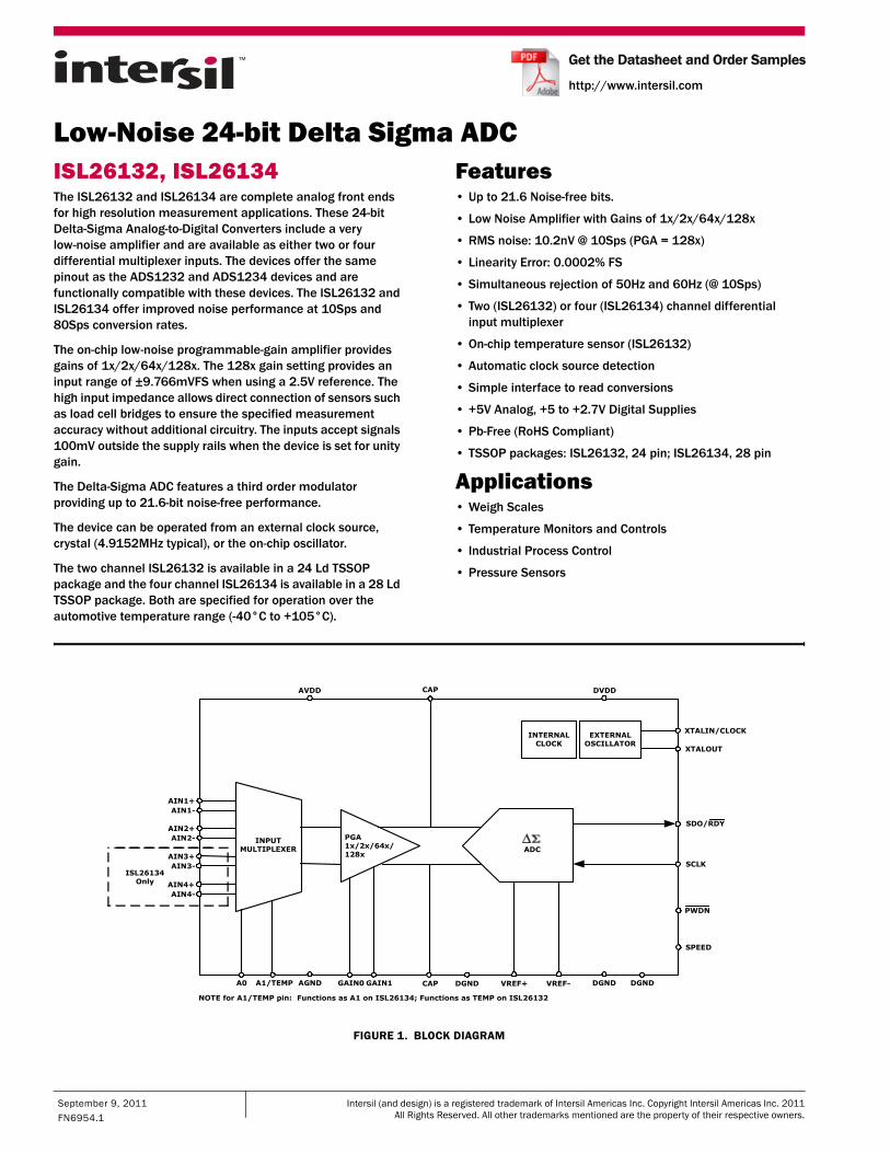
Low-Noise 24-bit Delta Sigma ADCISL26132, ISL26134The ISL26132 and ISL26134 are complete analog front ends for high resolution measurement applications. These 24-bit Delta-Sigma Analog-to-Digital Converters include a very low-noise amplifier and are available as either two or four differential multiplexer inputs. The devices offer the same pinout as the ADS1232 and ADS1234 devices and are functionally compatible with these devices. The ISL26132 and ISL26134 offer improved noise performance at 10Sps and 80Sps conversion rates.
The on-chip low-noise programmable-gain amplifier provides gains of 1x/2x/64x/128x. The 128x gain setting provides an input range of ±9.766mVFS when using a 2.5V reference. The high input impedance allows direct connection of sensors such as load cell bridges to ensure the specified measurement accuracy without additional circuitry. The inputs accept signals 100mV outside the supply rails when the device is set for unity gain.
The Delta-Sigma ADC features a third order modulator providing up to 21.6-bit noise-free performance.
The device can be operated from an external clock source, crystal (4.9152MHz typical), or the on-chip oscillator.
The two channel ISL26132 is available in a 24 Ld TSSOP package and the four channel ISL26134 is available in a 28 Ld TSSOP package. Both are specified for operation over the automotive temperature range (-40°C to +105°C).
Features• Up to 21.6 Noise-free bits.
• Low Noise Amplifier with Gains of 1x/2x/64x/128x
• RMS noise: 10.2nV @ 10Sps (PGA = 128x)
• Linearity Error: 0.0002% FS
• Simultaneous rejection of 50Hz and 60Hz (@ 10Sps)
• Two (ISL26132) or four (ISL26134) channel differential input multiplexer
• On-chip temperature sensor (ISL26132)
• Automatic clock source detection
• Simple interface to read conversions
• +5V Analog, +5 to +2.7V Digital Supplies
• Pb-Free (RoHS Compliant)
• TSSOP packages: ISL26132, 24 pin; ISL26134, 28 pin
Applications• Weigh Scales
• Temperature Monitors and Controls
• Industrial Process Control
• Pressure Sensors
ADC
PGA1x/2x/64x/128x
INTERNAL CLOCK
SDO/RDY
SCLK
DVDDAVDD
DGNDAGND
XTALIN/CLOCK
VREF+
EXTERNAL OSCILLATOR
XTALOUT
VREF-A0 A1/TEMP
AIN1+AIN1-
AIN2+AIN2-
AIN3+AIN3-
AIN4+AIN4-
INPUTMULTIPLEXER
ISL26134 Only
CAP
CAP
GAIN1GAIN0
PWDN
SPEED
DGNDDGND
NOTE for A1/TEMP pin: Functions as A1 on ISL26134; Functions as TEMP on ISL26132
FIGURE 1. BLOCK DIAGRAM
September 9, 2011FN6954.1
Get the Datasheet and Order Samples
http://www.intersil.com
Intersil (and design) is a registered trademark of Intersil Americas Inc. Copyright Intersil Americas Inc. 2011All Rights Reserved. All other trademarks mentioned are the property of their respective owners.
EEWeb | Electrical Engineering Community Visit www.eeweb.com 15
EnergyMillimeter Scale
HarvestingBased Sensors
Steve GradyVP Marketing
This article introduces several new concepts for creating millimeter scale intelligent sensors using ambient energy harvesting to power the device
autonomously. Using the energy surrounding the sensor can provide life-of-product powering. Energy harvesting techniques are used in large scale applications like solar panel installations and wind farms. But energy harvesting can also be used in extremely small scale devices as is demonstrated in this article. Light is converted to electricity, stored in rechargeable solid state batteries and delivered to the sensor system. There are no traditional batteries to change out and devices can be placed anywhere.
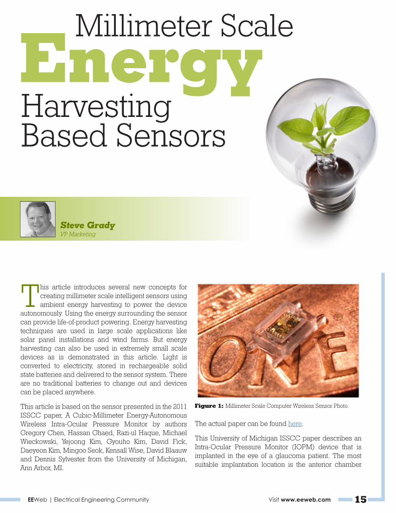
This article is based on the sensor presented in the 2011 ISSCC paper, A Cubic-Millimeter Energy-Autonomous Wireless Intra-Ocular Pressure Monitor by authors Gregory Chen, Hassan Ghaed, Razi-ul Haque, Michael Wieckowski, Yejoong Kim, Gyouho Kim, David Fick, Daeyeon Kim, Mingoo Seok, Kensall Wise, David Blaauw and Dennis Sylvester from the University of Michigan, Ann Arbor, MI.
Figure 1: Millimeter Scale Computer Wireless Sensor Photo.
The actual paper can be found here.
This University of Michigan ISSCC paper describes an Intra-Ocular Pressure Monitor (IOPM) device that is implanted in the eye of a glaucoma patient. The most suitable implantation location is the anterior chamber
EEWeb | Electrical Engineering Community Visit www.eeweb.com 16
TECHN
ICA
L ARTIC
LETECHNICAL ARTICLE
of the eye, which is surgically accessible and out of the field of vision. The IOPM volume is limited to 1.5 cubic millimeters. This aggressive IOPM size constraint creates major challenges for achieving high-resolution capacitance measurements, wireless communication, and multi-year device lifetime. Little energy can be stored on the tiny IOPM system, calling for ultra-low power operation and energy harvesting. The required millimeter antennas or inductors result in lower received power and higher transmission frequency, both increasing micro-system power. The IOPM harvests solar energy that enters the eye through the transparent cornea to achieve energy autonomy. The IOPM contains an integrated solar cell, EnerChip™ thin-film Li battery, MEMS capacitive sensor, and integrated circuits vertically assembled in a biocompatible glass housing as shown in Figure 1. The circuits include a wireless transceiver, capacitance to digital converter (CDC), DC-DC switched capacitor network (SCN), microcontroller (μP), and memory fabricated in 0.18μm CMOS.
Why Millimeter Scale?
As in the case of the Intra-Ocular Pressure Monitor, it is often desirable to place microelectronic systems in very small spaces. New advances in ultra-low power Integrated Circuits, MEMS sensors and Solid State Batteries are making these systems a reality. Miniature wireless sensors, data loggers and computers can now be embedded in hundreds of new applications and millions of locations.
Ultra-Low Power Management is Key
The desired IOPM lifetime is years to converge on a suitable glaucoma treatment. However, the anterior chamber volume limits lifetime by constraining the size and capacity of the micro-system’s power sources. The IOPM uses a 1μAh EnerChip™ solid state battery from Cymbet. The lifetime is 28 days with no energy harvesting!
To extend lifetime, the IOPM harvests light energy entering the eye with an integrated 0.07 square millimeter solar cell that recharges the battery. Given the ultra-small solar cell size, energy autonomy requires average power consumption of less than 10nW. For the majority of its lifetime, the IOPM is in a 3.65nW standby mode where mixed-signal circuits are disabled, digital logic is power-gated, and 2.4fW/bitcell SRAM retains IOP instructions
and data. The average system power with pressure measurements every 15 minutes and daily wireless data transmissions is 5.3nW. When sunny, the solar cells supply 80.6nW to the battery. The combination of energy harvesting and low-power operation allows the IOPM to achieve zero-net energy operation in low light. The IOPM requires 10 hours of indoor lighting or 1.5 hours of sunlight per day to achieve energy-autonomy.
EH Wireless Sensor Components
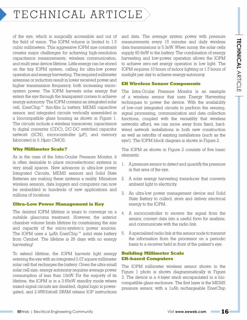
The Intra-Ocular Pressure Monitor is an example of a wireless sensor that uses Energy Harvesting techniques to power the device. With the availability of low-cost integrated circuits to perform the sensing, signal processing, communication and data collection functions, coupled with the versatility that wireless networks afford, we can move away from fixed, hard-wired network installations in both new construction as well as retrofits of existing installations (such as the eye!). The IOPM block diagram is shown in Figure 2.
The IOPM as shown in Figure 2 consists of five basic elements:
1. A pressure sensor to detect and quantify the pressure in that area of the eye.
2. A solar energy harvesting transducer that converts ambient light to electricity.
3. An ultra-low power management device and Solid State Battery to collect, store and deliver electrical energy to the IOPM.
4. A microcontroller to receive the signal from the sensor, convert data into a useful form for analysis, and communicate with the radio link.
5. A specialized radio link at the sensor node to transmit the information from the processor on a periodic basis to a receiver held in front of the patient’s eye.
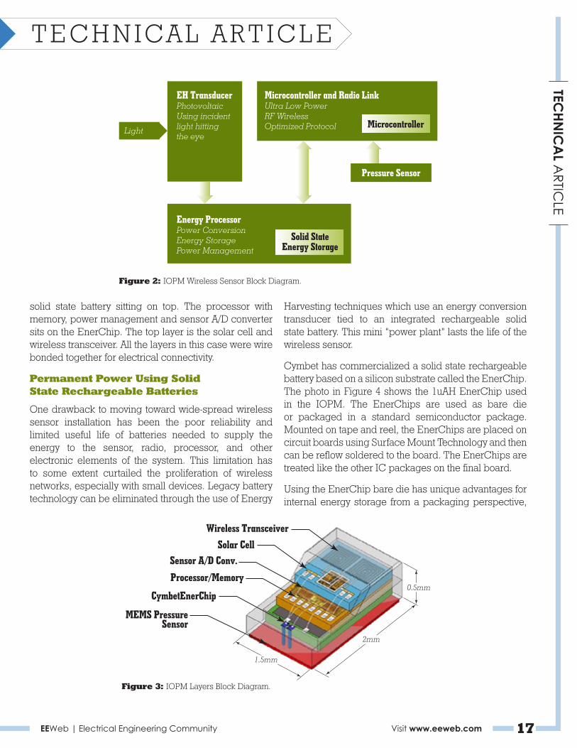
Building Millimeter Scale EH-based Computers
The IOPM millimeter wireless sensor shown in the Figure 1 photo is shown diagrammatically in Figure 3. The device is a 4-layer stack encapsulated in a bio-compatible glass enclosure. The first layer is the MEMS pressure sensor, with a 1uAh rechargeable EnerChip
EEWeb | Electrical Engineering Community Visit www.eeweb.com 17
TECHN
ICA
L ARTIC
LETECHNICAL ARTICLE
solid state battery sitting on top. The processor with memory, power management and sensor A/D converter sits on the EnerChip. The top layer is the solar cell and wireless transceiver. All the layers in this case were wire bonded together for electrical connectivity.
Permanent Power Using Solid State Rechargeable Batteries
One drawback to moving toward wide-spread wireless sensor installation has been the poor reliability and limited useful life of batteries needed to supply the energy to the sensor, radio, processor, and other electronic elements of the system. This limitation has to some extent curtailed the proliferation of wireless networks, especially with small devices. Legacy battery technology can be eliminated through the use of Energy
Figure 2: IOPM Wireless Sensor Block Diagram.
Harvesting techniques which use an energy conversion transducer tied to an integrated rechargeable solid state battery. This mini “power plant” lasts the life of the wireless sensor.
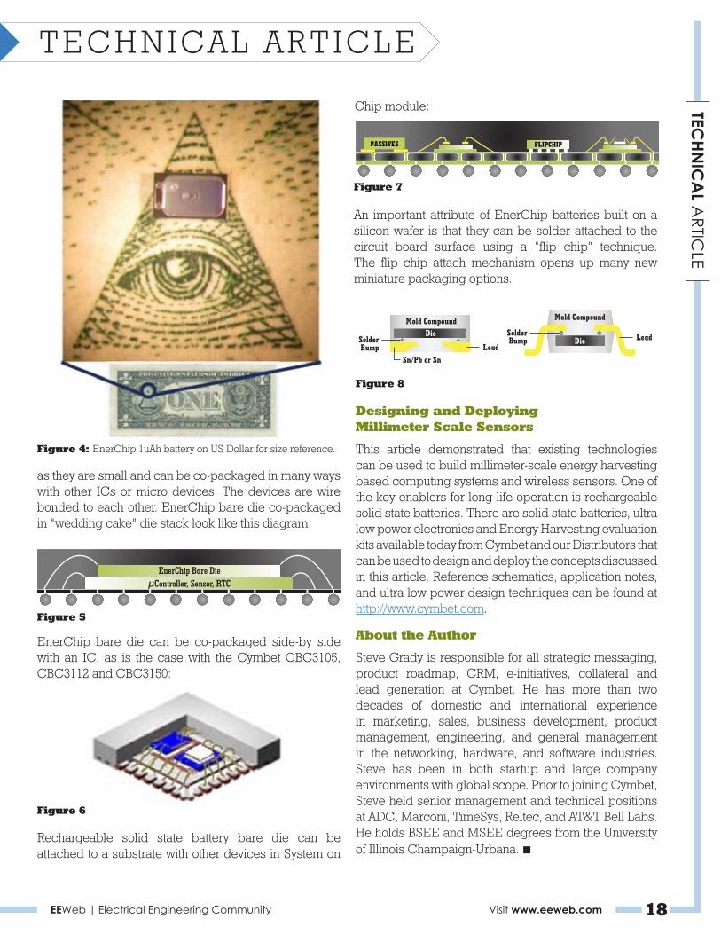
Cymbet has commercialized a solid state rechargeable battery based on a silicon substrate called the EnerChip. The photo in Figure 4 shows the 1uAH EnerChip used in the IOPM. The EnerChips are used as bare die or packaged in a standard semiconductor package. Mounted on tape and reel, the EnerChips are placed on circuit boards using Surface Mount Technology and then can be reflow soldered to the board. The EnerChips are treated like the other IC packages on the final board.
Using the EnerChip bare die has unique advantages for internal energy storage from a packaging perspective,
Figure 3: IOPM Layers Block Diagram.
EH TransducerPhotovoltaicUsing incidentlight hittingthe eye
Energy ProcessorPower ConversionEnergy StoragePower Management
Microcontroller and Radio LinkUltra Low PowerRF WirelessOptimized Protocol Microcontroller
Solid StateEnergy Storage
Pressure Sensor
Light
Wireless TransceiverSolar Cell
Sensor A/D Conv.Processor/Memory
CymbetEnerChip
MEMS PressureSensor
2mm
0.5mm
1.5mm
EEWeb | Electrical Engineering Community Visit www.eeweb.com 18
TECHN
ICA
L ARTIC
LETECHNICAL ARTICLE
as they are small and can be co-packaged in many ways with other ICs or micro devices. The devices are wire bonded to each other. EnerChip bare die co-packaged in “wedding cake” die stack look like this diagram:
Figure 4: EnerChip 1uAh battery on US Dollar for size reference.
EnerChip bare die can be co-packaged side-by side with an IC, as is the case with the Cymbet CBC3105, CBC3112 and CBC3150:
Figure 5
Figure 6
Chip module:
Figure 7
An important attribute of EnerChip batteries built on a silicon wafer is that they can be solder attached to the circuit board surface using a “flip chip” technique. The flip chip attach mechanism opens up many new miniature packaging options.
Figure 8
Designing and Deploying Millimeter Scale Sensors
This article demonstrated that existing technologies can be used to build millimeter-scale energy harvesting based computing systems and wireless sensors. One of the key enablers for long life operation is rechargeable solid state batteries. There are solid state batteries, ultra low power electronics and Energy Harvesting evaluation kits available today from Cymbet and our Distributors that can be used to design and deploy the concepts discussed in this article. Reference schematics, application notes, and ultra low power design techniques can be found at http://www.cymbet.com.
About the Author
Steve Grady is responsible for all strategic messaging, product roadmap, CRM, e-initiatives, collateral and lead generation at Cymbet. He has more than two decades of domestic and international experience in marketing, sales, business development, product management, engineering, and general management in the networking, hardware, and software industries. Steve has been in both startup and large company environments with global scope. Prior to joining Cymbet, Steve held senior management and technical positions at ADC, Marconi, TimeSys, Reltec, and AT&T Bell Labs. He holds BSEE and MSEE degrees from the University of Illinois Champaign-Urbana. ■
Rechargeable solid state battery bare die can be attached to a substrate with other devices in System on
EnerChip Bare DieµController, Sensor, RTC
FLIPCHIPPASSIVES
DieDie Lead
Mold CompoundMold Compound
LeadSn/Pb or Sn
SolderBump
SolderBump

1.800.574.2791
EEWeb
Contact Us For Advertising Opportunities
www.eeweb.com/advertising
Electrical Engineering Community

EEWeb | Electrical Engineering Community Visit www.eeweb.com 20
RETURN TO
ZERORETURN TO ZERO

EEWeb | Electrical Engineering Community Visit www.eeweb.com 21
RETURN TO
ZERORETURN TO ZERO
EEWebElectrical Engineering Community
Join Todaywww.eeweb.com/register