EELE 367 – Logic Design Module 1 – Classic Digital Design Agenda 1.Number Systems...
136
EELE 367 – Logic Design Module 1 – Classic Digital Design • Agenda 1. Number Systems 2. Combinational Logic 3. Sequential Logic
-
Upload
quentin-arnold -
Category
Documents
-
view
218 -
download
0
Transcript of EELE 367 – Logic Design Module 1 – Classic Digital Design Agenda 1.Number Systems...

EELE 367 – Logic Design
Module 1 – Classic Digital Design
• Agenda
1. Number Systems
2. Combinational Logic
3. Sequential Logic
Module 1: Classic Digital Design 2
Number Systems
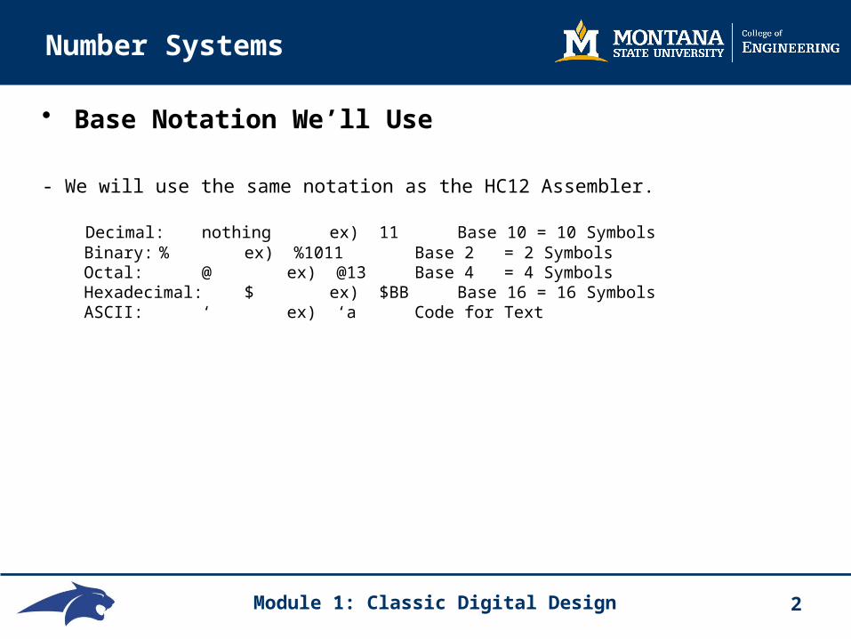
• Base Notation We’ll Use
- We will use the same notation as the HC12 Assembler.
Decimal: nothing ex) 11 Base 10 = 10 Symbols Binary: % ex) %1011 Base 2 = 2 Symbols Octal: @ ex) @13 Base 4 = 4 Symbols Hexadecimal: $ ex) $BB Base 16 = 16 Symbols ASCII: ‘ ex) ‘a Code for Text

Module 1: Classic Digital Design 3
Number Systems
• Base Conversion – Binary to Decimal
- each digit has a “weight” of 2n that depends on the position of the digit - multiply each digit by its “weight”
- sum the resultant products
ex) Convert %1011 to decimal
23 22 21 20 (weight)
%1 0 1 1
= 1•(23) + 0• (22) + 1• (21) + 1• (20) = 1•(8) + 0• (4) + 1• (2) + 1• (1)
= 8 + 0 + 2 + 1 = 11 Decimal

Module 1: Classic Digital Design 4
Number Systems
• Base Conversion – Binary to Decimal with Fractions
- the weight of the binary digits have negative positions
ex) Convert %1011.101 to decimal
23 22 21 20 2-1 2-2 2-3 %1 0 1 1 . 1 0 1
= 1•(23) + 0• (22) + 1• (21) + 1• (20) + 1• (2-1) + 0• (2-2) + 1• (2-
3)= 1•(8) + 0• (4) + 1• (2) + 1• (1) + 1• (0.5) + 0• (0.25) + 1•
(0.125) = 8 + 0 + 2 + 1 + 0.5 + 0 + 0.125
= 11.625 Decimal

Module 1: Classic Digital Design 5
Number Systems
• Base Conversion – Decimal to Binary
- the decimal number is divided by 2, the remainder is recorded - the quotient is then divided by 2, the remainder is recorded - the process is repeated until the quotient is zero
ex) Convert 11 decimal to binary
Quotient Remainder
2 11 5 1 LSB 2 5 2 1 2 2 1 0 2 1 0 1 MSB
= %1011
Module 1: Classic Digital Design 6
Number Systems
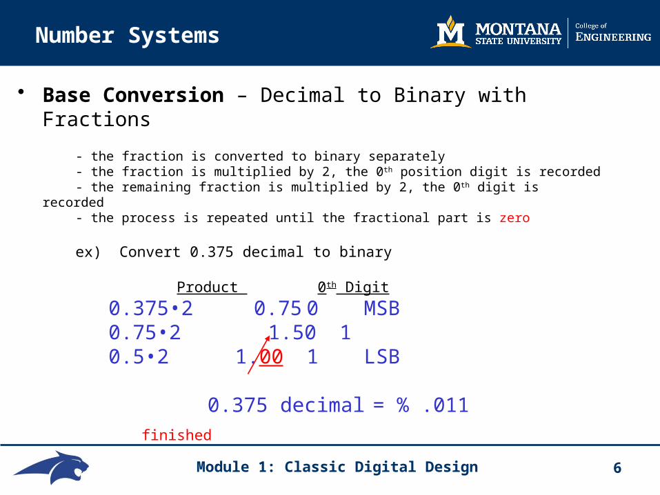
• Base Conversion – Decimal to Binary with Fractions
- the fraction is converted to binary separately - the fraction is multiplied by 2, the 0th position digit is recorded - the remaining fraction is multiplied by 2, the 0th digit is recorded - the process is repeated until the fractional part is zero
ex) Convert 0.375 decimal to binary
Product 0th Digit
0.375•2 0.75 0 MSB0.75•2 1.50 1 0.5•2 1.00 1 LSB
0.375 decimal = % .011
finished

Module 1: Classic Digital Design 7
Number Systems
• Base Conversion – Hex to Decimal
- the same process as “binary to decimal” except the weights are now BASE 16 - NOTE ($A=10, $B=11, $C=12, $D=13, $E=14, $F=15)
ex) Convert $2BC to decimal
162 161 160 (weight)
$2 B C
= 2• (162) + B• (161) + C• (160) = 2•(256) + 11• (16) + 12• (1)
= 512 + 176 + 12 = 700 Decimal
Module 1: Classic Digital Design 8
Number Systems
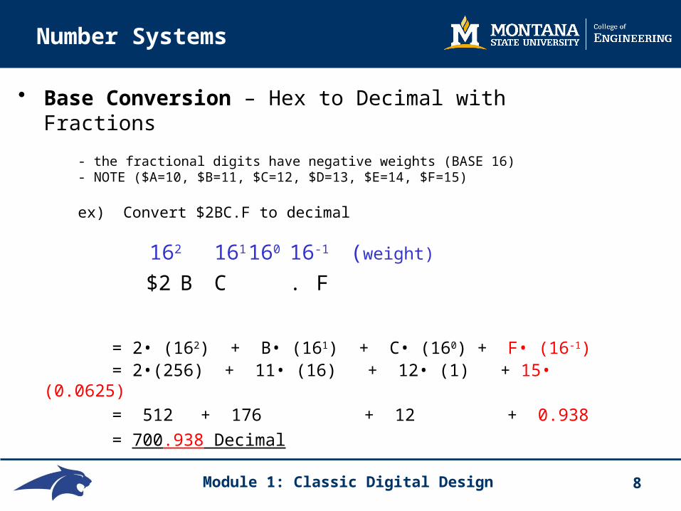
• Base Conversion – Hex to Decimal with Fractions
- the fractional digits have negative weights (BASE 16) - NOTE ($A=10, $B=11, $C=12, $D=13, $E=14, $F=15)
ex) Convert $2BC.F to decimal
162 161 160 16-1 (weight)
$2 B C . F
= 2• (162) + B• (161) + C• (160) + F• (16-1) = 2•(256) + 11• (16) + 12• (1) + 15• (0.0625)
= 512 + 176 + 12 + 0.938 = 700.938 Decimal

Module 1: Classic Digital Design 9
Number Systems
• Base Conversion – Decimal to Hex
- the same procedure is used as before but with BASE 16 as the divisor/multiplier ex) Convert 420.625 decimal to hex
1st, convert the integer part…
Quotient Remainder
16 420 26 4 LSB 16 26 1 10 16 1 0 1 MSB = $1A4
2nd, convert the fractional part…Product 0th Digit
0.625•16 10.00 10 MSB = $ .A
420.625 decimal = $1A4.A
Module 1: Classic Digital Design 10
Number Systems
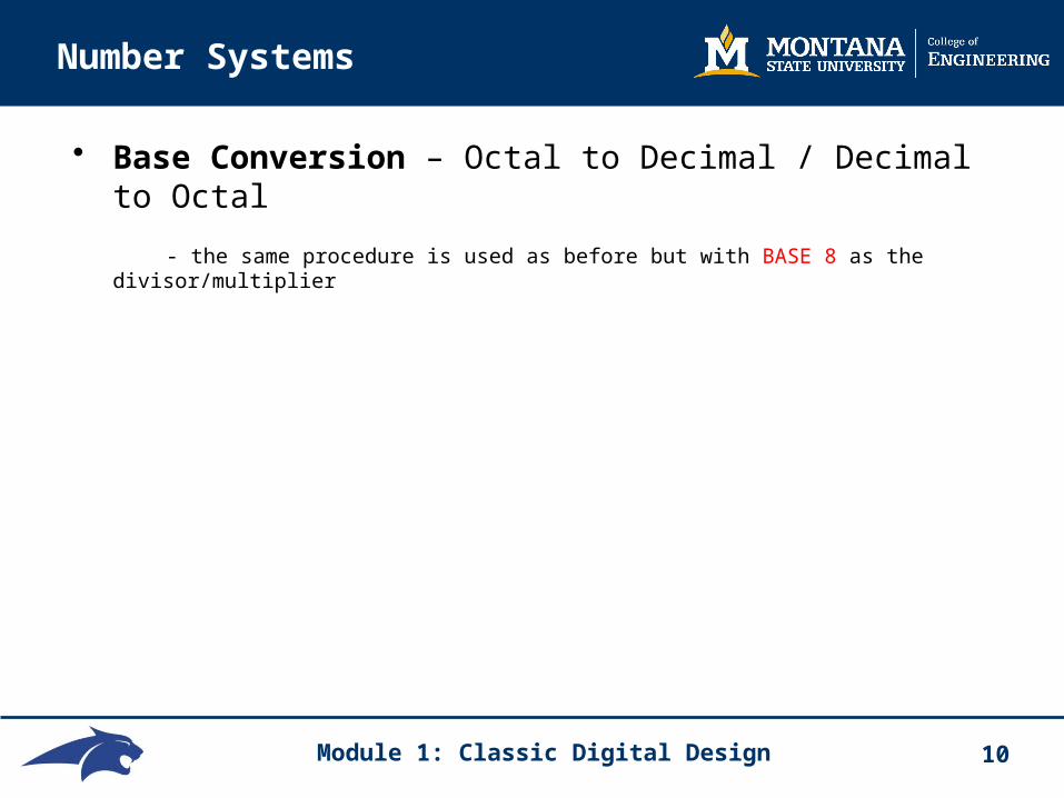
• Base Conversion – Octal to Decimal / Decimal to Octal - the same procedure is used as before but with BASE 8 as the divisor/multiplier

Module 1: Classic Digital Design 11
Number Systems
• Base Conversion – Hex to Binary
- each HEX digit is made up of four binary bits ex) Convert $ABC to binary
$A B C
= % 1010 1011 1100
= %1010 1011 1100
Module 1: Classic Digital Design 12
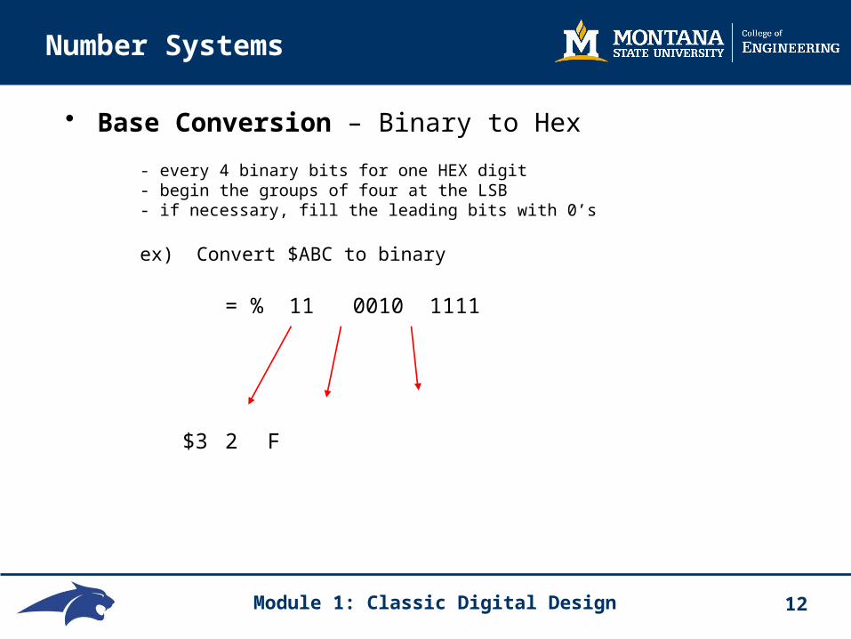
Number Systems
• Base Conversion – Binary to Hex
- every 4 binary bits for one HEX digit - begin the groups of four at the LSB - if necessary, fill the leading bits with 0’s ex) Convert $ABC to binary
= % 11 0010 1111
$3 2 F
Module 1: Classic Digital Design 13
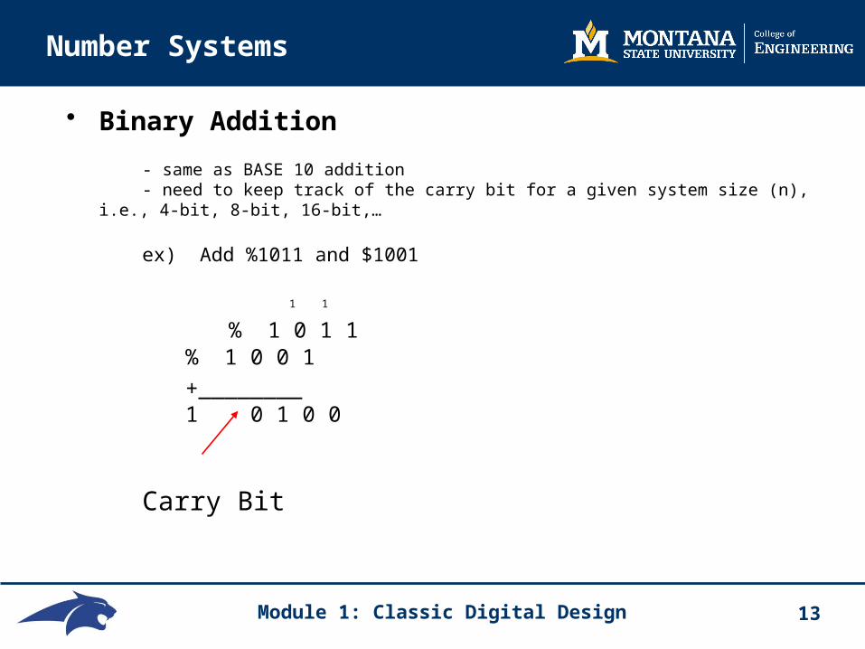
Number Systems
• Binary Addition
- same as BASE 10 addition - need to keep track of the carry bit for a given system size (n), i.e., 4-bit, 8-bit, 16-bit,… ex) Add %1011 and $1001
1 1
% 1 0 1 1% 1 0 0 1
+________ 1 0 1 0 0
Carry Bit
Module 1: Classic Digital Design 14
Number Systems
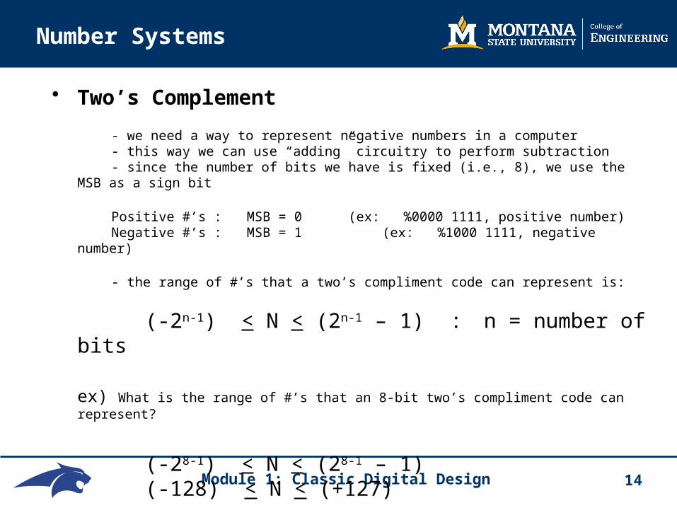
• Two’s Complement
- we need a way to represent negative numbers in a computer - this way we can use “adding” circuitry to perform subtraction - since the number of bits we have is fixed (i.e., 8), we use the MSB as a sign bit
Positive #’s : MSB = 0 (ex: %0000 1111, positive number) Negative #’s : MSB = 1 (ex: %1000 1111, negative number) - the range of #’s that a two’s compliment code can represent is:
(-2n-1) < N < (2n-1 – 1) : n = number of bits
ex) What is the range of #’s that an 8-bit two’s compliment code can represent?
(-28-1) < N < (28-1 – 1) (-128) < N < (+127)

Module 1: Classic Digital Design 15
Number Systems
• Two’s Complement Negation
- to take the two’s compliment of a positive number (i.e., find its negative equivalent)
Nc = 2n – N Nc = Two’s Compliment N = Original Positive Number
ex) Find the 8-bit two’s compliment representation of –52dec
N = +52dec
Nc = 28 – 52 = 256 – 52 = 204 = %1100 1100
Note the Sign Bit

Module 1: Classic Digital Design 16
Number Systems
• Two’s Complement Negation (a second method)
- to take the two’s compliment of a positive number (i.e., find its negative equivalent)
1) Invert all the bits of the original positive number (binary) 2) Add 1 to the result
ex) Find the 8-bit two’s compliment representation of –52dec
N = +52dec = %0011 0100
Invert: = %1100 1011 Add 1 = %1100 1011 + 1 -------------------- %1100 1100 (-52dec)

Module 1: Classic Digital Design 17
Number Systems
• Two’s Complement Addition - Addition of two’s compliment numbers is performed just like standard binary addition - However, the carry bit is ignored
Module 1: Classic Digital Design 18
Number Systems
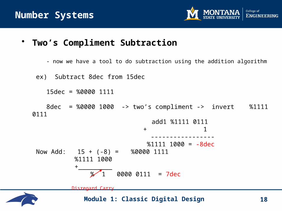
• Two’s Compliment Subtraction
- now we have a tool to do subtraction using the addition algorithm
ex) Subtract 8dec from 15dec
15dec = %0000 1111 8dec = %0000 1000 -> two’s compliment -> invert %1111 0111 add1 %1111 0111 + 1 ----------------- %1111 1000 = -8dec Now Add: 15 + (-8) = %0000 1111 %1111 1000 +_________ % 1 0000 0111 = 7dec
Disregard Carry

Module 1: Classic Digital Design 19
Number Systems
• Two’s Compliment Overflow
- If a two’s compliment subtraction results in a number that is outside the range of representation (i.e., -128 < N < +127), an “overflow” has occurred.
ex) -100dec – 100dec- = -200dec (can’t represent)
- There are three cases when overflow occurs
1) Sum of like signs results in answer with opposite sign 2) Negative – Positive = Positive 3) Positive – Negative = Negative
- Boolean logic can be used to detect these situations.

Module 1: Classic Digital Design 20
Number Systems
• Binary Coded Decimal
- Sometimes we wish to represent an individual decimal digit as a binary representation (i.e., 7-segment display to eliminate a decoder)
- We do this by using 4 binary digits.
Decimal BCD 0 0000 1 0001 ex) Represent 17dec 2 0010 3 0011 Binary = %10111 4 0100 BCD = %0001 0111 5 0101 6 0110 7 0111 8 1000 9 1001

Module 1: Classic Digital Design 21
Number Systems
• ASCII
- American Standard Code for Information Interchange - English Alphanumeric characters are represented with a 7-bit code
ex) ‘A’ = $40
‘a’ = $61

Module 1: Classic Digital Design 22
Number Systems
• Important Things to Remember
Know the Code :
A computer just knows 1’s and 0’s. It is up to you to keep trace of whether the bits represent unsigned numbers, two’s complement, ASCII, etc…
Two’s Complement Size :
2’s Complement always need a “size” associated with it. We always say “n-bit, two’s complement”
Module 1: Classic Digital Design 23
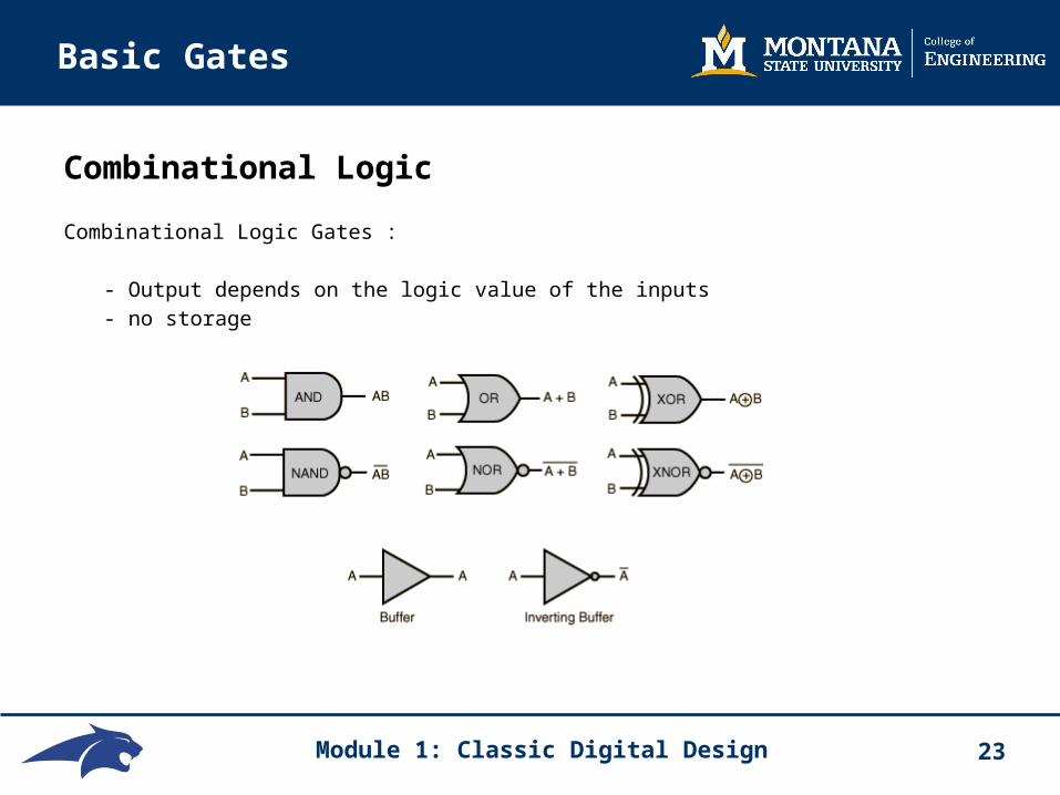
Combinational Logic
Combinational Logic Gates :
- Output depends on the logic value of the inputs
- no storage
Basic Gates
Module 1: Classic Digital Design 24
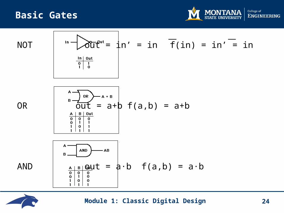
NOT out = in’ = in f(in) = in’ = in
OR out = a+b f(a,b) = a+b
AND out = a·b f(a,b) = a·b
Basic Gates

Module 1: Classic Digital Design 25
XOR out = ab f(a,b) = ab
NOR out = a+b f(a,b) = a+b
NAND out = a·b f(a,b) = a·b
Basic Gates
Module 1: Classic Digital Design 26
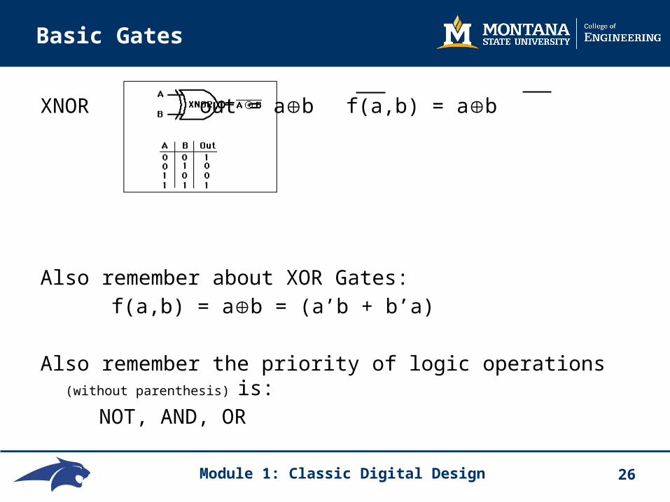
XNOR out = ab f(a,b) = ab
Also remember about XOR Gates:
f(a,b) = ab = (a’b + b’a)
Also remember the priority of logic operations (without parenthesis) is:
NOT, AND, OR
Basic Gates

Module 1: Classic Digital Design 27
Boolean Algebra
• Boolean Algebra- formulated by mathematician George Boole in 1854
- basic relationships & manipulations for a two-value system
• Switching Algebra- adaptation of Boolean Logic to analyzer and describe behavior of relays
- Claude Shannon of Bell Labs in 1938
- this works for all switches (mechanical or electrical)
- we generally use the terms "Boolean Algebra" & "Switching Algebra" interchangeably
Module 1: Classic Digital Design 28
Boolean Algebra
• What is Algebra- the basic set of rules that the elements and operators in a system follow
- the ability to represent unknowns using variables
- the set of theorems available to manipulate expressions
• Boolean- we limit our number set to two values (0, 1)
- we limit our operators to AND, OR, INV

Module 1: Classic Digital Design 29
Boolean Algebra
• Axioms- also called "Postulates"
- minimal set of basic definitions that we assume to be true
- all other derivations are based on these truths
- since we only have two values in our system, we typically define an axiom and then its complement (A1 & A1')

Module 1: Classic Digital Design 30
Boolean Algebra
• Axiom #1 "Identity"- a variable X can only take on 1 or 2 values (0 or 1)
- if it isn't a 0, it must be a 1
- if it isn't a 1, it must be a 0
(A1) X = 0, if X ≠ 1 (A1') X = 1, if X ≠ 0
• Axiom #2 "Complement"- a prime following a variable denotes an inversion function
(A2) if X = 0, then X' = 1 (A2') if X = 1, then X' = 0

Module 1: Classic Digital Design 31
Boolean Algebra
• Axiom #3 "AND"- also called "Logical Multiplication"
- a dot (·) is used to represent an AND function
• Axiom #4 "OR"- also called "Logical Addition"
- a plus (+) is used to represent an OR function
• Axiom #5 "Precedence"- multiplication precedes addition
(A3) 0·0 = 0 (A3') 1+1 = 1
(A4) 1·1 = 1 (A4') 0+0 = 0
(A5) 0·1 = 1·0 = 0 (A5') 0+1 = 1+0 = 1

Module 1: Classic Digital Design 32
Boolean Algebra
• Theorems- Theorems use our Axioms to formulate more meaningful relationships & manipulations
- a theorem is a statement of TRUTH
- these theorems can be proved using our Axioms
- we can prove most theorems using "Perfect Induction"
- this is the process of plugging in every possible input combination and observing the output
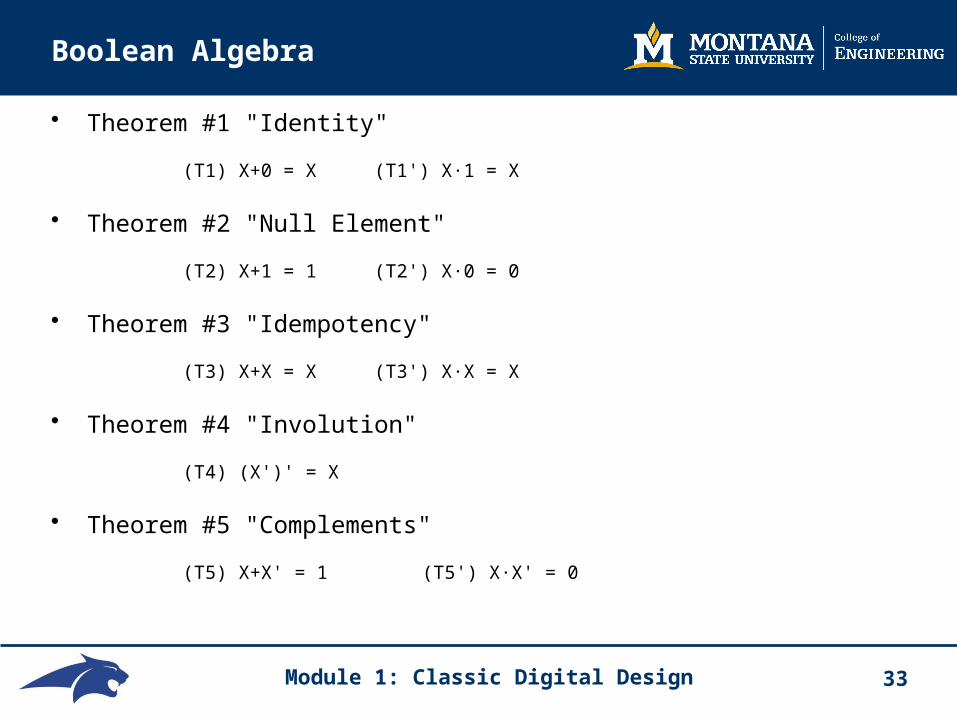
Module 1: Classic Digital Design 33
Boolean Algebra
• Theorem #1 "Identity" (T1) X+0 = X (T1') X·1 = X
• Theorem #2 "Null Element" (T2) X+1 = 1 (T2') X·0 = 0
• Theorem #3 "Idempotency" (T3) X+X = X (T3') X·X = X
• Theorem #4 "Involution" (T4) (X')' = X
• Theorem #5 "Complements" (T5) X+X' = 1 (T5') X·X' = 0
Module 1: Classic Digital Design 34
Boolean Algebra
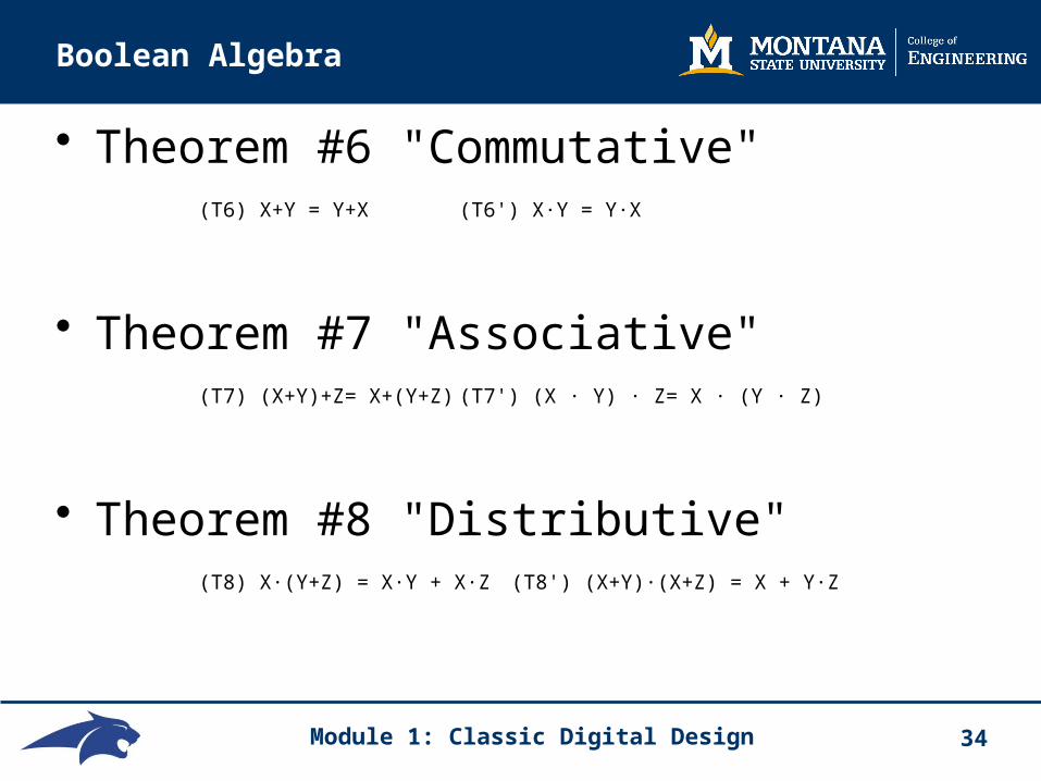
• Theorem #6 "Commutative" (T6) X+Y = Y+X (T6') X·Y = Y·X
• Theorem #7 "Associative" (T7) (X+Y)+Z= X+(Y+Z) (T7') (X · Y) · Z= X · (Y · Z)
• Theorem #8 "Distributive" (T8) X·(Y+Z) = X·Y + X·Z (T8') (X+Y)·(X+Z) = X + Y·Z
Module 1: Classic Digital Design 35
Boolean Algebra
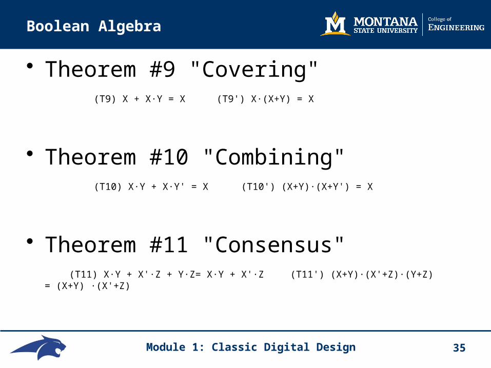
• Theorem #9 "Covering" (T9) X + X·Y = X (T9') X·(X+Y) = X
• Theorem #10 "Combining" (T10) X·Y + X·Y' = X (T10') (X+Y)·(X+Y') = X
• Theorem #11 "Consensus"
(T11) X·Y + X'·Z + Y·Z= X·Y + X'·Z (T11') (X+Y)·(X'+Z)·(Y+Z) = (X+Y) ·(X'+Z)
Module 1: Classic Digital Design 36
Boolean Algebra
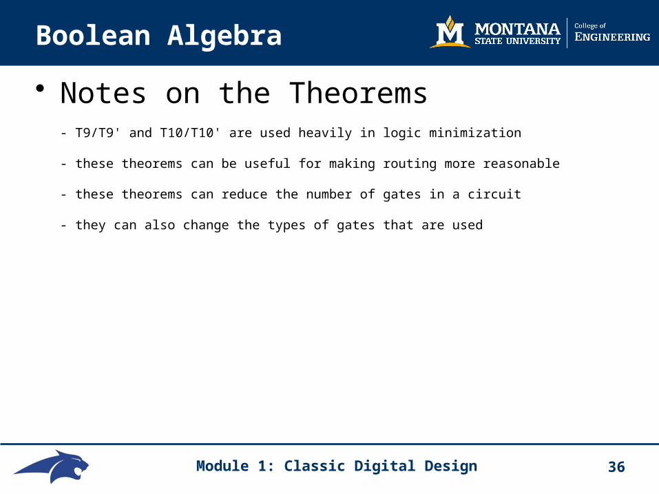
• Notes on the Theorems- T9/T9' and T10/T10' are used heavily in logic minimization
- these theorems can be useful for making routing more reasonable
- these theorems can reduce the number of gates in a circuit
- they can also change the types of gates that are used

Module 1: Classic Digital Design 37
Boolean Algebra
• More Theorem's - there are more generalized theorems available for large number of variables
T13, T14, T15
- one of the most useful is called "DeMorgan's Theorem"
• DeMorgan's Theorem - this theorem states a method to convert between AND and OR gates using inversions on the input / output
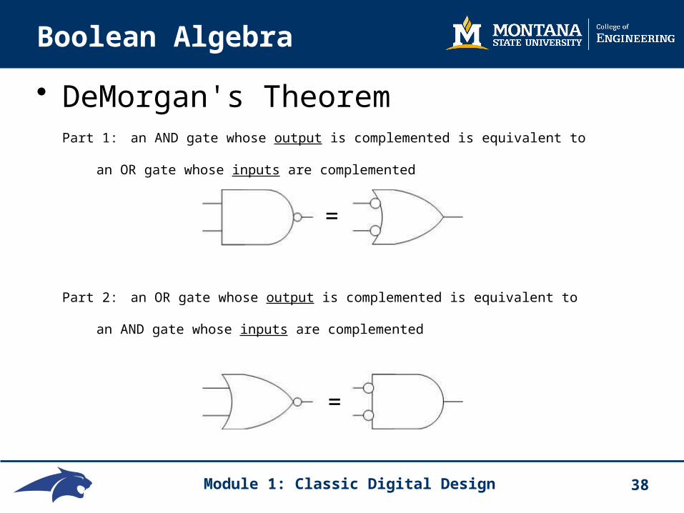
Module 1: Classic Digital Design 38
Boolean Algebra
• DeMorgan's TheoremPart 1: an AND gate whose output is complemented is equivalent to
an OR gate whose inputs are complemented
Part 2: an OR gate whose output is complemented is equivalent to
an AND gate whose inputs are complemented
=
=

Module 1: Classic Digital Design 39
Boolean Algebra
• Complement- complementing a logic function will give outputs that are inverted versions of the original function
ex) A B F F'
0 0 0 1 0 1 0 1 1 0 0 1 1 1 1 0
- DeMorgan's Theorem also gives us a generic formula to complement any expression:
- for a Logic function F, we can get F' by :
1) Swapping all + and ·
2) Complementing all Variables
- KEEP THE PARENTHESIS ORDER OF THE ORGINAL FUNCTION !!!

Module 1: Classic Digital Design 40
Boolean Algebra
• Complement- Example: Complement the Function F
ex) A B F F'
0 0 0 1 0 1 0 1 1 0 0 1 1 1 1 0
We know:
F = A · B
We swap + and · first, then we complement all variables
F' = A' + B'
- This is the same as putting an inversion bubble on the output of the logic diagram
→
Module 1: Classic Digital Design 41
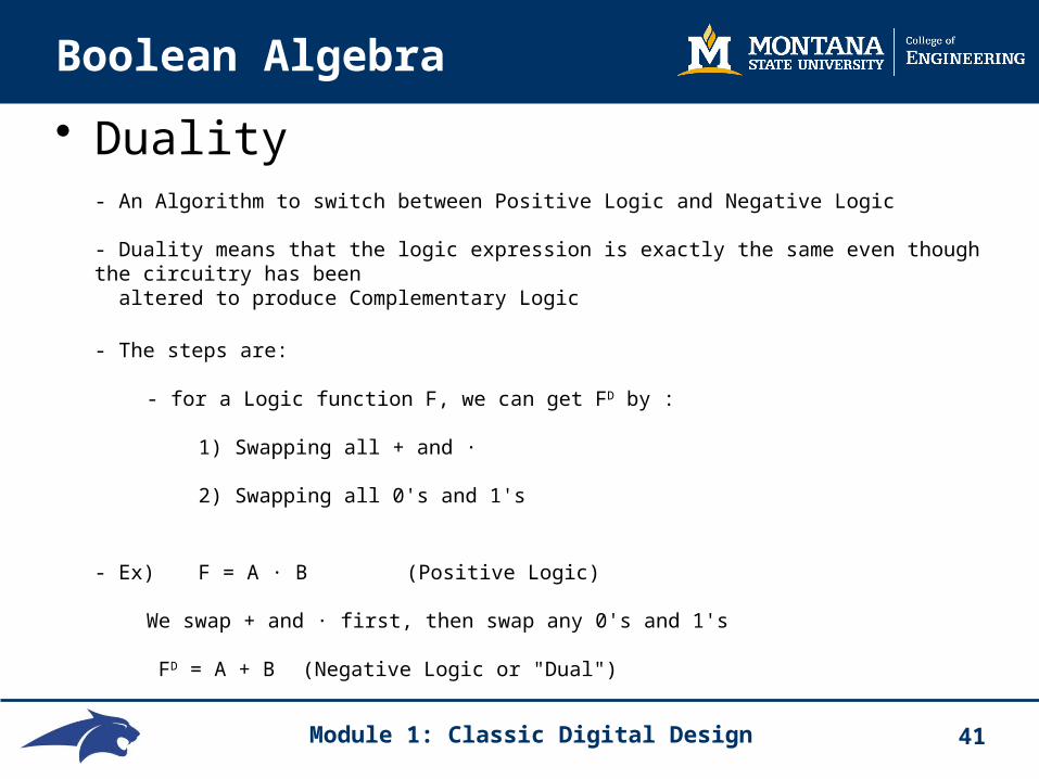
Boolean Algebra
• Duality- An Algorithm to switch between Positive Logic and Negative Logic
- Duality means that the logic expression is exactly the same even though the circuitry has been altered to produce Complementary Logic
- The steps are:
- for a Logic function F, we can get FD by :
1) Swapping all + and ·
2) Swapping all 0's and 1's
- Ex) F = A · B (Positive Logic)
We swap + and · first, then swap any 0's and 1's
FD = A + B (Negative Logic or "Dual")

Module 1: Classic Digital Design 42
Boolean Algebra
• Complement vs. Duality, What is the difference?

Module 1: Classic Digital Design 43
Minterms
• Truth Tables
Row A B C F 0 0 0 0 1 Row We assign a "Row Number" for each entry starting at 0 1 0 0 1 0 2 0 1 0 0 Variables We enter all input combinations in ascending order. 3 0 1 1 1 We use straight binary with the MSB on the left
4 1 0 0 1
5 1 0 1 0 Function We say the output is a function of the input variables
6 1 1 0 1 F(A,B,C)
7 1 1 1 1
n = the number of input variables
2n = the number of input combinations

Module 1: Classic Digital Design 44
Minterms
• Let's also define the following termsLiteral = a variable or the complement of a variable ex) A, B, C, A', B', C'
Product Term = a single literal or Logical Product of two or more literals ex) A A·B B'·C
Sum or Products = (SOP), the Logical Sum of Product Terms ex) A + B A·B + B'·C

Module 1: Classic Digital Design 45
Minterms
• Minterm
- a normal product term w/ n-literals
- a Minterm is written for each ROW in the truth table
- there are 2n Minterms for a given truth table
- we write the literals as follows:
- if the input variable is a 0 in the ROW, we complement the Minterm literal
- if the input variable is a 1 in the ROW, we do not complement the Minterm literal
- for each ROW, we use a Logical Product on all of the literals to create the Minterm

Module 1: Classic Digital Design 46
Minterms
• Minterm Row A B C Minterm F
0 0 0 0 A'·B'·C' F(0,0,0) 1 0 0 1 A'·B'·C F(0,0,1) 2 0 1 0 A'·B·C' F(0,1,0) 3 0 1 1 A'·B·C F(0,1,1) 4 1 0 0 A·B'·C' F(1,0,0) 5 1 0 1 A·B'·C F(1,0,1) 6 1 1 0 A·B·C' F(1,1,0) 7 1 1 1 A·B·C F(1,1,1)
• Canonical Sum- we Logically Sum all Minterms that correspond to a Logic 1 on the output
- the Canonical Sum represents the entire Logic Expression when the Output is TRUE
- this is called the "Sum of Products" or SOP
Module 1: Classic Digital Design 47
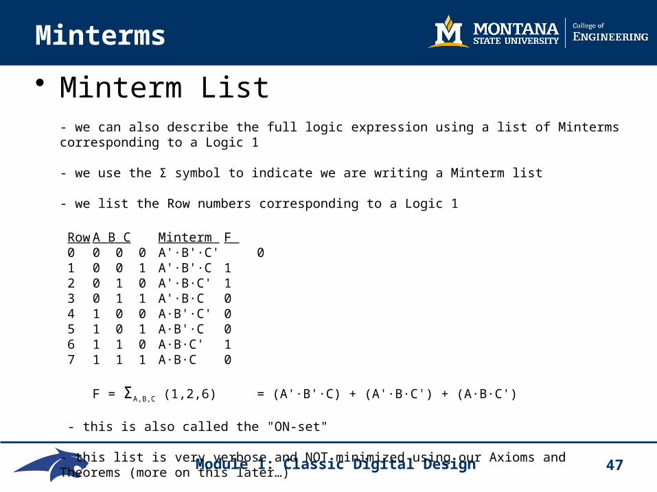
Minterms
• Minterm List- we can also describe the full logic expression using a list of Minterms corresponding to a Logic 1
- we use the Σ symbol to indicate we are writing a Minterm list
- we list the Row numbers corresponding to a Logic 1
Row A B C Minterm F 0 0 0 0 A'·B'·C' 0 1 0 0 1 A'·B'·C 1 2 0 1 0 A'·B·C' 1 3 0 1 1 A'·B·C 0 4 1 0 0 A·B'·C' 0 5 1 0 1 A·B'·C 0 6 1 1 0 A·B·C' 1 7 1 1 1 A·B·C 0
F = ΣA,B,C (1,2,6) = (A'·B'·C) + (A'·B·C') + (A·B·C')
- this is also called the "ON-set"
- this list is very verbose and NOT minimized using our Axioms and Theorems (more on this later…)

Module 1: Classic Digital Design 48
Maxterms
• Let's define the following termsSum Term = a single literal or a Logical Sum of two or more literals
ex) A A + B'
Product of Sums = (POS), the Logical Product of Sum Terms
ex) (A+B)·(B'+C)
Normal Term = a term in which no variable appears more than once
ex) "Normal
A·BA + B'
ex) "Non-Normal"
A·B·B'A + A'

Module 1: Classic Digital Design 49
Maxterms
• Maxterm - a Normal Sum Term w/ n-literals
- a Maxterm is written for each ROW in the truth table
- there are 2n Maxterms for a given truth table
- we write the literals as follows:
- if the input variable is a 0 in the ROW, we do not complement the Maxterm literal
- if the input variable is a 1 in the ROW, we complement the Maxterm literal
- for each ROW, we use a Logical Sum on all of the literals to create the Maxterm

Module 1: Classic Digital Design 50
Maxterms
• Maxterm Row A B C Minterm Maxterm F
0 0 0 0 A'·B'·C' A+B+C F(0,0,0) 1 0 0 1 A'·B'·C A+B+C' F(0,0,1) 2 0 1 0 A'·B·C' A+B'+C F(0,1,0) 3 0 1 1 A'·B·C A+B'+C' F(0,1,1) 4 1 0 0 A·B'·C' A'+B+C F(1,0,0) 5 1 0 1 A·B'·C A'+B+C' F(1,0,1) 6 1 1 0 A·B·C' A'+B'+C F(1,1,0) 7 1 1 1 A·B·C A'+B'+C' F(1,1,1)
• Canonical Product- we Logically Multiply all Maxterms that correspond to a Logic 0 on the output
- the Canonical Product represents the entire Logic Expression when the Output is TRUE
- this is called the "Product of Sums" or POS
Module 1: Classic Digital Design 51
Maxterms
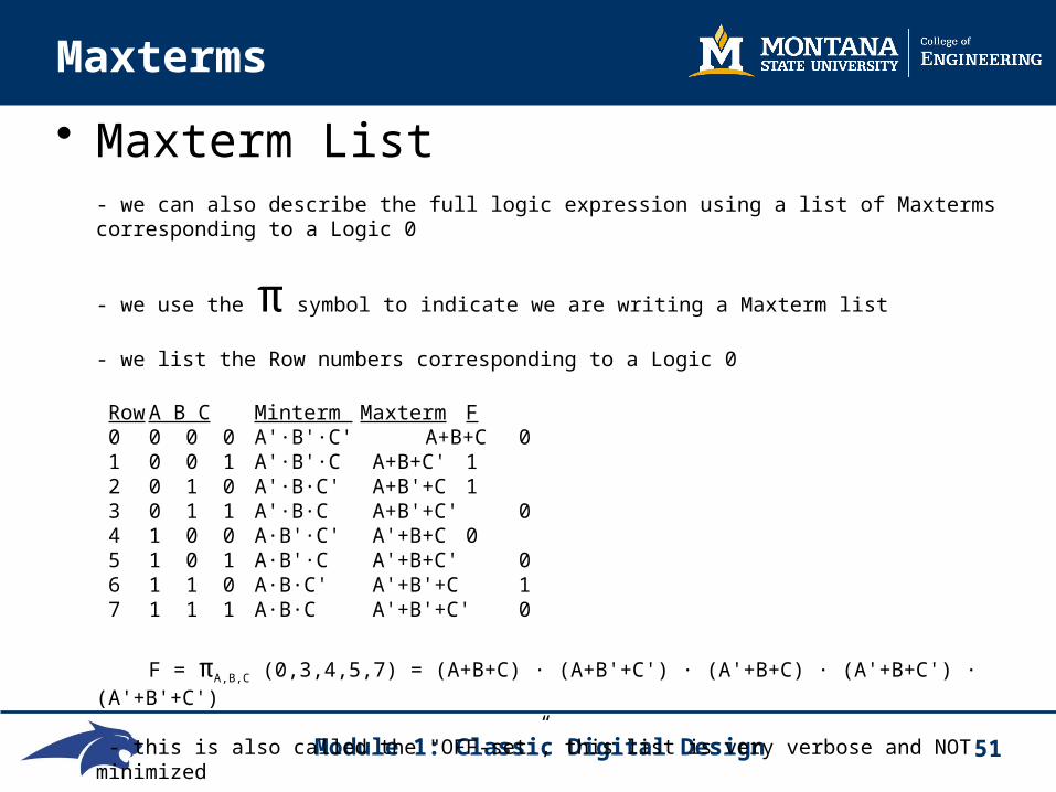
• Maxterm List- we can also describe the full logic expression using a list of Maxterms corresponding to a Logic 0
- we use the π symbol to indicate we are writing a Maxterm list
- we list the Row numbers corresponding to a Logic 0
Row A B C Minterm Maxterm F 0 0 0 0 A'·B'·C' A+B+C 0 1 0 0 1 A'·B'·C A+B+C' 1 2 0 1 0 A'·B·C' A+B'+C 1 3 0 1 1 A'·B·C A+B'+C' 0 4 1 0 0 A·B'·C' A'+B+C 0 5 1 0 1 A·B'·C A'+B+C' 0 6 1 1 0 A·B·C' A'+B'+C 1 7 1 1 1 A·B·C A'+B'+C' 0
F = πA,B,C (0,3,4,5,7) = (A+B+C) · (A+B'+C') · (A'+B+C) · (A'+B+C') · (A'+B'+C')
- this is also called the "OFF-set”, this list is very verbose and NOT minimized
Module 1: Classic Digital Design 52
Maxterms
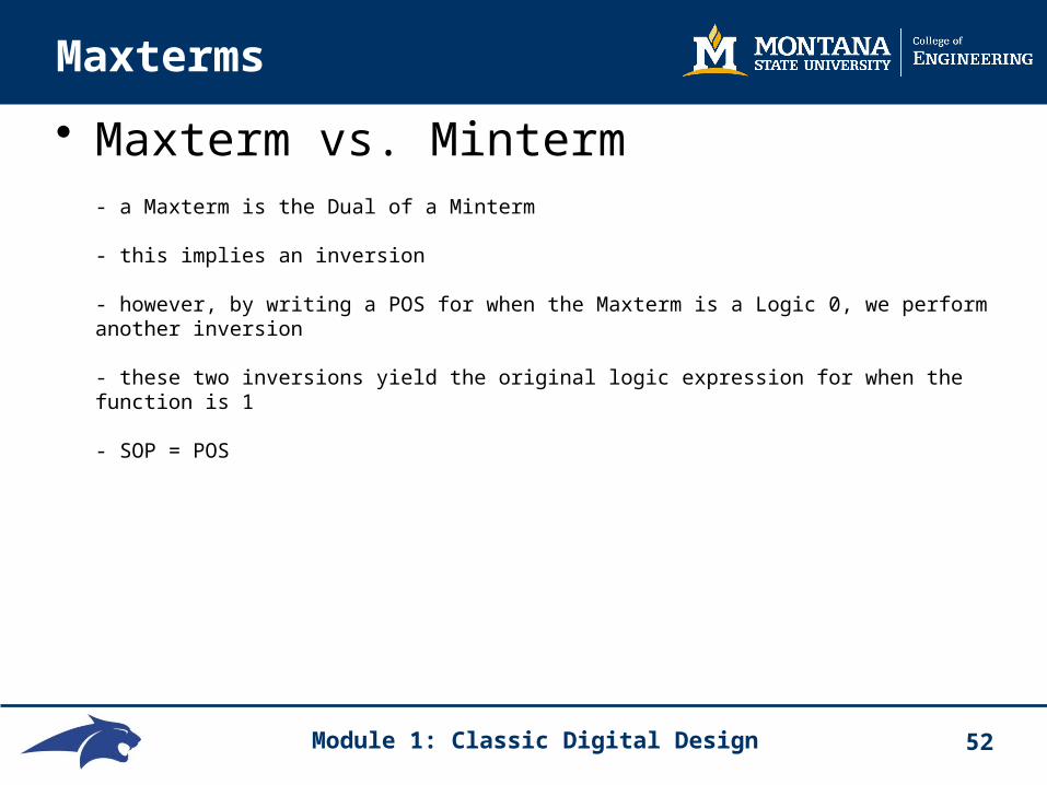
• Maxterm vs. Minterm- a Maxterm is the Dual of a Minterm
- this implies an inversion
- however, by writing a POS for when the Maxterm is a Logic 0, we perform another inversion
- these two inversions yield the original logic expression for when the function is 1
- SOP = POS

Module 1: Classic Digital Design 53
Maxterms
• Minterms & Maxterm- we now have 5 ways to describe a Logic Expression
1) Truth Table 2) Minterm List 3) Canonical Sum 4) Maxterm List 5) Canonical Product
- these all give the same information
• Converting Between Minterms and Maxterms- Minterms and Maxterms are Duals
- this means we can convert between then easily using DeMorgan's duality theorem
- converting a SOP to its dual gives Negative Logic
- converting a POS to its dual gives Negative Logic

Module 1: Classic Digital Design 54
Circuit Synthesis
• Circuit Synthesis - there are 5 ways to describe a Logic Expression
1) Truth Table 2) Minterm List 3) Canonical Sum 4) Maxterm List 5) Canonical Product
- we can directly synthesis circuits from SOP and POS expressions
SOP = AND-OR structure POS = OR-AND structure
Module 1: Classic Digital Design 55
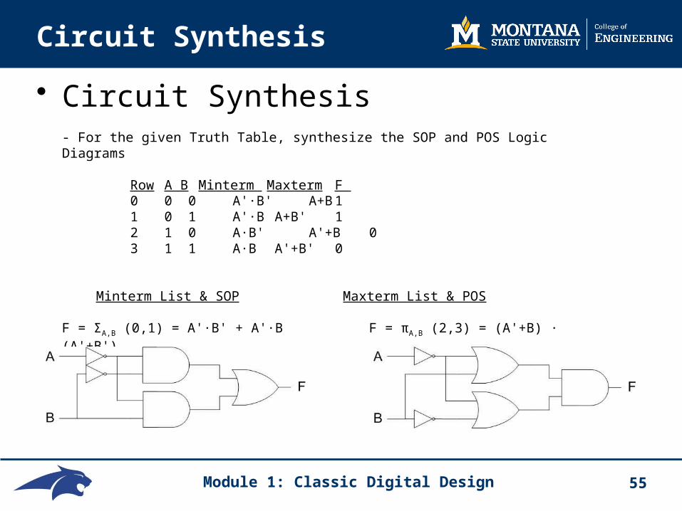
Circuit Synthesis
• Circuit Synthesis - For the given Truth Table, synthesize the SOP and POS Logic Diagrams
Row A B Minterm Maxterm F 0 0 0 A'·B' A+B 1 1 0 1 A'·B A+B' 1 2 1 0 A·B' A'+B 0 3 1 1 A·B A'+B' 0
Minterm List & SOP Maxterm List & POS
F = ΣA,B (0,1) = A'·B' + A'·B F = πA,B (2,3) = (A'+B) · (A'+B')
Module 1: Classic Digital Design 56
Circuit Synthesis
• Circuit Manipulation - we can manipulate our Logic Diagrams to give the same logic expression but use different logic gates
- this can be important when using technologies that:
- only have certain gates (i.e., INV, NAND, NOR) - have certain gates that are faster than others (i.e., NAND-NAND, NOR-NOR)
- we can convert a SOP/POS logic diagram into a NAND-NAND or NOR-NOR structure

Module 1: Classic Digital Design 57
Circuit Synthesis
• Common Circuit Manipulation "DeMorgan's"
=
=
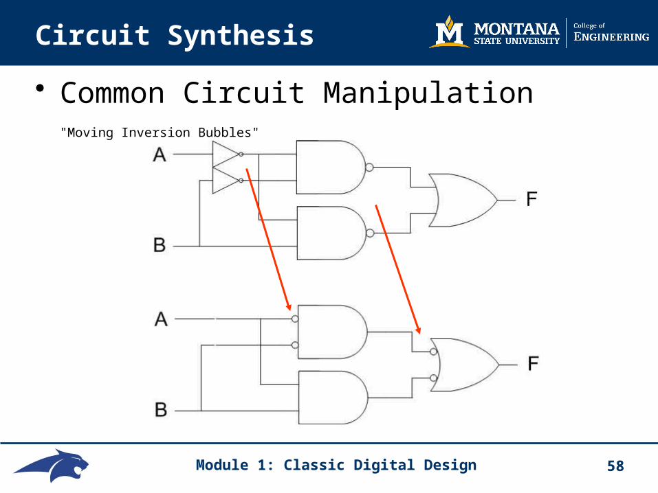
Module 1: Classic Digital Design 58
Circuit Synthesis
• Common Circuit Manipulation "Moving Inversion Bubbles"

Module 1: Classic Digital Design 59
Circuit Synthesis
• Common Circuit Manipulation "Inserting Double Inversion Bubbles"

Module 1: Classic Digital Design 60
Circuit Synthesis
• Common Circuit Manipulation "Bubbles can be moved to either side of an Inverter"

Module 1: Classic Digital Design 61
Logic Minimization
• Logic Minimization- We've seen that we can directly translate a Truth Table into a SOP/POS and in turn a Logic Diagram
- However, this type of expression is NOT minimized
ex) Row A B Minterm Maxterm F 0 0 0 A'·B' A+B 1 1 0 1 A'·B A+B' 1 2 1 0 A·B' A'+B 0 3 1 1 A·B A'+B' 0
Minterm List & SOP Maxterm List & POS
F = ΣA,B (0,1) = A'·B' + A'·B F = πA,B (2,3) = (A'+B) · (A'+B')

Module 1: Classic Digital Design 62
Logic Minimization
• Logic Minimization- using our Axioms and Theorems, we can manually minimize the expressions…
Minterm List & SOP Maxterm List & POS
F = A'·B' + A'·B F = (A'+B) · (A'+B')
F = A'·(B'+B) = A' F = A' + (B'·B) = A'
- doing this by hand can be difficult and requires that we recognize patterns associated with our 5 Axioms and our 15+ Theorems
• Karnaugh Maps- a graphical technique to minimize a logic expression
Module 1: Classic Digital Design 63
Logic Minimization
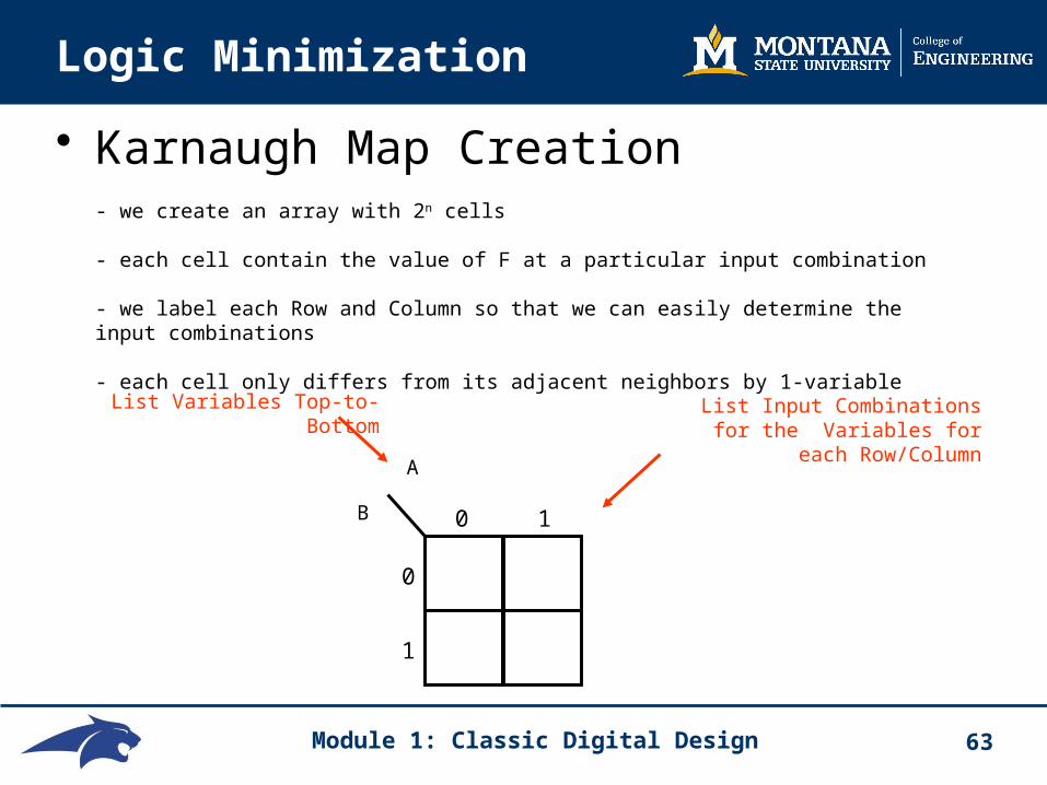
• Karnaugh Map Creation- we create an array with 2n cells
- each cell contain the value of F at a particular input combination
- we label each Row and Column so that we can easily determine the input combinations
- each cell only differs from its adjacent neighbors by 1-variable
A
B 0 1
0
1
List Variables Top-to-Bottom List Input Combinations for the Variables for each Row/Column

Module 1: Classic Digital Design 64
Logic Minimization
• Karnaugh Map CreationA
B 0 1
0
1
We can put redundant labeling for when a variable is TRUE. This helps when creating
larger K-maps
We can also put the Truth Table Row number so that copying the Truth Table
values into the K-map is straight-forward
0
1
2
3
B
A

Module 1: Classic Digital Design 65
Logic Minimization
• Karnaugh Map Creation- we can now copy in the Function values
Row A B Minterm Maxterm F 0 0 0 A'·B' A+B 11 0 1 A'·B A+B' 12 1 0 A·B' A'+B 03 1 1 A·B A'+B' 0
- at this point, the K-map is simply the same information as in the Truth Table
- we could write a SOP or POS directly from the K-map if we wanted to
1 0
1 0
A
B 0 1
0
1
0
1
2
3
B
A

Module 1: Classic Digital Design 66
Logic Minimization
• Karnaugh Map Creation- we can create 3 variable K-Maps
- notice the input combination numbering in order to achieve no more than 1-variable difference between cells
AB
C 00 01
0
1
0
1
2
3
C
A
6
7
4
5
11 10
B
Module 1: Classic Digital Design 67
Logic Minimization
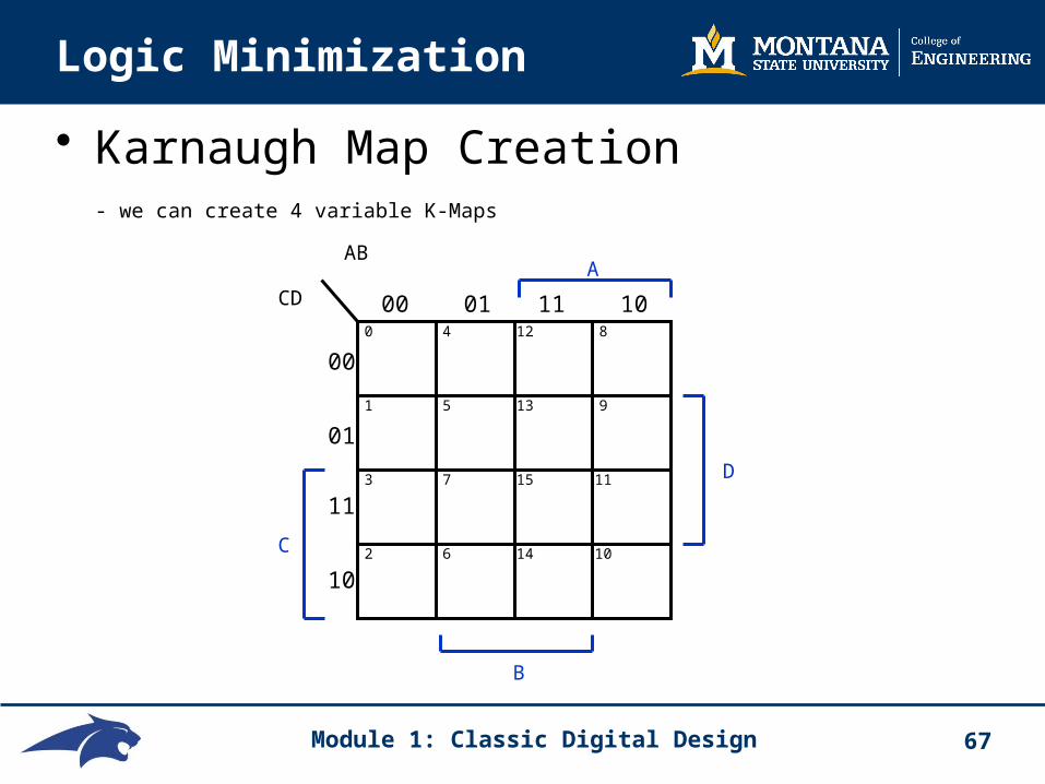
• Karnaugh Map Creation- we can create 4 variable K-Maps
AB
CD 00 01
00
01
0
1
4
5
C
A
12
13
8
9
11 10
B
3
2
7
6
15
14
11
10
11
10
D
Module 1: Classic Digital Design 68
Logic Minimization
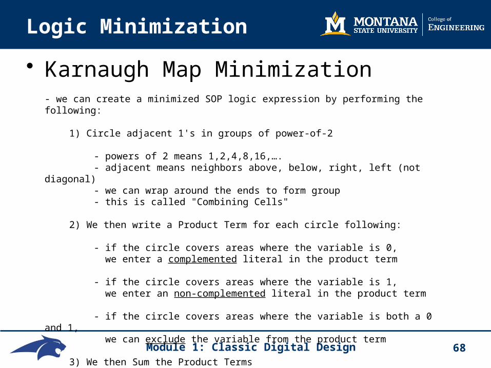
• Karnaugh Map Minimization- we can create a minimized SOP logic expression by performing the following:
1) Circle adjacent 1's in groups of power-of-2
- powers of 2 means 1,2,4,8,16,…. - adjacent means neighbors above, below, right, left (not diagonal) - we can wrap around the ends to form group - this is called "Combining Cells"
2) We then write a Product Term for each circle following:
- if the circle covers areas where the variable is 0, we enter a complemented literal in the product term - if the circle covers areas where the variable is 1, we enter an non-complemented literal in the product term
- if the circle covers areas where the variable is both a 0 and 1, we can exclude the variable from the product term
3) We then Sum the Product Terms

Module 1: Classic Digital Design 69
Logic Minimization
• Karnaugh Map Minimization- let's write a minimized SOP for the following K-map
1 0
1 0
A
B 0 1
0
1
0
1
2
3
B
A
- this circle covers 2 cells- the circle covers:
- where A=0, so the literal is A'- where B=0 and 1, so the literal is excluded
- our final SOP expression is
F = A'
Module 1: Classic Digital Design 70
Logic Minimization
• Karnaugh Map Minimization
0 1
1 0
AB
C 00 01
0
1
0
1
2
3
C
A
0
1
6
7
0
1
4
5
11 10
B
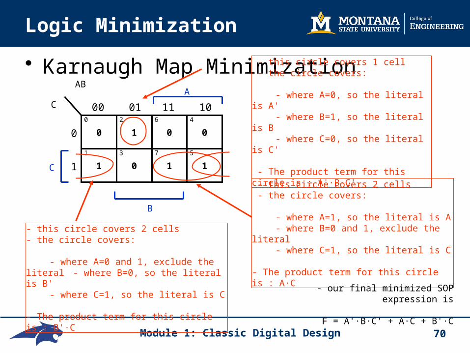
- this circle covers 1 cell - the circle covers:
- where A=0, so the literal is A'- where B=1, so the literal is B
- where C=0, so the literal is C'
- The product term for this circle is : A'·B·C'
- this circle covers 2 cells - the circle covers:
- where A=1, so the literal is A- where B=0 and 1, exclude the literal
- where C=1, so the literal is C
- The product term for this circle is : A·C
- this circle covers 2 cells- the circle covers:
- where A=0 and 1, exclude the literal - where B=0, so the literal is B'
- where C=1, so the literal is C
- The product term for this circle is : B'·C
- our final minimized SOP expression is
F = A'·B·C' + A·C + B'·C
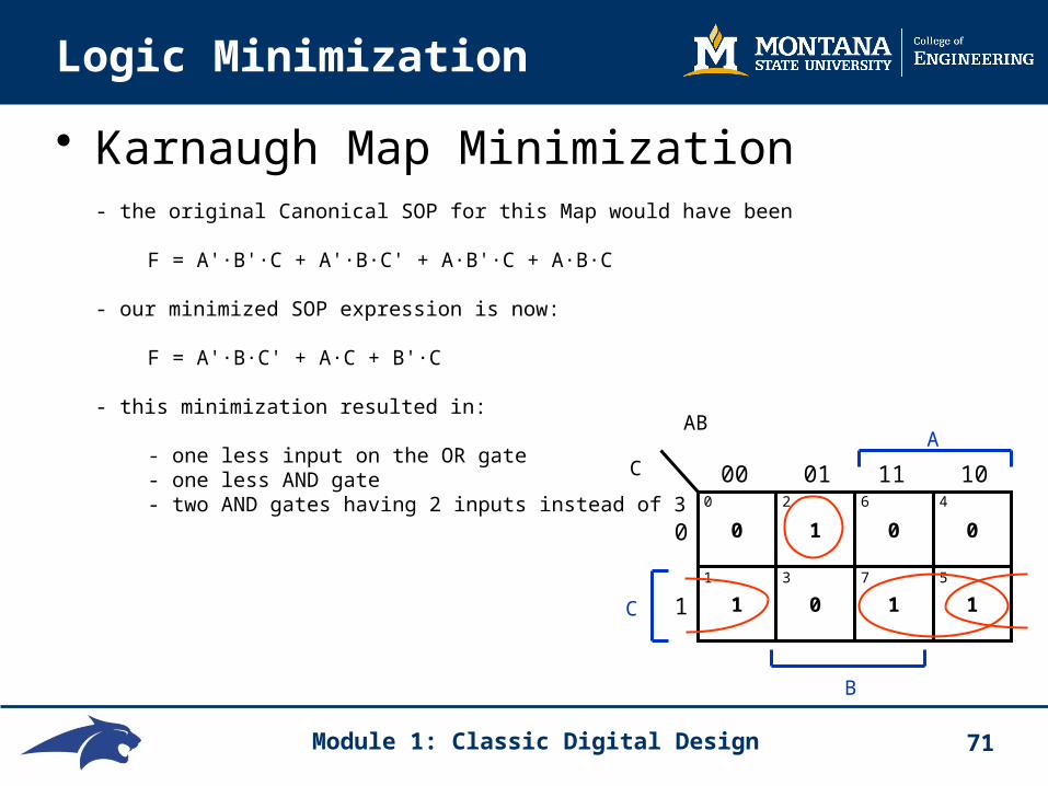
Module 1: Classic Digital Design 71
Logic Minimization
• Karnaugh Map Minimization- the original Canonical SOP for this Map would have been
F = A'·B'·C + A'·B·C' + A·B'·C + A·B·C
- our minimized SOP expression is now:
F = A'·B·C' + A·C + B'·C
- this minimization resulted in:
- one less input on the OR gate - one less AND gate - two AND gates having 2 inputs instead of 3
0 1
1 0
AB
C 00 01
0
1
0
1
2
3
C
A
0
1
6
7
0
1
4
5
11 10
B

Module 1: Classic Digital Design 72
Logic Minimization
• 2-Variable K-Map Example- write a minimal SOP for the following truth table
Row A B Minterm Maxterm F 0 0 0 A'·B' A+B 01 0 1 A'·B A+B' 12 1 0 A·B' A'+B 13 1 1 A·B A'+B' 1
- we first copy in the output values into the K-map
0 1
1 1
A
B 0 1
0
1
0
1
2
3
B
A

Module 1: Classic Digital Design 73
Logic Minimization
• 2-Variable K-Map Example - we then circle groups of 1's in order to find the Product Term for each circle
0 1
1 1
A
B 0 1
0
1
0
1
2
3
B
A - this circle covers 2 cells - the circle covers:
- where A=1, so the literal is A- where B=0 and 1, exclude the literal
- The product term for this circle is : A
- this circle covers 2 cells - the circle covers:
- where A=0 and 1, exclude the literal - where B=1, so the literal is B
- The product term for this circle is : B
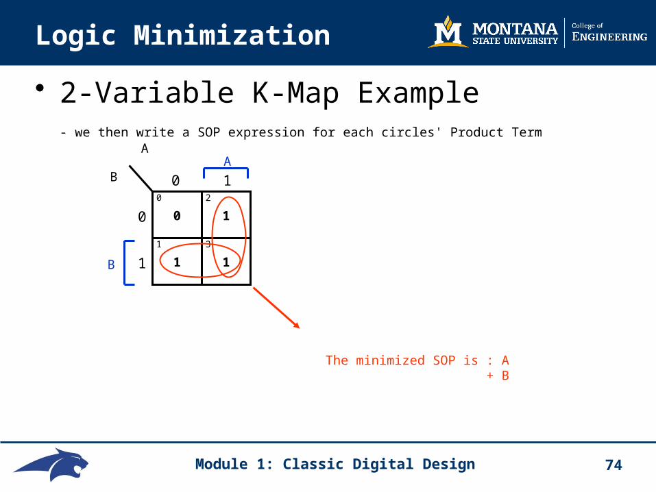
Module 1: Classic Digital Design 74
Logic Minimization
• 2-Variable K-Map Example - we then write a SOP expression for each circles' Product Term
0 1
1 1
A
B 0 1
0
1
0
1
2
3
B
A
The minimized SOP is : A + B

Module 1: Classic Digital Design 75
Logic Minimization
• 3-Variable K-Map Example - write a minimal SOP expression for the following truth table
Row A B C Minterm Maxterm F 0 0 0 0 A'·B'·C' A+B+C 0 1 0 0 1 A'·B'·C A+B+C' 1 2 0 1 0 A'·B·C' A+B'+C 1 3 0 1 1 A'·B·C A+B'+C' 0 4 1 0 0 A·B'·C' A'+B+C 1 5 1 0 1 A·B'·C A'+B+C' 1 6 1 1 0 A·B·C' A'+B'+C 1 7 1 1 1 A·B·C A'+B'+C' 1
0 1
1 0
AB
C 00 01
0
1
0
1
2
3
C
A
1
1
6
7
1
1
4
5
11 10
B
Module 1: Classic Digital Design 76
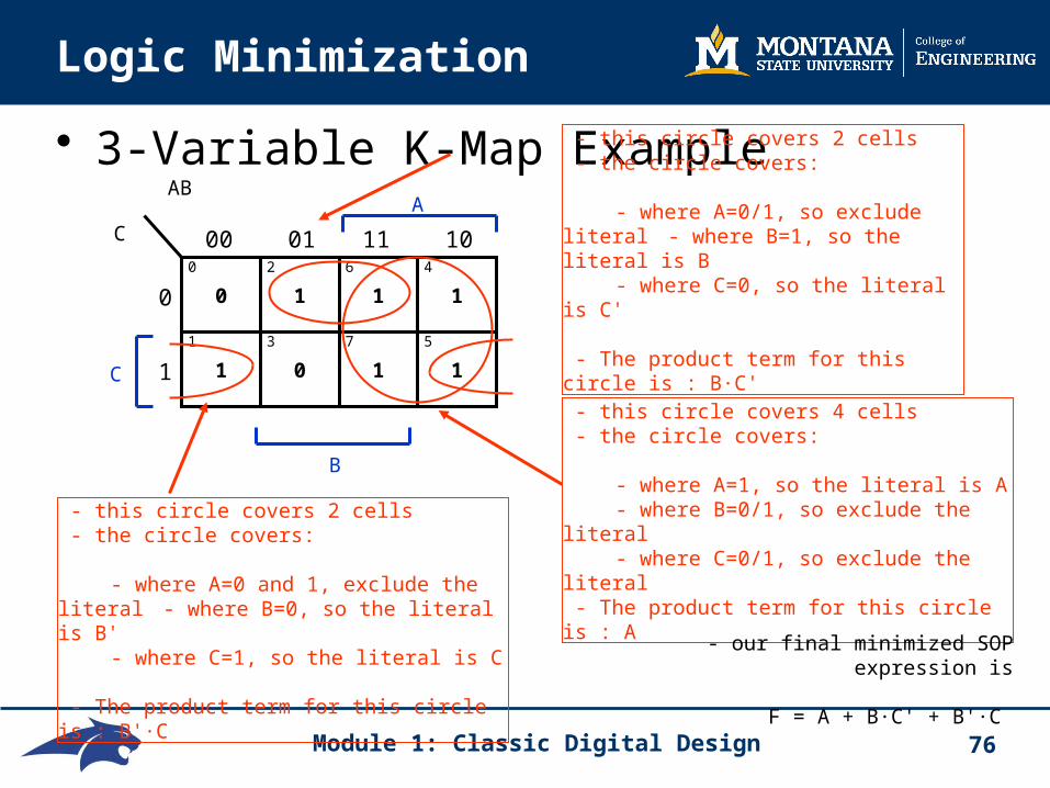
Logic Minimization
• 3-Variable K-Map Example
0 1
1 0
AB
C 00 01
0
1
0
1
2
3
C
A
1
1
6
7
1
1
4
5
11 10
B
- this circle covers 2 cells - the circle covers:
- where A=0/1, so exclude literal- where B=1, so the literal is B
- where C=0, so the literal is C'
- The product term for this circle is : B·C'
- this circle covers 4 cells - the circle covers:
- where A=1, so the literal is A- where B=0/1, so exclude the literal
- where C=0/1, so exclude the literal - The product term for this circle is : A
- this circle covers 2 cells - the circle covers:
- where A=0 and 1, exclude the literal - where B=0, so the literal is B'
- where C=1, so the literal is C
- The product term for this circle is : B'·C
- our final minimized SOP expression is
F = A + B·C' + B'·C

Module 1: Classic Digital Design 77
Logic Minimization
• 4-Variable K-Map Example
- write a minimal SOP expression for the following truth table Row A B C D F 0 0 0 0 0 0 1 0 0 0 1 1 2 0 0 1 0 0 3 0 0 1 1 1 4 0 1 0 0 0 5 0 1 0 1 0 6 0 1 1 0 0 7 0 1 1 1 0 8 1 0 0 0 1 9 1 0 0 1 1 10 1 0 1 0 1 11 1 0 1 1 1 12 1 1 0 0 0 13 1 1 0 1 0 14 1 1 1 0 0 15 1 1 1 1 0
0 0
1 0
AB
CD 00 01
00
01
0
1
4
5
C
A
0
0
12
13
1
1
8
9
11 10
B
1 0
0 0
3
2
7
6
0
0
15
14
1
1
11
10
11
10
D
Module 1: Classic Digital Design 78
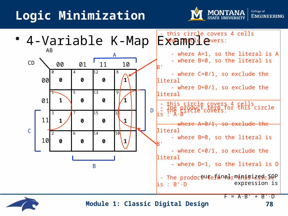
Logic Minimization
• 4-Variable K-Map Example
0 0
1 0
AB
CD 00 01
00
01
0
1
4
5
C
A
0
0
12
13
1
1
8
9
11 10
B
1 0
0 0
3
2
7
6
0
0
15
14
1
1
11
10
11
10
D
- this circle covers 4 cells - the circle covers:
- where A=1, so the literal is A- where B=0, so the literal is B'
- where C=0/1, so exclude the literal - where D=0/1, so exclude the literal
- The product term for this circle is : A·B'
- this circle covers 4 cells - the circle covers:
- where A=0/1, so exclude the literal - where B=0, so the literal is B'
- where C=0/1, so exclude the literal - where D=1, so the literal is D
- The product term for this circle is : B'·D
- our final minimized SOP expression is
F = A·B' + B'·D

Module 1: Classic Digital Design 79
Logic Minimization
• K-Map Logic Minimization- we can use K-maps to write a minimal SOP (and POS)
- however, we've seen that there is a potential for redundant Product Terms
- we need to define what it is to be "Minimized"
0 0
0 1
AB
C 00 01
0
1
0
1
2
3
C
A
1
1
6
7
1
0
4
5
11 10
Is this circle necessary?
Module 1: Classic Digital Design 80
Logic Minimization
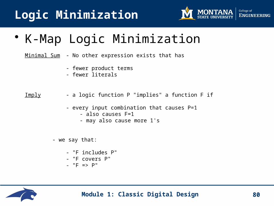
• K-Map Logic MinimizationMinimal Sum - No other expression exists that has
- fewer product terms - fewer literals
Imply - a logic function P "implies" a function F if
- every input combination that causes P=1 - also causes F=1 - may also cause more 1's
- we say that:
- "F includes P" - "F covers P" - "F => P"
Module 1: Classic Digital Design 81
Logic Minimization
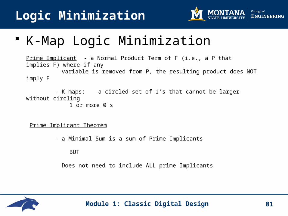
• K-Map Logic MinimizationPrime Implicant - a Normal Product Term of F (i.e., a P that implies F) where if any variable is removed from P, the resulting product does NOT imply F
- K-maps: a circled set of 1's that cannot be larger without circling 1 or more 0's
Prime Implicant Theorem
- a Minimal Sum is a sum of Prime Implicants
BUT Does not need to include ALL prime Implicants

Module 1: Classic Digital Design 82
Logic Minimization
• K-Map Logic MinimizationComplete Sum - the product of all Prime Implicants (not minimized)
Distinguished 1-Cell
- an "input combination" that is covered by only ONE Prime Implicant
Essential Prime Implicant
- a Prime Implicant that covers one or more "Distinguished 1-Cells"
NOTE: - the sum of Essential Prime Implicants is the Minimal Sum
- this means we're done minimizing

Module 1: Classic Digital Design 83
Logic Minimization
• K-Map Logic MinimizationSteps for Minimization
1) Identify All Prime Implicants
2) Identify the Distinguished 1-Cells
3) Identify the Essential Prime Implicants
4) Create the SOP using Essential Prime Implicants
Module 1: Classic Digital Design 84
Logic Minimization
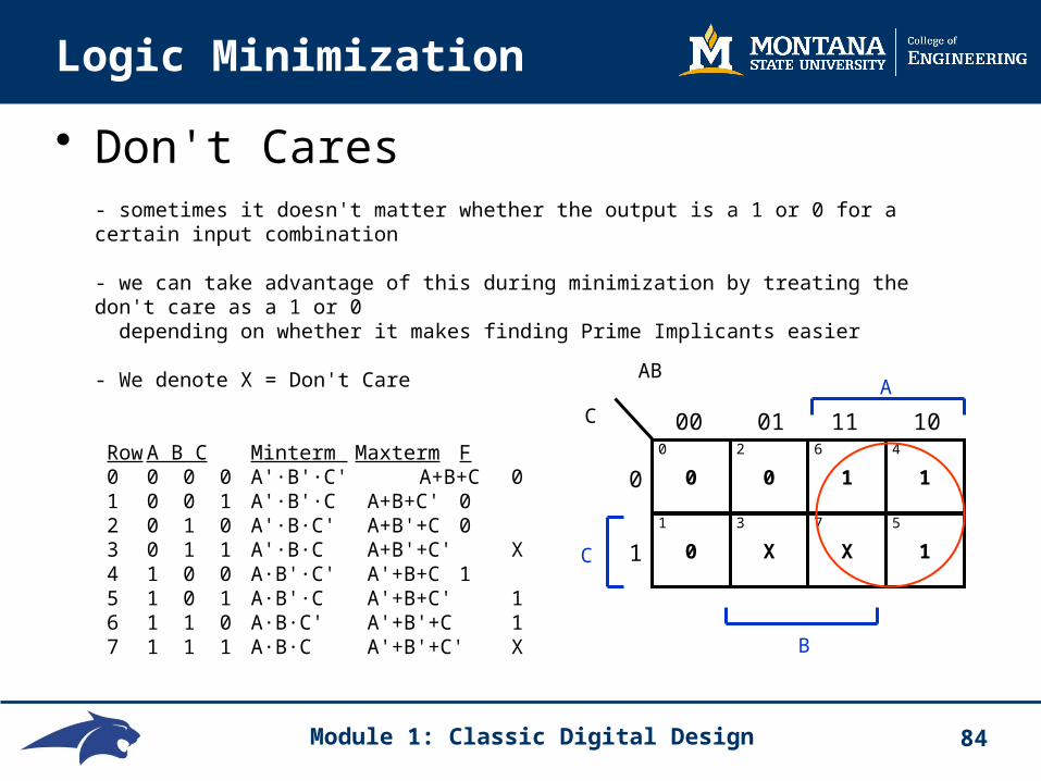
• Don't Cares- sometimes it doesn't matter whether the output is a 1 or 0 for a certain input combination
- we can take advantage of this during minimization by treating the don't care as a 1 or 0 depending on whether it makes finding Prime Implicants easier
- We denote X = Don't Care
Row A B C Minterm Maxterm F 0 0 0 0 A'·B'·C' A+B+C 0 1 0 0 1 A'·B'·C A+B+C' 0 2 0 1 0 A'·B·C' A+B'+C 0 3 0 1 1 A'·B·C A+B'+C' X 4 1 0 0 A·B'·C' A'+B+C 1 5 1 0 1 A·B'·C A'+B+C' 1 6 1 1 0 A·B·C' A'+B'+C 1 7 1 1 1 A·B·C A'+B'+C' X
0 0
0 X
AB
C 00 01
0
1
0
1
2
3
C
A
1
X
6
7
1
1
4
5
11 10
B

Module 1: Classic Digital Design 85
Timing Hazards
• Hazards- we've only considered the Static (or steady state) values of combination logic
- in reality, there is delay present in the gates
- this can cause different paths through the circuit which arrive at different times at the input to a gate
- this delay can cause an unwanted transition or "glitch" on the output of the circuit
- this behavior is known as a "Timing Hazard"
- a Hazard is the possibility of an input combination causing a glitch
Module 1: Classic Digital Design 86
Timing Hazards
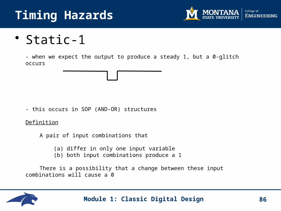
• Static-1- when we expect the output to produce a steady 1, but a 0-glitch occurs
- this occurs in SOP (AND-OR) structures
Definition
A pair of input combinations that
(a) differ in only one input variable (b) both input combinations produce a 1
There is a possibility that a change between these input combinations will cause a 0

Module 1: Classic Digital Design 87
Timing Hazards
• Static-0- when we expect the output to produce a steady 0, but a 1-glitch occurs
- this occurs in POS (OR-AND) structures
Definition
A pair of input combinations that
(a) differ in only one input variable (b) both input combinations produce a 0
There is a possibility that a change between these input combinations will cause a 1

Module 1: Classic Digital Design 88
Timing Hazards
• Hazards and K-maps- K-maps graphically show input combinations that vary by only one variable
- it is easy to see when adjacent cells have 1's and have a potential Timing Hazard
- this is a Minimal Sum, BUT, what about the transition from A·B·C to A·B·C'?
- there is a Timing Hazard present!!!
0 0
0 1
AB
C 00 01
0
1
0
1
2
3
C
A
1
1
6
7
1
0
4
5
11 10
B

Module 1: Classic Digital Design 89
Timing Hazards
• Hazards and K-maps- the solution is to add an additional product term (Prime Implicant) to cover the transition
- this ensures that the output is valid while transitioning between any input combination
- this is NOT a Minimal Sum, but it is Hazard Free
0 0
0 1
AB
C 00 01
0
1
0
1
2
3
C
A
1
1
6
7
1
0
4
5
11 10
B

Module 1: Classic Digital Design 90
Timing Hazards
• Dynamic Hazards- when we undergo a transition on the output but multiple transitions occur
- this is again due to multiple paths w/ different delays from input to output
- typically is larger leveled logic
- Solution: If the circuit is Static Hazard Free, then it is Dynamic Hazard Free

Module 1: Classic Digital Design 91
Timing Hazards
• Hazard Prevention- adding redundant Prime Implicants will prevent Hazards but can sometime add too much logic
- we can also perform delay matching through the circuit by inserting buffers so that the delay is the same at each level of logic

Module 1: Classic Digital Design 92
Design Flow
• Combinational Logic Design Flow- We now have all the pieces for a complete design process
1) Design Specifications : description of what we want to do
2) Truth Table : listing the logical operation of the system
3) Describe using : creating the logic expression SOP/POS/Minterm/Maxterm
4) Logic Minimization : K-maps
5) Logic Manipulation : Convert to desired technology (NAND/NAND, …)
6) Hazard Prevention

Module 1: Classic Digital Design 93
Sequential Logic- Concept of “Storage Element”
- With Storage, logic functions can depend on current & past values of inputs
- Sequential State Machines can be created
D-Flip-Flop
- on timing event (i.e., edge of clock input), D input goes to Q output
Sequential Logic
D Q
Q
D
Q
Q
CLK
tc2q

Module 1: Classic Digital Design 94
Finite State Machines
• Synchronous- we now have a way to store information on an edge (i.e., a flip-flop)
- we can use these storage elements to build "Synchronous Circuitry"
- Synchronous means that events occur on the edge of a clock
• State Machine- a generic name given to sequential circuit design
- it is sequential because the outputs depend on :
1) the current inputs 2) past inputs
- state machines are the basis for all modern digital electronics

Module 1: Classic Digital Design 95
Finite State Machines
• State Memory- a set of flip-flops that store the Current State of the machine
- the Current State is due to all of the input conditions that have existed since the machine started
- if there are "n" flip-flops, there can be 2n states
- a state contains everything we need to know about all past events
- we define two unique states in a machine
1) Current State 2) Next State
• Current State - the state that the machine is currently in
- this is found on the outputs of the flip-flops (i.e., Q)
Module 1: Classic Digital Design 96
Finite State Machines
• Next State- the state that the machine "will go to" upon a clock edge
- this is found on the inputs of the flip-flops (i.e., D)
- the Next State depends on
- the Current State - any Inputs
- we call the Next State Logic "F"

Module 1: Classic Digital Design 97
Finite State Machines
• State Transition- upon a clock edge, the machine changes from the "Current State" to the "Next State"
- After the clock edge, we reassign back the names (i.e., Q=Current State, D= Next State)
• State Table- a table where we list which state the machine will transition to on a clock edge
- this table depends on the "Current State" and the "Inputs"
- we can use the following notation when describing Current and Next States
Current Next S S* Scur Snxt
SC SN
Acur Bnxt
QC QN

Module 1: Classic Digital Design 98
Finite State Machines
• State Table cont…- we typically give the states of our machine descriptive names (i.e., Reset, Start, Stop, S0)
ex) State Table for a 4-state counter, no inputs
Current State Next State
S0 S1
S1 S2
S2 S3
S3 S0

Module 1: Classic Digital Design 99
Finite State Machines
• State Table cont…- when there are inputs, we list them in the table
ex) State Table for a 4-state counter with directional input
Current State Dir Next State
S0 Up S1Down S3
S1 Up S2Down S0
S2 Up S3Down S1
S3 Up S0Down S2
- we don't need to exhaustively write all of the Current States for each Input combination (i.e., Direction) which makes the table more readable

Module 1: Classic Digital Design 100
Finite State Machines
• State Variables- remember that the State Memory is just a set of flip-flops
- also remember that the state is just the current/next binary number on the in/out of the flip-flops
- we use the term State Variable to describe the input/output for a particular flip flop
- let's call our State Variables Q1, Q0, ….
Current State Dir Next State Q1 Q0 Q1* Q0*
0 0 Up 0 1Down 1 1
0 1 Up 1 0 Down 0 0
1 0 Up 1 1 Down 0 1
1 1 Up 0 0 Down 1 0

Module 1: Classic Digital Design 101
Finite State Machines
• State Variables- we call the assignment of a State name to a binary number "State Encoding"
ex) S0 = 00 S1 = 01 S2 = 10 S3 = 11
- this is arbitrary and up to use as designers
- we can choose the encoding scheme based on our application and optimize for
1) Speed 2) Power 3) Area
Module 1: Classic Digital Design 102
Finite State Machines
• Next State Logic "F"- for each "Next State" variable, we need to create logic circuitry
- this logic circuitry is combinational and has inputs:
1) Current State 2) any Inputs
ex) Q1* = F(Current State, Inputs) = F(Q1, Q0, Dir) Q0* = F(Current State, Inputs) = F(Q1, Q0, Dir)
- the logic expression for the Next State Variable is called the "Characteristic Equation" - this is a generic term that describes the logic for all flip-flops
- when we write the logic for a specific flip-flop, we call this the "Excitation Equation"
- this is a specific term that describes logic for your flip-flop (i.e., DFF)
- there will be an Excitation Equation for each Next State Variable (i.e., each Flip-Flop)

Module 1: Classic Digital Design 103
Finite State Machines
• State Variables and Next State Logic "F"- we already know how to describe combinational logic (i.e., K-maps, SOP, SOP)
- we simply apply this to our State Table
ex) State Table for a 4-state counter, no inputs
Current State Next State Q1 Q0 Q1* Q0*
0 0 0 1
0 1 1 0
1 0 1 1
1 1 0 0
- we put these inputs and outputs in a K-map and come up with Q1* = Q1 Q0
NextState
Variable
F inputs
F outputs

Module 1: Classic Digital Design 104
Finite State Machines
• State Variables and Next State Logic "F"- we continue writing Excitation Equations for each Next State Variable in our Machine
- let's now write an Excitation Equation for Q0*
ex) State Table for a 4-state counter, no inputs
Current State Next State Q1 Q0 Q1* Q0*
0 0 0 1
0 1 1 0
1 0 1 1
1 1 0 0
- we simply put these values in a K-map and come up with Q0* = Q0'
NextState
Variable
F inputs
F outputs

Module 1: Classic Digital Design 105
Finite State Machines
• Logic Diagram- the state machine just described would be implemented like this:

Module 1: Classic Digital Design 106
Finite State Machines
• Excitation Equations- we designed this State Machine using D-Flip-Flops
- this is the most common type of flip-flop and widely used in modern digital systems
- we can also use other flip-flops
- the difference is how we turn a "Characteristic Equation" into an "Excitation Equation"
- we will look at State Memory using other types of Flip-Flops later

Module 1: Classic Digital Design 107
Finite State Machines (Mealy vs. Moore)
• Output Logic "G"- last time we learned about State Memory
- we also learned about Next State Logic "F"
- the last part of our State Machine is how we create the output circuitry
- the outputs are determined by Combinational Logic that we call "G"
- there are two basic structures of output types
1) Mealy = the outputs depend on the Current State and the Inputs 2) Moore = the outputs depend on the Current State only

Module 1: Classic Digital Design 108
Finite State Machines (Mealy vs. Moore)
• State Machines“Mealy Outputs” – outputs depend on the Current State and the Inputs
- G(Current State, Inputs)

Module 1: Classic Digital Design 109
Finite State Machines (Mealy vs. Moore)
• State Machines“Moore Outputs” – outputs depend on the Current State only
- G(Current State)
Module 1: Classic Digital Design 110
Finite State Machines (Mealy vs. Moore)
• Output Logic "G"- we can create an "Output Table" for our desired results
- most often, we include the outputs in our State Table and form a hybrid "State/Output Table"
ex)
Current State In Next State Out Q1 Q0 Q1* Q0*
0 0 0 0 0 01 0 1 0
0 1 0 1 0 01 0 0 0
1 0 0 0 0 01 1 1 0
1 1 0 0 0 01 0 0 1

Module 1: Classic Digital Design 111
Finite State Machines (Mealy vs. Moore)
• State Machine Tables- officially, we use the following terms:
State Table - list of the descriptive state names and how they transition
Transition Table - using the explicitly state encoded variables and how they transition
Output Table - listing of the outputs for all possible combinations of Current States and Inputs
State/Output Table - combined table listing Current/Next states and corresponding outputs

Module 1: Classic Digital Design 112
Finite State Machines (Mealy vs. Moore)
• Output Logic "G"- we simply use the Current State and Inputs (if desired) as the inputs to G and form the logic expression (K-maps, SOP, POS) reflecting the output variable
- this is the same process as creating the Excitation Equations for the Next State Variables
ex) Current State In Next State Out Q1 Q0 Q1* Q0*
0 0 0 0 0 01 0 1 0
0 1 0 1 0 01 0 0 0
1 0 0 0 0 01 1 1 0
1 1 0 0 0 01 0 0 1
- plugging these inputs/outputs into a K-map, we get G=Q1·Q0·In
OutputVariable
G inputs G outputs

Module 1: Classic Digital Design 113
Finite State Machines
• State Diagrams- a graphical way to describe how a state machine transitions states depending on :
- Current State - Inputs
- we use a "bubble" to represent a state, in which we write its descriptive name or code
- we use a "directed arc" to represent a transition
- we can write the Inputs next to a directed arc that causes a state transition
- we can write the Output either near the directed arc or in the state bubble (typically in parenthesis)
Module 1: Classic Digital Design 114
Finite State Machines
• State DiagramsEx)
Module 1: Classic Digital Design 115
Finite State Machines
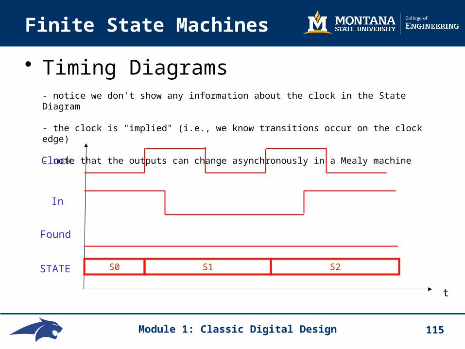
• Timing Diagrams- notice we don't show any information about the clock in the State Diagram
- the clock is "implied" (i.e., we know transitions occur on the clock edge)
- note that the outputs can change asynchronously in a Mealy machine
t
Clock
In
STATE S0 S1 S2
Found

Module 1: Classic Digital Design 116
Finite State Machines
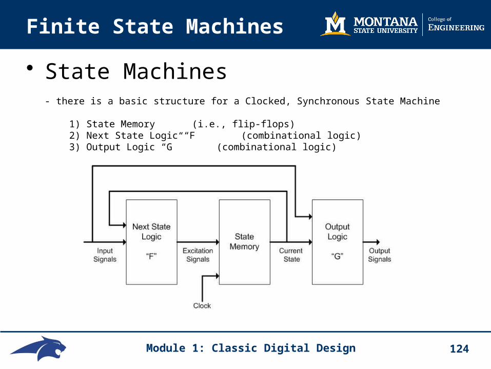
• State Machines- there is a basic structure for a Clocked, Synchronous State Machine
1) State Memory (i.e., flip-flops) 2) Next State Logic “F” (combinational logic) 3) Output Logic “G” (combinational logic)

Module 1: Classic Digital Design 117
Finite State Machines
• State Machines- the steps in a state machine design are:
1) Word Description of the Problem 2) State Diagram 3) State/Output Table 4) State Variable Assignment 5) Choose Flip-Flop type 6) Construct F 7) Construct G 8) Logic Diagram

Module 1: Classic Digital Design 118
Finite State Machines
• State Machine Example “Simple Gray Code Counter”1) Design a 2-bit Gray Code Counter. There are no inputs (other than the clock). Use Binary for the State Variable Encoding
2) State Diagram

Module 1: Classic Digital Design 119
Finite State Machines
• State Machine Example “Simple Gray Code Counter”3) State/Output Table
Current State Next State Out
CNT0 CNT1 0 0
CNT1 CNT2 0 1
CNT2 CNT3 1 1
CNT3 CNT0 1 0

Module 1: Classic Digital Design 120
Finite State Machines
• State Machine Example “Simple Gray Code Counter”4) State Variable Assignment – binary
Current State Next State Out Q1 Q0 Q1* Q0*
0 0 0 1 0 0
0 1 1 0 0 1
1 0 1 1 1 1
1 1 0 0 1 0
5) Choose Flip-Flops - let's use DFF's
Module 1: Classic Digital Design 121
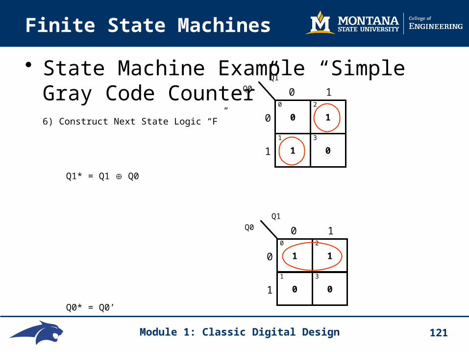
Finite State Machines
• State Machine Example “Simple Gray Code Counter”6) Construct Next State Logic “F”
Q1* = Q1 Q0
Q0* = Q0’
0 1
1 0
Q1
Q0 0 1
0
1
0
1
2
3
1 1
0 0
Q1
Q0 0 1
0
1
0
1
2
3

Module 1: Classic Digital Design 122
Finite State Machines
• State Machine Example “Simple Gray Code Counter”7) Construct Output Logic “G”
Out(1) = Q1
Out(0) = Q1 Q0
0 1
0 1
Q1
Q0 0 1
0
1
0
1
2
3
0 1
1 0
Q1
Q0 0 1
0
1
0
1
2
3
Module 1: Classic Digital Design 123
Finite State Machines
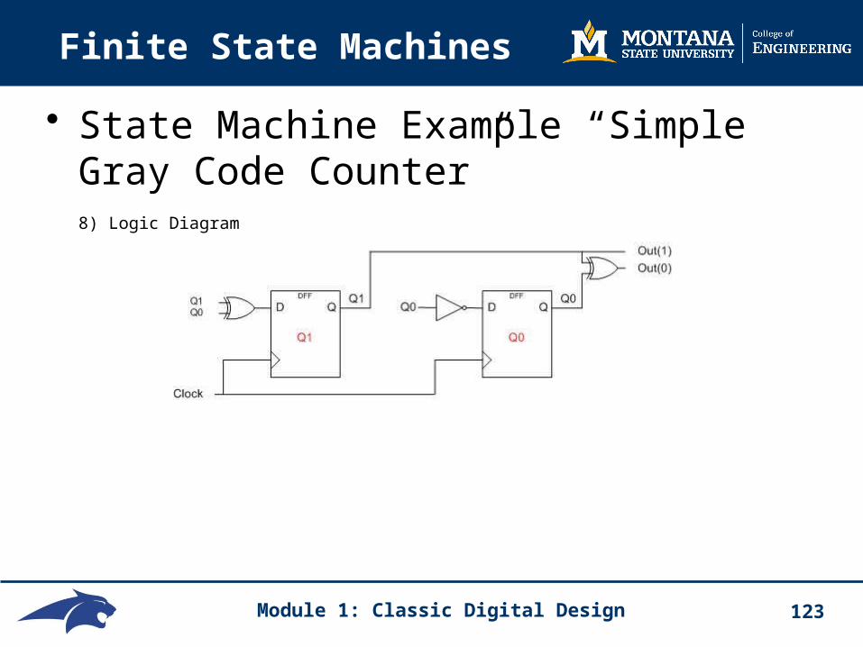
• State Machine Example “Simple Gray Code Counter”8) Logic Diagram
Module 1: Classic Digital Design 124
Finite State Machines
• State Machines- there is a basic structure for a Clocked, Synchronous State Machine
1) State Memory (i.e., flip-flops) 2) Next State Logic “F (combinational logic) 3) Output Logic “G” (combinational logic)

Module 1: Classic Digital Design 125
Finite State Machines
• State Machines- the steps in a state machine design are:
1) Word Description of the Problem 2) State Diagram 3) State/Output Table 4) State Variable Assignment 5) Choose Flip-Flop type 6) Construct F 7) Construct G 8) Logic Diagram
Module 1: Classic Digital Design 126
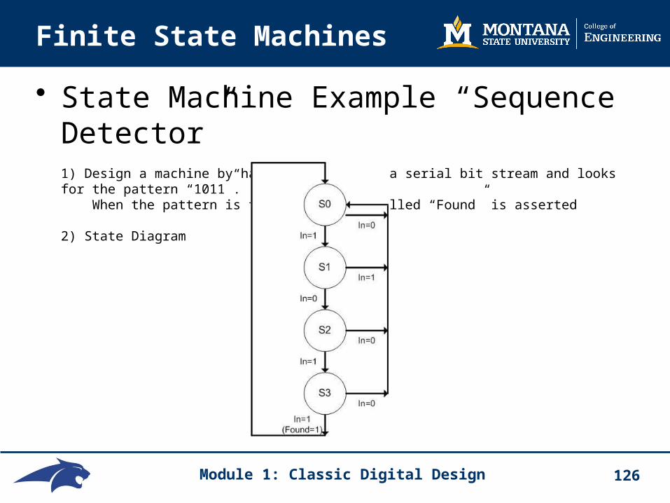
Finite State Machines
• State Machine Example “Sequence Detector”1) Design a machine by hand that takes in a serial bit stream and looks for the pattern “1011”. When the pattern is found, a signal called “Found” is asserted
2) State Diagram

Module 1: Classic Digital Design 127
Finite State Machines
• State Machine Example “Sequence Detector”3) State/Output Table
Current State In Next State Out (Found)
S0 0 S0 01 S1 0
S1 0 S2 01 S0 0
S2 0 S0 01 S3 0
S3 0 S0 01 S0 1

Module 1: Classic Digital Design 128
Finite State Machines
• State Machine Example “Sequence Detector”4) State Variable Assignment – let’s use binary
Current State In Next State Out Q1 Q0 Q1* Q0* Found
0 0 0 0 0 01 0 1 0
0 1 0 1 0 01 0 0 0
1 0 0 0 0 01 1 1 0
1 1 0 0 0 01 0 0 1
5) Choose Flip-Flop Type
- 99% of the time we use D-Flip-Flops

Module 1: Classic Digital Design 129
Finite State Machines
• State Machine Example “Sequence Detector”6) Construct Next State Logic “F”
Q1* = Q1’∙Q0∙In’ + Q1∙Q0’∙In
Q0* = Q0’∙In
0 1
0 0
Q1 Q0
In 00 01
0
1
0
1
2
3
In
Q1
0
0
6
7
0
1
4
5
11 10
Q0
0 0
1 0
Q1 Q0
In 00 01
0
1
0
1
2
3
In
Q1
0
0
6
7
0
1
4
5
11 10
Q0
Module 1: Classic Digital Design 130
Finite State Machines
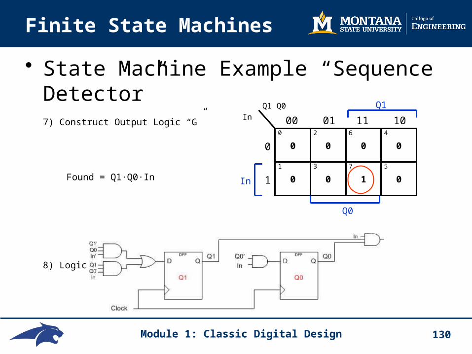
• State Machine Example “Sequence Detector”7) Construct Output Logic “G”
Found = Q1∙Q0∙In
8) Logic Diagram
0 0
0 0
Q1 Q0
In 00 01
0
1
0
1
2
3
In
Q1
0
1
6
7
0
0
4
5
11 10
Q0
Module 1: Classic Digital Design 131
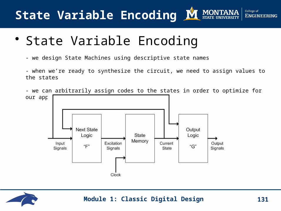
State Variable Encoding
• State Variable Encoding- we design State Machines using descriptive state names
- when we’re ready to synthesize the circuit, we need to assign values to the states
- we can arbitrarily assign codes to the states in order to optimize for our application
Module 1: Classic Digital Design 132
State Variable Encoding
• Binary- this is the simplest and most straight forward method
- we simply assign binary counts to the states
S0 = 00 S1 = 01 S2 = 10 S3 = 11
- for N states, there will be log(N)/log(2) flip flops required to encode in binary
- the advantages to Binary State Encoding are:
1) Efficient use of area (i.e., least amount of Flip-flops) - the disadvantages are:
1) Multiple bits switch at one time leading to increased Noise and Power 2) The next state logic can be multi-level which decreases speed

Module 1: Classic Digital Design 133
State Variable Encoding
• Gray Code- to avoid multiple bits switching, we can use a Gray Code
S0 = 00 S1 = 01 S2 = 11 S3 = 10
- for N states, there will be log(N)/log(2) flip flops required
- the advantages of Gray Code Encoding are:
1) One-bit switching at a time which reduces Noise/Power
- the disadvantages are:
1) Unless doing a counter, it is hard to guarantee the order of state execution 2) The next state logic can again be multi-level which decreases speed

Module 1: Classic Digital Design 134
State Variable Encoding
• One-Hot- this encoding technique uses one flip-flop for each state.
- each flip-flop asserts when in its assigned state
S0 = 0001 S1 = 0010 S2 = 0100 S3 = 1000
- for N states, there will be N flip flops required
- the advantages of One-Hot Encoding are:
1) Speed, the next state logic is one level (i.e., a Decoder structure) 2) Suited well for FPGA’s which have LUT’s & FF’s in each Cell
- the disadvantages are:
1) Takes more area

Module 1: Classic Digital Design 135
State Machine Example: Design a 2-bit Gray Code Counter with “State Encoded Outputs”
Sequential Logic
00
01
11
10
1) Number of States? : 4
2) Number of bits to encode states? : 2n=4, n=2
3) Moore or Mealy? : Moore
For this counter, we can make the outputs be the state codes

Module 1: Classic Digital Design 136
State Machine Example: Design a 2-bit Gray Code Counter
Sequential Logic
00
01
11
10
STATE
Current Next
Acur Bcur Anxt Bnxt
0 0 0 1
0 1 1 1
1 1 1 0
1 0 0 0
0 1
0 1
Bcur 0 1
Acur 0 1
Anxt Logic
Anxt = Bcur
1 1
0 0
Bcur 0 1
Acur 0 1
Bnxt Logic
Bnxt = Acur’
D Q
Q
D Q
Q
A B
CLK
A
Bcounteroutput