EE241 Advanced Digital Integrated Circuits Spring 2013...
7
EE241 Advanced Digital Integrated Circuits Spring 2013. HOMEWORK 2 SOLUTIONS 1. Extracting and simulating the synthesized design. In the first lab, we have created a design by using a strictly digital (‘VLSI’) design flow. In this assignment, we will extract the synthesized and automatically placed and routed design to look under its hood. We will compare the results of dynamic simulation to the static timing analysis. To do this, please work through the tutorial entitled: Using VLSI Flow Outputs, then turn in: a) For the path A[2] rise to Z[15] rise, report the delay measured by IC Compiler, SPICE simulated without extracted parasitics, and SPICE simulated with parasitics b) A screenshot of the critical path highlighted in IC Compiler showing the wires that contribute to the path from a) c) For the functional testbench that counts from A=0000 to A=1111, report the power measured by Primetime, the SPICE simulation, and the mixed-signal simulation. d) Run the mixed-mode simulation at 1.05V, 0.8V, 0.6V, and 0.4V and measure the average power at each point. Then convert average power to energy/op in terms of J/op and uW/Mhz. Compare these results from the theoretically predicted active energy savings for voltage scaling based on the 1.05V result and discuss possible reasons for the discrepency (Hint: think about leakage). Note that you will need to increase the clock period of the simulation for lower supply voltages. Make a reasonable assumption: you can either run a simulation to find the FO4 at different voltages to scale appropriately, or use trial and error to set a clock period that still yields correct results in the simulation output. Solution (contributed by Pi-Feng Chiu) a) For the path A[2] rise to Z[15] rise, • Delay report by ICC: actual arrival time – 88.74ps • SPICE result
Transcript of EE241 Advanced Digital Integrated Circuits Spring 2013...

EE241 Advanced Digital Integrated Circuits Spring 2013. HOMEWORK 2 SOLUTIONS 1. Extracting and simulating the synthesized design. In the first lab, we have created a design by using a strictly digital (‘VLSI’) design flow. In this assignment, we will extract the synthesized and automatically placed and routed design to look under its hood. We will compare the results of dynamic simulation to the static timing analysis. To do this, please work through the tutorial entitled: Using VLSI Flow Outputs, then turn in: a) For the path A[2] rise to Z[15] rise, report the delay measured by IC Compiler, SPICE simulated without extracted parasitics, and SPICE simulated with parasitics b) A screenshot of the critical path highlighted in IC Compiler showing the wires that contribute to the path from a) c) For the functional testbench that counts from A=0000 to A=1111, report the power measured by Primetime, the SPICE simulation, and the mixed-signal simulation. d) Run the mixed-mode simulation at 1.05V, 0.8V, 0.6V, and 0.4V and measure the average power at each point. Then convert average power to energy/op in terms of J/op and uW/Mhz. Compare these results from the theoretically predicted active energy savings for voltage scaling based on the 1.05V result and discuss possible reasons for the discrepency (Hint: think about leakage). Note that you will need to increase the clock period of the simulation for lower supply voltages. Make a reasonable assumption: you can either run a simulation to find the FO4 at different voltages to scale appropriately, or use trial and error to set a clock period that still yields correct results in the simulation output. Solution (contributed by Pi-Feng Chiu) a) For the path A[2] rise to Z[15] rise,
• Delay report by ICC: actual arrival time – 88.74ps
• SPICE result

without extracted parasitics: with extracted parasitics:
25.3ps 45.5ps
b) A screenshot of the critical path highlighted in IC Compiler showing the wires that contribute to the path from a)
Schematic
Layout
���������������������� ������������������������
����������������
���������������
�����������������
�� !�"�
�� !�"�
�� !�"�
�� !�"�
��#!��"�
��#!�$"�
��#!��"�
��#!��"�
��#!��"�
��#!��"�
��#!�"�
��#!%"�
��#!�"�
��#!�"�
��#!�"�
��#!$"�
��#!�"�
��#!�"�
��#!�"�
��#!�"�
����
��&�'
(���
���
���
��
���
���
)��� ���
�����&��'
����� $���� $���� ����� ����� ����� �����
�*����������
�+������
����������
,��������
+����-�.
,� ��������
���������������������� ������������������������
����������������
����������������������������������
� !"�#�
� !"�#�
� !"�#�
� !"�#�
� $"��#�
� $"��#�
� $"��#�
� $"��#�
� $"��#�
� $"��#�
� $"�#�
� $"�#�
� $"%#�
� $"�#�
� $"�#�
� $"�#�
� $"�#�
� $"�#�
� $"�#�
� $"�#�
��&
�'
(���
���
���
��
�%�
���
����)��� ���
����� %���������
�����&��'
����� ����� ����� ����� �����
�*�������������
�+������
�������� �
,��������
+����-�.
,� ��������
�������������
��
�
��
�
�� �
������� ������
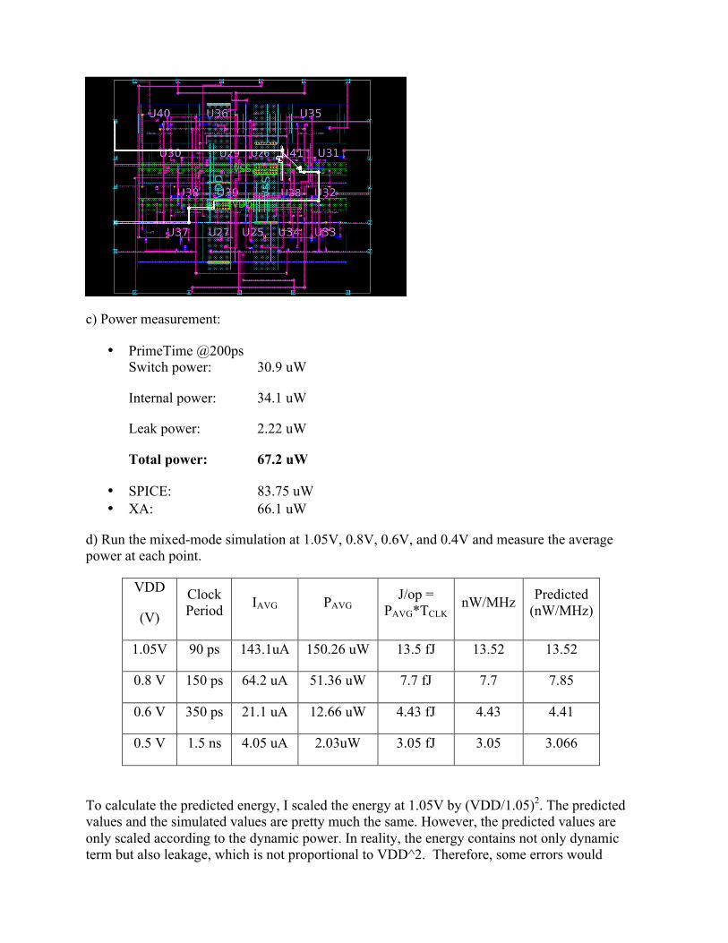
c) Power measurement:
• PrimeTime @200ps Switch power: 30.9 uW
Internal power: 34.1 uW
Leak power: 2.22 uW
Total power: 67.2 uW
• SPICE: 83.75 uW • XA: 66.1 uW
d) Run the mixed-mode simulation at 1.05V, 0.8V, 0.6V, and 0.4V and measure the average power at each point.
VDD
(V) Clock Period IAVG PAVG J/op =
PAVG*TCLK nW/MHz Predicted (nW/MHz)
1.05V 90 ps 143.1uA 150.26 uW 13.5 fJ 13.52 13.52
0.8 V 150 ps 64.2 uA 51.36 uW 7.7 fJ 7.7 7.85
0.6 V 350 ps 21.1 uA 12.66 uW 4.43 fJ 4.43 4.41
0.5 V 1.5 ns 4.05 uA 2.03uW 3.05 fJ 3.05 3.066
To calculate the predicted energy, I scaled the energy at 1.05V by (VDD/1.05)2. The predicted values and the simulated values are pretty much the same. However, the predicted values are only scaled according to the dynamic power. In reality, the energy contains not only dynamic term but also leakage, which is not proportional to VDD^2. Therefore, some errors would

results from inappropriate scaling the leakage by VDD^2.
2. SRAM redundancy and ECC We would like to investigate impact of variations on SRAM yield. Assume that read and write margins for the cells vary as Gaussian random variables with an average value of µ and a standard deviation of s. The large array that needs to be put together consists of subarrays with 256 columns and 64 rows. a) We would like to design a 12MByte array with no redundancy and a 90% yield. What should be the value of µ/s for each of the cells to achieve this yield? b) What is the µ/s for the sense amplifiers needed to attain this yield? You can assume that cell and sense amp failures are independent. c) What amount of redundancy (as a percentage of columns added per array) is needed to improve the parametric yield to 95% when designing an array from a)? Redundant columns are enabled through fuses during chip testing. d) For comparison purposes, design an error correction code (may want to search some literature) that corrects for one error per wordline and detects two errors. What is the overhead of such a scheme? If error correction is being used instead of redundancy to correct for bit faults, and applied on the original design with a 90% yield what would be the final yield? Solution (contributed by Bonjern Yang) a) For the cells to work, we need to make sure that there exists read/write margin. If X is the read/write margin for an individual cell, then the probability of a single cell working is:
𝑝! = 𝑃 𝑋 ≥ 0 = 𝑃𝑋 − 𝜇𝜎 ≥ −
𝜇𝜎 = 𝑃
𝑋 − 𝜇𝜎 ≤
𝜇𝜎 = Φ
𝜇𝜎
The third equivalency is due to the fact that X has a Gaussian distribution, which is symmetric. Φ 𝑥 is the CDF of a Gaussian distribution, with x the number of sigmas away from the mean. Knowing the probability of a single cell working, as well as the fact that each cell is independent, we can calculate the probability of the entire array working. 𝑝! = 𝑃 𝑎𝑙𝑙 𝑐𝑒𝑙𝑙𝑠 𝑤𝑜𝑟𝑘 = 𝑝!
!!"##$ For a 12 MByte array, we have 𝑁!"##$ = 12 ∗ 8 ∗ 2!". From here, we can plug in the value of ps and solve for !
!. With pt = 0.9, we get

𝑝! = Φ𝜇𝜎
!!"##$
𝜇𝜎 = Φ!! 𝑝!
!!!"##$ = 5.9904 ≈ 6
Therefore, we need !
!= 6 in order to have 90% yield.
b) First, we need to calculate the number of sense amplifiers, which is the same as the number of columns. Since we know the SRAM is composed of 256 x 64 sub-blocks, we can get the total number of columns by dividing by the number of rows.
𝑁!"#$ =𝑁!"##$
𝑁!"#$,!"#$%=12 ∗ 8 ∗ 2!"
64 = 1,572,864
Assuming the sense amplifiers have the same statistics as an individual cell and fail in a similar manner, then we can do the same calculation as in part a), but with Ncols instead of Ncells. 𝜇𝜎 = Φ!! 𝑝!
!!!"#$ = 5.273
c) For this problem, we’ll look at each sub-block, as the smallest number of extra columns we’ll want to add will be 1 to each sub-block. This is because we want to preserve uniformity in the layout. First, we should calculate the probability of a single column working. Since each cell is independent, and we had !
!= 6, this is
𝑝!,!"# = 𝑝!
!!"#$ = Φ 6 !" Since failures are independent, they are also independent between columns. Let Xn be an indicator variable of if the nth column in a sub block works. If we have k redundant columns, we have Ncols + k columns per block. Then, if Y is the number of working columns in each sub-block, the probability that a sub-block works is 𝑝!,!"#$% = 𝑃 𝑌 ≥ 𝑁!"#$ = 1− 𝑃 𝑌 < 𝑁!"#$ Since each column is independent, each Xn is an independent Bernoulli random variable, so Y is a binomial random variable, with n = Ncols + k, and p = ps,col. Then, we can simplify ps,block. 𝑝!,!"#$% = 1− 𝑃 𝑌 < 𝑁!"#$ = 1− 𝑏𝑖𝑛𝑜𝑚𝑐𝑑𝑓(𝑁!"#$ − 1;𝑁!"#$ + 𝑘,𝑝!,!"#) The total probability of the array working is the probability that all sub-blocks work. Sub-block failures are independent given the same reasoning as to why column failures are independent. Then, the total probability of success should be the products of the probability of each sub-block working. . 95 = 𝑝!,!"!,!"#$ ≤ 𝑝!,!"! = 𝑝!,!"#$%
!!"#$%&

𝑁!"#$%& =𝑁!"##$
𝑁!"#$,!"#$% ∗ 𝑁!"#$,!"#$%=12 ∗ 8 ∗ 2!"
64 ∗ 256 = 6144
𝑝!,!"!,!"#$!
!!"#$%& ≤ 𝑝!,!"#$% = 1− 𝑏𝑖𝑛𝑜𝑚𝑐𝑑𝑓 𝑁!"#$ − 1;𝑁!"#$ + 𝑘,𝑝!,!"# From here, we can sweep k until we find the first value which gives us our desired yield. We find that with even just k =1, we end up getting a yield of
𝑝!,!"! = 1− 𝑏𝑖𝑛𝑜𝑚𝑐𝑑𝑓 255; 257,𝑝!,!"#!!"#$%&
≈ .9999992 As seen, even with k = 1, we already have a yield of 99.99992%, which is higher than our 95% goal. Then, we can add 1 additional column to hit our desired yield. This is about an extra .4% of the number of columns on top on the base number. d) A code whichf can detect correct one error and detect two errors is the extended Hamming code. In this scheme, every bit position in a position of a power of 2, counting from 1, is a parity check bit. The ith parity takes the xor of 2i consecutive bits, starting from the parity bit itself, then skips the next 2i consecutive bits. It repeats this until it reaches the end of the bitstring. For this, we’ll use a coded message that has 256 bits, which maps to 247 bits of data and 9 parity check bits. If we have a bitstring of b0b1b2….b255b255, then for example, the first several parity bits are computed as 𝑝! = 𝑏! = 𝑏!⊕ 𝑏!⊕ 𝑏!⊕…⊕ 𝑏!"# 𝑝! = 𝑏! = 𝑏!⊕ 𝑏!⊕ 𝑏!⊕ 𝑏!⊕…⊕ 𝑏!"#⊕ 𝑏!"# 𝑝! = 𝑏! = 𝑏!⊕ 𝑏!⊕ 𝑏!⊕ 𝑏!⊕ 𝑏!!⊕ 𝑏!"⊕ 𝑏!"⊕ 𝑏!"⊕… 𝑝! = 𝑏! = 𝑏!⊕ 𝑏!⊕…⊕ 𝑏!"⊕ 𝑏!"⊕ 𝑏!"⊕ 𝑏!"⊕…⊕ 𝑏!"⊕ 𝑏!"⊕… This pattern continues for p4, p5, p6, p7, p8. For p9 = b255, we set this to be the xor of all other bits (from 0 through 254). We use this last bit to see if we have an error – if the parity does not match, we can use the sum of the position bit values to figure out the position of a flipped bit. The overhead of this scheme is that we use 9 bits (columns in each sub-block) for parity check, which is 3.5% of the number of columns (and cells overall). There is also additional overhead in logic which computes the parity for writing into the cells corresponding to parity bits, as well as additional logic to do error checking which has to operate on the entire 256 bit output. Given this scheme, we can calculate the overall yield by first calculating the probability of a single row in a sub-block working. If each cell in a row is independent, then the number of working cells in a row (denoted by Y) has a binomial distribution. A row works if 0 or 1 cells fail. Then: 𝑝!,!"# = 𝑃 𝑌 ≥ 𝑁!"#$ − 1 = 𝑝!,!"# = 𝑏𝑖𝑛𝑜𝑚𝑝𝑚𝑓(𝑁!"#$ − 1;𝑁!"#$,Φ(6)))+ 𝑏𝑖𝑛𝑜𝑚𝑝𝑚𝑓(𝑁!"#$;𝑁!"#$,Φ(6)) ]

An entire sub-block works if all rows work, and the entire array works if each sub-block works, so the probability of each of these is: 𝑝!,!"#$% = 𝑝!,!"#
!!"#$ 𝑝!,!"! = 𝑝!,!"#$%
!!"#$%& = 𝑝!,!"#!!"#$∗!!"#$%&
Plugging everything in, we get: 𝑝!,!"! = .9999999875 = 99.99999875% So we have a 99.99999875% yield if we use this scheme.