EE 330 Lab 1 F20 - Iowa State University
21
EE 330 Laboratory 1 Cadence Schematic Capture and Simulation Fall 2020 Contents Background Information ............................................................................................................................... 2 Checkpoints ................................................................................................................................................... 2 Part 1: Attaching Libraries ............................................................................................................................ 3 Part 2: Cell Creation ...................................................................................................................................... 3 Part 3: Schematic Capture ............................................................................................................................. 4 Instantiating the components ..................................................................................................................... 5 Connecting the components ...................................................................................................................... 6 Adding labels............................................................................................................................................. 6 Editing object properties ........................................................................................................................... 7 Adding comments ..................................................................................................................................... 8 Part 4: Circuit Simulation.............................................................................................................................. 9 DC Simulation Setup............................................................................................................................... 10 Transient Simulation Setup ..................................................................................................................... 10 AC Simulation Setup............................................................................................................................... 10 Setting up the outputs .............................................................................................................................. 11 Running the simulation and viewing the results ..................................................................................... 11 Deliverables............................................................................................................................................. 12 Part 5: ModelSim Introduction.................................................................................................................... 13 Setting up ModelSim............................................................................................................................... 13 Starting a project ..................................................................................................................................... 13 Simulating a project ................................................................................................................................ 17 Appendix A: Basic UNIX commands ......................................................................................................... 19 Appendix B: Helpful Virtuoso Hotkeys ...................................................................................................... 21
Transcript of EE 330 Lab 1 F20 - Iowa State University
EE 330 Laboratory 1
Cadence Schematic Capture and Simulation
Fall 2020
Contents Background Information ............................................................................................................................... 2
Checkpoints ................................................................................................................................................... 2
Part 1: Attaching Libraries ............................................................................................................................ 3
Part 2: Cell Creation ...................................................................................................................................... 3
Part 3: Schematic Capture ............................................................................................................................. 4
Instantiating the components ..................................................................................................................... 5
Connecting the components ...................................................................................................................... 6
Adding labels ............................................................................................................................................. 6
Editing object properties ........................................................................................................................... 7
Adding comments ..................................................................................................................................... 8
Part 4: Circuit Simulation .............................................................................................................................. 9
DC Simulation Setup ............................................................................................................................... 10
Transient Simulation Setup ..................................................................................................................... 10
AC Simulation Setup ............................................................................................................................... 10
Setting up the outputs .............................................................................................................................. 11
Running the simulation and viewing the results ..................................................................................... 11
Deliverables ............................................................................................................................................. 12
Part 5: ModelSim Introduction .................................................................................................................... 13
Setting up ModelSim ............................................................................................................................... 13
Starting a project ..................................................................................................................................... 13
Simulating a project ................................................................................................................................ 17
Appendix A: Basic UNIX commands ......................................................................................................... 19
Appendix B: Helpful Virtuoso Hotkeys ...................................................................................................... 21
Background Information In the previous lab, you gained access to the Linux environment and the Virtuoso tools you will need for future labs. This week, the purpose is to go through some basic operations and examples in Virtuoso in an attempt to gain familiarity. While the end result may not be very exciting, the content learned today will be the fundamental building blocks to using the software. Eventually, by the end of the course, you will be able to be assigned a larger and more challenging project and be able to work on it confidently.
The main parts for this lab will be placing components and getting familiar with the Virtuoso’s layout and tools. Beyond this, you will gain the ability to simulate your circuits and run them through different tests while graphing your results. Additionally, we will give you an introduction to ModelSim, which is a Hardware Design Language (HDL) simulation software which we will use in this class to simulate digital circuits.
As the semester continues, the labs will be less descriptive on processes that you should already know how to do. For example, we will no longer be telling you to launch the Linux VDI and navigate to your “ee330” folder before launching Virtuoso, instead just mentioning that you should launch Virtuoso. To extend this notion from this lab to future lab, in this lab you will learn how to set up simulations and obtain graphs and results, but future labs will just mention including the results in your report.
Checkpoints The checkpoints for this lab are as follows:
1. DC Testbench Results 2. AC Testbench Results 3. Transient Testbench Results 4. ModelSim Waveform
As with all future labs, these checkpoints must be shown to a lab TA before the end of your next lab section. You should include these checkpoints in your lab report.
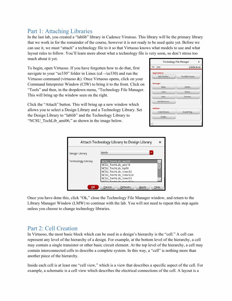
Part 1: Attaching Libraries In the last lab, you created a “lablib” library in Cadence Virutoso. This library will be the primary library that we work in for the remainder of the course, however it is not ready to be used quite yet. Before we can use it, we must “attach” a technology file to it so that Virtuoso knows what models to use and what layout rules to follow. You’ll learn more about what a technology file is very soon, so don’t stress too much about it yet.
To begin, open Virtuoso. If you have forgotten how to do that, first navigate to your “ee330” folder in Linux (cd ~/ee330) and run the Virtuoso command (virtuoso &). Once Virtuoso opens, click on your Command Interpreter Window (CIW) to bring it to the front. Click on “Tools” and then, in the dropdown menu, “Technology File Manager. This will bring up the window seen on the right.
Click the “Attach” button. This will bring up a new window which allows you to select a Design Library and a Technology Library. Set the Design Library to “lablib” and the Technology Library to “NCSU_TechLib_ami06,” as shown in the image below.
Once you have done this, click “Ok,” close the Technology File Manager window, and return to the Library Manager Window (LMW) to continue with the lab. You will not need to repeat this step again unless you choose to change technology libraries.
Part 2: Cell Creation In Virtuoso, the most basic block which can be used in a design’s hierarchy is the “cell.” A cell can represent any level of the hierarchy of a design. For example, at the bottom level of the hierarchy, a cell may contain a single transistor or other basic circuit element. At the top level of the hierarchy, a cell may contain interconnected cells to describe a complete system. In this way, a “cell” is nothing more than another piece of the hierarchy.
Inside each cell is at least one “cell view,” which is a view that describes a specific aspect of the cell. For example, a schematic is a cell view which describes the electrical connections of the cell. A layout is a
cell view which describes the physical placement and routing of the items contained within the cell. A symbol is a cell view which describes the way that the cell will be graphically represented if used in other cells. If you don’t fully understand this yet, that’s OK; you’ll gain familiarity with cells and cell views as you use them in lab.
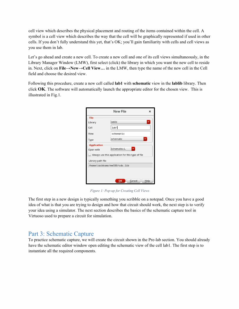
Let’s go ahead and create a new cell. To create a new cell and one of its cell views simultaneously, in the Library Manager Window (LMW), first select (click) the library in which you want the new cell to reside in. Next, click on File→New→Cell View… in the LMW, then type the name of the new cell in the Cell field and choose the desired view.
Following this procedure, create a new cell called lab1 with schematic view in the lablib library. Then click OK. The software will automatically launch the appropriate editor for the chosen view. This is illustrated in Fig.1.
Figure 1: Pop-up for Creating Cell Views
The first step in a new design is typically something you scribble on a notepad. Once you have a good idea of what is that you are trying to design and how that circuit should work, the next step is to verify your idea using a simulator. The next section describes the basics of the schematic capture tool in Virtuoso used to prepare a circuit for simulation.
Part 3: Schematic Capture To practice schematic capture, we will create the circuit shown in the Pre-lab section. You should already have the schematic editor window open editing the schematic view of the cell lab1. The first step is to instantiate all the required components.
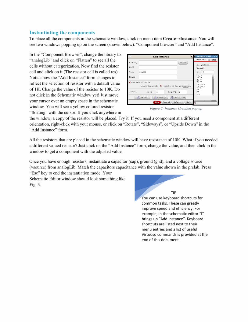
Instantiating the components To place all the components in the schematic window, click on menu item Create→Instance. You will see two windows popping up on the screen (shown below): “Component browser” and “Add Instance”.
In the “Component Browser”, change the library to “analogLib” and click on “Flatten” to see all the cells without categorization. Now find the resistor cell and click on it (The resistor cell is called res). Notice how the “Add Instance” form changes to reflect the selection of resistor with a default value of 1K. Change the value of the resistor to 10K. Do not click in the Schematic window yet! Just move your cursor over an empty space in the schematic window. You will see a yellow colored resistor “floating” with the cursor. If you click anywhere in the window, a copy of the resistor will be placed. Try it. If you need a component at a different orientation, right-click with your mouse, or click on “Rotate”, “Sideways”, or “Upside Down” in the “Add Instance” form.
All the resistors that are placed in the schematic window will have resistance of 10K. What if you needed a different valued resistor? Just click on the “Add Instance” form, change the value, and then click in the window to get a component with the adjusted value.
Once you have enough resistors, instantiate a capacitor (cap), ground (gnd), and a voltage source (vsource) from analogLib. Match the capacitors capacitance with the value shown in the prelab. Press “Esc” key to end the instantiation mode. Your Schematic Editor window should look something like Fig. 3.
Figure 2: Instance Creation pop-up
TIP You can use keyboard shortcuts for common tasks. These can greatly improve speed and efficiency. For example, in the schematic editor “I” brings up “Add Instance”. Keyboard shortcuts are listed next to their menu entries and a list of useful Virtuoso commands is provided at the end of this document.

Figure 3: Schematic Editor Window for cell lab1
Connecting the components There are two ways to interconnect components. First, use the menu entry Create→Wire (narrow) to get into the wiring mode (You could also have pressed the shortcut “w” key or clicked on the Add-Wire (narrow) icon). When in wiring mode, click on the red terminal of a component to start one end of the wire (you do not need to keep the button down). Now click on the other component’s terminal where you want the connection to terminate. If you make a mistake and want to quit the wiring mode, press the “Escape” key on the keyboard. You can undo the last action by pressing “u” and redo it by pressing “Shift u”.
The second way to add wiring is to first bring the mouse pointer over the red terminal of a component’s terminal. While clicking and holding the mouse button, drag you mouse, and you will see a wire started. You can let go of the button now and the wiring will continue. Hit “Escape” anytime to cancel. Unlike the first method, the wiring mode automatically terminates with the completion of one connection.
Complete wiring the circuit. To make sure there are no floating components or connection problems, we need to “Check and Save” the design. Click on the icon or the “Check and Save” entry from the “File” menu. Check the CIW window to make sure the design was saved without errors. The information outputted into the CIW may be overwhelming at first, but you are encouraged to take time to filter through it anyways. The CIW is a critical tool for debugging problems in Virtuoso.
Adding labels As you wire the components together, every net is automatically assigned a name such as net1, net2, etc. These names are fine for the software but are not easy for us to remember. Adding labels to wires helps us to interact with the tools more efficiently. To add a label to a wire, click on the menu item Create→Wire Name (or use shortcut “l”). In the form, type “vIn vMid vOut”. Bring your mouse pointer into the schematic window. If you do not see the “floating” vIn attached to your cursor, you first need to click on the title bar of the schematic window to make it active. Now you should see the vIn attached to the mouse pointer. Click your mouse pointer on the net you wish to call vIn. Note how the next label from the list you typed in the form appears once you have placed the first label. This is a

convenient way of adding multiple labels without having to go back and forth between the form and the schematic window.
Labels provide functionality in addition to being visual aids: connectivity. If two unconnected nets have the same name, they are considered to be electrically connected (this may come in handy later when connection multiple components to VDD and VSS). This feature can allow you to create schematics with less clutter but can also be a source of mistakes. Use the capability of labels to create connectivity judiciously or your schematics may actually become less readable.
Figure 4:Schematic showing interconnected components and net labels
Editing object properties What if you made a typing mistake when creating labels or need to modify the value of a component? You can make the required changes by clicking on the object which you want to change and then clicking Edit→Properties→Objects (find the shortcut for this if you don’t want to click three menu levels every time!).
For practice, let us modify the properties of the voltage source component, vsource. The vsource component is capable of generating a variety of stimuli.
Bring up the properties form for vsource. In the next section, we will run dc, ac, and transient simulations. For those simulations to work, we need to configure the vsource object to provide appropriate input stimuli.
TIP It is possible, and often preferable, to use other sources from analogLib, such as vdc for dc only and vsin for sine waves. vsource has multiple options, so it is used here to be able to switch between them easily.
DC simulation
In the “DC voltage” box, type 1. This dc voltage is used to compute the quiescent operating point of the circuit (you’ll learn more about that in the future). Click on apply (at the bottom of the form). This is the input for dc analysis.
AC analysis input
Find the entry “Display small signal params” and turn the option on. The form will update to display new form fields. Add 1V in the “AC magnitude”. This input value will be used for the AC analysis.
Transient analysis
You need to set the “Source type” field to the type you need to generate, in this case you need a step function (i.e. what options from the dropdown will get you a step function?). Instead of telling you exactly what to set it to, we’ll let you play with it so you can gain familiarity with the different source types. Once you have entered all the applicable entries, click on OK.
The vsource component is now configured for simulations. Click on “Check and save” to save your design. Correct any errors or warnings before proceeding further.
Adding comments Especially for larger designs (for example, your final project), it is good practice to add comments to the schematics. Click on Create→Note→Text… and fill out the form. The comments are useful reminders to yourself about the particular schematic and can also provide instructions for others if you share your schematics.

Part 4: Circuit Simulation Once the schematic capture is complete, we can simulate the circuit to test if it performs according to the design. To do this, we first open the Analog Design Environment (ADE) window. To open the ADE window, click on Launch→ADE L while in the schematic tool. After opening the ADE window, go to Setup → Simulator/Directory/Host and set the Project Directory path to: /local/[username]/simulation
Having your project directory set to this location will keep your simulation data stored on the /local/ rather than eating up your account space. It is also highly recommended to keep on deleting the old simulation data from time to time so that everyone can have enough /local/ space.
Once you have ensured that your project directory is correct, go to Setup → Model Libraries… and check that you see a window which looks similar to the figure below.
Make sure one of the lines in this window says “$CDK_DIR/models/spectre/standalone/ami06P.m” and one says “$CDK_DIR/models/spectre/standalone/ami06N.m”. You should have both lines in your model libraries, but if you are missing one, copy and add the missing line simply by copying the path from this lab document and pasting it into the line that says “Click here to add model file.” If you fail to do this, the ADE will not know where to obtain the model libraries from and will fail to simulate your circuit.
TIP Always click “check and save” before running a simulation. Changing anything in the schematic will make the simulation fail unless a “check and save” is run. Save often. Cadence tools have a tendency to crash, although this occurs more often for more complex designs. Using “save” instead of “check and save” will save whatever you are currently working on without a pop-up box pointing out errors and possibly not saving.

DC Simulation Setup Initiate the click sequence Analysis→Choose. This will cause the pop-up form “Choosing Analysis” to appear. We will first run a dc analysis. Click on the button next to dc in the form. The form contents will update to show entries relevant to a dc analysis. We would like to save the dc operating point and sweep the input voltage from 0 to 5 volts. To sweep the input dc voltage, we first need to select the appropriate parameter to sweep. In the “sweep variable” box area, click on the “component parameter” button. The updated form is shown on the right.
To select the dc input voltage of the vsource, click on “Select component” and then click on vsource in the schematics window. In the new form that pops up, click on the first entry, dc, to choose the dc voltage of the vsource. You would follow a similar procedure to sweep another parameter of a source, if desired.
Next, enter the range of sweep in the start and stop boxes. Click on Apply for all these changes to take effect. This completes the dc analysis setup. Click OK to close the form and return to ADE.
Transient Simulation Setup A transient analysis is nothing more than an analysis which runs for a specific amount of time. To setup a transient analysis, click Analysis→Choose and then select “tran.” Put the desired length of time that you want to run the analysis in the “Stop Time” field. It is up to you to decide how long you should run your simulation. Remember, the goal here is to prove that your results from the pre-lab are correct. Note that you can do small increments of time by typing the value and unit right by each other. For example, for 1𝜇𝑠, type “1u” into the Stop Time field. Typing “1 u”, “1u s”, or any other modification will not work.
Once you have entered the duration that you want the simulation to run for, click OK to close the form and return to the ADE. You should now have two simulations showing in the “Analyses” section in the ADE.
AC Simulation Setup An AC analysis is an analysis which plots the magnitude of a signal as the frequency of the input sinusoid changes. You can think of it as being similar to a DC sweep, but with a frequency being swept instead. It is useful for determining the frequency response of a circuit.
To setup an AC analysis, click Analysis→Choose and then select “ac.” The simulation configuration area should update and default to have the Sweep Variable set to “Frequency.” In the Sweep Range, select “Start-Stop” and choose the starting and stopping frequency for your simulation. It is not necessary to include “Hz” at the end of your frequencies. Remember that the goal of this simulation is to prove that your pre-lab work is correct. To do this, consider sweeping frequencies which are within 1𝑑𝐵 of your anticipated corner frequency and checking that signal is the expected magnitude at your corner frequency.

An example setup is provided below. This setup is defining an AC analysis which will sweep from 1𝑚𝐻𝑧 to 1𝑀𝐻𝑧. Notice that the “m” and “M” suffixes are located immediately after the number. Do not put a space between the number and the suffix. Also do not include “Hz.”
Once you have entered your desired frequency sweep, click OK to close the form and return to the ADE. You should now have three simulations showing in the “Analyses” section in the ADE.
Setting up the outputs We need to tell the simulator which node voltages we are interested in plotting once the simulation is complete. To choose which signals to plot, click on the menu item
Outputs→To be Plotted →Select on Schematics. The bottom of the ADE tells you to select the outputs you want plotted. Clicking on a net or a label selects voltage of the net to be plotted. Find the schematics window and click on the three labels we added earlier. Once done, press the escape key to get out of this selection mode. If you fail to hit the escape key, next time you enter the schematic window to change something, it will continue adding nets to your simulation.
Running the simulation and viewing the results Now that we have setup the analyses that we intend to perform and selected the outputs that we are interested in, let us run the simulation. Begin by unchecking the “Enable” option for two of the analyses that you created, just leaving one checked. Then, click on the green arrow icon to run the simulation. Cadence may take a moment to crunch the numbers, but once the simulation is complete, a waveform viewer window should come up with the plots of the outputs you selected in the previous step. Virtuoso’s waveform viewer, just like everything else with Virtuoso, is powerful. In this class, though, we’ll only use the basic tools offered in the viewer. The image below highlights a number of buttons in the viewer; below the image, a description of what each button does is provided.
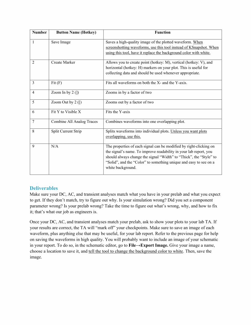
Number Button Name (Hotkey) Function
1 Save Image Saves a high-quality image of the plotted waveform. When screenshotting waveforms, use this tool instead of KSnapshot. When using this tool, have it replace the background color with white.
2 Create Marker Allows you to create point (hotkey: M), vertical (hotkey: V), and horizontal (hotkey: H) markers on your plot. This is useful for collecting data and should be used whenever appropriate.
3 Fit (F) Fits all waveforms on both the X- and the Y-axis.
4 Zoom In by 2 (]) Zooms in by a factor of two
5 Zoom Out by 2 ([) Zooms out by a factor of two
6 Fit Y to Visible X Fits the Y-axis
7 Combine All Analog Traces Combines waveforms into one overlapping plot.
8 Split Current Strip Splits waveforms into individual plots. Unless you want plots overlapping, use this.
9 N/A The properties of each signal can be modified by right-clicking on the signal’s name. To improve readability in your lab report, you should always change the signal “Width” to “Thick”, the “Style” to “Solid”, and the “Color” to something unique and easy to see on a white background.
Deliverables Make sure your DC, AC, and transient analyses match what you have in your prelab and what you expect to get. If they don’t match, try to figure out why. Is your simulation wrong? Did you set a component parameter wrong? Is your prelab wrong? Take the time to figure out what’s wrong, why, and how to fix it; that’s what our job as engineers is.
Once your DC, AC, and transient analyses match your prelab, ask to show your plots to your lab TA. If your results are correct, the TA will “mark off” your checkpoints. Make sure to save an image of each waveform, plus anything else that may be useful, for your lab report. Refer to the previous page for help on saving the waveforms in high quality. You will probably want to include an image of your schematic in your report. To do so, in the schematic editor, go to File→Export Image. Give your image a name, choose a location to save it, and tell the tool to change the background color to white. Then, save the image.
Part 5: ModelSim Introduction Setting up ModelSim Throughout this course, in addition to working on analog circuits, we will be using Verilog to simulate and design digital circuits and systems. Verilog is what is known as a hardware design language (HDL), and is one of the languages used heavily by designers doing digital VLSI to create digital circuits. The tool that we use to run Verilog code is called “ModelSim.”
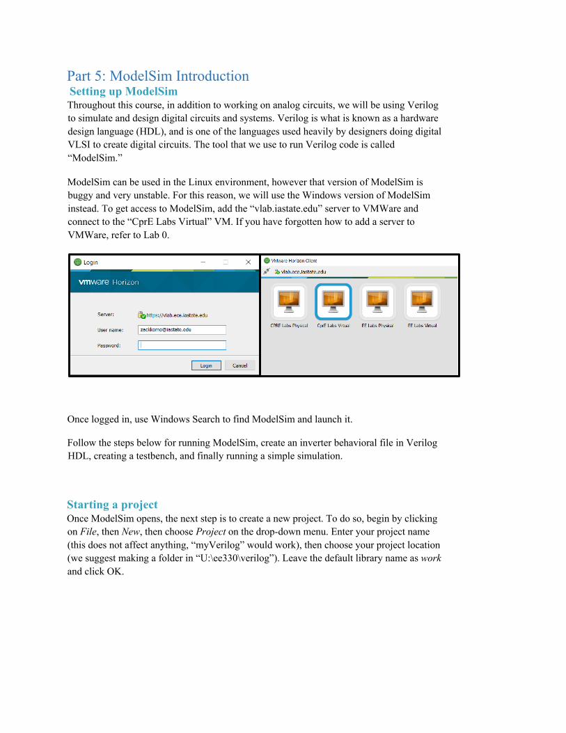
ModelSim can be used in the Linux environment, however that version of ModelSim is buggy and very unstable. For this reason, we will use the Windows version of ModelSim instead. To get access to ModelSim, add the “vlab.iastate.edu” server to VMWare and connect to the “CprE Labs Virtual” VM. If you have forgotten how to add a server to VMWare, refer to Lab 0.
Once logged in, use Windows Search to find ModelSim and launch it.
Follow the steps below for running ModelSim, create an inverter behavioral file in Verilog HDL, creating a testbench, and finally running a simple simulation.
Starting a project Once ModelSim opens, the next step is to create a new project. To do so, begin by clicking on File, then New, then choose Project on the drop-down menu. Enter your project name (this does not affect anything, “myVerilog” would work), then choose your project location (we suggest making a folder in “U:\ee330\verilog”). Leave the default library name as work and click OK.
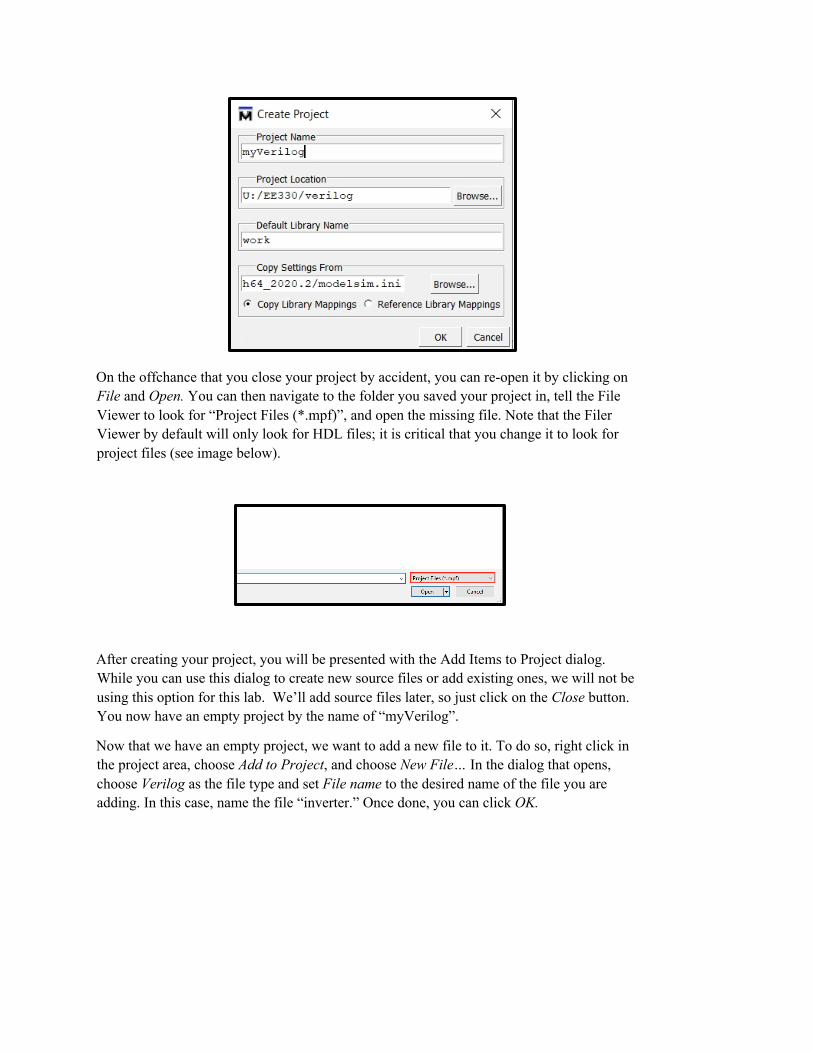
On the offchance that you close your project by accident, you can re-open it by clicking on File and Open. You can then navigate to the folder you saved your project in, tell the File Viewer to look for “Project Files (*.mpf)”, and open the missing file. Note that the Filer Viewer by default will only look for HDL files; it is critical that you change it to look for project files (see image below).
After creating your project, you will be presented with the Add Items to Project dialog. While you can use this dialog to create new source files or add existing ones, we will not be using this option for this lab. We’ll add source files later, so just click on the Close button. You now have an empty project by the name of “myVerilog”.
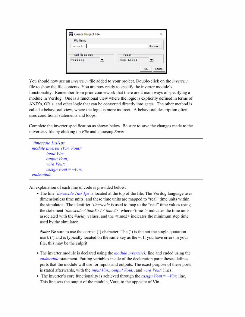
Now that we have an empty project, we want to add a new file to it. To do so, right click in the project area, choose Add to Project, and choose New File… In the dialog that opens, choose Verilog as the file type and set File name to the desired name of the file you are adding. In this case, name the file “inverter.” Once done, you can click OK.
You should now see an inverter.v file added to your project. Double-click on the inverter.v file to show the file contents. You are now ready to specify the inverter module’s functionality. Remember from prior coursework that there are 2 main ways of specifying a module in Verilog. One is a functional view where the logic is explicitly defined in terms of AND’s, OR’s, and other logic that can be converted directly into gates. The other method is called a behavioral view, where the logic is more indirect. A behavioral description often uses conditional statements and loops.
Complete the inverter specification as shown below. Be sure to save the changes made to the intverter.v file by clicking on File and choosing Save:
An explanation of each line of code is provided below: • The line `timescale 1ns/ 1ps is located at the top of the file. The Verilog language uses
dimensionless time units, and these time units are mapped to “real” time units within the simulator. The identifier `timescale is used to map to the “real” time values using the statement `timescale <time1> / <time2>, where <time1> indicates the time units associated with the #delay values, and the <time2> indicates the minimum step time used by the simulator.
Note: Be sure to use the correct (`) character. The (`) is the not the single quotation mark (‘) and is typically located on the same key as the ~. If you have errors in your file, this may be the culprit.
• The inverter module is declared using the module inverter(); line and ended using the endmodule statement. Putting variables inside of the declaration parentheses defines ports that the module will use for inputs and outputs. The exact purpose of these ports is stated afterwards, with the input Vin;, output Vout;, and wire Vout; lines.
• The inverter’s core functionality is achieved through the assign Vout = ~Vin; line. This line sets the output of the module, Vout, to the opposite of Vin.
`timescale 1ns/1ps module inverter (Vin, Vout);
input Vin; output Vout; wire Vout; assign Vout = ~Vin;
endmodule
Once we have defined the inverter specification, we need to add a testbench to validate its functionality. Essentially, with the inverter.v file we created a model such that it inverts an input. When running a simulation, though, we would have to specify what that input is. By creating a testbench function, we can have the inputs flip automatically and observe the outputs. To do so, create a new Verilog file in the myVerilog project (in the same way that you created the inverter.v file) and call it “inverter_tb.v”. Then we add the functionality of the testbench module as shown below. Note, we use the inverter function we created in inverter.v and feed it inputs that we have automatically iterate.
An explanation of each line is provided below:
• `timescale 1ns/1ps : sets how long an operation lasts. This is used later in the #20 A <= ~A line, which means every 20 timescale interval set A to equal not A.
• module [Name](Parameters); the [Name] is the actual name of the device, to be referenced by other devices. The Parameters are all inputs and outputs, things that can be accessed by other devices.
• reg A; This sets A as a register, which means it can be controlled using statements later.
• initial begin A = 1'b0; end : initial sets the initial state of things inside of it, in this case the register A being set to 0. Because A is 1 bit long A = [bits]’b[inary]0, if A were 4 bits it would be A = 4’b0000. The ‘begin’ and ‘end’ work like parenthesize in other programs, they allow multiple lines to be controlled by the ‘initial’ above.
• always #20 A <= ~A; always@(event) causes what is inside the always statement to occur when the event occurs. always@(posedge Clock) will cause whatever is in it to happen when a signal called Clock becomes positive from negative. If ‘always’ has no @ statement it happens whenever any signal changes in the code. The #20 A <= ~A means every 20 timescales A becomes not A (1→0, 0→1).
• endmodule : designates the end of the program.
Notice that the inputs of the inverter module are now defined differently. The inputs of inverter.v are given values (like applying a bias from a voltage source on a real test bench to
`timescale 1ns/1ps module inverter_tb();
reg A; wire B; inverter inv( .Vin(A), .Vout(B) ); initial begin
A = 1'b0; end always
#20 A <= ~A; endmodule
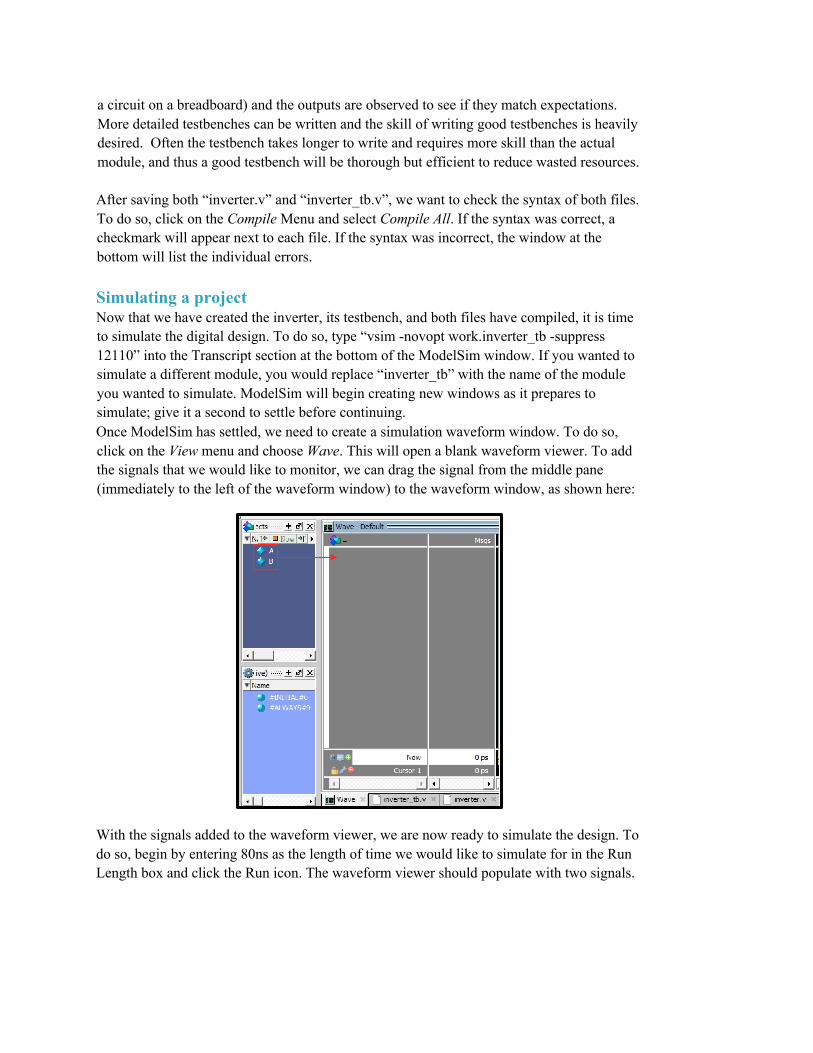
a circuit on a breadboard) and the outputs are observed to see if they match expectations. More detailed testbenches can be written and the skill of writing good testbenches is heavily desired. Often the testbench takes longer to write and requires more skill than the actual module, and thus a good testbench will be thorough but efficient to reduce wasted resources. After saving both “inverter.v” and “inverter_tb.v”, we want to check the syntax of both files. To do so, click on the Compile Menu and select Compile All. If the syntax was correct, a checkmark will appear next to each file. If the syntax was incorrect, the window at the bottom will list the individual errors. Simulating a project Now that we have created the inverter, its testbench, and both files have compiled, it is time to simulate the digital design. To do so, type “vsim -novopt work.inverter_tb -suppress 12110” into the Transcript section at the bottom of the ModelSim window. If you wanted to simulate a different module, you would replace “inverter_tb” with the name of the module you wanted to simulate. ModelSim will begin creating new windows as it prepares to simulate; give it a second to settle before continuing. Once ModelSim has settled, we need to create a simulation waveform window. To do so, click on the View menu and choose Wave. This will open a blank waveform viewer. To add the signals that we would like to monitor, we can drag the signal from the middle pane (immediately to the left of the waveform window) to the waveform window, as shown here:
With the signals added to the waveform viewer, we are now ready to simulate the design. To do so, begin by entering 80ns as the length of time we would like to simulate for in the Run Length box and click the Run icon. The waveform viewer should populate with two signals.
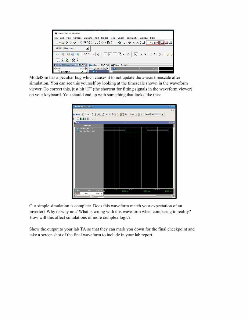
ModelSim has a peculiar bug which causes it to not update the x-axis timescale after simulation. You can see this yourself by looking at the timescale shown in the waveform viewer. To correct this, just hit “F” (the shortcut for fitting signals in the waveform viewer) on your keyboard. You should end up with something that looks like this:
Our simple simulation is complete. Does this waveform match your expectation of an inverter? Why or why not? What is wrong with this waveform when comparing to reality? How will this affect simulations of more complex logic?
Show the output to your lab TA so that they can mark you down for the final checkpoint and take a screen shot of the final waveform to include in your lab report.
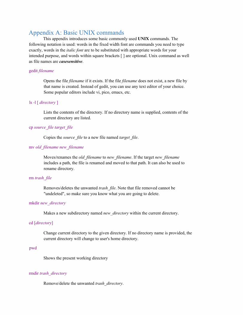
Appendix A: Basic UNIX commands This appendix introduces some basic commonly used UNIX commands. The
following notation is used: words in the fixed width font are commands you need to type exactly, words in the italic font are to be substituted with appropriate words for your intended purpose, and words within square brackets [ ] are optional. Unix command as well as file names are casesensitive.
gedit filename
Opens the file filename if it exists. If the file filename does not exist, a new file by that name is created. Instead of gedit, you can use any text editor of your choice. Some popular editors include vi, pico, emacs, etc.
ls -l [ directory ]
Lists the contents of the directory. If no directory name is supplied, contents of the current directory are listed.
cp source_file target_file
Copies the source_file to a new file named target_file.
mv old_filename new_filename
Moves/renames the old_filename to new_filename. If the target new_filename includes a path, the file is renamed and moved to that path. It can also be used to rename directory.
rm trash_file
Removes/deletes the unwanted trash_file. Note that file removed cannot be "undeleted", so make sure you know what you are going to delete.
mkdir new_directory
Makes a new subdirectory named new_directory within the current directory.
cd [directory]
Change current directory to the given directory. If no directory name is provided, the current directory will change to user's home directory.
pwd
Shows the present working directory
rmdir trash_directory
Remove/delete the unwanted trash_directory.

man command
Show the manual of the command. You can learn more detail about any given command
using man, e.g. man ls shows all available options and functionalities for ls command.
more filename
Shows the contents of a file one screen at a time.
ps
Shows the currently running processes.
A couple of useful special symbols
~
The symbol ~ is used to denote the user’s home directory. If the complete path of the home directory happens to be / home/username/ , then using ~ represents that complete string. For example, if you want to look at the contents of a file in your home directory, the following commands produce the same result
more /home/username/myfile more ~/myfile
&
When launching a program that opens in a new window, placing an “&” at the end of the command line allows the user to keep access to the command line, i.e., the “&” instructs the program to run in the background.
These are just a few shell commands you need to know to get started. You are encouraged and advised to learn other UNIX commands on your own, as they will increase your productivity, i.e., more you know, more efficient you will be.
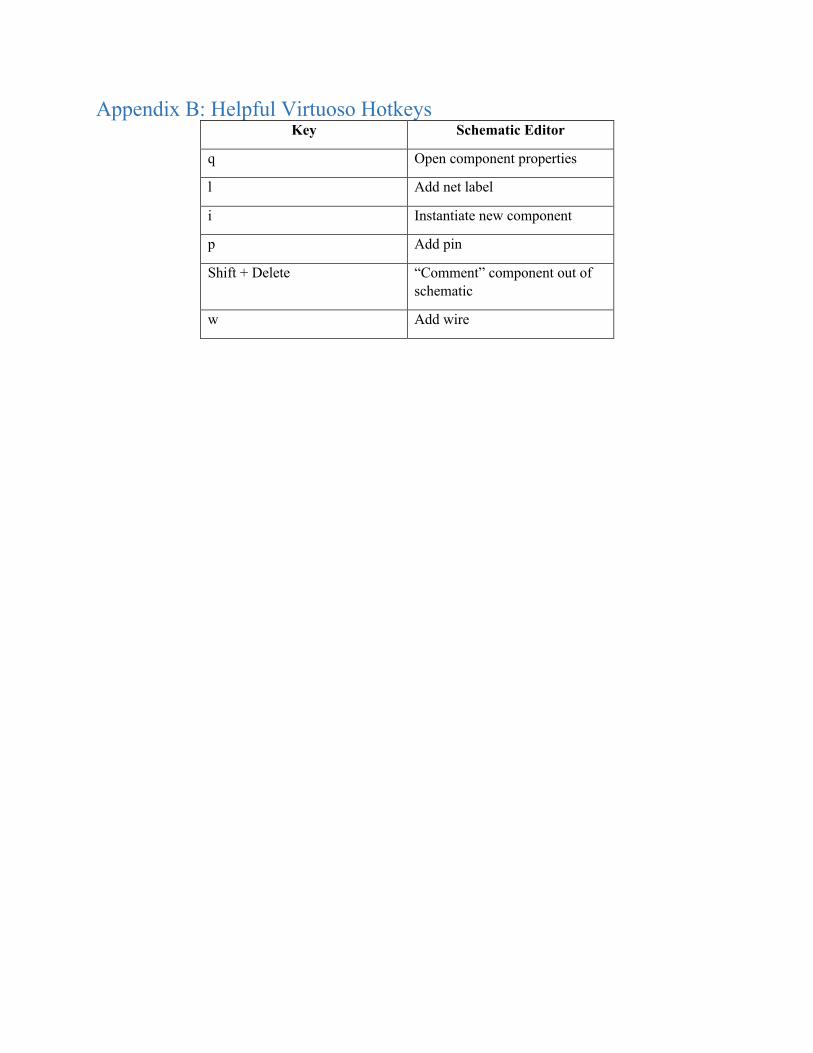
Appendix B: Helpful Virtuoso Hotkeys Key Schematic Editor
q Open component properties
l Add net label
i Instantiate new component
p Add pin
Shift + Delete “Comment” component out of schematic
w Add wire
![EE 330 Lecture 42 - Iowa State Universityclass.ece.iastate.edu/ee330/lectures/EE 330 Lect 42 Fall 2016.pdf · EE 330 Lecture 42 Digital Circuits • Elmore Delay ... Elmore delay[1]](https://static.fdocuments.us/doc/165x107/5b57fe847f8b9a4e1b8b664d/ee-330-lecture-42-iowa-state-330-lect-42-fall-2016pdf-ee-330-lecture-42-digital.jpg)