ECE5461: Low Power SoC Designcontents.kocw.net/KOCW/document/2014/sungkyunkwan/hanta... ·...
22
ECE5461: Low Power SoC Design Tae Hee Han: [email protected] Semiconductor Systems Engineering Sungkyunkwan University
Transcript of ECE5461: Low Power SoC Designcontents.kocw.net/KOCW/document/2014/sungkyunkwan/hanta... ·...

ECE5461:Low Power SoC Design
Tae Hee Han: [email protected]
Semiconductor Systems Engineering
Sungkyunkwan University

Low Power EDA Technologies
2
Low Leakage Design(Sequence Design:
Now, a part of Apache Design Solutions)
3/36
4
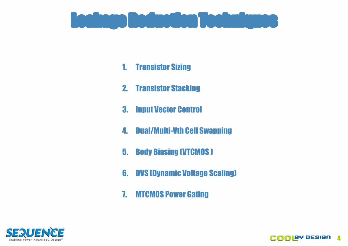
Leakage Reduction TechniquesLeakage Reduction Techniques
1. Transistor Sizing
2. Transistor Stacking
3. Input Vector Control
4. Dual/Multi-Vth Cell Swapping
5. Body Biasing (VTCMOS )
6. DVS (Dynamic Voltage Scaling)
7. MTCMOS Power Gating
5
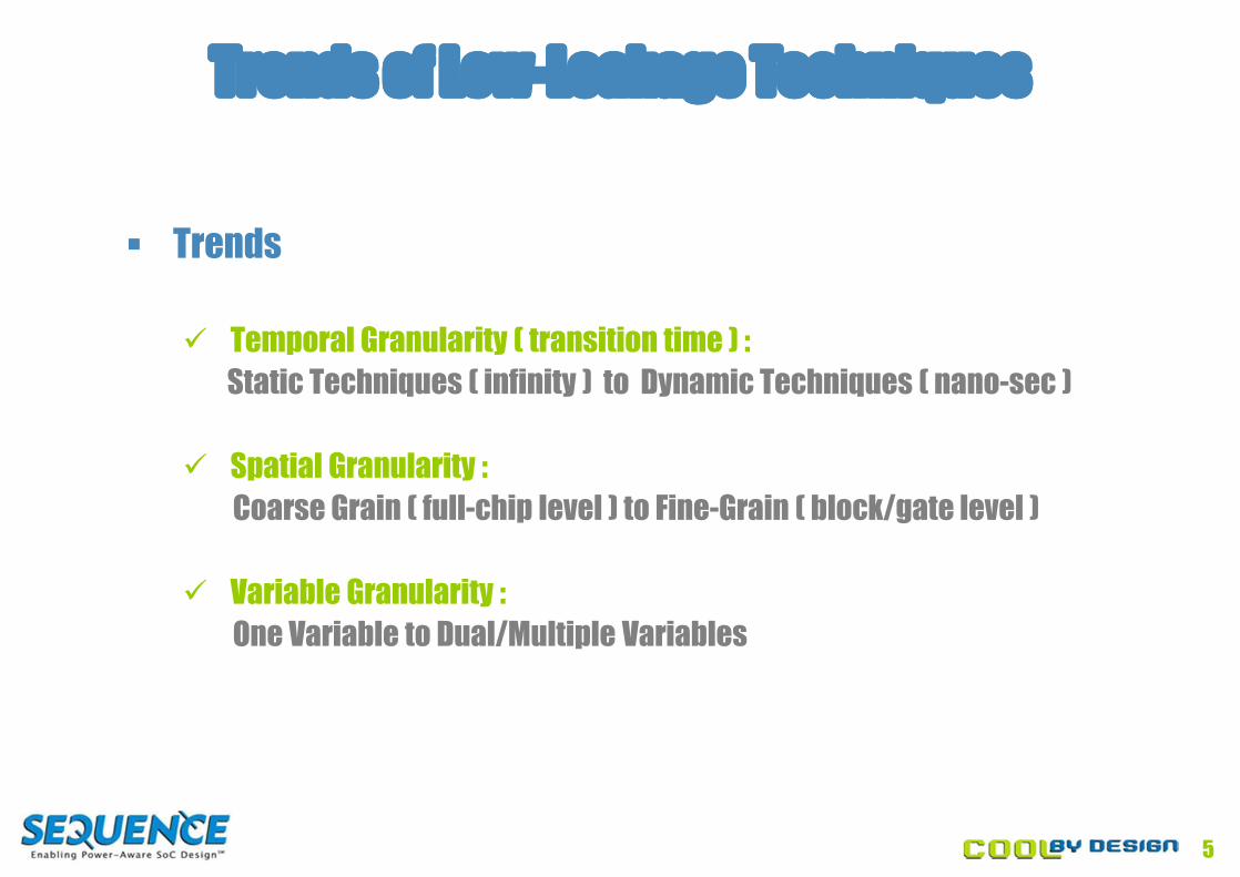
Trends of Low-Leakage TechniquesTrends of Low-Leakage Techniques
§ Trends
ü Temporal Granularity ( transition time ) :Static Techniques ( infinity ) to Dynamic Techniques ( nano-sec )
ü Spatial Granularity :Coarse Grain ( full-chip level ) to Fine-Grain ( block/gate level )
ü Variable Granularity :One Variable to Dual/Multiple Variables

6
Low-Leakage Techniques OverviewLow-Leakage Techniques Overview

7
1. Transistor Sizing1. Transistor Sizing
§ Shorter width means lower leakage, more delay, and lower dynamic power§ Issues
ü Given delay constraints, finding the optimal size for minimum power§ Pros
ü leakage reduction in both active and sleep modeü Fine-grained optimization is possibleü Simultaneously optimize width with Vdd and Vth
§ Consü Design automation complexity is highü Limited amount of leakage reduction
VDD
GNDC
GND
VDD
C

8
2. Transistor Stacking2. Transistor Stacking
§ Main factorsü Negative Vgs, Lowered signal rail (Vdd-Vs), Lower DIBL (lower Vdd-Vs), and Larger Body
Effect (negative Vbs)§ Issues
ü Given logic topology, maximizing stacking§ Pros
ü Design complexity is lowü No impact to technology scalingü Area and dynamic power overhead is generally low
§ Consü New cell library is needed
Ileakage µ 10(VGS-VTH)/S
DIBL
VTH = VTH0 – gVBS – lVDS
Body effect

9
3. Input Vector Control (IVC)3. Input Vector Control (IVC)
§ Different Input vector generates different leakage current, So there must be optimal primary input vectors which lead to the minimum leakage power in the standby mode
§ Issuesü Given logic topology, Finding the optimal input vector for minimum power
§ Prosü Easy to implementü Overhead is low in terms of delay, area, and dynamic powerü No impact to technology scaling
§ Consü Relatively less effective on leakage reduction
[ DAC 03, Lee ]
P-NET
N-NET
Sleep
HI P-NET
N-NET
Sleep
LO
[ VLSI Sym. 05, K. Choi ]

10
4. Dual/Multi-Vth Cell Swapping4. Dual/Multi-Vth Cell Swapping
§ Low-Vth cells on critical paths, High-Vth cells on non-critical paths§ Issues
ü Given delay constraints, finding the optimal Vths for minimum power without compromising the delay
§ Prosü No area overhead ü leakage reduction in both active and sleep mode
§ Consü Critical paths are still leakyü Limited amount of leakage reductionü Weak to technology scaling
F/F
F/F
F/F
F/F
F/F
F/F
F/F
F/F
F/F
F/F
F/F
F/F
F/F
Critical Path
HighVth
LowVth

11
5. Body Biasing ( VTCMOS )5. Body Biasing ( VTCMOS )
§ Reverse Body Biasing (RBB)ü Active Mode : No Bias ( = Low Vth ] and Sleep Mode : RBB ( = High Vth )
§ Forward Body Biasing (FBB)ü Active Mode : FBB ( = Low Vth ) and Sleep Mode : No Bias ( = High Vth)
§ Issuesü Given delay constraints, finding the optimal biasing for minimum power
§ Prosü Recently getting more attention as a post-silicon tuning for yield improvementü Dynamic approach is suitable
§ Consü Less effective at shorter channel length and lower Vthü Process complexity is high ( Triple well is needed )
[ ISLPED 01, A. Keshavarzi ]

12
6. Dynamic Voltage Scaling (DVS)6. Dynamic Voltage Scaling (DVS)
§ Dynamically scale energy/operation with throughput and exploit data dependent computation times to vary the supply voltage
§ Issuesü Given delay constraints, finding the optimal Vdd and Freq. for minimum power
§ Prosü Very effective to reduce total energy ( dynamic and leakage power )
§ Consü Difficult to implementü Additional Control circuits are needed for monitoring and scaling
Processor coreProcessor core
Voltagefrequencycontroller
Voltagefrequencycontroller
Clock & VDDClock & VDDControl info

13
7. MTCMOS Power Gating7. MTCMOS Power Gating
§ High Vth transistors gate leakage power during sleep mode for low Vth circuits§ Issues
ü Given delay constraints, finding the optimal clustering and the proper switch for minimum power
§ Prosü Most powerful leakage control scheme up to date ( 10x-100x reduction )ü Dynamic Fine-Grained approach is applicable
§ Consü Implementation complexity is high

14
Leakage Reduction Comparison (90nm)Leakage Reduction Comparison (90nm)1. Transistor Sizing 2. Transistor Stacking / 3. IVC 4. Dual/Multi-Vth Cell Swapping
5. Body Biasing (VTCMOS ) 6. DVS (Dynamic Voltage Scaling) 7. MTCMOS Power Gating
2x – 10x
5x – 10x
10x – 100x
2x – 5x 3x – 10x
3x – 5x

15
MTCMOS Power Gating IssuesMTCMOS Power Gating Issues
§ High Vth power switch sizing
§ Data retention
§ Floating Prevention
§ Ground bounce and rush current
§ P & R / Library
§ Wake-up time
§ Enable signaling

16
MTCMOS Power Gating Issues (1)MTCMOS Power Gating Issues (1)§ Power Switch Sizing
ü Basically trade-off between delay / area overhead and leakageü In dynamic approach, wake-up time and rush current are closely relatedü Gate/cell Based and Shared-Switch basedü ACM (Average Current Method), Mutually exclusive approach, and STA (Static
Timing Analysis) based approach
0 2 4 6 8 10 12 Power Switch Tr. Width (Wps/W)
Leak
age (
nano
ampe
re)
Delay
or A
rea
(Nor
mali
zed)
DelayNANDArea
Delay
Leakage1
1
AreaNAND
0.1
ODLeakNAND
[ VLSI Sym. 05, K. Choi ]
W = (R’ / V ) X I

17
MTCMOS Power Gating Issues (2)MTCMOS Power Gating Issues (2)§ Data retention and Floating Prevention during sleep mode
ü Special Flip-flop with data retentionü Preventing short-circuit current in un-gated blocks
[ Floating Prevention ]
[ Floating Prevention Circuit, Mutoh]

18
MTCMOS Power Gating Issues (3)MTCMOS Power Gating Issues (3)§ Dynamic control in a fine granularity
ü Active mode: ground bounceü Sleep mode: rush current and wake-up time ( < one cycle ) ü Solutions for rush current: Step-wise Turn-on and Transistor Chain
[ Active Mode ] [ Sleep Mode ]
[ Step-wise Turn-on ] [ Two Pass Power Switching Control ]
T1
T1
T2 Tn
T2 Tn
VssTurn On
Virtual Vss Virtual Vss
Vss
Turn-on REQ
Turn-on ACK
WeakPre-charge
Strong

19
MTCMOS Power Gating Issues (4)MTCMOS Power Gating Issues (4)§ P&R Issues
ü Mesh based power delivery is easily incorporated into standard design flow ( including Tapless library support)
ü Built-in buffer distributes driver circuitry, creating a buffer tree during power-gating control signal routing
[ Mesh Based ]
[ Tapless Design Example]§ Other Issues
ü How to control the power switches ( activation/deactivation ) ?ü When to off ? (Trade-off between switching power and leakage reduction )

20
One Last Thing . . .One Last Thing . . .§ In the future technologies, PVT (Process, Voltage, and Temperature)
Variations should be very carefully considered with the leakage reduction techniques !!

21
Summary and ConclusionsSummary and Conclusions
§ Leakage is a tough problem
§ Leakage becomes worse with each new process
§ Process engineers will not solve the leakage problema Designers must solve it
§ Multiple design solutions
§ MTCMOS power gating will become dominant

22/36