Genetic Drift Genetic Drift Genetic Bottleneck The Founder Effect.
ECE 695Numerical Simulations
Lecture 15: Advanced Drift-Diffusion Simulations
Prof. Peter Bermel
February 13, 2017

Outline
• Drift Diffusion Model Physical Effects
• Sentaurus
• Applications:
– Transistor Modeling
– Introduction of Trap States
– Effects of Radiation Strikes
2/13/2017 ECE 695, Prof. Bermel 2

Drift-Diffusion Model: Physical Effects
Physics Models
Mobility Concentration-dependent mobility (fit to experimental data), Parallel
field dependent mobility (fit to experimental saturation velocities)
Generation recombination and trapping
Modified concentration dependentShockley-Read-Hall
Generation/recombination (for treatment of defects)
Impact ionization Selberherr’s impact ionization model
Tunneling Band-to-band tunneling, Trap-Assistedtunneling
Oxide physics Fowler-Nordheim tunnelling, interface charge accumulation
ECE 695, Prof. Bermel 32/13/2017

Sentaurus Workbench• Run command: swb• Graphical user interface to unify all simulation tools
into a single experiment project flow• Used to organize projects and set up experiments
for both structure generation and device simulation
Technology Computer-Aided-Design Tools
Parameter row
Experiment column2/13/2017 ECE 695, Prof. Bermel 4
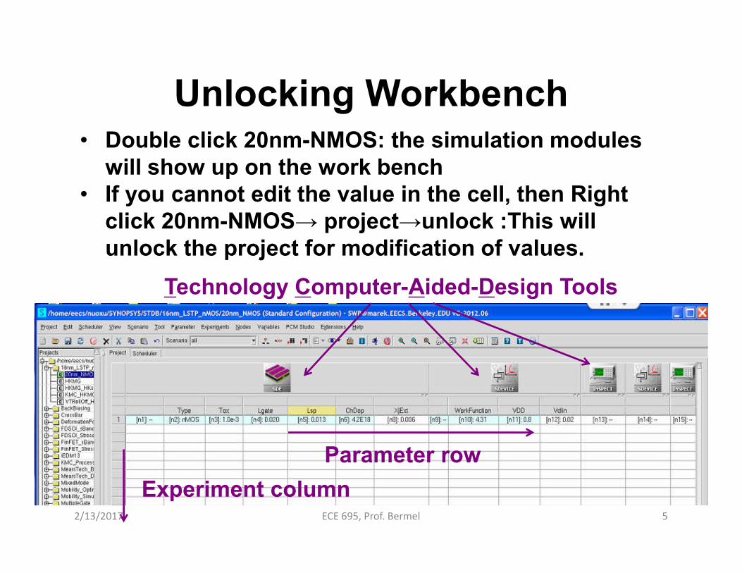
Unlocking Workbench• Double click 20nm-NMOS: the simulation modules
will show up on the work bench• If you cannot edit the value in the cell, then Right
click 20nm-NMOS→ project→unlock :This will unlock the project for modification of values.
Technology Computer-Aided-Design Tools
Parameter row
Experiment column2/13/2017 ECE 695, Prof. Bermel 5

Sentaurus Structure Editor• Recommended to run in workbench
• Run command (under putty): sde
• Structure Editor (1) generates the device structure (including the doping profiles) (2) Defines the electrical contact and (3) generates the meshing for numerical simulations.
Parameters you may need to change/optimize for this project• Gate oxide thickness (Xo, Units: um)• MOSFET gate length (Lgate, Units: um)• Spacer length (Lsp, Units: um)• Channel Doping Concentration (ChanDoping, Units: cm-3)• Source/Drain extension depth (XjExt, Units: um)
2/13/2017 ECE 695, Prof. Bermel 6

Sentaurus Device• Recommended to run in workbench
• Run command (under putty): sdevice
• Sentaurus Device simulates the device performance by solving multiple, coupled physical equations based on the meshing.
• Inputs: gate voltage (Vgs), drain voltage (Vds), workfunction value
Common Physical models:• Si band structure (Ec/v, Nc/v and bandgap narrowing)• Fermi-Dirac Statistics• Poisson equation, continuity equation• Band-to-band tunneling, R-G current• Drift-Diffusion current, carrier mobility, velocity saturation
2/13/2017 ECE 695, Prof. Bermel 7

Sentaurus Inspect• Recommended to run in workbench• Used to automatically extract critical
device performance parameters such as:Vt_lin Id_linVt_sat Id_sat I_OFF
• Also used to plot the Id-Vg and Id-Vd
curves
2/13/2017 ECE 695, Prof. Bermel 8

Simulation Status• Start Sentaurus, first select from the left project
column, right-click to “preprocess”.
• Then you will find the nodes will display different colors, suggesting they have different properties. Here is a summary. Only colorful nodes will give you the simulation output.
• “Ready” means the current tool is free of syntax errors (You should see this since you are not allowed to modify the scripts).
• Right-click a certain Ready nodes to run, after a short period of time, you will find it changes to “done” or “failed”.
2/13/2017 ECE 695, Prof. Bermel 9
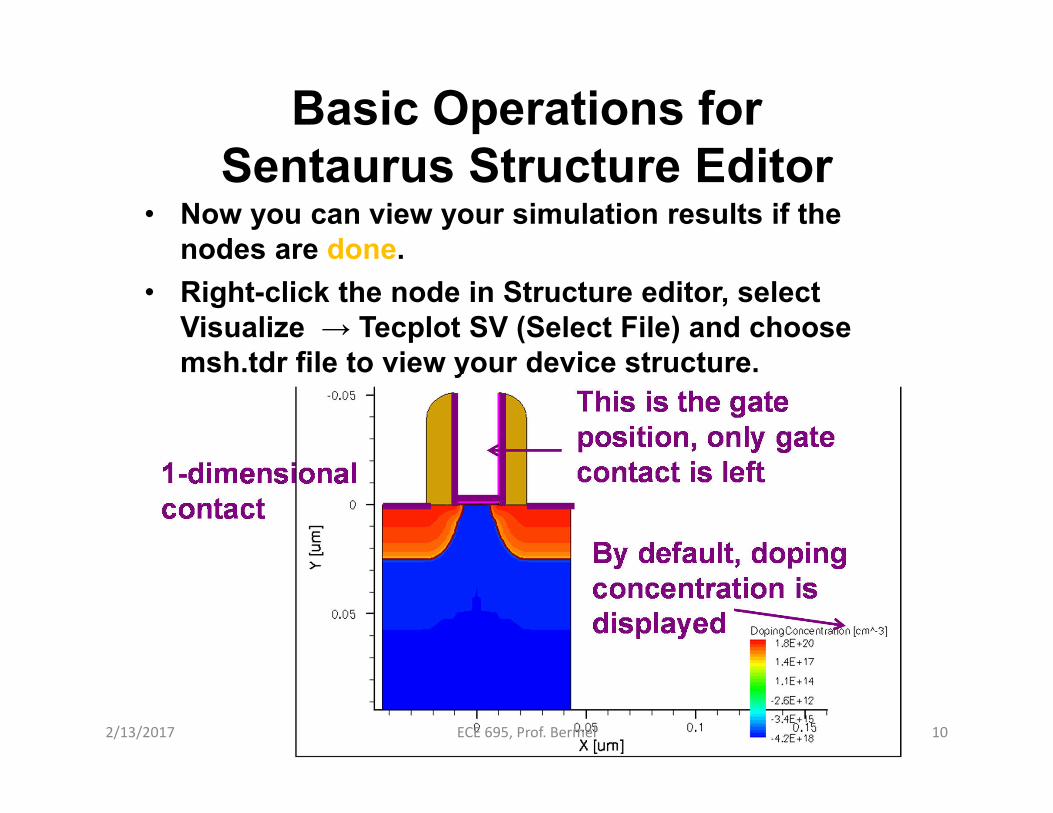
Basic Operations for Sentaurus Structure Editor
• Now you can view your simulation results if the nodes are done.
• Right-click the node in Structure editor, select Visualize → Tecplot SV (Select File) and choose msh.tdr file to view your device structure.
2/13/2017 ECE 695, Prof. Bermel 10
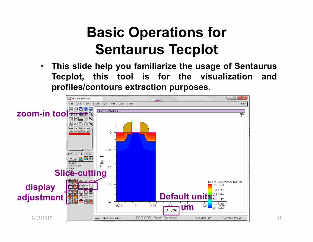
Basic Operations for Sentaurus Tecplot
• This slide help you familiarize the usage of SentaurusTecplot, this tool is for the visualization andprofiles/contours extraction purposes.
zoom-in tool
display adjustment
Slice-cutting
Default units: um
2/13/2017 ECE 695, Prof. Bermel 11

Export the results from Tecplot:
As an image (.bmp)
To get the data field,first, use Y-cut to get the1-D slice; then selectexport → Inspect graph
2/13/2017 ECE 695, Prof. Bermel 12

Then Inspect will be started.
Select the data field herein; Click File → Export → txt file
You can read your saved data (.txt file)from your project directory2/13/2017 ECE 695, Prof. Bermel 13

Basic Operations for Sentaurus Device
• Right-click the “done” node in Structure Device, select Visualize → Tecplot SV (Select File) and choose des.tdr file to view your device performance contours (vector fields).
Linear region Saturation region
Current Density
2/13/2017 ECE 695, Prof. Bermel 14

Basic Operations for Sentaurus Device Cont.’d
• Right-click the “done” node in Structure Device, select Visualize → Inspect (Select File) and choose IdVg_des.plt file to view your device performance curves.
Choose Log Y or Linear Y here
Use cursors to read the data value along the curve
Most common plot combination is “gate: OuterVoltage”
“drain: TotalCurrent”
Device Terminals
Outputs
2/13/2017 ECE 695, Prof. Bermel 15

Idsat, Ilin and IOFF
VDD
IOFF
Idsat
Ilin
Vds=VDD
Vds=20mV
IOFF, Idsat and Idlin
are extractedautomatically
2/13/2017 ECE 695, Prof. Bermel 16
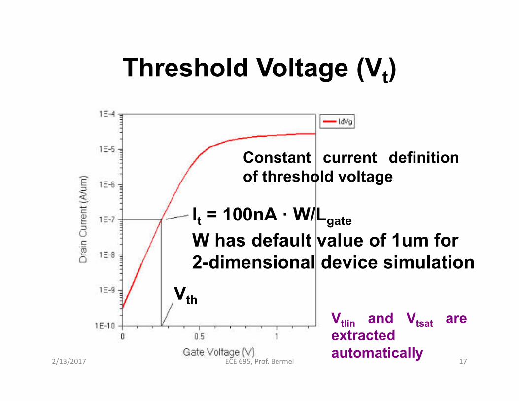
Threshold Voltage (Vt)
Constant current definitionof threshold voltage
Vth
It = 100nA · W/Lgate
W has default value of 1um for 2-dimensional device simulation
Vtlin and Vtsat areextractedautomatically
2/13/2017 ECE 695, Prof. Bermel 17

DIBL and SS
Sub-threshold SwingDIBL is defined as the thresholdvoltage difference divided by thedrain bias between linear andsaturation region .
2/13/2017 ECE 695, Prof. Bermel 18
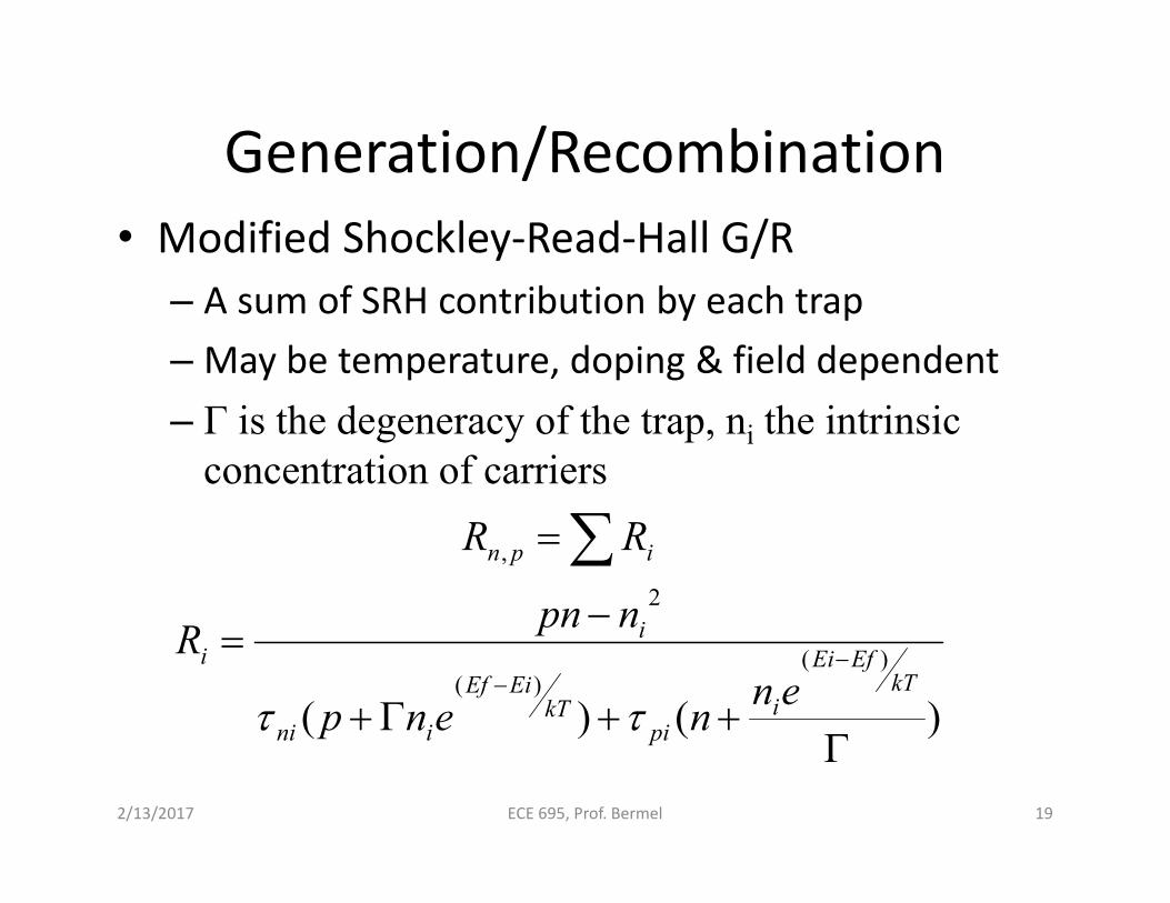
Generation/Recombination• Modified Shockley-Read-Hall G/R
– A sum of SRH contribution by each trap
– May be temperature, doping & field dependent
– Γ is the degeneracy of the trap, ni the intrinsic concentration of carriers
ECE 695, Prof. Bermel 19
)()(
)()(
2
,
kTEfEi
ipi
kTEiEf
ini
ii
ipn
ennenp
npnR
RR
tt
2/13/2017

Generation/Recombination• Transient behaviour of traps
σn,p is trap capture cross-sectionvn,p is thermal velocityni is intrinsic concentrationFtA,TD the probability of ionizationNtA,TD space charge density ECE 695, Prof. Bermel 20
))1(
())1((
))1(
())1((
kTEE
itAtApp
kTEE
itAtAnnttA
kTEE
itDtDnn
kTEE
itDtDppttD
tiit
itti
enF
pFvenFFnvdt
dN
enF
nFvenFFpvdt
dN
pptrap
p
nntrap
nt
t
11
Electron capture
Electronemission
Holecapture
Holeemission
holecapture
holeemission
electroncapture
electronemission
2/13/2017
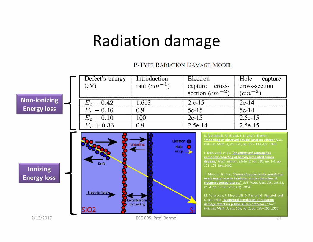
Radiation damage
ECE 695, Prof. Bermel 21
Non-ionizingEnergy loss
IonizingEnergy loss
D. Menichelli, M. Bruzzi, Z. Li, and V. Eremin, “Modelling of observed double-junction effect,” Nucl. Instrum. Meth. A, vol. 426, pp. 135–139, Apr. 1999.
F. Moscatelli et al., “An enhanced approach to numerical modeling of heavily irradiated silicon devices,” Nucl. Instrum. Meth. B, vol. 186, no. 1-4, pp. 171–175, Jan. 2002.
F. Moscatelli et al., “Comprehensive device simulation modeling of heavily irradiated silicon detectors at cryogenic temperatures,” IEEE Trans. Nucl. Sci., vol. 51, no. 4, pp. 1759–1765, Aug. 2004.
M. Petasecca, F. Moscatelli, D. Passeri, G. Pignatel, and C. Scarpello, “Numerical simulation of radiation damage effects in p-type silicon detectors,” Nucl. Instrum. Meth. A, vol. 563, no. 1, pp. 192–195, 2006.
2/13/2017

Impact ionization
22ECE 695, Prof. Bermel
e
ep
EpB
nE
nB
pp
nn
ppnn
A
A
JEJEG
b
b
a
a
aa
)(
)(
)()(
Selberherr, S., "Analysis and Simulation of Semiconductor Devices", Springer-Verlag Wien New York, ISBN 3-211-81800-6, 1984.
2/13/2017

Phonon-assisted trap-to-band tunneling
ECE 695, Prof. Bermel 23
)(1
)(1
)(
0)(
0
2
kT
EfEi
iDIRACp
pkTEiEf
iDIRACn
n
ii
ennenp
npnR
tt
duekT
E
duekT
E
uKukT
E
L
pDIRACp
uKukT
E
L
nDIRACn
pL
p
nL
n
1
0
)(
1
0
)(
23
23
Eq
EmmK
Eq
EmmK
ptunnel
p
ntunneln
3
2
3
4
3
2
3
4
3
0
3
0
Hurkx, G.A.M., D.B.M. Klaasen, M.P.G. Knuvers, and F.G. O’Hara,“A New Recombination Model Describing Heavy-Doping Effects
and Low Temperature Behaviour”, IEDM Technical Digest(1989): 307-310.
2/13/2017

24
n+
S
n+
p-substrate
G
D
VDD
Depletion Region
Radiation Particle
_ ++_
_+
_+_
+ _+_+
E_+
VDD - VjnE
Charge Deposition by a Radiation Particle
• Radiation particles - protons, neutrons, alpha particles and heavy ions
• Reverse biased p-n junctions are most sensitive to particle strikes
Charge is collected at the drain node through drift and diffusion
Results in a voltage glitch at the drain node
System state may change if this voltage glitch is captured by at least one memory element
This is called an SEU
May cause system failureB2/13/2017 ECE 695, Prof. Bermel
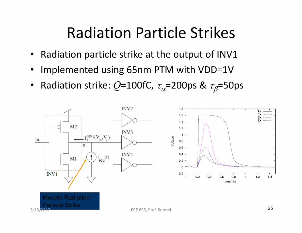
25
Radiation Particle Strikes• Radiation particle strike at the output of INV1
• Implemented using 65nm PTM with VDD=1V
• Radiation strike: Q=100fC, ta=200ps & tb=50ps
Models Radiation Particle Strike
2/13/2017 ECE 695, Prof. Bermel

NMOS Device Modeling • Constructed NMOS transistors using
Sentaurus-Structure editor tool
• Gate length 35nm, Tox = 1.2nm spacer width = 30nm
• A heavy ion strikes at the center of the drain
26
in out1
INV
Cload
3D Device Model
SPICE Model
D S
G
Halo implants VT implant
Punch through implant
Well Contact
Heavy Ion
2/13/2017 ECE 695, Prof. Bermel

NMOS Device Characterization
• Characterized the NMOS device using Sentaurus-DEVICE
• Width = 1mm
• Good MOSFET characteristics
272/13/2017 ECE 695, Prof. Bermel

Results and Discussions
• O1 – Small devices collect less charge compared to large devices– Reverse biased electric field is present for shorter duration in small devices
– Lower drain area – less charge is collected through diffusion
• G1 – If we upsize a gate to harden it, a higher value of Qcoll should be used– Extremely important for low voltage operation
– O1.1 – For low energy strikes, Qcoll remains roughly constant across different gate sizes for nominal voltage operation
282/13/2017 ECE 695, Prof. Bermel

Next Class
Will cover band structure theory and modeling techniques