ECE 371 Microprocessor Interfacing
32
ECE 371 Microprocessor Interfacing Unit 2 - Introduction to the MC9S12DP256B Microcontroller
-
Upload
aladdin-blackburn -
Category
Documents
-
view
90 -
download
2
description
ECE 371 Microprocessor Interfacing. Unit 2 - Introduction to the MC9S12DP256B Microcontroller. 16-bit Microcontroller Family (Partial List). •MC9S12D64 MC9S12DG128B MC9S12DP256B (our chip) MC9S12DP512. Product Numbering System. MC 9 S12 DP 256 B Status. Memory type. - 9:flash. - PowerPoint PPT Presentation
Transcript of ECE 371 Microprocessor Interfacing
ECE 371Microprocessor Interfacing
Unit 2 - Introduction to the MC9S12DP256B Microcontroller
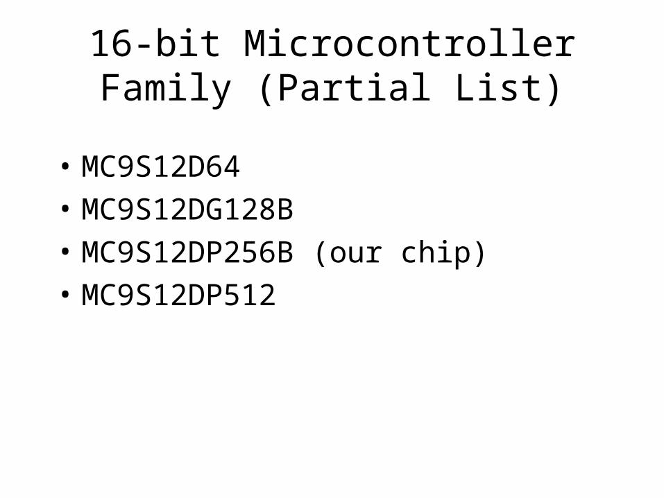
16-bit Microcontroller Family (Partial List)
• MC9S12D64
• MC9S12DG128B
• MC9S12DP256B (our chip)
• MC9S12DP512

Product Numbering System
MC 9 S12 DP 256 B Status
Memory type
- 9:flash
Core type
Family
Approximate memory size
Flash revision
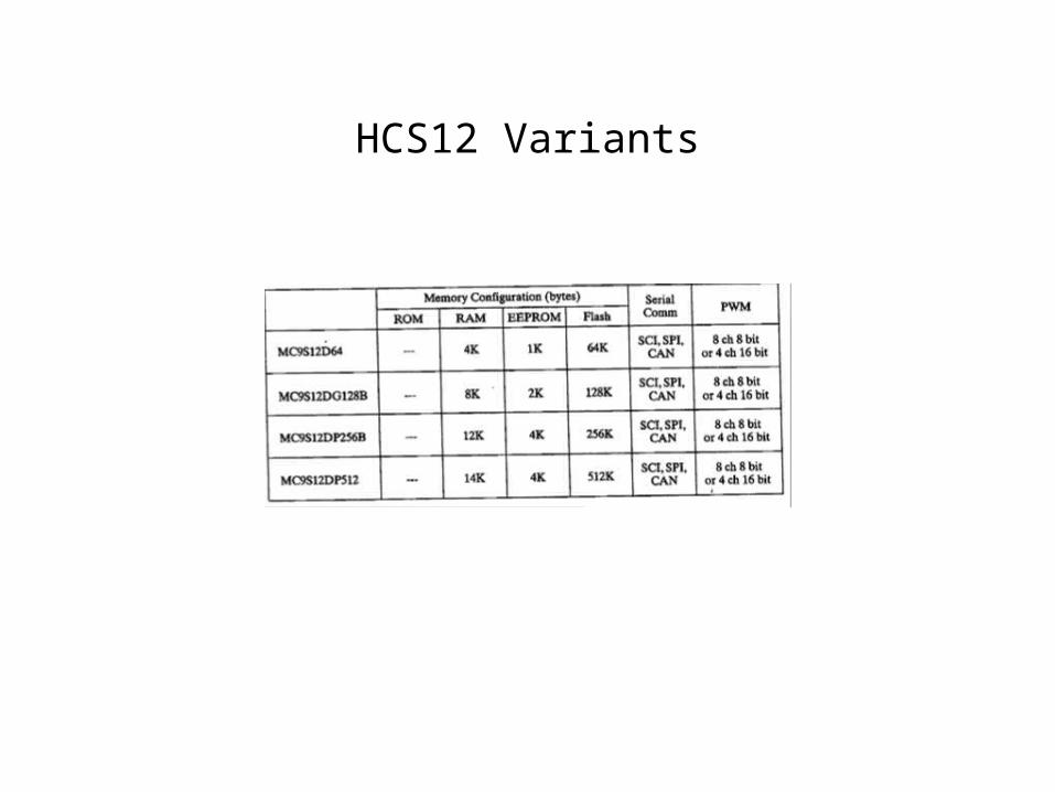
HCS12 Variants


68HC12 References
• http://www.freescale.com– products -> microcontrollers -> 16 bit
microcontrollers– documentation -> microcontrollers -> 16 bit
microcontrollers
• Lab Computers – Files
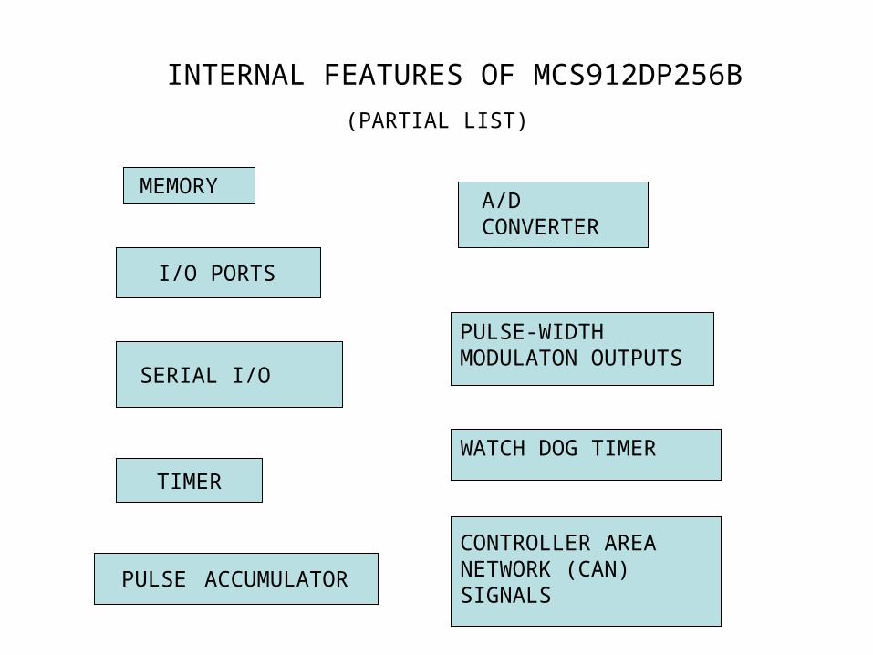
MEMORY
TIMER
PULSE ACCUMULATOR
I/O PORTS
SERIAL I/O
A/D CONVERTER
PULSE-WIDTH MODULATON OUTPUTS
WATCH DOG TIMER
CONTROLLER AREA NETWORK (CAN) SIGNALS
INTERNAL FEATURES OF MCS912DP256B
(PARTIAL LIST)

INTERNAL MEMORY OF MCS912DP256B
• 12 K BYTES OF RAM(PROGRAM CODE, VARIABLES, AND STACK)
• 4K BYTES OF EEPROM(SYSTEM DATA)
• 256K BYTES OF FLASH EEPROM (PROGRAM CODE)
• ALSO 2K BYTES FOR REGISTERS
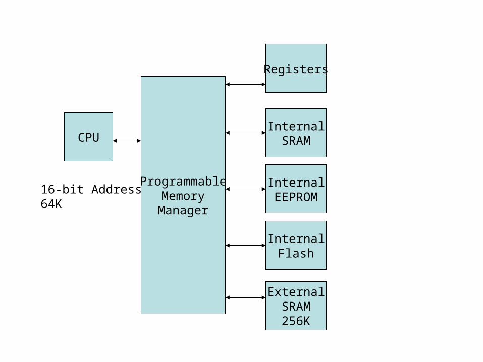
CPU
ProgrammableMemoryManager
Registers
InternalSRAM
InternalEEPROM
InternalFlash
ExternalSRAM256K
16-bit Address64K

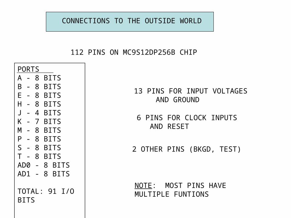
112 PINS ON MC9S12DP256B CHIP
PORTSA - 8 BITSB - 8 BITSE - 8 BITSH - 8 BITSJ - 4 BITSK - 7 BITSM - 8 BITSP - 8 BITSS - 8 BITST - 8 BITSAD0 - 8 BITSAD1 - 8 BITS
TOTAL: 91 I/O BITS
13 PINS FOR INPUT VOLTAGES AND GROUND
6 PINS FOR CLOCK INPUTS AND RESET
2 OTHER PINS (BKGD, TEST)
CONNECTIONS TO THE OUTSIDE WORLD
NOTE: MOST PINS HAVEMULTIPLE FUNTIONS
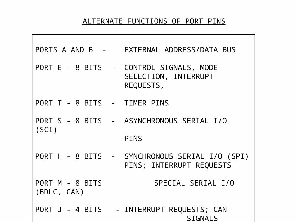
ALTERNATE FUNCTIONS OF PORT PINS
PORTS A AND B - EXTERNAL ADDRESS/DATA BUS
PORT E - 8 BITS - CONTROL SIGNALS, MODE SELECTION, INTERRUPT REQUESTS,
PORT T - 8 BITS - TIMER PINS
PORT S - 8 BITS - ASYNCHRONOUS SERIAL I/O (SCI) PINS
PORT H - 8 BITS - SYNCHRONOUS SERIAL I/O (SPI) PINS; INTERRUPT REQUESTS
PORT M - 8 BITS SPECIAL SERIAL I/O (BDLC, CAN)
PORT J - 4 BITS - INTERRUPT REQUESTS; CAN SIGNALS

PORT P - 8 BITS - PULSE WIDTH MODULATION (PWM)OUTPUTS; INTERRUPT REQUESTS
PORT K - 7 BITS - ADDRESS LINES A19-A14 FOR EXPANDED (EXTERNAL ACCESS
MODE)
PORT AD0 - 8 BITS - INPUTS TO A/D CONVERTER 0
PORT AD1 - 8 BITS - INPUTS TO A/D CONVERTER 1
MORE ALTERNATE FUNCTIONS OF PORT PINS
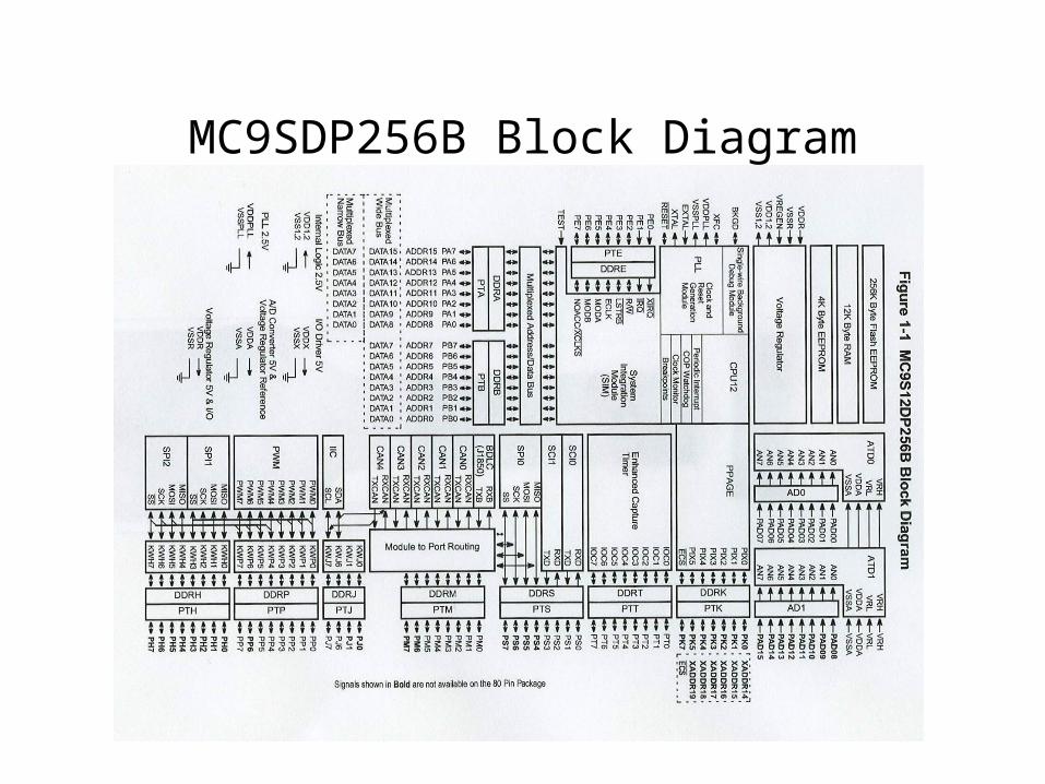
MC9SDP256B Block Diagram
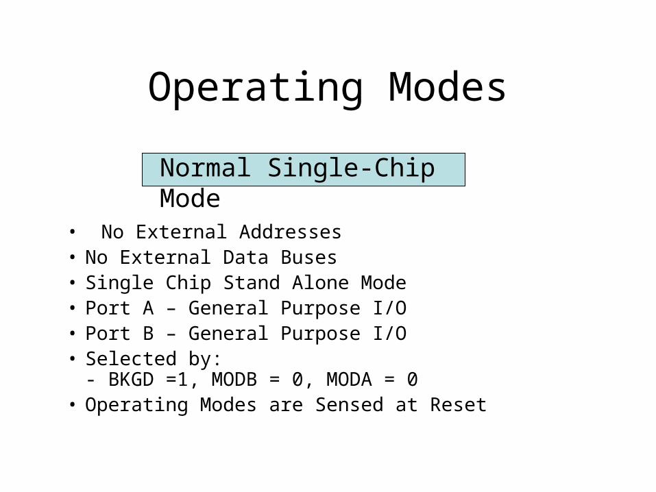
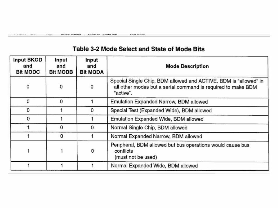
Operating Modes
• No External Addresses• No External Data Buses• Single Chip Stand Alone Mode• Port A – General Purpose I/O• Port B – General Purpose I/O• Selected by:
- BKGD =1, MODB = 0, MODA = 0• Operating Modes are Sensed at Reset
Normal Single-Chip Mode
Operating Modes
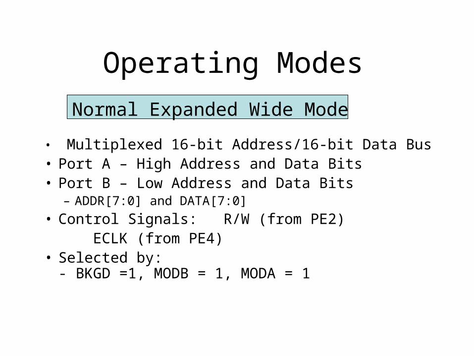
• Multiplexed 16-bit Address/16-bit Data Bus• Port A – High Address and Data Bits• Port B – Low Address and Data Bits
– ADDR[7:0] and DATA[7:0]
• Control Signals: R/W (from PE2) ECLK (from PE4)
• Selected by:- BKGD =1, MODB = 1, MODA = 1
Normal Expanded Wide Mode
Operating Modes
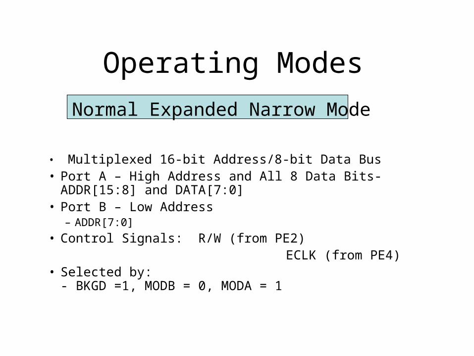
• Multiplexed 16-bit Address/8-bit Data Bus• Port A – High Address and All 8 Data Bits- ADDR[15:8] and
DATA[7:0]• Port B – Low Address
– ADDR[7:0]
• Control Signals: R/W (from PE2) ECLK (from PE4)• Selected by:
- BKGD =1, MODB = 0, MODA = 1
Normal Expanded Narrow Mode


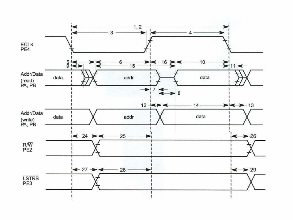
ADDR7 - ADDR0/ DATA7 - DATA0
ADDR 15 - ADDR8/ DATA15 - DATA8
PB7 - PB0
PA7 - PA0
MULTIPLEXED WIDE BUS
R/W
ECLK
PE2
PE4(EXTERNAL BUSCLOCK)
LSTRBPE3
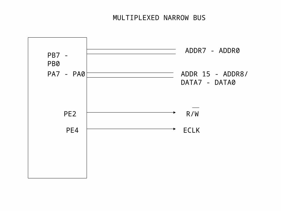
ADDR7 - ADDR0
ADDR 15 - ADDR8/ DATA7 - DATA0
PB7 - PB0
PA7 - PA0
MULTIPLEXED NARROW BUS
R/W
ECLK
PE2
PE4

Access Type vs. Bus Control Pins
Table 12-5 Access Type vs. Bus Control Pins
/LSTRB A0 R/W Type of Access 1 0 1 8-bit read of an even address 0 1 1 8-bit read of an odd address 1 0 0 8-bit write of an even address 0 1 0 8-bit write of an odd address 0 0 1 16-bit read of an even address 1 1 1 XXX 0 0 0 16-bit write to an even address 1 1 0 XXX

Interface to 16-bit Data Bus
128K x 8 128K x 8
D15 .. D8High Byte
D7 .. D0Low Byte
A17 .. A1 A17 .. A1
/cs1cs2/oe/we
/cs1cs2/oe/we

ADDR7 - ADDR0
ADDR 15 - ADDR8
PB7 - PB0
PA7 - PA0
ADDRESS LATCHES
ECLKPE4
CLK
CLK
ADDRESS LATCHED BY ON CLK
MC9SDP256B12

ADR2 ADR3 ADR4ADR1
DAT1 DAT2 DAT3 DAT3
ADR1 ADR2 ADR3 ADR4
ECLK
DemultiplexedAddress
Demultiplexed Address

PK5 - PK0 XADDR19 - XADDR 14
PK7 ECS
(IF ECS = 0, USE XADDR19 - XADDR 14,ALONG WITH ADDR13 - ADDR0)
(IF ECS = 1, USE ONLYADDR15 - ADDR0)
MC9SDP256B12
PAGE ADDRESSING FOR EMULATION EXPANDED MODES
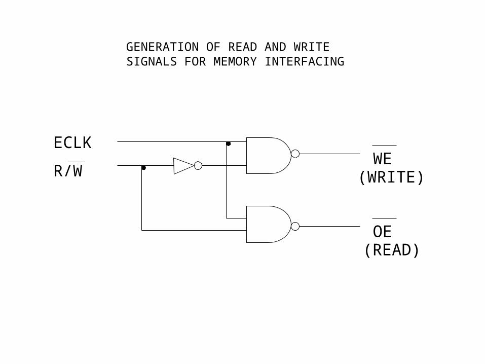
WE
OE
ECLK
R/W
(READ)
(WRITE)
GENERATION OF READ AND WRITE SIGNALS FOR MEMORY INTERFACING


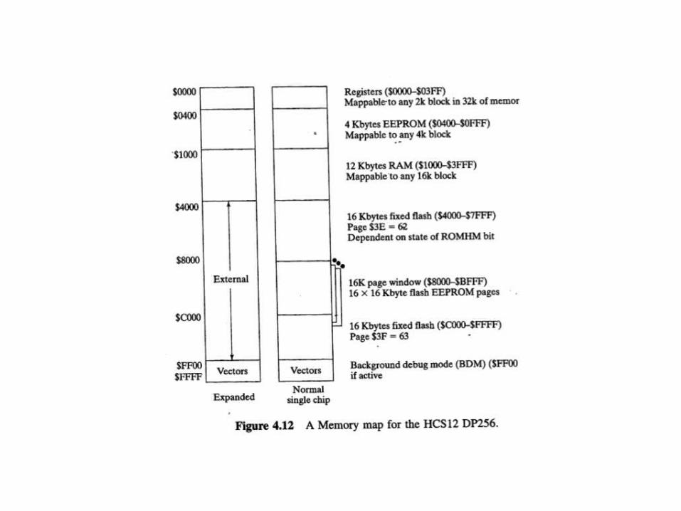
In the Normal Expanded Narrow Mode and the Normal Expanded Wide Mode, the Page Window Access Memory Region Can be Allocated Between External Memory and Internal Memory
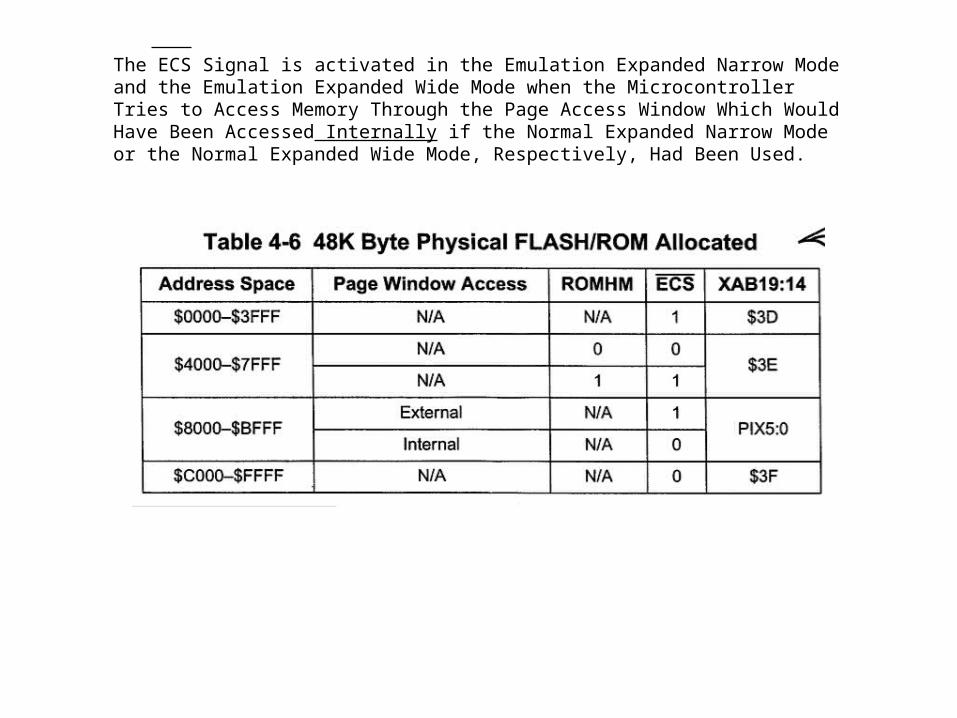
The ECS Signal is activated in the Emulation Expanded Narrow Mode and the Emulation Expanded Wide Mode when the Microcontroller Tries to Access Memory Through the Page Access Window Which Would Have Been Accessed Internally if the Normal Expanded Narrow Mode or the Normal Expanded Wide Mode, Respectively, Had Been Used.