Dual Band, Dual Polarization Array Antenna for mm-Wave...
74
Dual Band, Dual Polarization Array Antenna for mm-Wave Radio Capped Bow-Tie Antenna Elements in a Tightly Coupled Array Antenna Master’s thesis in Wireless, Photonics and Space Engineering NIKOLAOS FOKOS ERICSSON AB & Department of Signals and Systems CHALMERS UNIVERSITY OF TECHNOLOGY Gothenburg, Sweden 2017
-
Upload
duongtuong -
Category
Documents
-
view
228 -
download
0
Transcript of Dual Band, Dual Polarization Array Antenna for mm-Wave...
Dual Band, Dual Polarization ArrayAntenna for mm-Wave RadioCapped Bow-Tie Antenna Elements in a Tightly Coupled ArrayAntenna
Master’s thesis in Wireless, Photonics and Space Engineering
NIKOLAOS FOKOS
ERICSSON AB & Department of Signals and SystemsCHALMERS UNIVERSITY OF TECHNOLOGYGothenburg, Sweden 2017


Master’s thesis 2017:NN
Dual Band, Dual Polarization Array Antenna formm-Wave Radio
Capped Bow-Tie Antenna Elements in a Tightly Coupled ArrayAntenna
NIKOLAOS FOKOS
Department of Signals and SystemsDivision of Antenna Systems
Chalmers University of TechnologyGothenburg, Sweden 2017

Dual Band, Dual Polarization Array Antenna for mm-Wave RadioCapped Bow-Tie Antenna Elements in a Tightly Coupled Array AntennaNIKOLAOS FOKOS
© NIKOLAOS FOKOS, 2017.
Supervisors: Stefan Thöresson, Ericsson ABLars Manholm, Ericsson ABMartin N. Johansson, Ericsson AB
Examiner: Prof. Jian Yang, Department of Signals and Systems
Master’s Thesis 2017:NNDepartment of Signals and SystemsDivision of Antenna SystemsChalmers University of TechnologySE-412 96 GothenburgTelephone +46 31 772 1000
Ericsson ABSE-417 56 GothenburgTelephone +46 10 719 0000
Cover: Capped bow-tie array antenna visualization constructed in HFSS.
Typeset in LATEXGothenburg, Sweden 2017
iv

Dual Band, Dual Polarization Array Antenna Element for mm-Wave RadioCapped Bow-Tie Antenna Elements in a Tightly Coupled Array AntennaNIKOLAOS FOKOSEricsson ABDepartment of Signals and SystemsChalmers University of Technology
AbstractThe combination of a traditional point-to-point (PtP) frequency band and E-bandin a single radio unit will increase the spectrum efficiency, the peak capacity, theeffective throughput and the service availability for wireless backhaul. The dualpolarization capped bow-tie antenna element in a tightly coupled array (TCA) con-figuration is designed to perform as a dual band (23 GHz band and E-band), dualpolarization PtP planar array antenna. The planar array is implemented in printedcircuit board (PCB) technology, which is low cost, flexible and provide high mechan-ical reliability. TCAs have ultra-wideband performance when placed above a groundplane, as well as high scalability, so as they can be tuned for different combinationsof dual band operation inside a fractional bandwidth of 4.2:1. The return loss of thisdesign is more than 15 dB in both bands and the polarization orthogonality is morethan 27 dB in 23 GHz band, and more than 15 dB in E-band with potential to reach27 dB. The isolation between horizontal and vertical polarization ports for 23 GHzband is more than 20 dB and from 10 dB to 15 dB for E-band. The return loss ofthe design displays a shift in frequency in lower band and 2 dB to 6 dB degradationin the higher band with 10% variance of the structure’s dimensions, as the elementimpedance is affected. In addition, a 2-by-1 sub-array is proposed for fabricationand measurement in order to validate the design.
Keywords: Dual band, Dual polarization, E-band, PCB array antennas, TCAs,Wireless backhaul, PtP antennas
v


AcknowledgementsI would like to express my appreciation to my supervisor Stefan Thöresson and tomy manager Daniel Gillén from Ericsson AB for giving me the opportunity to workwith this project. A special gratitude I give to my co-supervisors Lars Manholmand Martin N. Johansson for their stimulating suggestions and their guidance to theright path.Furthermore I would also like to thank Sadegh Mansouri Moghaddam for his helpand support during this period. Finally, a special thank you to Prof. Jian Yang notonly for being my examiner but also for his continuous encouragement.
Nikolaos Fokos, Gothenburg, June 2017
vii


Abbreviationsbalun Balance to unbalance
GSG Ground-signal-ground
HOR Horizontal
LOS Line-of-sight
NLOS Non Line-of-sight
PCB Printed circuit board
PtP Point-to-point
PtMP Point-to-multi-point
TCA Tightly coupled array
UWB Ultra-wide band
VER Vertical
VSWR Voltage standing wave ratio
XPD Cross-polarization decoupling
ix


Contents
List of Figures xiii
List of Tables xvii
1 Introduction 11.1 Motivation . . . . . . . . . . . . . . . . . . . . . . . . . . . . . . . . . 11.2 Thesis Contribution . . . . . . . . . . . . . . . . . . . . . . . . . . . . 21.3 Thesis Outline . . . . . . . . . . . . . . . . . . . . . . . . . . . . . . . 2
2 Theory 52.1 Planar Phased Array Antennas . . . . . . . . . . . . . . . . . . . . . 5
2.1.1 Radiation Fields . . . . . . . . . . . . . . . . . . . . . . . . . 62.1.2 Grating Lobes . . . . . . . . . . . . . . . . . . . . . . . . . . . 72.1.3 Steering Main Lobe . . . . . . . . . . . . . . . . . . . . . . . . 92.1.4 Polarization . . . . . . . . . . . . . . . . . . . . . . . . . . . . 92.1.5 Directivity . . . . . . . . . . . . . . . . . . . . . . . . . . . . . 102.1.6 Array Gain . . . . . . . . . . . . . . . . . . . . . . . . . . . . 11
2.2 Tightly Coupled Array Antennas . . . . . . . . . . . . . . . . . . . . 132.3 Balance to Unbalance Feeding Structures . . . . . . . . . . . . . . . . 162.4 UWB Antenna Research Activities at Chalmers University of Tech-
nology . . . . . . . . . . . . . . . . . . . . . . . . . . . . . . . . . . . 18
3 Design Analysis and Simulated Results 193.1 Dual Polarization Capped Bow-Tie TCA . . . . . . . . . . . . . . . . 19
3.1.1 Dual Polarization Bow-Tie Element . . . . . . . . . . . . . . . 193.1.2 Analysis of Dual Polarization Capped Bow-Tie TCA . . . . . 203.1.3 Feeding Structure . . . . . . . . . . . . . . . . . . . . . . . . . 21
3.2 Simulated Results . . . . . . . . . . . . . . . . . . . . . . . . . . . . . 223.2.1 Return Loss and Isolation . . . . . . . . . . . . . . . . . . . . 24
3.2.1.1 Common-mode Resonance Frequencies Analysis . . . 253.2.2 Co-Polarization and Cross-Polarization . . . . . . . . . . . . . 273.2.3 Radiation Patterns . . . . . . . . . . . . . . . . . . . . . . . . 30
3.3 Beam Steering . . . . . . . . . . . . . . . . . . . . . . . . . . . . . . . 313.4 Tolerance Analysis . . . . . . . . . . . . . . . . . . . . . . . . . . . . 34
3.4.1 Dimension Tolerance Analysis . . . . . . . . . . . . . . . . . . 343.4.2 Material Tolerance Analysis . . . . . . . . . . . . . . . . . . . 40
xi

Contents
4 Measurement and Fabrication Considerations 434.1 Transition from Element to Probe Pad . . . . . . . . . . . . . . . . . 444.2 Prototype Simulated Results . . . . . . . . . . . . . . . . . . . . . . . 46
5 Conclusion 515.1 General Conclusions . . . . . . . . . . . . . . . . . . . . . . . . . . . 515.2 Future Work Proposal . . . . . . . . . . . . . . . . . . . . . . . . . . 52
Bibliography 53
xii

List of Figures
2.1 Rectangular grid with positions of the elements of the planar array. . 62.2 (a) Array factor with main and grating lobes, (b) Total radiation
pattern [33]. . . . . . . . . . . . . . . . . . . . . . . . . . . . . . . . . 82.3 Gain limitation with line losses at 86 GHz for eradegrtepoleill = 1. . . . 122.4 Gain limitation with line losses at 21 GHz for eradegrtepoleill = 1. . . . 122.5 Gain limitation with line losses at 86 GHz for eradegrtepoleill = 0.6. . . 132.6 Equivalent circuit for a tightly coupled array in free space [27]. . . . . 142.7 (Top) Equivalent circuit for an array in free space. (Bottom) Equiv-
alent circuit for an array with a ground plane [27]. . . . . . . . . . . . 152.8 Marchand balun diagram. . . . . . . . . . . . . . . . . . . . . . . . . 162.9 (a) Equivalent circuit of a differential feeding network [18]. (b) Lumped
impedance equivalent circuit [22] . . . . . . . . . . . . . . . . . . . . . 17
3.1 Progress of dual polarization capped bow-tie element. In the 2-by-1 sub-arrays that are shown the caps (hexagonal copper structures)have been removed from figure for better view of the element, as wellas the feeding parts. (a) First design, (b) Slotted element, (c) Slottedand shaped element, (d) Slotted element with extra design freedom. . 20
3.2 (a) Multi-layer PCB design of a 4-by-4 sub-array. (b) Substrate designparameters, feeding network included. . . . . . . . . . . . . . . . . . . 21
3.3 (a) Feeding network top view [18]. (b) Twin parallel wire. . . . . . . . 223.4 Design parameters of dual polarization capped bow-tie. (a) Element,
(b) Parasitic Cap, (c) Cap, (d) Feeding Stub. . . . . . . . . . . . . . . 233.5 Return loss simulation result for the infinite array in HFSS software. . 243.6 Isolation betweenHOR and V ER ports for the infinite array in HFSS
software. . . . . . . . . . . . . . . . . . . . . . . . . . . . . . . . . . . 253.7 Distance between adjacent feeding via holes that cause common-mode
resonant frequencies. . . . . . . . . . . . . . . . . . . . . . . . . . . . 263.8 Isolation between HOR and V ER ports for different values of via
hole diameter. . . . . . . . . . . . . . . . . . . . . . . . . . . . . . . . 273.9 Polarization Parallelity in dB using the Eq. 2.16. Provides the level
of orthogonality between the E-field when HOR port is excited andthe E-field when V ER port is excited. . . . . . . . . . . . . . . . . . 28
3.10 Cross-polarization Decoupling (XPD) in dB versus frequency whenthe HOR port is excited, for broadside radiation (8-by-8 elements ofthe infinite array are excited). . . . . . . . . . . . . . . . . . . . . . . 28
xiii

List of Figures
3.11 XPD and Polarization Orthogonality in dB versus frequency for broad-side radiation (8-by-8 elements of the infinite array are excited). . . . 29
3.12 Normalized 2D radiation pattern at 23 GHz when 8-by-8 elements ofthe infinite array are excited in HFSS software. . . . . . . . . . . . . 30
3.13 Normalized 2D radiation pattern at 73 GHz when 8-by-8 elements ofthe infinite array are excited in HFSS software. . . . . . . . . . . . . 30
3.14 Normalized 2D radiation pattern at 83 GHz when 8-by-8 elements ofthe infinite array are excited in HFSS software. . . . . . . . . . . . . 31
3.15 Planar array located in zy-plane with broadside radiation at x di-rection. E-field vector’s direction is the one used for the simulationswhen V ER port is excited. . . . . . . . . . . . . . . . . . . . . . . . . 31
3.16 Return loss for beam steering in the xz-plane of the infinite array inHFSS software. . . . . . . . . . . . . . . . . . . . . . . . . . . . . . . 32
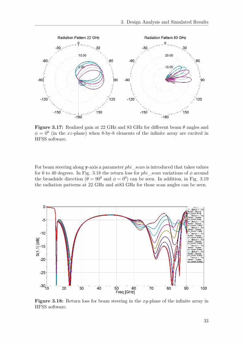
3.17 Realized gain at 22 GHz and 83 GHz for different beam θ angles andφ = 00 (in the xz-plane) when 8-by-8 elements of the infinite arrayare excited in HFSS software. . . . . . . . . . . . . . . . . . . . . . . 33
3.18 Return loss for beam steering in the xy-plane of the infinite array inHFSS software. . . . . . . . . . . . . . . . . . . . . . . . . . . . . . . 33
3.19 Realized gain at 22 GHz and 83 GHz for different beam φ angles andθ = 900 (in the xy-plane) when 8-by-8 elements of the infinite arrayare excited in HFSS software. . . . . . . . . . . . . . . . . . . . . . . 34
3.20 Structure’s reflection coefficient variation at 22 GHz for conductorand substrate thickness variation. Simulations made in HFSS. . . . . 35
3.21 Structure’s reflection coefficient variation at 73 GHz for conductorand substrate thickness variation. Simulations made in HFSS. . . . . 35
3.22 Structure’s reflection coefficient variation at 83 GHz for conductorand substrate thickness variation. Simulations made in HFSS. . . . . 36
3.23 Structure’s reflection coefficient variation at 22 GHz for feeding net-work dimensions variation. Simulations made in HFSS. . . . . . . . . 36
3.24 Structure’s reflection coefficient variation at 73 GHz for feeding net-work dimension variation. Simulations made in HFSS. . . . . . . . . 37
3.25 Structure’s reflection coefficient variation at 83 GHz for feeding net-work dimensions variation. Simulations made in HFSS. . . . . . . . . 37
3.26 Structure’s reflection coefficient variation at 22 GHz for element andcap dimensions variation. Simulations made in HFSS. . . . . . . . . . 38
3.27 Structure’s reflection coefficient variation at 73 GHz for element di-mensions variation. Simulations made in HFSS. . . . . . . . . . . . . 39
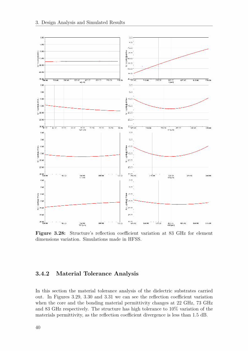
3.28 Structure’s reflection coefficient variation at 83 GHz for element di-mensions variation. Simulations made in HFSS. . . . . . . . . . . . . 40
3.29 Structure’s reflection coefficient variation at 22 GHz for material per-mittivity variation. Simulations made in HFSS. . . . . . . . . . . . . 41
3.30 Structure’s reflection coefficient variation at 73 GHz for material per-mittivity variation. Simulations made in HFSS. . . . . . . . . . . . . 41
3.31 Structure’s reflection coefficient variation at 83 GHz for material per-mittivity variation. Simulations made in HFSS. . . . . . . . . . . . . 41
xiv
List of Figures
4.1 2-by-1 dual polarization capped bow-tie sub-array prototype design. . 434.2 Transition from probe pad to element feeding via hole. . . . . . . . . 444.3 Transmission and reflection coefficients of the transition structure
seen in Fig. 4.2. . . . . . . . . . . . . . . . . . . . . . . . . . . . . . . 464.4 Return Loss of the two excited horizontal ports. A sub-array of 6-
by-7 dual polarization capped bow-tie elements, where only 2-by-1elements are excited. . . . . . . . . . . . . . . . . . . . . . . . . . . . 47
4.5 Return Loss of the two excited horizontal ports. A sub-array of 3-by-4 dual polarization capped bow-tie elements, where only 2-by-1elements are excited. . . . . . . . . . . . . . . . . . . . . . . . . . . . 48
4.6 Mutual coupling between horizontal ports. A sub-array of 6-by-7 dualpolarization capped bow-tie elements, where only 2-by-1 elements areexcited. . . . . . . . . . . . . . . . . . . . . . . . . . . . . . . . . . . 48
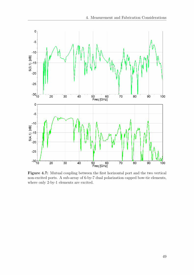
4.7 Mutual coupling between the first horizontal port and the two verticalnon-excited ports. A sub-array of 6-by-7 dual polarization cappedbow-tie elements, where only 2-by-1 elements are excited. . . . . . . . 49
xv

List of Figures
xvi

List of Tables
1.1 Specifications for class 3 antennas at PtP fixed radio systems [37]. . . 2
3.1 Laminate and bonding material properties. . . . . . . . . . . . . . . . 213.2 Optimized element design parameter values. . . . . . . . . . . . . . . 233.3 Common-mode resonant frequencies from adjacent feeding via holes. . 26
4.1 Optimized design parameter values for transition from probe pad toelement feeding via hole. . . . . . . . . . . . . . . . . . . . . . . . . . 45
xvii

List of Tables
xviii

1Introduction
1.1 Motivation
Wireless backhaul is the intermediate wireless communication infrastructure for con-nection between the smaller networks and the primary network, and it is of great im-portance for mobile network performance. As demands regarding mobile broadbandperformance are growing, new methods for higher spectrum efficiency are needed.
One of the methods is the Multiband Booster for backhaul, which is the Radio-link bonding (aggregation of carriers into a single virtual one) in different fre-quency bands, in order to achieve enhanced peak capacity, as well as higher effectivethroughput if statistical multiplexing is implemented. A bond between a wide highfrequency channel and a narrower low frequency one, will significantly improve theservice availability and guarantee higher capacity. When the high frequency signalwill be degraded due to propagation effects, such as rain, the low frequency willsecure the availability. Two potential band combinations are the bond between 18-42 GHz bands and E-band (70/80 GHz) for up to 5 km hops, and the bond between6-15 GHz bands and 8-48 GHz bands for longer hop distances [30].
In future heterogeneous networks, small cell layers will assist in handling trafficgrowth. Part of small cells, unable to access the wired backhaul, will be placedbetween street level and rooftop, and might neither have a clear line-of-sight (LOS)path to a macro site with backhaul. As the use of passive reflectors and repeaters toovercome this problem increases the cost, non line-of-sight (NLOS) backhaul may bethe solution. A research carried out by Ericsson showed how point-to-point (PtP)and point-to-multipoint (PtMP) microwave in licensed spectrum could be used forsmall cell NLOS backhaul [32].
Subsequently, there is great need to develop scalable solutions that will be able toadapt to technology evolution and needs, and at the same time provide lower costfor manufacturing and implementation. In terms of antennas, one proposed solutionis to use ultra-wideband dual polarization array antenna optimized to perform attwo different frequency bands, that will be used in a single radio unit.
1
1. Introduction
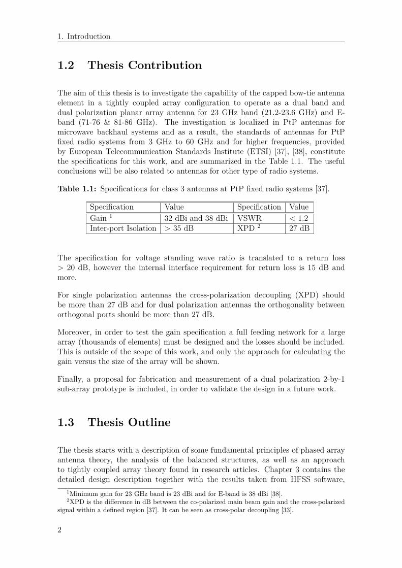
1.2 Thesis Contribution
The aim of this thesis is to investigate the capability of the capped bow-tie antennaelement in a tightly coupled array configuration to operate as a dual band anddual polarization planar array antenna for 23 GHz band (21.2-23.6 GHz) and E-band (71-76 & 81-86 GHz). The investigation is localized in PtP antennas formicrowave backhaul systems and as a result, the standards of antennas for PtPfixed radio systems from 3 GHz to 60 GHz and for higher frequencies, providedby European Telecommunication Standards Institute (ETSI) [37], [38], constitutethe specifications for this work, and are summarized in the Table 1.1. The usefulconclusions will be also related to antennas for other type of radio systems.
Table 1.1: Specifications for class 3 antennas at PtP fixed radio systems [37].
Specification Value Specification ValueGain 1 32 dBi and 38 dBi VSWR < 1.2Inter-port Isolation > 35 dB XPD 2 27 dB
The specification for voltage standing wave ratio is translated to a return loss> 20 dB, however the internal interface requirement for return loss is 15 dB andmore.
For single polarization antennas the cross-polarization decoupling (XPD) shouldbe more than 27 dB and for dual polarization antennas the orthogonality betweenorthogonal ports should be more than 27 dB.
Moreover, in order to test the gain specification a full feeding network for a largearray (thousands of elements) must be designed and the losses should be included.This is outside of the scope of this work, and only the approach for calculating thegain versus the size of the array will be shown.
Finally, a proposal for fabrication and measurement of a dual polarization 2-by-1sub-array prototype is included, in order to validate the design in a future work.
1.3 Thesis Outline
The thesis starts with a description of some fundamental principles of phased arrayantenna theory, the analysis of the balanced structures, as well as an approachto tightly coupled array theory found in research articles. Chapter 3 contains thedetailed design description together with the results taken from HFSS software,
1Minimum gain for 23 GHz band is 23 dBi and for E-band is 38 dBi [38].2XPD is the difference in dB between the co-polarized main beam gain and the cross-polarized
signal within a defined region [37]. It can be seen as cross-polar decoupling [33].
2

1. Introduction
as well as some problems and some solutions to meet the specifications. Chapter3 concludes with the dimension tolerance analysis of the structure. The prototypeproposal and description is mentioned in Chapter 4. Finally, in Chapter 5 the readercan find the conclusion of this thesis and some suggestions for future work.
3

1. Introduction
4
2Theory
In the following sections, the phased array antenna theory is shown, focusing onthe principles that are important for this work. It is advised that the reader shouldlook for the entire theory in [33] and [34], as the intention of this work is not to giveall the meanings and the important derivations around antenna theory, but only toshow the ones behind the simulations that carried out.
2.1 Planar Phased Array Antennas
An array is a collection of elements integrated within one module that includes asignal distribution network. In planar arrays the elements are located in a planar 2Dgrid in an optimal way to achieve enhanced performance compared to single elementantennas. One of main advantages of the array configuration is the possibility ofbeam shaping, having narrower beam-width that provides higher gain, transmissionin longer distances or lower transmitted power.
Moreover, arrays can also be used for beam scanning or even for transmission withmultiple beams, as well as the side lobe position and level can be controlled. On theother hand, the cost may be higher, depending on the design. Design and fabricationof arrays are more complicated, compared to horn and reflector antennas.
The radiation pattern (the shape of the levels of radiation in space) of regular arrayscan be determined by the following parameters that must be taken into accountduring the design process:
• The grid geometry
• The distance between the elements (known as Element Spacing)
• The amplitude and the phase of the excitation of each element
5

2. Theory
2.1.1 Radiation Fields
According to electromagnetic radiation theory for single elements located in freespace, the radiated field at a point r with distance and direction r = r/r in thefar-field is described by [33]:
E(r) = G(r)ejkr/r ⇐⇒ E(r, θ, φ) = G(θ, φ)ejkr/r (2.1)
where G(r) is a function of amplitude and phase of the field with direction, andk is the wave number. The far-field (or Fraunhofer) is the region that satisfiesr ≥ 2D2/λ, where D is the largest antenna dimension. In this region the radiatedfield waves are considered planar and the radiation pattern’s shape remains constantwith distance.
Figure 2.1: Rectangular grid with positions of the elements of the planar array.
For a planar array of equal and equally spaced N by M elements placed in xy- planeas in Fig. 2.1, the radiated field of the nmth element for unit amplitude at a pointr is described as [33]:
Enm(r) = 1rejkrG(r)ejkRnm·r (2.2)
where Rnm is the reference point of each element and for n=1,2,. . . ,N, m=1,2,. . . ,Mcan be written as:
6
2. Theory
Rnm = Rc + (n− N + 12 )dxx + (m− M + 1
2 )dyy (2.3)
The geometrical center of the planar array is Rc and dx, dy are the element spacing(distance between adjacent elements) in each direction. The amplitude and thephase of the current excitation of the nmth element are Anm and Φnm respectively,so after the summation for all the elements the far-field function of the whole arraycan be written as [33]:
GA(r) =N∑n=1
M∑m=1
AnmejΦnmG(r)ejkRnm·r = G(r)AF(r) (2.4)
where G(r) is the far-field function of the embedded element and AF(r) is the arrayfactor [33]:
AF(r) =N∑n=1
M∑m=1
AnmejΦnmejkRnm·r (2.5)
2.1.2 Grating Lobes
Assuming a smooth and continuous planar phase function of the current excitation:
Φ(x, y) = Φc − kΦxx− kΦyy (2.6)
the propagation constants in x and y direction can be written as:
kΦx = −∆Φx/dx with − π < ∆Φx < πkΦy = −∆Φy/dy with − π < ∆Φy < π
(2.7)
The location of the grating lobes can be found through the maximum values of thearray factor:
Kxp = kΦx + p2πdx, p = ±1,±2, . . . ,
Kyq = kΦy + p2πdy, q = ±1,±2, . . . ,
(2.8)
and if the uv - coordinates are used (u = sin θ cosφ and v = sin θ sinφ ), where kx/k= sinθ cosφ and ky/k = sinθ sinφ, Eq. 2.8 becomes:
7
2. Theory
sin θpq cosφpq = sin θ0 cosφ0 + pλ
dx
sin θpq sinφpq = sin θ0 sinφ0 + qλ
dy
(2.9)
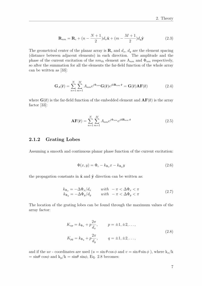
The location of the grating lobes can be represented in a rectangular grid in uv-plane, as seen in Fig. 2.2 (a). The total radiation pattern that includes both themain lobe and the grating lobes, is determined by the visible space, which is definedas the area that satisfies | sin θ| ≤ 1 and is represented by the circle in Fig. 2.2 (b).
Figure 2.2: (a) Array factor with main and grating lobes, (b) Total radiationpattern [33].
In order to satisfy the requirement for no grating lobes, we can either make surethat they are located outside the visible space, or that they are suppressed by theelement pattern. The former is achieved when sin θpq > 1 + λ/D for all pq, whereD is the is the diameter of the array in the φ-plane, which corresponds to:
√√√√(sin θ0 cosφ0 + pλ
dx+ sin θ0 sinφ0 + q
λ
dy
)2
> 1 + λ
D(2.10)
Therefore, for broadside transmission (at z direction for θ, φ = 0 according to Fig.2.2) the sufficient condition for non-radiating grating lobes becomes [33]:
dx ≤λ
1 + λ/D
dy ≤λ
1 + λ/D
(2.11)
8

2. Theory
2.1.3 Steering Main Lobe
An array antenna is able to steer the main beam in a specific direction rs = rs/rs,or (θs, φs). This can be accomplished by exciting the elements along the vector ofsteered beam with a linearly progressive phase, while the amplitude is uniform [33].In this case the array factor becomes:
AF(r) =N∑n=1
M∑m=1
AnmejΦnmejkRnm·rejkRnm·rs (2.12)
When δx, δy are the phase difference between two adjacent elements in x, y directionrespectively, that are calculated for a specific beam direction, and for
ξ = kdx cosφ sin θ + δx = kdxu+ δx
η = kdy sinφ sin θ + δy = kdyv + δy
(2.13)
the array factor becomes:
AF = AnmN∑n=1
ejnξM∑m=1
ejmη ⇐⇒ |AF| =
∣∣∣∣∣∣∣∣sin Nξ2N sin ξ2
∣∣∣∣∣∣∣∣∣∣∣∣∣∣∣∣sin Mη
2M sin η2
∣∣∣∣∣∣∣∣ (2.14)
2.1.4 Polarization
The polarization of an electromagnetic wave is determined by the characteristicsof the electric field (or E-field). The E-field can have both x- and y- components(assuming propagation at z direction), so two different signals at the same frequencycan be modulated at the same time in order to double the capacity of the trans-mission, as long as the fields form a pair of orthogonal polarizations. Orthogonalityprovides high isolation between the two polarizations as well as low mutual interfer-ence. In linear polarization, one component is referred as horizontal (HOR) and theother as vertical (V ER), both relative to the ground. When for example the antennatransmits and receives using the horizontal polarization, the isolation is defined asthe ratio between the horizontal and vertical components of E-field. One method totest the isolation is to calculate the cross-polar decoupling [33]:
(XPD)dB = 10log10
∣∣∣∣∣EcoExp
∣∣∣∣∣2
(2.15)
9
2. Theory
where co = ˆHOR and xp = ˆVER for the above example. XPD can also befound as cross-polar discrimination and the specification regarding XPD for singlepolarization PtP antennas is 27 dB [37].
In dual polarization antennas when both polarizations are desirable, one is interestedto see how much parallel are the two orthogonal polarizations in terms of E-fieldvectors. One method to test the orthogonality is to calculate the PolarizationParallelity, by exciting both polarizations one at a time, and each time measurethe E-field vector in the direction of the excitation. Then the measured E-fieldvectors are divided by their magnitude to become unit vectors and compared bytaking their product:
ρ = EHOR(θ, φ) · EV ER(θ, φ)∗∣∣∣EHOR(θ, φ)∣∣∣ ∣∣∣EV ER(θ, φ)
∣∣∣ (2.16)
where Ei = Eiθθ + Ei
φφ for i = HOR or V ER is the electrical field vector at thefar-field when horizontal and when vertical polarization is excited respectively.
In this work the antenna radiates at z direction so in Eq. 2.16 angle θ is zero. Whenthe two polarizations are orthogonal to each other the Eq. 2.16 gives ρ = 0, whereasif they are parallel it gives ρ = 1. It is convenient to take the logarithm of 1 − ρ,which is the Polarization Orthogonality, and compare it with the level in dB ofXPD. We can assume that the specification for polarization parallelity is the sameas for XPD (it is not clearly specified from ETSI for dual band antennas).
2.1.5 Directivity
Directivity is defined as the maximum value of the directivity function at the di-rection of interest. In simple words, it provides an indication of the ability of theantenna to concentrate the beam in a specific direction. So one can use the formula[33]:
D = 4π |G(θ0, φ0)AF(θ0, φ0) · co∗|2
P= egrtepoleill cos θ0Dmax (2.17)
where P is the power integral of the planar array:
P =∫ 2π
0
∫ 2π
0|GA(θ, φ)| sin θ dθdφ (2.18)
where GA(θ, φ) is the far-field function of the array. The factors in the second partof the equation are the maximum available directivity:
10

2. Theory
Dmax = 4πλ2NAcell N : number of elements
Acell : element aperture area(2.19)
the illumination efficiency:
eill = 1NAcell
∣∣∣∣∫∫AA(x, y) dxdy
∣∣∣∣2 / ∫∫A|A(x, y)|2 dxdy (2.20)
the polarization efficiency:
epol = |G(θ0, φ0) · co∗|2 /(|G(θ0, φ0) · co∗|2 + |G(θ0, φ0) · xp∗|2
)(2.21)
and the grating efficiency:
egrt = |G(θ0, φ0)|2 /(∑pq
|G(θpq, φpq)|2cos θ0
cos θpq
)(2.22)
2.1.6 Array Gain
The realized gain Garray of a passive array with equally spaced and equal elementsize and shape can be found if the second part of the equation 2.17 is multiplied bythe radiation efficiency erad, which is the ratio between the radiated and the incidentpower. So the realized gain can be expressed as [33]:
Garray = eradegrtepoleill cos θ0Dmax (2.23)
In the Eq. 2.23 the array realized gain increases linearly with the number of elements.When the number of elements are small the feeding network losses are not too large,so the gain continues to increase with size. However, the gain is ultimately limited ifthe losses are not negligible. For a planar array of N elements with element spacingd in both directions and transmission lines with length (N1/2−1)d, the realized gainat broadside when all elements are assumed matched is given by [34]:
Garray = eradegrtepoleill4πλ2NAcell10−(d/λ)(N1/2−1)(adB/λ/10) (2.24)
where adB/λ is the loss of the transmission line in decibels per wavelength due toattenuation, and Acell is the aperture area of a single element. In order to be moreprecise, the losses due to power divider need to be added for the total losses.
11
2. Theory
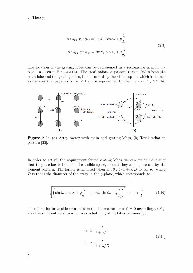
Figure 2.3: Gain limitation with line losses at 86 GHz for eradegrtepoleill = 1.
In Fig. 2.3 we can see the gain in dBi versus the number of elements in a planararray for different transmission line losses at 86 GHz. For this scenario it is assumedthat illumination, polarization, grating and radiation efficiency are one (ideal case).In addition, the element spacing is 1.894 mm in both directions as this is the valuethat used in the simulations of this work. It is obvious that the maximum achievablegain saturation depends on the line losses of the feeding network.
Figure 2.4: Gain limitation with line losses at 21 GHz for eradegrtepoleill = 1.
12
2. Theory
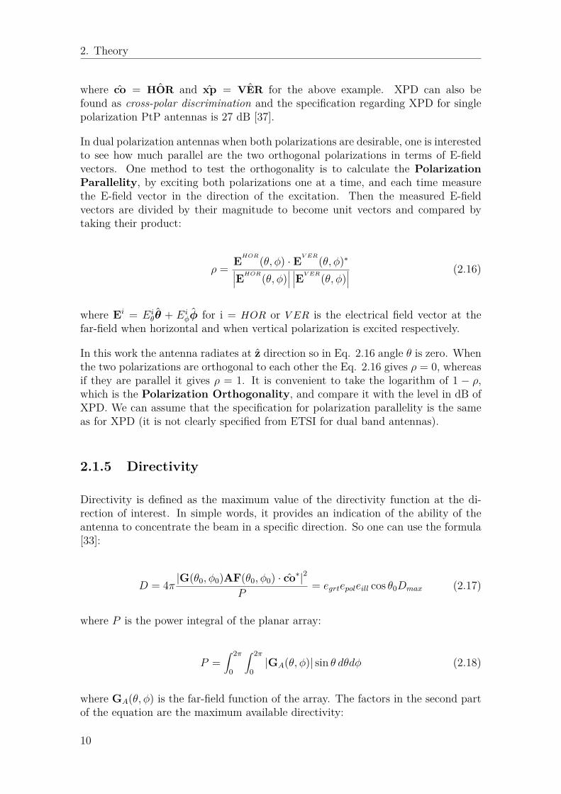
In Fig. 2.4 we can see the gain limitation for 21 GHz under the same assumptions.It is observed that the maximum gain is at the same level as in 86 GHz and withthe same element spacing more elements required to achieve that gain.
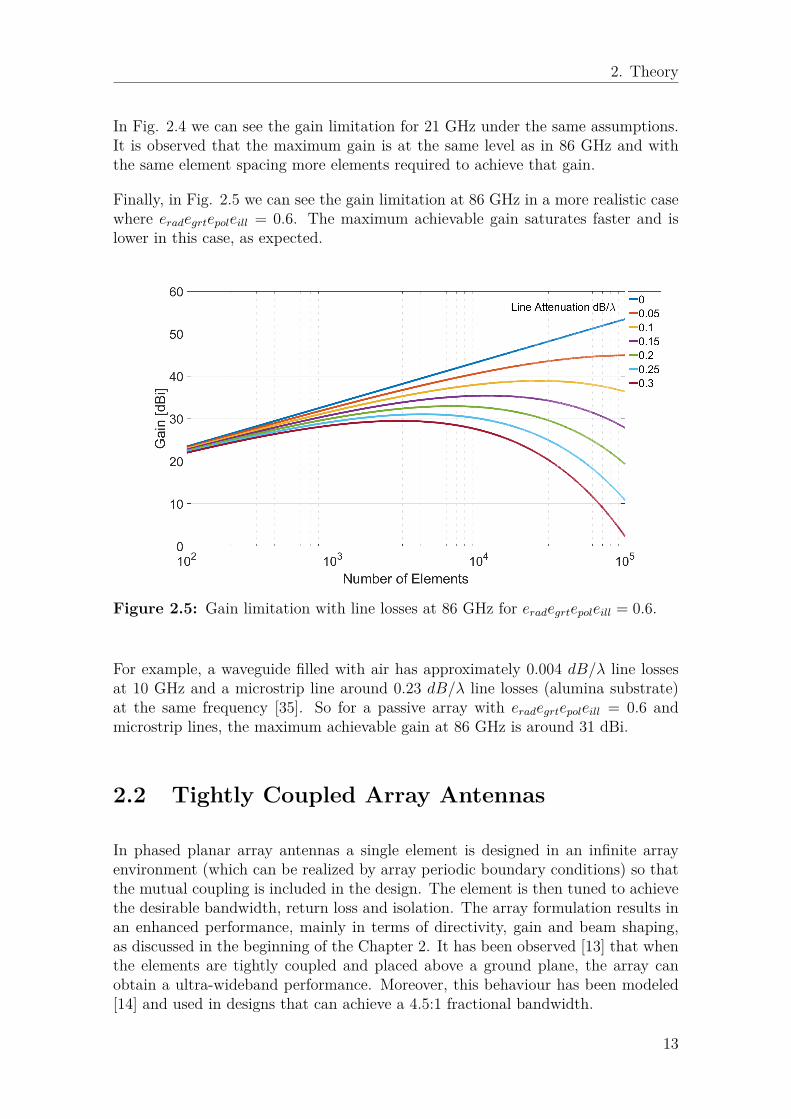
Finally, in Fig. 2.5 we can see the gain limitation at 86 GHz in a more realistic casewhere eradegrtepoleill = 0.6. The maximum achievable gain saturates faster and islower in this case, as expected.
Figure 2.5: Gain limitation with line losses at 86 GHz for eradegrtepoleill = 0.6.
For example, a waveguide filled with air has approximately 0.004 dB/λ line lossesat 10 GHz and a microstrip line around 0.23 dB/λ line losses (alumina substrate)at the same frequency [35]. So for a passive array with eradegrtepoleill = 0.6 andmicrostrip lines, the maximum achievable gain at 86 GHz is around 31 dBi.
2.2 Tightly Coupled Array Antennas
In phased planar array antennas a single element is designed in an infinite arrayenvironment (which can be realized by array periodic boundary conditions) so thatthe mutual coupling is included in the design. The element is then tuned to achievethe desirable bandwidth, return loss and isolation. The array formulation results inan enhanced performance, mainly in terms of directivity, gain and beam shaping,as discussed in the beginning of the Chapter 2. It has been observed [13] that whenthe elements are tightly coupled and placed above a ground plane, the array canobtain a ultra-wideband performance. Moreover, this behaviour has been modeled[14] and used in designs that can achieve a 4.5:1 fractional bandwidth.
13
2. Theory
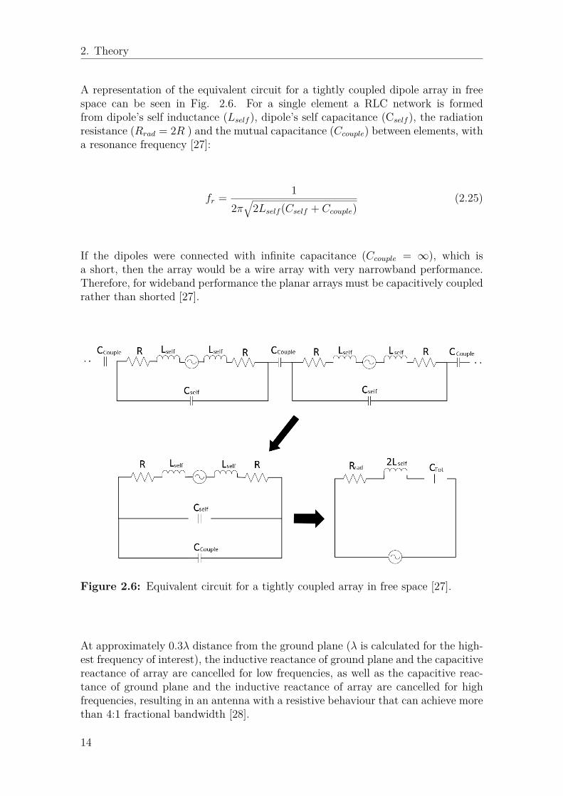
A representation of the equivalent circuit for a tightly coupled dipole array in freespace can be seen in Fig. 2.6. For a single element a RLC network is formedfrom dipole’s self inductance (Lself ), dipole’s self capacitance (Cself ), the radiationresistance (Rrad = 2R ) and the mutual capacitance (Ccouple) between elements, witha resonance frequency [27]:
fr = 12π√
2Lself (Cself + Ccouple)(2.25)
If the dipoles were connected with infinite capacitance (Ccouple = ∞), which isa short, then the array would be a wire array with very narrowband performance.Therefore, for wideband performance the planar arrays must be capacitively coupledrather than shorted [27].
Figure 2.6: Equivalent circuit for a tightly coupled array in free space [27].
At approximately 0.3λ distance from the ground plane (λ is calculated for the high-est frequency of interest), the inductive reactance of ground plane and the capacitivereactance of array are cancelled for low frequencies, as well as the capacitive reac-tance of ground plane and the inductive reactance of array are cancelled for highfrequencies, resulting in an antenna with a resistive behaviour that can achieve morethan 4:1 fractional bandwidth [28].
14

2. Theory
Figure 2.7: (Top) Equivalent circuit for an array in free space. (Bottom) Equiva-lent circuit for an array with a ground plane [27].
In order to understand the effect of the ground plane one can refer to equivalentcircuit that can be seen in Fig. 2.7. The top sub-figure illustrates the circuitrepresentation of an ideal array in free space, where the elements are electricallysmall with absence of grating lobes making the circuit valid. Assuming that the twohalf spaces have characteristic impedance 2RA0, the input impedance of the arraybecomes (the symbols are kept the same as the reference article for simplicity) [27]:
ZA = RA0 + jXA0 (2.26)
where XA0 is the array reactance. In the bottom sub-figure the ground plane hasbeen inserted, which has an impedance from transmission line theory [35]:
Zgp = 2RA0(ZL + 2RA0 tanβd)/(2RA0 + ZL tanβd) (2.27)
So the input impedance of the array becomes [27]:
ZA = 2RA0//Zgp + jXA0 (2.28)
As a result, the Eq. 2.28 obtains two solutions, which can be represented in SmithChart where the curve of ZA gets a second passage from the center [27].
In conclusion, a good interpretation of the behaviour of this technology can be sum-marized with the phrase of Moulder et al. [20], “Tightly coupled arrays (TCAs)act as “meta-structured” apertures rather than arrays of discrete ele-ments”. Recent work in the field of TCA technology can be found in [14], [17], [18],[19], [20] and [21].
15
2. Theory
2.3 Balance to Unbalance Feeding Structures
In a “balanced” connection between two circuits or between two devices, the signalis between two terminals - conductors that have the same impedance to ground. Ina proper balanced connection, a balanced output must be connected to a differentialinput, where the two conductors transmit the same signal with opposite polarity.
Many types of antennas, for example dipole or bow-tie antennas, have a differentialinput and require a transformer before them in order to be connected with a circuitthat has a single-ended signal as output. Those transformers, which are calledbaluns (balance-to-unbalance), are very important elements for the performance ofthe antenna and usually are the limiting factors in terms of bandwidth, losses, spacerequirements and cost.
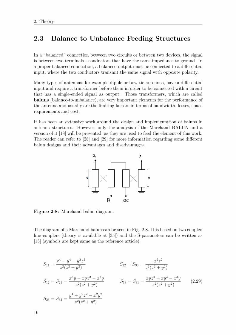
It has been an extensive work around the design and implementation of baluns inantenna structures. However, only the analysis of the Marchand BALUN and aversion of it [18] will be presented, as they are used to feed the element of this work.The reader can refer to [28] and [29] for more information regarding some differentbalun designs and their advantages and disadvantages.
Figure 2.8: Marchand balun diagram.
The diagram of a Marchand balun can be seen in Fig. 2.8. It is based on two coupledline couplers (theory is available at [35]) and the S-parameters can be written as[15] (symbols are kept same as the reference article):
S11 = x4 − y4 − y2z2
z2(z2 + y2) S22 = S33 = −x2z2
z2(z2 + y2)
S12 = S21 = x3y − xyz2 − x3y
z2(z2 + y2) S13 = S31 = xyz2 + xy3 − x3y
z2(z2 + y2)
S23 = S32 = y4 + y2z2 − x2y2
z2(z2 + y2)
(2.29)
16
2. Theory
where x =√
1− k2, y = jk sin θ and z =√
1− k2 cos θ + j sin θ, k is the couplingcoefficient between the coupled lines and θ is the electrical length [15]. The mostimportant performance characteristics of the balun that should be taken into accountduring design process are following:
• Frequency Range
• Amplitude & Phase Balance - How close to equal power and 1800 phasedifference are the output signals.
• Common Mode Rejection Ratio - Total common-mode signal attenua-tion/rejection.
• Return Loss - The ratio of the signal reflected back from a device under test,to the signal inserted to that device.
• Impedance Ratio - The ratio of unbalanced impedance to balanced impedance.
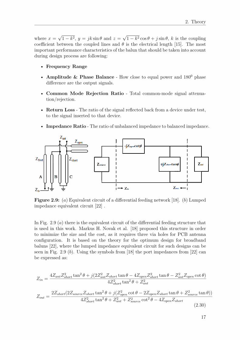
Figure 2.9: (a) Equivalent circuit of a differential feeding network [18]. (b) Lumpedimpedance equivalent circuit [22] .
In Fig. 2.9 (a) there is the equivalent circuit of the differential feeding structure thatis used in this work. Markus H. Novak et al. [18] proposed this structure in orderto minimize the size and the cost, as it requires three via holes for PCB antennaconfiguration. It is based on the theory for the optimum design for broadbandbaluns [22], where the lumped impedance equivalent circuit for such designs can beseen in Fig. 2.9 (b). Using the symbols from [18] the port impedances from [22] canbe expressed as:
Zin = 4ZantZ2short tan2 θ + j(2Z2
antZshort tan θ − 4ZopenZ2short tan θ − Z2
antZopen cot θ)4Z2
short tan2 θ + Z2ant
Zout =2Zshort(2ZsourceZshort tan2 θ + j(Z2
open cot θ − 2ZopenZshort tan θ + Z2source tan θ))
4Z2short tan2 θ + Z2
ant + Z2source cot2 θ − 4ZopenZshort
(2.30)
17
2. Theory
where θ is the electrical length of the short-circuit. If the designed balun satisfiesthe Zshort >> Zopen condition then it obtain ultra-wideband (UWB) performance[18].
2.4 UWB Antenna Research Activities at ChalmersUniversity of Technology
The Antenna Group at Chalmers University of Technology has been developingseveral UWB antennas. Some of the work that has been done and is still carried outis the hat-feed reflector antenna, which is a kind of wideband antenna [1-6] that canbe applied in satellite communication systems. The self-grounded bow-tie antenna[7-11] is another kind of UWB antenna and it can be applied under many scenarios,for instance, UWB radar and medical detection. Finally, the quad-ridge horn is anUWB antenna [12] applied mainly in radio telescopes.
18
3Design Analysis and Simulated
Results
In the following sections, the dual polarization capped bow-tie array antenna designis analyzed and the results from simulations are then discussed.
3.1 Dual Polarization Capped Bow-Tie TCA
3.1.1 Dual Polarization Bow-Tie Element
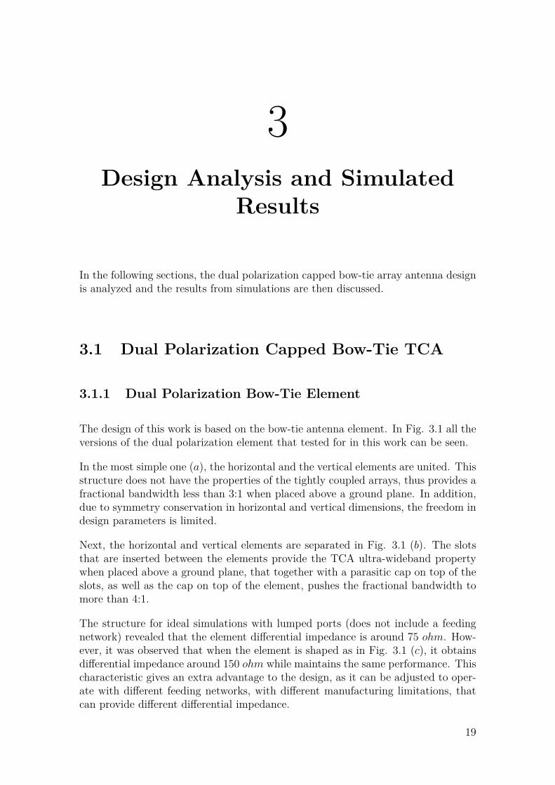
The design of this work is based on the bow-tie antenna element. In Fig. 3.1 all theversions of the dual polarization element that tested for in this work can be seen.
In the most simple one (a), the horizontal and the vertical elements are united. Thisstructure does not have the properties of the tightly coupled arrays, thus provides afractional bandwidth less than 3:1 when placed above a ground plane. In addition,due to symmetry conservation in horizontal and vertical dimensions, the freedom indesign parameters is limited.
Next, the horizontal and vertical elements are separated in Fig. 3.1 (b). The slotsthat are inserted between the elements provide the TCA ultra-wideband propertywhen placed above a ground plane, that together with a parasitic cap on top of theslots, as well as the cap on top of the element, pushes the fractional bandwidth tomore than 4:1.
The structure for ideal simulations with lumped ports (does not include a feedingnetwork) revealed that the element differential impedance is around 75 ohm. How-ever, it was observed that when the element is shaped as in Fig. 3.1 (c), it obtainsdifferential impedance around 150 ohm while maintains the same performance. Thischaracteristic gives an extra advantage to the design, as it can be adjusted to oper-ate with different feeding networks, with different manufacturing limitations, thatcan provide different differential impedance.
19
3. Design Analysis and Simulated Results
Finally, in Fig. 3.1 (d) one extra design parameter is inserted, providing one morefreedom for better fine tuning.
Figure 3.1: Progress of dual polarization capped bow-tie element. In the 2-by-1sub-arrays that are shown the caps (hexagonal copper structures) have been removedfrom figure for better view of the element, as well as the feeding parts. (a) Firstdesign, (b) Slotted element, (c) Slotted and shaped element, (d) Slotted elementwith extra design freedom.
3.1.2 Analysis of Dual Polarization Capped Bow-Tie TCA
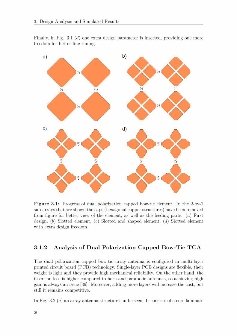
The dual polarization capped bow-tie array antenna is configured in multi-layerprinted circuit board (PCB) technology. Single-layer PCB designs are flexible, theirweight is light and they provide high mechanical reliability. On the other hand, theinsertion loss is higher compared to horn and parabolic antennas, so achieving highgain is always an issue [36]. Moreover, adding more layers will increase the cost, butstill it remains competitive.
In Fig. 3.2 (a) an array antenna structure can be seen. It consists of a core laminate
20

3. Design Analysis and Simulated Results
(the “green” layer) that has the ground plane on the bottom side and the elementon the top side. On the top of that, a bonding material follows (the middle “yellow”layer), having the parasitic caps (hexagonal copper structure) and the feeding stubson top. The properties of the substrates used are summarized in Table 3.1.
Figure 3.2: (a) Multi-layer PCB design of a 4-by-4 sub-array. (b) Substrate designparameters, feeding network included.
Notice that in this layer only the four feeding stubs are shown. Finally, an extrabonding material follows, which has the caps (hexagonal copper structure) on top.In Fig. 3.2 (b) the side view of the structure can be seen, together with the via holesthat are part of the feeding network.
Table 3.1: Laminate and bonding material properties.
Manufacturer Material Permitivity Loss TangentRogers RT/duriod 5880 2.2 0.0009Taconic Fast Rise 27 2.7 0.0014TUC TU-933P 1 3.4 0.0025
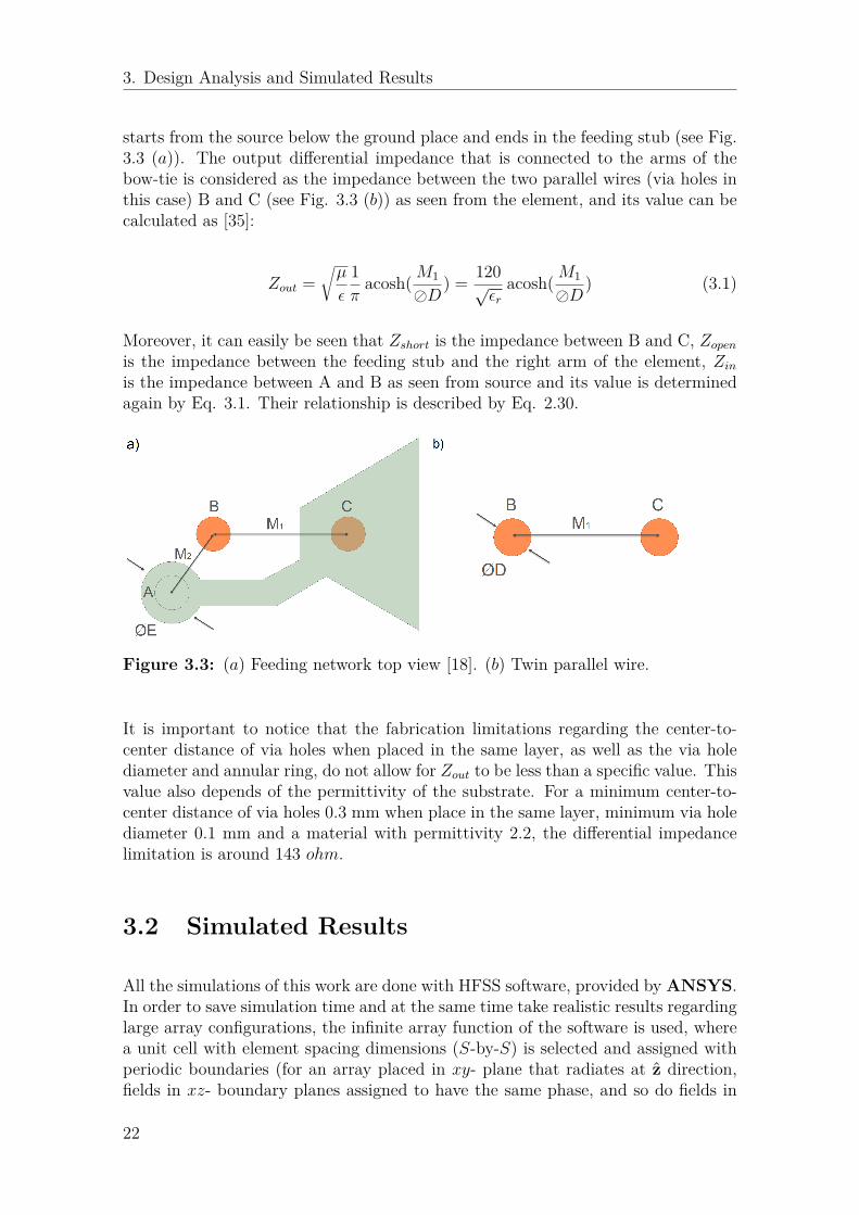
3.1.3 Feeding Structure
The feeding structure that is used in this work, is the one that introduced by Novaket al. [18] and its principles were discussed in Chapter 2. The structure consistsof three via holes, two that connect each arm with the ground plane and one that
1TU-933P will be used for measurement purposes that will be seen in Chapter 4
21
3. Design Analysis and Simulated Results
starts from the source below the ground place and ends in the feeding stub (see Fig.3.3 (a)). The output differential impedance that is connected to the arms of thebow-tie is considered as the impedance between the two parallel wires (via holes inthis case) B and C (see Fig. 3.3 (b)) as seen from the element, and its value can becalculated as [35]:
Zout =õ
ε
1π
acosh( M1
�D) = 120√εr
acosh( M1
�D) (3.1)
Moreover, it can easily be seen that Zshort is the impedance between B and C, Zopenis the impedance between the feeding stub and the right arm of the element, Zinis the impedance between A and B as seen from source and its value is determinedagain by Eq. 3.1. Their relationship is described by Eq. 2.30.
Figure 3.3: (a) Feeding network top view [18]. (b) Twin parallel wire.
It is important to notice that the fabrication limitations regarding the center-to-center distance of via holes when placed in the same layer, as well as the via holediameter and annular ring, do not allow for Zout to be less than a specific value. Thisvalue also depends of the permittivity of the substrate. For a minimum center-to-center distance of via holes 0.3 mm when place in the same layer, minimum via holediameter 0.1 mm and a material with permittivity 2.2, the differential impedancelimitation is around 143 ohm.
3.2 Simulated Results
All the simulations of this work are done with HFSS software, provided by ANSYS.In order to save simulation time and at the same time take realistic results regardinglarge array configurations, the infinite array function of the software is used, wherea unit cell with element spacing dimensions (S-by-S) is selected and assigned withperiodic boundaries (for an array placed in xy- plane that radiates at z direction,fields in xz- boundary planes assigned to have the same phase, and so do fields in
22

3. Design Analysis and Simulated Results
yz- boundary planes). Moreover, a floquet port is assigned in xy- plane at the topinstead of a radiation boundary. In Fig. 3.4 the capped bow-tie array structure canbe seen.
The simulations started with the absence of the balun. A lumped port is used soas to tune the element and achieve the best performance that it could provide in“ideal” situation.
Figure 3.4: Design parameters of dual polarization capped bow-tie. (a) Element,(b) Parasitic Cap, (c) Cap, (d) Feeding Stub.
The balun is added afterwards and the whole structure is tuned again, having the“ideal” situation as the target. In order to visualize the radiation patterns in 23 GHzband, more elements apart from the unit cell needs to be excited for larger aperturearea. For that purposed in the infinite array 8-by-8 elements are exited (the arraymodel function is provided by the software). The design parameter values afteroptimization for best return loss and used for all the figures of this Chapter aresummarized in Table 3.2. This work follows the design rules found in [31].
Table 3.2: Optimized element design parameter values.
Parameter (mm) Parameter (mm) Parameter (mm)W1 0.15 S 1.894 M1 0.22W2 0.6 a 0.5 M2 0.39L1 0.38 b 0.163 H1 1.03L2 0.15 c 0.5 H2 0.073L3 0.3 d 0.226 H3 0.357L4 0.124 F1 0.346 � D 0.1G 0.11 F2 0.558 � E 0.2
23
3. Design Analysis and Simulated Results
3.2.1 Return Loss and Isolation
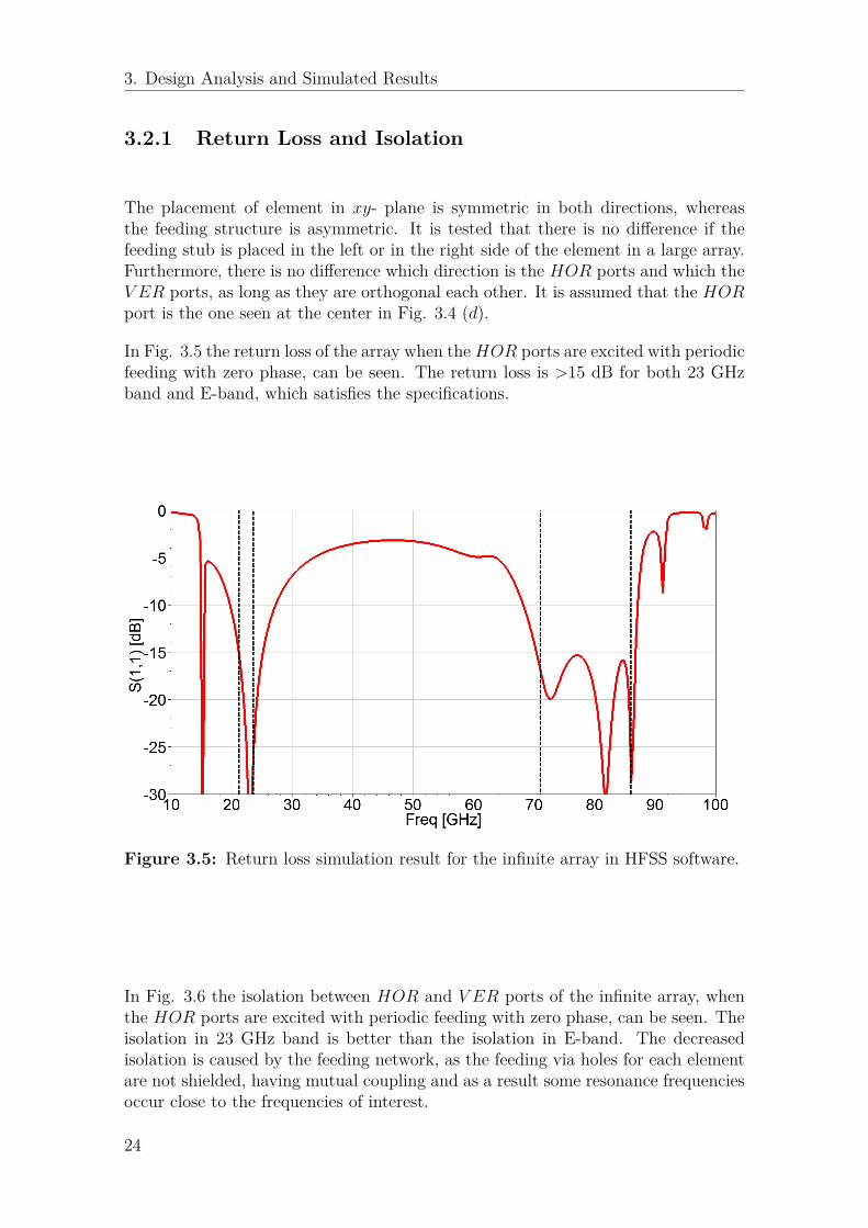
The placement of element in xy- plane is symmetric in both directions, whereasthe feeding structure is asymmetric. It is tested that there is no difference if thefeeding stub is placed in the left or in the right side of the element in a large array.Furthermore, there is no difference which direction is the HOR ports and which theV ER ports, as long as they are orthogonal each other. It is assumed that the HORport is the one seen at the center in Fig. 3.4 (d).
In Fig. 3.5 the return loss of the array when theHOR ports are excited with periodicfeeding with zero phase, can be seen. The return loss is >15 dB for both 23 GHzband and E-band, which satisfies the specifications.
Figure 3.5: Return loss simulation result for the infinite array in HFSS software.
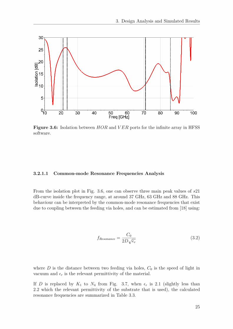
In Fig. 3.6 the isolation between HOR and V ER ports of the infinite array, whenthe HOR ports are excited with periodic feeding with zero phase, can be seen. Theisolation in 23 GHz band is better than the isolation in E-band. The decreasedisolation is caused by the feeding network, as the feeding via holes for each elementare not shielded, having mutual coupling and as a result some resonance frequenciesoccur close to the frequencies of interest.
24
3. Design Analysis and Simulated Results
Figure 3.6: Isolation between HOR and V ER ports for the infinite array in HFSSsoftware.
3.2.1.1 Common-mode Resonance Frequencies Analysis
From the isolation plot in Fig. 3.6, one can observe three main peak values of s21dB-curve inside the frequency range, at around 37 GHz, 63 GHz and 88 GHz. Thisbehaviour can be interpreted by the common-mode resonance frequencies that existdue to coupling between the feeding via holes, and can be estimated from [18] using:
fResonance = C0
2D√εr(3.2)
where D is the distance between two feeding via holes, C0 is the speed of light invacuum and εr is the relevant permittivity of the material.
If D is replaced by K1 to N4 from Fig. 3.7, when εr is 2.1 (slightly less than2.2 which the relevant permittivity of the substrate that is used), the calculatedresonance frequencies are summarized in Table 3.3.
25

3. Design Analysis and Simulated Results
Figure 3.7: Distance between adjacent feeding via holes that cause common-moderesonant frequencies.
The frequencies where the three main peak values of dB(S21) curve (Fig. 3.6) occur,are related to N1 to N4, K2 and K3 distances respectively. With careful tuning ofthe feeding network, the isolation can be improved to a certain level. However, anydistance changes that are related to the feeding network affect the output impedanceof the structure and as a result the return loss. Therefore, when tuning the feedingnetwork it is necessary to observe isolation and return loss changes at the same time.
Table 3.3: Common-mode resonant frequencies from adjacent feeding via holes.
Parameter Frequency Parameter FrequencyK1 57.5 GHz N1 31.3 GHzK2 62.5 GHz N2 33.7 GHzK3 88.3 GHz N3 34.4 GHzK4 111.5 GHz N4 37.7 GHz
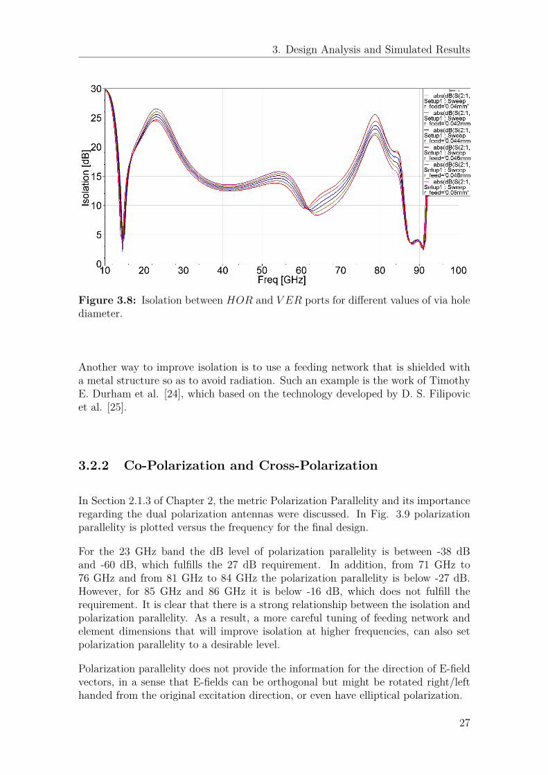
Moreover, there is a relationship between the isolation and the via hole diameter.From Fig. 3.8 it is observed that for thinner via hole the isolation slightly improvesat E-band, but becomes worse for 23 GHz band. Again, via hole diameter changesaffect the output impedance of the structure and as a consequence the return loss.
26
3. Design Analysis and Simulated Results
Figure 3.8: Isolation between HOR and V ER ports for different values of via holediameter.
Another way to improve isolation is to use a feeding network that is shielded witha metal structure so as to avoid radiation. Such an example is the work of TimothyE. Durham et al. [24], which based on the technology developed by D. S. Filipovicet al. [25].
3.2.2 Co-Polarization and Cross-Polarization
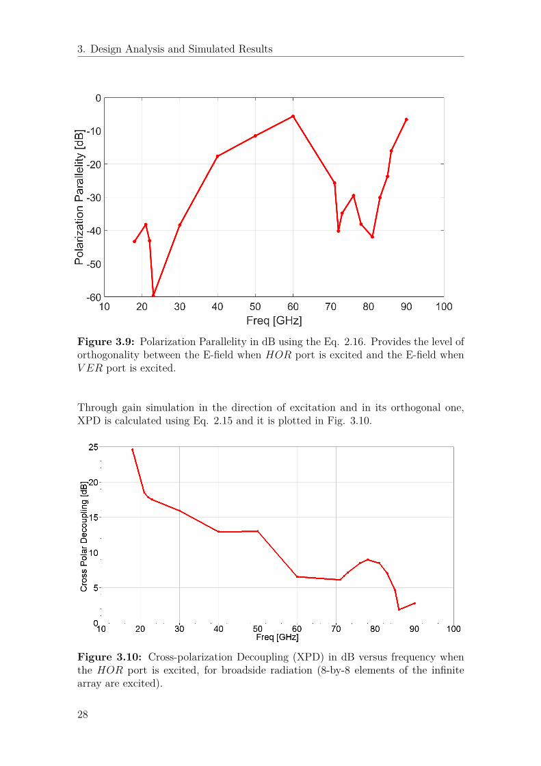
In Section 2.1.3 of Chapter 2, the metric Polarization Parallelity and its importanceregarding the dual polarization antennas were discussed. In Fig. 3.9 polarizationparallelity is plotted versus the frequency for the final design.
For the 23 GHz band the dB level of polarization parallelity is between -38 dBand -60 dB, which fulfills the 27 dB requirement. In addition, from 71 GHz to76 GHz and from 81 GHz to 84 GHz the polarization parallelity is below -27 dB.However, for 85 GHz and 86 GHz it is below -16 dB, which does not fulfill therequirement. It is clear that there is a strong relationship between the isolation andpolarization parallelity. As a result, a more careful tuning of feeding network andelement dimensions that will improve isolation at higher frequencies, can also setpolarization parallelity to a desirable level.
Polarization parallelity does not provide the information for the direction of E-fieldvectors, in a sense that E-fields can be orthogonal but might be rotated right/lefthanded from the original excitation direction, or even have elliptical polarization.
27
3. Design Analysis and Simulated Results
Figure 3.9: Polarization Parallelity in dB using the Eq. 2.16. Provides the level oforthogonality between the E-field when HOR port is excited and the E-field whenV ER port is excited.
Through gain simulation in the direction of excitation and in its orthogonal one,XPD is calculated using Eq. 2.15 and it is plotted in Fig. 3.10.
Figure 3.10: Cross-polarization Decoupling (XPD) in dB versus frequency whenthe HOR port is excited, for broadside radiation (8-by-8 elements of the infinitearray are excited).
28
3. Design Analysis and Simulated Results
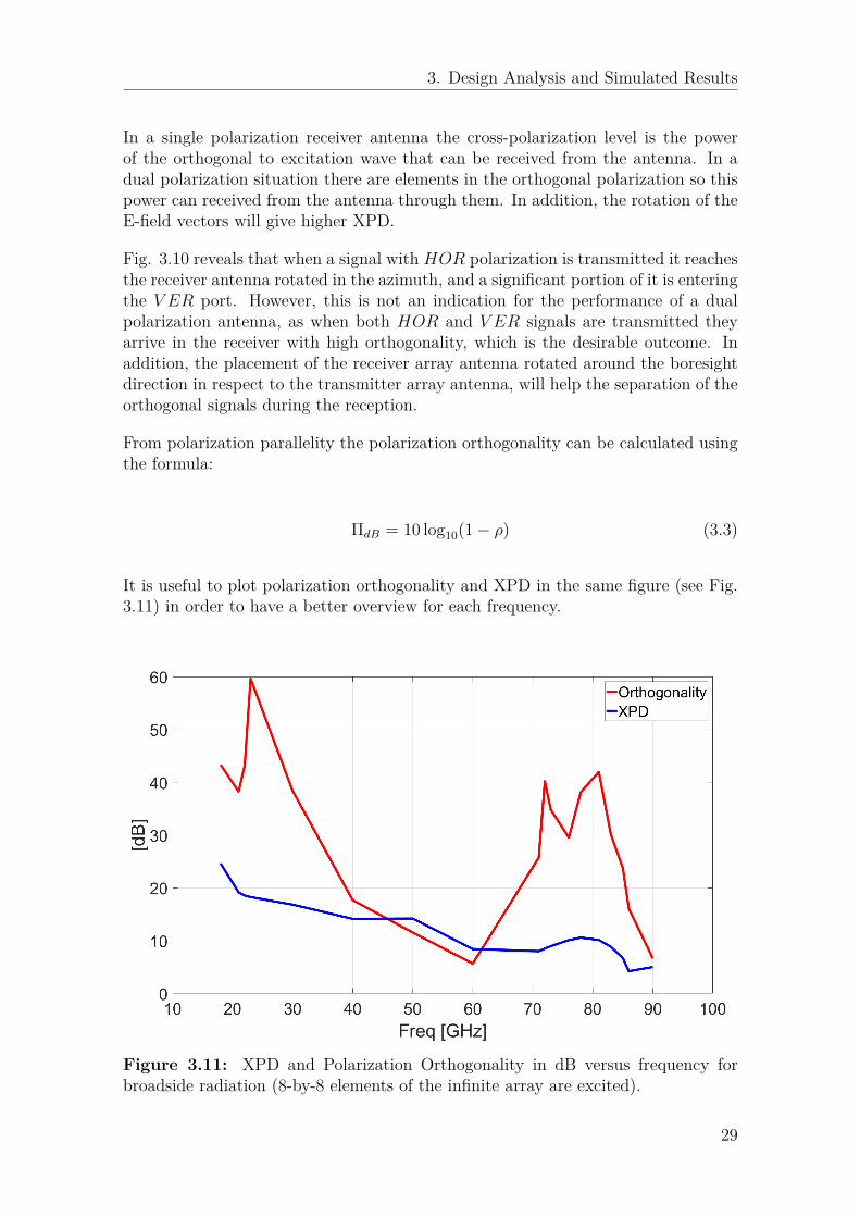
In a single polarization receiver antenna the cross-polarization level is the powerof the orthogonal to excitation wave that can be received from the antenna. In adual polarization situation there are elements in the orthogonal polarization so thispower can received from the antenna through them. In addition, the rotation of theE-field vectors will give higher XPD.
Fig. 3.10 reveals that when a signal with HOR polarization is transmitted it reachesthe receiver antenna rotated in the azimuth, and a significant portion of it is enteringthe V ER port. However, this is not an indication for the performance of a dualpolarization antenna, as when both HOR and V ER signals are transmitted theyarrive in the receiver with high orthogonality, which is the desirable outcome. Inaddition, the placement of the receiver array antenna rotated around the boresightdirection in respect to the transmitter array antenna, will help the separation of theorthogonal signals during the reception.
From polarization parallelity the polarization orthogonality can be calculated usingthe formula:
ΠdB = 10 log10(1− ρ) (3.3)
It is useful to plot polarization orthogonality and XPD in the same figure (see Fig.3.11) in order to have a better overview for each frequency.
Figure 3.11: XPD and Polarization Orthogonality in dB versus frequency forbroadside radiation (8-by-8 elements of the infinite array are excited).
29
3. Design Analysis and Simulated Results
3.2.3 Radiation Patterns
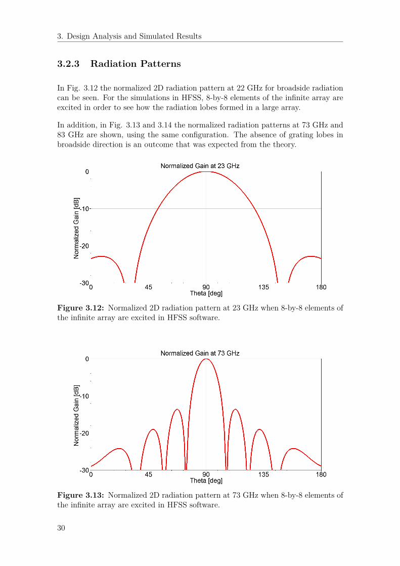
In Fig. 3.12 the normalized 2D radiation pattern at 22 GHz for broadside radiationcan be seen. For the simulations in HFSS, 8-by-8 elements of the infinite array areexcited in order to see how the radiation lobes formed in a large array.
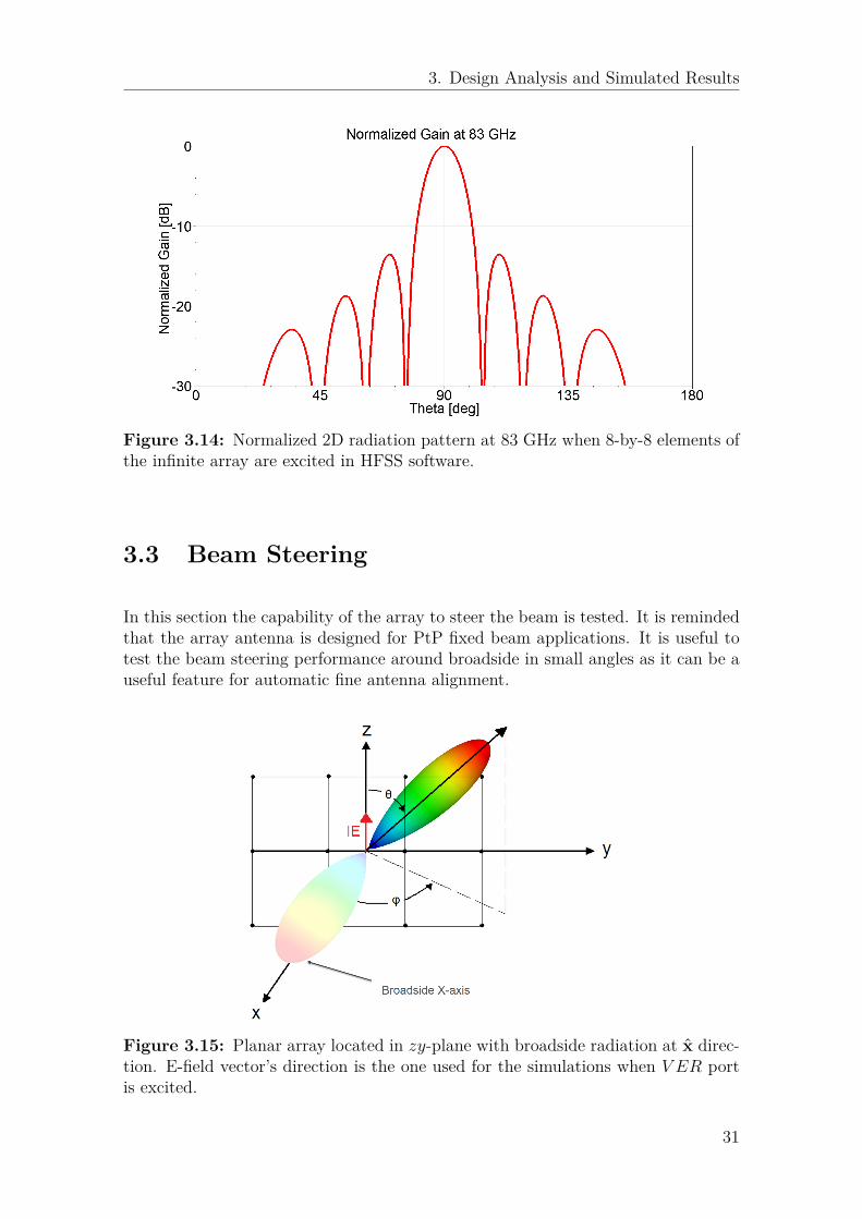
In addition, in Fig. 3.13 and 3.14 the normalized radiation patterns at 73 GHz and83 GHz are shown, using the same configuration. The absence of grating lobes inbroadside direction is an outcome that was expected from the theory.
Figure 3.12: Normalized 2D radiation pattern at 23 GHz when 8-by-8 elements ofthe infinite array are excited in HFSS software.
Figure 3.13: Normalized 2D radiation pattern at 73 GHz when 8-by-8 elements ofthe infinite array are excited in HFSS software.
30
3. Design Analysis and Simulated Results
Figure 3.14: Normalized 2D radiation pattern at 83 GHz when 8-by-8 elements ofthe infinite array are excited in HFSS software.
3.3 Beam Steering
In this section the capability of the array to steer the beam is tested. It is remindedthat the array antenna is designed for PtP fixed beam applications. It is useful totest the beam steering performance around broadside in small angles as it can be auseful feature for automatic fine antenna alignment.
Figure 3.15: Planar array located in zy-plane with broadside radiation at x direc-tion. E-field vector’s direction is the one used for the simulations when V ER portis excited.
31
3. Design Analysis and Simulated Results
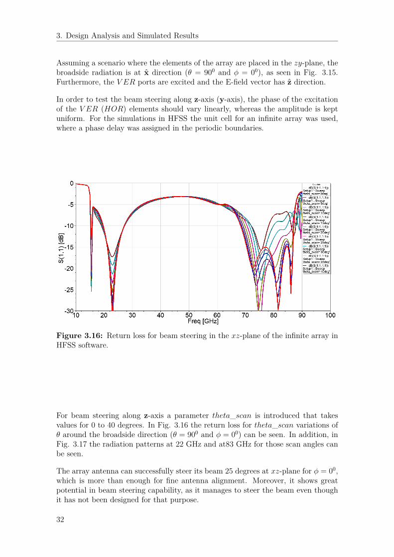
Assuming a scenario where the elements of the array are placed in the zy-plane, thebroadside radiation is at x direction (θ = 900 and φ = 00), as seen in Fig. 3.15.Furthermore, the V ER ports are excited and the E-field vector has z direction.
In order to test the beam steering along z-axis (y-axis), the phase of the excitationof the V ER (HOR) elements should vary linearly, whereas the amplitude is keptuniform. For the simulations in HFSS the unit cell for an infinite array was used,where a phase delay was assigned in the periodic boundaries.
Figure 3.16: Return loss for beam steering in the xz-plane of the infinite array inHFSS software.
For beam steering along z-axis a parameter theta_scan is introduced that takesvalues for 0 to 40 degrees. In Fig. 3.16 the return loss for theta_scan variations ofθ around the broadside direction (θ = 900 and φ = 00) can be seen. In addition, inFig. 3.17 the radiation patterns at 22 GHz and at83 GHz for those scan angles canbe seen.
The array antenna can successfully steer its beam 25 degrees at xz-plane for φ = 00,which is more than enough for fine antenna alignment. Moreover, it shows greatpotential in beam steering capability, as it manages to steer the beam even thoughit has not been designed for that purpose.
32
3. Design Analysis and Simulated Results
Figure 3.17: Realized gain at 22 GHz and 83 GHz for different beam θ angles andφ = 00 (in the xz-plane) when 8-by-8 elements of the infinite array are excited inHFSS software.
For beam steering along y-axis a parameter phi_scan is introduced that takes valuesfor 0 to 40 degrees. In Fig. 3.18 the return loss for phi_scan variations of φ aroundthe broadside direction (θ = 900 and φ = 00) can be seen. In addition, in Fig. 3.19the radiation patterns at 22 GHz and at83 GHz for those scan angles can be seen.
Figure 3.18: Return loss for beam steering in the xy-plane of the infinite array inHFSS software.
33

3. Design Analysis and Simulated Results
Figure 3.19: Realized gain at 22 GHz and 83 GHz for different beam φ angles andθ = 900 (in the xy-plane) when 8-by-8 elements of the infinite array are excited inHFSS software.
The array antenna can successfully steer its beam 15 degrees at xy-plane for θ = 900,which is enough for fine antenna alignment. We notice that the beam steeringperformance in this direction is not so good as at along z-axis for φ = 00.
3.4 Tolerance Analysis
In this section a tolerance analysis of the structure has been performed. The tol-erance analysis is performed using sensitivity analysis function of HFSS where pa-rameters vary and a specific performance parameter is measured. Then, from thatvariance a curve is created and depending its slope one can see how sensitive is thestructure performance to those variations.
Dimension tolerance analysis can be helpful during fabrication process in order toknow which parameters should be focus and avoid mistakes. In the following figuresthere are the results of the analysis for three different frequencies having return loss(reflection coefficient) as a performance parameter. Each parameter varies around20% around the optimal value.
3.4.1 Dimension Tolerance Analysis
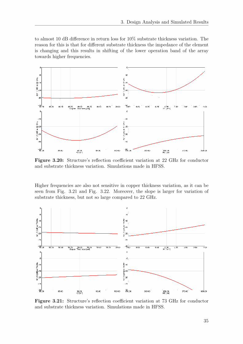
First, a tolerance analysis of the dimensions of the structure carried out. From Fig.3.20 it can be seen that the thickness of the copper does not affect the return lossat 22 GHz, whereas it is sensitive in variation of the substrate thickness, with 3 dB
34
3. Design Analysis and Simulated Results
to almost 10 dB difference in return loss for 10% substrate thickness variation. Thereason for this is that for different substrate thickness the impedance of the elementis changing and this results in shifting of the lower operation band of the arraytowards higher frequencies.
Figure 3.20: Structure’s reflection coefficient variation at 22 GHz for conductorand substrate thickness variation. Simulations made in HFSS.
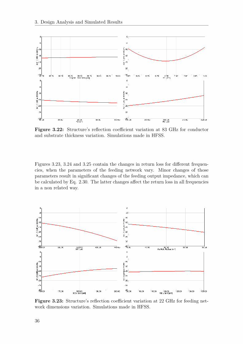
Higher frequencies are also not sensitive in copper thickness variation, as it can beseen from Fig. 3.21 and Fig. 3.22. Moreover, the slope is larger for variation ofsubstrate thickness, but not so large compared to 22 GHz.
Figure 3.21: Structure’s reflection coefficient variation at 73 GHz for conductorand substrate thickness variation. Simulations made in HFSS.
35
3. Design Analysis and Simulated Results
Figure 3.22: Structure’s reflection coefficient variation at 83 GHz for conductorand substrate thickness variation. Simulations made in HFSS.
Figures 3.23, 3.24 and 3.25 contain the changes in return loss for different frequen-cies, when the parameters of the feeding network vary. Minor changes of thoseparameters result in significant changes of the feeding output impedance, which canbe calculated by Eq. 2.30. The latter changes affect the return loss in all frequenciesin a non related way.
Figure 3.23: Structure’s reflection coefficient variation at 22 GHz for feeding net-work dimensions variation. Simulations made in HFSS.
36

3. Design Analysis and Simulated Results
Figure 3.24: Structure’s reflection coefficient variation at 73 GHz for feeding net-work dimension variation. Simulations made in HFSS.
Figure 3.25: Structure’s reflection coefficient variation at 83 GHz for feeding net-work dimensions variation. Simulations made in HFSS.
In figures 3.26, 3.27 and 3.28 the reflection coefficient variation due to the elementand the cap dimensions variations are shown.
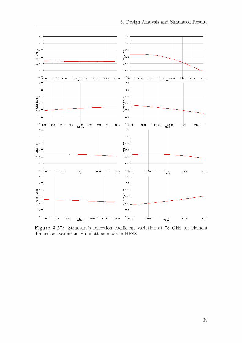
The most affected frequency is the 22 GHz, where both the size of the element andthe size of the caps shift the frequency. The second more sensitive frequency is the83 GHz as the 73 GHz seems to be affected only by the size of the cap on top ofthe element. As it has been mentioned earlier, E-band and 23 GHz band are atthe ”limit” of the frequency range that the tightly coupled capped bow-tie array
37

3. Design Analysis and Simulated Results
operates. As a result, the lower frequencies of the 23 GHz band and the higherfrequencies of the E-band are affected more by the variations of the dimensions ofthe structure.
Figure 3.26: Structure’s reflection coefficient variation at 22 GHz for element andcap dimensions variation. Simulations made in HFSS.
38
3. Design Analysis and Simulated Results
Figure 3.27: Structure’s reflection coefficient variation at 73 GHz for elementdimensions variation. Simulations made in HFSS.
39
3. Design Analysis and Simulated Results
Figure 3.28: Structure’s reflection coefficient variation at 83 GHz for elementdimensions variation. Simulations made in HFSS.
3.4.2 Material Tolerance Analysis
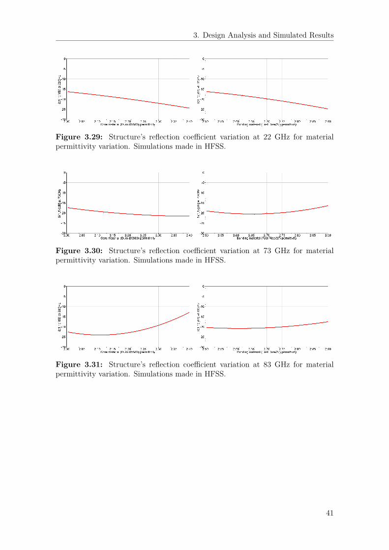
In this section the material tolerance analysis of the dielectric substrates carriedout. In Figures 3.29, 3.30 and 3.31 we can see the reflection coefficient variationwhen the core and the bonding material permittivity changes at 22 GHz, 73 GHzand 83 GHz respectively. The structure has high tolerance to 10% variation of thematerials permittivity, as the reflection coefficient divergence is less than 1.5 dB.
40
3. Design Analysis and Simulated Results
Figure 3.29: Structure’s reflection coefficient variation at 22 GHz for materialpermittivity variation. Simulations made in HFSS.
Figure 3.30: Structure’s reflection coefficient variation at 73 GHz for materialpermittivity variation. Simulations made in HFSS.
Figure 3.31: Structure’s reflection coefficient variation at 83 GHz for materialpermittivity variation. Simulations made in HFSS.
41

3. Design Analysis and Simulated Results
42
4Measurement and Fabrication
Considerations
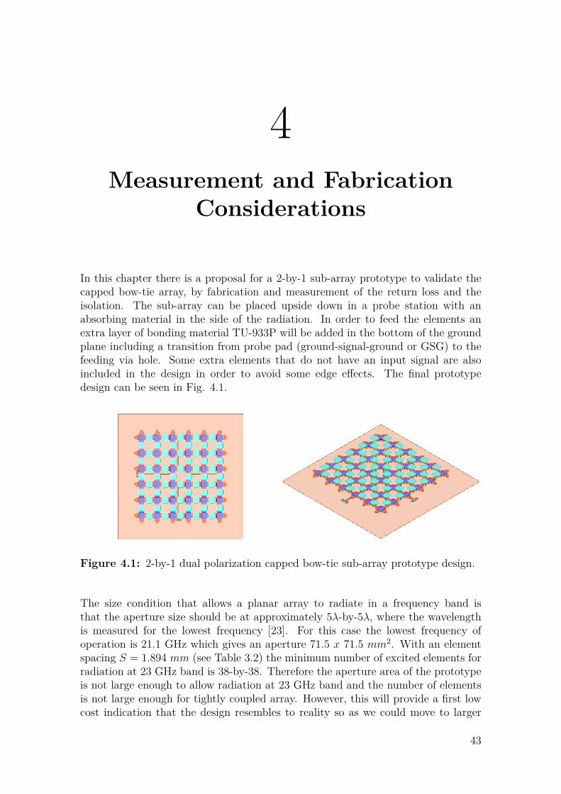
In this chapter there is a proposal for a 2-by-1 sub-array prototype to validate thecapped bow-tie array, by fabrication and measurement of the return loss and theisolation. The sub-array can be placed upside down in a probe station with anabsorbing material in the side of the radiation. In order to feed the elements anextra layer of bonding material TU-933P will be added in the bottom of the groundplane including a transition from probe pad (ground-signal-ground or GSG) to thefeeding via hole. Some extra elements that do not have an input signal are alsoincluded in the design in order to avoid some edge effects. The final prototypedesign can be seen in Fig. 4.1.
Figure 4.1: 2-by-1 dual polarization capped bow-tie sub-array prototype design.
The size condition that allows a planar array to radiate in a frequency band isthat the aperture size should be at approximately 5λ-by-5λ, where the wavelengthis measured for the lowest frequency [23]. For this case the lowest frequency ofoperation is 21.1 GHz which gives an aperture 71.5 x 71.5 mm2. With an elementspacing S = 1.894 mm (see Table 3.2) the minimum number of excited elements forradiation at 23 GHz band is 38-by-38. Therefore the aperture area of the prototypeis not large enough to allow radiation at 23 GHz band and the number of elementsis not large enough for tightly coupled array. However, this will provide a first lowcost indication that the design resembles to reality so as we could move to larger
43
4. Measurement and Fabrication Considerations
more costly arrays safely. The whole structure (the sub-array and the transition)will be simulated and the results will be compared to the measured ones. Goodresults are not expected, what matters is the resemblance between simulation andmeasurement.
Unfortunately, the fabrication procedure takes a lot of time and as a result thecomparison between simulation and measurement will not be included in this work,but in a future one.
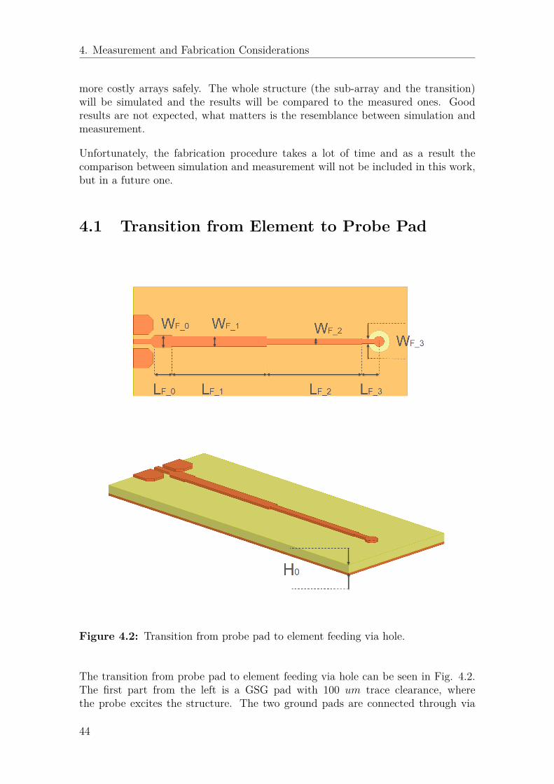
4.1 Transition from Element to Probe Pad
Figure 4.2: Transition from probe pad to element feeding via hole.
The transition from probe pad to element feeding via hole can be seen in Fig. 4.2.The first part from the left is a GSG pad with 100 um trace clearance, wherethe probe excites the structure. The two ground pads are connected through via
44
4. Measurement and Fabrication Considerations
holes with the ground plane of the sub-array. As a bonding material TU-933P isused with H0 = 120 um. A tapered transformer follows that is connected to a50 ohm transmission line. The probe will be calibrated to this point to have 50 ohmimpedance. After that there are two quarter wave transformers till a 77 ohm line,which is the input impedance of the balun transformer.
From microstrip transmission line theory [35] the widths of the lines are calculatedusing as:
W
H=
8eAe2A − 2 for W/H < 1
2π
[B − 1− ln(2B − 1) + εr − 1
2εr
(ln(B − 1) + 0.39− 0.61
εr
)]for W/H > 1
(4.1)
where
A = Z0
60
√εr + 1
2 + εr − 1εr + 1
(0.23 + 0.11
εr
)
B = 377π2Z0√εr
(4.2)
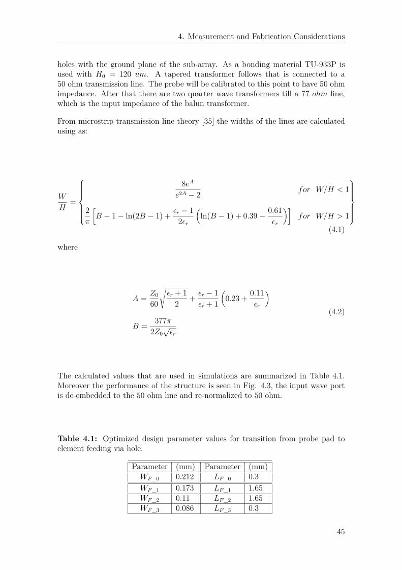
The calculated values that are used in simulations are summarized in Table 4.1.Moreover the performance of the structure is seen in Fig. 4.3, the input wave portis de-embedded to the 50 ohm line and re-normalized to 50 ohm.
Table 4.1: Optimized design parameter values for transition from probe pad toelement feeding via hole.
Parameter (mm) Parameter (mm)WF_0 0.212 LF_0 0.3WF_1 0.173 LF_1 1.65WF_2 0.11 LF_2 1.65WF_3 0.086 LF_3 0.3
45
4. Measurement and Fabrication Considerations
Figure 4.3: Transmission and reflection coefficients of the transition structure seenin Fig. 4.2.
4.2 Prototype Simulated Results
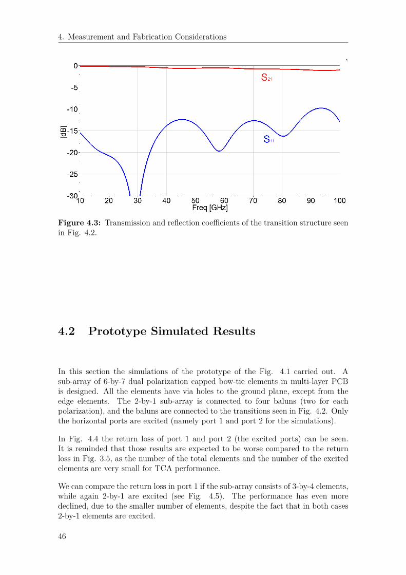
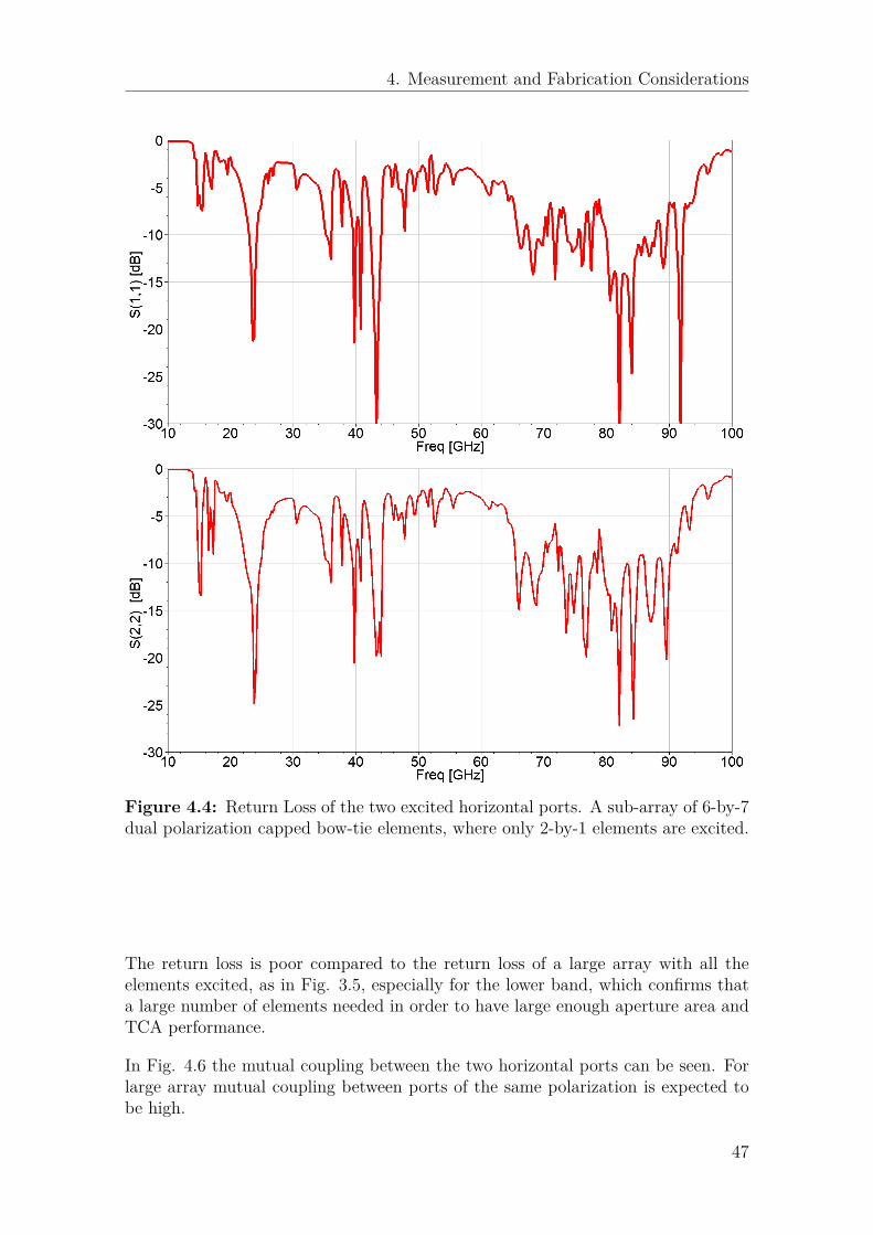
In this section the simulations of the prototype of the Fig. 4.1 carried out. Asub-array of 6-by-7 dual polarization capped bow-tie elements in multi-layer PCBis designed. All the elements have via holes to the ground plane, except from theedge elements. The 2-by-1 sub-array is connected to four baluns (two for eachpolarization), and the baluns are connected to the transitions seen in Fig. 4.2. Onlythe horizontal ports are excited (namely port 1 and port 2 for the simulations).
In Fig. 4.4 the return loss of port 1 and port 2 (the excited ports) can be seen.It is reminded that those results are expected to be worse compared to the returnloss in Fig. 3.5, as the number of the total elements and the number of the excitedelements are very small for TCA performance.
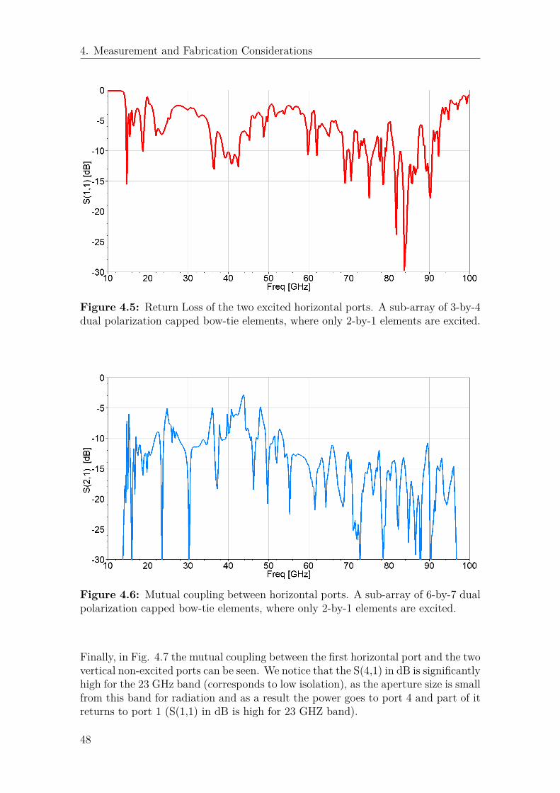
We can compare the return loss in port 1 if the sub-array consists of 3-by-4 elements,while again 2-by-1 are excited (see Fig. 4.5). The performance has even moredeclined, due to the smaller number of elements, despite the fact that in both cases2-by-1 elements are excited.
46
4. Measurement and Fabrication Considerations
Figure 4.4: Return Loss of the two excited horizontal ports. A sub-array of 6-by-7dual polarization capped bow-tie elements, where only 2-by-1 elements are excited.
The return loss is poor compared to the return loss of a large array with all theelements excited, as in Fig. 3.5, especially for the lower band, which confirms thata large number of elements needed in order to have large enough aperture area andTCA performance.
In Fig. 4.6 the mutual coupling between the two horizontal ports can be seen. Forlarge array mutual coupling between ports of the same polarization is expected tobe high.
47
4. Measurement and Fabrication Considerations
Figure 4.5: Return Loss of the two excited horizontal ports. A sub-array of 3-by-4dual polarization capped bow-tie elements, where only 2-by-1 elements are excited.
Figure 4.6: Mutual coupling between horizontal ports. A sub-array of 6-by-7 dualpolarization capped bow-tie elements, where only 2-by-1 elements are excited.
Finally, in Fig. 4.7 the mutual coupling between the first horizontal port and the twovertical non-excited ports can be seen. We notice that the S(4,1) in dB is significantlyhigh for the 23 GHz band (corresponds to low isolation), as the aperture size is smallfrom this band for radiation and as a result the power goes to port 4 and part of itreturns to port 1 (S(1,1) in dB is high for 23 GHZ band).
48
4. Measurement and Fabrication Considerations
Figure 4.7: Mutual coupling between the first horizontal port and the two verticalnon-excited ports. A sub-array of 6-by-7 dual polarization capped bow-tie elements,where only 2-by-1 elements are excited.
49

4. Measurement and Fabrication Considerations
50
5Conclusion
5.1 General Conclusions
In this work the design of a planar array in multi-layer PCB technology with cappedbow-tie dual polarization elements operating at E-band and at 23 GHz band ispresented. The simulations made with HFSS software, reveal that when the cappedbow-tie element is implemented as a large TCA can provide more than 15 dB returnloss at the two bands of interest, and at the same time keeps the orthogonalitybetween the two linear polarizations in a level the fulfills the specification (exceptof two single frequencies but with potential to fulfill as well). Moreover, the arrayis capable of steering its beam 25 degrees around broadside in the plane parallelto E-field and 15 degrees around broadside in the plane tangent to E-field, whichis satisfying for fine antenna alignment. On the other hand, the level of isolationbetween orthogonal ports should be higher. One, but still expensive solution is theuse of a shielded feeding network.
In terms of dimension tolerance, the performance of the design can be easily declinedand the lower operation band can be shifted, as more than 2 dB difference in returnloss is observed with 10% changes in element/feeding dimensions and substratethickness. The reason for that is the high dependence of the differential inputimpedance with the size of the element and the balun. On the other hand, thestructure has high tolerance in changes of the materials permittivity.
Furthermore, the design shows high scalability potential, the size of the element, thesize of the caps and the impedance provided by the feeding network can be tunedfor operation at different frequency bands. It must be noticed that the frequencyrange limit expressed in fractional bandwidth is 4.2:1, so the two operating bandsshould be inside this fractional bandwidth.
In order to achieve an array gain more than 38 dBi at E-band, which consists aspecification for PtP antennas, several thousands of elements are needed, and thecomplexity of the feeding network as well as the mechanics of the array will determinethe total manufacturing cost.
When compared to access point antennas in street level or in residential and public
51

5. Conclusion
areas this solution is more promising, as gain specification is more relaxed requiringless elements and less complex feeding structure. Furthermore, the operating fre-quencies are lower, so making elements and element spacing larger results in lowerfabrication cost and higher inter-port isolation (feeding via hole distance is larger).
In addition, a prototype is designed and simulated in order to be fabricated andmeasured. Simulations revealed that the performance in terms of return loss isdegraded compared to a large array, as the number of elements is not sufficient forTCA operation and radiation at 23 GHz band. However, the resemblance betweenthe simulations and the measurements can be a first indication to validate the designand proceed to larger arrays fabrication.
5.2 Future Work Proposal
This work only includes a proposal for a prototype and the validation of it requiresits fabrication and measurement. For this reason a future work that will focus onthe this matter should be done.
In addition, it would be interesting to test the dual polarization capped bow-tieTCA antenna design for access point array antennas and also test the beam steeringcapability.
Finally, a more detailed work for the feeding network that includes the total lossesshould be done. Different structures for differential feeding network should be inves-tigated, in order to improve the isolation between orthogonal ports and the losses.
52

Bibliography
[1] J. Yang, P.-S. Kildal, "FDTD design of a chinese hat feed for shallow mm-wavereflector antennas," IEEE AP-S International Symposium, Atlanta, June, 1998.
[2] M. Denstedt, T. Ostling, J. Yang, P.-S. Kildal, "Tripling bandwidth of hat feedby genetic algorithm optimization," IEEE AP-S 2007 in Hawaii, 10-15 June2007.
[3] W. Wei, J. Yang, T. Ostling, T. Schafer, "New hat feed for reflector antennasrealized without dielectrics for reducing manufacturing cost and improving re-flection coefficient," IET Microwaves Antennas & Propagation 5 (2011) 837-843.
[4] E. G. Geterud, J. Yang, T. Ostling, P. Bergmark, "Design and optimizationof compact wideband hat-fed reflector antenna for satellite communications,"IEEE Transactions on Antennas and Propagation 61, 125-133, 2013.
[5] E. G. Geterud, J. Yang, T. Ostling, "Wide band hat-fed reflector antenna forsatellite communications," in Proceedings of the 5th European Conference onAntennas and Propagation, EUCAP 2011. Rome, 11-15 April 2011, pp. 754-757.
[6] E. G. Geterud, J. Yang, T. Ostling, "Radome design for hat-fed reflector an-tenna," in Proceedings of 6th European Conference on Antennas and Propaga-tion, EuCAP 2012. Prague, 26-30 March 2012, pp. 2985-2988.
[7] J. Yang, A. Kishk, "A novel low-profile compact directional ultra-widebandantenna: the self-grounded bow-tie antenna," IEEE Transactions on Antennasand Propagation 60 (2012) 1214-1220.
[8] Y. Yu, J. Yang, T. McKelvey, B. Stoew, "Compact UWB indoor and through-wall radar with precise ranging and tracking,2 International Journal of Anten-nas and Propagation 2012 (2012) Article ID 678590.
[9] H. Raza, A. Hussain, J. Yang, P.-S. Kildal, "Wideband compact 4-port dualpolarized self-grounded bowtie antenna," IEEE Transactions on Antennas andPropagation 62 (2014) 4468-4473.
[10] J. Yang, A. Kishk, "The self-grounded bow-tie antenna," in 2011 IEEE Inter-national Symposium on Antennas and Propagation, Spokane, USA, 3-8 July,
53

Bibliography
2011, 2011, pp. 1452-1455.
[11] S. Abtahi, J. Yang, S. Kidborg, "A new compact multiband antenna for strokediagnosis system over 0.5-3 GHz," Microwave and Optical Technology Letters54 (2012), 2342-2346.
[12] Jian Yang, Jonas Flygare, B. Billade, "Development of quadruple-ridge flaredhorn with spline-defined profile for band b of the wide band single pixel feed(WBSPF) advanced instrumentation programme for SKA," in 2016 IEEE AP-SInternational Symposium, Puerto Rico, June 25-July 1, 2016, 2016.
[13] B. Munk et al., “A Low-Profile Broadband Phased Array Antenna,” Antennasand Propagation Society International Symposium, 2003. IEEE , vol.2, no., pp.448- 451 vol.2, 22-27, June 2003.
[14] Justin A. Kasemodel, Chi-Chih Chen, and John L. Volakis, “A MiniaturizationTechnique for Wideband Tightly Coupled Phased Arrays,” Antennas and Prop-agation Society International Symposium, 2009. APSURSI ’09. IEEE , vol., no.,pp.1-4, 1-5, June 2009.
[15] Chin-Shen Lin et al., “Analysis of Multiconductor Coupled-Line MarchandBaluns for Miniature MMIC Design,” IEEE Transactions On Microwave TheoryAnd Techniques, vol. 55, no. 6, June 2007.
[16] Steven S. Holland, and Marinos N. Vouvakis, “The Planar Ultrawideband Mod-ular Antenna (PUMA),” IEEE Transactions on Antennas and Propagation, vol.60, no. 1, January 2012.
[17] Markus H. Novak, Felix A. Miranday, and John L. Volakis, “An Ultra-Wideband Millimeter-Wave Phased Array,” in European Conference on An-tennas and Propagation (EuCAP), 2016 .
[18] Markus H. Novak, Felix A. Miranday, and John L. Volakis, “Low Cost Ultra-Wideband Millimeter-Wave Array,” IEEE International Symposium on Anten-nas and Propagation (APSURSI), 2016 .
[19] William F. Moulder, Kubilay Sertel, and John L. Volakis, “UltrawidebandSuperstrate-Enhanced Substrate-Loaded Array With Integrated Feed,” IEEETransactions on Antennas and Propagation, vol. 61, no. 1, November 2013.
[20] William F. Moulder, Kubilay Sertel, and John L. Volakis, “Superstrate-Enhanced Ultrawideband Tightly Coupled Array With Resistive FSS,” IEEETransactions on Antennas and Propagation, vol. 60, no. 9, September 2013.
[21] Mark Jones, and James Rawnick, “A New Approach to Broadband Array De-sign Using Tightly Coupled Elements,” Harris Corporation, Melbourne, FL,2007.
54

Bibliography
[22] D. Bartholomew, “Optimum design for a broadband microstrip balun,” Elec-tronics Letters, vol. 13, no. 17, pp. 510–511, August 1977.
[23] Henrik Holter and Hans Steyskal, “Some Experiences From FDTD Analysisof Infinite and Finite Multi-Octave Phased Arrays,” IEEE Transactions onAntennas and Propagation, vol. 50, no. 12, December 2002.
[24] Timothy E. Durham et al., “Design of an 8-40 GHz Antenna for the WidebandInstrument for Snow Measurements,” IEEE International Symposium on An-tennas and Propagation & USNC/URSI National Radio Science Meeting, July2015.
[25] D. S. Filipovic et al., “Modeling, Design, Fabrication, and Performance ofRectangular µ-Coaxial Lines and Components,” IEEE MTT-S InternationalMicrowave Symposium Digest, June 2006.
[26] William F. Moulder, “Novel Implementations of Ultrawideband Tightly Cou-pled Antenna Arrays,” Ph.D dissertation, The Ohio State University, 2012.
[27] Justin A. Kasemodel, “Realization of a Planar Low-Profile Broadband PhasedArray Antenna,” Presented in Partial Fulfillment of the Requirements for theDegree Doctor of Philosophy, The Ohio State University, 2010.
[28] Nathanael J. Smith, “Development of a 1800 Hybrid Balun to Feed a TightlyCoupled Dipole X-Band Array,” Senior Honors Thesis, The Ohio State Univer-sity, 2010.
[29] Kalyany Vinayagamoorthy, “Design and Implementation of Wideband Balunsfor Archimedean Spiral Antennas,” Master’s Thesis, Queensland University ofTechnology, August 2011.
[30] Jonas Edstam, “Microwave Backhaul Gets a Boost with Multiband,” EricssonTechnology Review, Charting the Future of Innovation, vol. 93, January 2016.
[31] John L. Volakis, “Ultra Wideband Phased Arrays and Transceivers,” IEEEInternational Symposium on Antennas and Propagation, Workshop 5, October2006.
[32] Mikael Coldrey et al., “Wireless Backhaul in Future Heterogeneous Networks,”Ericsson Review, pp. 28-36, February 2014.
[33] Kildal, Per-Simon. Foundations of Antenna Engineering: A Unified Approachfor Line-of-Sight and Multipath. Gothenburg: Kildal Antenna AB, 2015. Print.
[34] Mailloux, Robert J.. Phased Array Antenna Handbook. Boston: Artech house,Inc, 1994. Print.
[35] Pozar, David M.. Microwave Engineering, 4th Edition. Massachusetts: JohnWiley & Sons, Inc, 2012. Print.
55

Bibliography
[36] ETSI GS mWT (V1.1.1): “millimetre Wave Transmission (mWT); Analysis ofantennas for millimetre wave transmission”.
[37] ETSI EN 300 833 (V1.4.1): “Fixed Radio Systems; Point-to-point antennas;Antennas for point-to-point fixed radio systems; Antennas for point-to-pointfixed radio systems operating in the frequency band 3 GHz to 60 GHz”.
[38] ETSI EN 302 2177-4-2 (V1.5.1): “Fixed Radio Systems; Characteristics andrequirements for point-to-point equipment and antennas; Part 4-2: Antennas;Harmonized EN covering the essential requirements of article 3.2 of the R&TTEDirective”.
56