DLPS057C –NOVEMBER 2014–REVISED …€¢ Screenless Display/Portable Home Cinema • Mobile...
62
Product Folder Order Now Technical Documents Tools & Software Support & Community An IMPORTANT NOTICE at the end of this data sheet addresses availability, warranty, changes, use in safety-critical applications, intellectual property matters and other important disclaimers. PRODUCTION DATA. DLPC3439 DLPS057C – NOVEMBER 2014 – REVISED SEPTEMBER 2017 DLPC3439 Display Controller 1 1 Features 1• Display Controller for DLP4710 (.47 1080p) TRP DMD – Dedicated 2xDLPC3439 Controller to Drive DLP4710 DMD – Supports Input Image Sizes up to 1080p – Low-Power DMD Interface with Interface Training • 24-Bit, Input Pixel Interface Support: – Parallel Interface – Pixel Clock up to 150 MHz – Multiple Input Pixel Data Format Options • Pixel Data Processing: – IntelliBright™ Suite of Image Processing Algorithms – Content Adaptive Illumination Control – Local Area Brightness Boost – Image Resizing (Scaling) – Color Coordinate Adjustment – Programmable Degamma – Active Power Management Processing – Color Space Conversion – 4:2:2 to 4:4:4 Chroma Interpolation • Package: – 201-Pin, 13-mm × 13-mm, 0.8-mm Pitch, NFBGA • External Flash Support • Compatible with the DLPA3000 and DLPA3005 PMIC/LED Drivers • Auto DMD Parking at Power Down • Embedded Frame Memory (eDRAM) • System Features: – I 2 C Control of Device Configuration – Programmable Splash Screens – Programmable LED Current Control – One Frame Latency 2 Applications • Mobile Accessory Full HD Projector • Battery Powered Smart Full HD Projector • Screenless Display/Portable Home Cinema • Mobile Professional Projector • Interactive Display • Low-Latency Gaming Display • Wearable Display (Near Eye or Head Mounted) • Digital Signage 3 Description The 2x DLPC3439 digital controller, part of the DLP4710 (.47 1080p) chipset, supports reliable operation of the DLP4710 digital micromirror device (DMD). The DLPC3439 controller provides a convenient, multi-functional interface between system electronics and the DMD, enabling small form factor, low power, and high resolution full HD displays. Device Information (1) PART NUMBER PACKAGE BODY SIZE (NOM) DLPC3439 NFBGA (201) 13.00 × 13.00 mm 2 (1) For all available packages, see the orderable addendum at the end of the data sheet. Simplified Schematic
Transcript of DLPS057C –NOVEMBER 2014–REVISED …€¢ Screenless Display/Portable Home Cinema • Mobile...

Product
Folder
Order
Now
Technical
Documents
Tools &
Software
Support &Community
An IMPORTANT NOTICE at the end of this data sheet addresses availability, warranty, changes, use in safety-critical applications,intellectual property matters and other important disclaimers. PRODUCTION DATA.
DLPC3439DLPS057C –NOVEMBER 2014–REVISED SEPTEMBER 2017
DLPC3439 Display Controller
1
1 Features1• Display Controller for DLP4710 (.47 1080p) TRP
DMD– Dedicated 2xDLPC3439 Controller to Drive
DLP4710 DMD– Supports Input Image Sizes up to 1080p– Low-Power DMD Interface with Interface
Training• 24-Bit, Input Pixel Interface Support:
– Parallel Interface– Pixel Clock up to 150 MHz– Multiple Input Pixel Data Format Options
• Pixel Data Processing:– IntelliBright™ Suite of Image Processing
Algorithms– Content Adaptive Illumination Control– Local Area Brightness Boost
– Image Resizing (Scaling)– Color Coordinate Adjustment– Programmable Degamma– Active Power Management Processing– Color Space Conversion– 4:2:2 to 4:4:4 Chroma Interpolation
• Package:– 201-Pin, 13-mm × 13-mm, 0.8-mm Pitch,
NFBGA• External Flash Support• Compatible with the DLPA3000 and DLPA3005
PMIC/LED Drivers• Auto DMD Parking at Power Down• Embedded Frame Memory (eDRAM)• System Features:
– I2C Control of Device Configuration– Programmable Splash Screens– Programmable LED Current Control– One Frame Latency
2 Applications• Mobile Accessory Full HD Projector• Battery Powered Smart Full HD Projector• Screenless Display/Portable Home Cinema• Mobile Professional Projector• Interactive Display• Low-Latency Gaming Display• Wearable Display (Near Eye or Head Mounted)• Digital Signage
3 DescriptionThe 2x DLPC3439 digital controller, part of theDLP4710 (.47 1080p) chipset, supports reliableoperation of the DLP4710 digital micromirror device(DMD). The DLPC3439 controller provides aconvenient, multi-functional interface between systemelectronics and the DMD, enabling small form factor,low power, and high resolution full HD displays.
Device Information(1)
PART NUMBER PACKAGE BODY SIZE (NOM)DLPC3439 NFBGA (201) 13.00 × 13.00 mm2
(1) For all available packages, see the orderable addendum atthe end of the data sheet.
Simplified Schematic

2
DLPC3439DLPS057C –NOVEMBER 2014–REVISED SEPTEMBER 2017 www.ti.com
Product Folder Links: DLPC3439
Submit Documentation Feedback Copyright © 2014–2017, Texas Instruments Incorporated
Table of Contents1 Features .................................................................. 12 Applications ........................................................... 13 Description ............................................................. 14 Revision History..................................................... 35 Pin Configuration and Functions ......................... 46 Specifications....................................................... 15
6.1 Absolute Maximum Ratings .................................... 156.2 ESD Ratings............................................................ 156.3 Recommended Operating Conditions..................... 166.4 Thermal Information ................................................ 166.5 Electrical Characteristics over Recommended
Operating Conditions .............................................. 176.6 Electrical Characteristics......................................... 186.7 High-Speed Sub-LVDS Electrical Characteristics... 206.8 Low-Speed SDR Electrical Characteristics............. 216.9 System Oscillators Timing Requirements ............... 226.10 Power-Up and Reset Timing Requirements ......... 226.11 Parallel Interface Frame Timing Requirements .... 236.12 Parallel Interface General Timing Requirements .. 246.13 Flash Interface Timing Requirements ................... 25
7 Parameter Measurement Information ................ 297.1 HOST_IRQ Usage Model ....................................... 297.2 Input Source ........................................................... 30
8 Detailed Description ............................................ 328.1 Overview ................................................................. 328.2 Functional Block Diagram ....................................... 32
8.3 Feature Description................................................. 328.4 Device Functional Modes........................................ 41
9 Application and Implementation ........................ 429.1 Application Information............................................ 429.2 Typical Application ................................................. 43
10 Power Supply Recommendations ..................... 4510.1 DLPC3439 System Design Consideration ............ 4510.2 System Power-Up and Power-Down Sequence ... 4510.3 DLPC3439 Power-Up Initialization Sequence ...... 4710.4 DMD Fast PARK Control (PARKZ)....................... 4810.5 Hot Plug Usage..................................................... 4810.6 Maximum Signal Transition Time.......................... 48
11 Layout................................................................... 4911.1 Layout Guidelines ................................................. 4911.2 Layout Example .................................................... 5311.3 Thermal Considerations ........................................ 53
12 Device and Documentation Support ................. 5512.1 Device Support .................................................... 5512.2 Related Links ........................................................ 5712.3 Community Resources.......................................... 5712.4 Trademarks ........................................................... 5712.5 Electrostatic Discharge Caution............................ 5712.6 Glossary ................................................................ 57
13 Mechanical, Packaging, and OrderableInformation ........................................................... 5713.1 Package Option Addendum .................................. 58

3
DLPC3439www.ti.com DLPS057C –NOVEMBER 2014–REVISED SEPTEMBER 2017
Product Folder Links: DLPC3439
Submit Documentation FeedbackCopyright © 2014–2017, Texas Instruments Incorporated
4 Revision HistoryNOTE: Page numbers for previous revisions may differ from page numbers in the current version.
Changes from Revision B (January 2016) to Revision C Page
• Updated V(VCC18) maximum from 18 mA to 62 mA in Electrical Characteristics over Recommended OperatingConditions ............................................................................................................................................................................ 17
• Updated V(VCC18) + V(VCC_INTF) + V(VCC_FLSH) maximum from 22.5 mA to 66.5 mA in Electrical Characteristics overRecommended Operating Conditions ................................................................................................................................. 17
• Removed "and 3D Display Orientation" in title of Input Source - Frame Rates .................................................................. 30• Modified description in Overview to account for two DLPC3439 controllers........................................................................ 32• Included additional DLPC3439 compatible SPI flash device options in Table 6.................................................................. 35• Updated Device Markings image, changed manufacturing site to generic code ................................................................. 55• In Device Markings note, updated link for DLPC3439 resolutions on the DMD supported per part number to refer to
Input Source - Frame Rates ................................................................................................................................................ 56• Added DLPA3000 to Table 13.............................................................................................................................................. 57• Added MSL Peak Temp to Packaging Information .............................................................................................................. 58
Changes from Revision A (June 2015) to Revision B Page
• Corrected device markings .................................................................................................................................................. 55• Updated Device Markings image and table ......................................................................................................................... 55
Changes from Original (February 2014) to Revision A Page
• Changed device status from Product Preview to Production Data and released full version of the document. .................... 1

4
DLPC3439DLPS057C –NOVEMBER 2014–REVISED SEPTEMBER 2017 www.ti.com
Product Folder Links: DLPC3439
Submit Documentation Feedback Copyright © 2014–2017, Texas Instruments Incorporated
5 Pin Configuration and Functions
ZEZ Package201-Pin NFBGA
Bottom View
1 2 3 4 5 6 7 8 9 10 11 12 13 14 15
ADMD_LS_C
LK
DMD_LS_W
DATA
DMD_HS_W
DATAH_P
DMD_HS_W
DATAG_P
DMD_HS_W
DATAF_P
DMD_HS_W
DATAE_P
DMD_HS_CLK_
P
DMD_HS_W
DATAD_P
DMD_HS_W
DATAC_P
DMD_HS_W
DATAB_P
DMD_HS_W
DATAA_PCMP_OUT SPI0_CLK SPI0_CSZ0 CMP_PWM
BDMD_DEN_
ARSTZ
DMD_LS_R
DATA
DMD_HS_W
DATAH_N
DMD_HS_W
DATAG_N
DMD_HS_W
DATAF_N
DMD_HS_W
DATAE_N
DMD_HS_CLK_
N
DMD_HS_W
DATAD_N
DMD_HS_W
DATAC_N
DMD_HS_W
DATAB_N
DMD_HS_W
DATAA_NSPI0_DIN SPI0_DOUT LED_SEL_1 LED_SEL_0
C DD3P DD3N VDDLP12 VSS VDD VSS VCC VSS VCCHWTEST_E
NRESETZ SPI0_CSZ1 PARKZ GPIO_00 GPIO_01
D DD2P DD2N VDD VCC VDD VSS VDD VSS VDD VSS VCC_FLSH VDD VDD GPIO_02 GPIO_03
E DCLKP DCLKN VDD VSS VCC VSS GPIO_04 GPIO_05
F DD1P DD1N RREF VSS VSS VSS VSS VSS VSS VCC VDD GPIO_06 GPIO_07
G DD0P DD0N VSS_PLLM VSS VSS VSS VSS VSS VSS VSS VSS GPIO_08 GPIO_09
HPLL_REFCL
K_IVDD_PLLM VSS_PLLD VSS VSS VSS VSS VSS VSS VSS VDD GPIO_10 GPIO_11
JPLL_REFCL
K_OVDD_PLLD VSS VDD VSS VSS VSS VSS VSS VDD VSS GPIO_12 GPIO_13
K PDATA_1 PDATA_0 VDD VSS VSS VSS VSS VSS VSS VSS VCC GPIO_14 GPIO_15
L PDATA_3 PDATA_2 VSS VDD VDD VDD GPIO_16 GPIO_17
M PDATA_5 PDATA_4 VCC_INTF VSS VSS VDD VCC_INTF VSS VDD VDD VCC VSS JTAGTMS1 GPIO_18 GPIO_19
N PDATA_7 PDATA_6 VCC_INTFPDM_CVS_
TEHSYNC_CS 3DR VCC_INTF HOST_IRQ IIC0_SDA IIC0_SCL JTAGTMS2 JTAGTDO2 JTAGTDO1 TSTPT_6 TSTPT_7
P VSYNC_WEDATEN_CM
DPCLK PDATA_11 PDATA_13 PDATA_15 PDATA_17 PDATA_19 PDATA_21 PDATA_23 JTAGTRSTZ JTAGTCK JTAGTDI TSTPT_4 TSTPT_5
R PDATA_8 PDATA_9 PDATA_10 PDATA_12 PDATA_14 PDATA_16 PDATA_18 PDATA_20 PDATA_22 IIC1_SDA IIC1_SCL TSTPT_0 TSTPT_1 TSTPT_2 TSTPT_3
DLPC3439www.ti.com DLPS057C –NOVEMBER 2014–REVISED SEPTEMBER 2017
5
Product Folder Links: DLPC3439
Submit Documentation FeedbackCopyright © 2014–2017, Texas Instruments Incorporated
Figure 1. 13 mm × 13 mm Package – VF Ball Grid Array

6
DLPC3439DLPS057C –NOVEMBER 2014–REVISED SEPTEMBER 2017 www.ti.com
Product Folder Links: DLPC3439
Submit Documentation Feedback Copyright © 2014–2017, Texas Instruments Incorporated
(1) If operation does not call for an external pullup and there is no external logic that might overcome the weak internal pulldown resistor,then this I/O can be left open or unconnected for normal operation. If operation does not call for an external pullup, but there is externallogic that might overcome the weak internal pulldown resistor, then an external pulldown resistor is recommended to ensure a logic low.
(2) External pullup resistor must be 8 kΩ, or less, for pins with internal pullup or down resistors.(3) If operation does not call for an external pullup and there is no external logic that might overcome the weak internal pulldown resistor,
then the TSTPT I/O can be left open/unconnected for normal operation. If operation does not call for an external pullup but there isexternal logic that might overcome the weak internal pulldown resistor, then an external pulldown resistor is recommended to ensure alogic low.
Pin Functions – Board Level Test, Debug, and InitializationPIN
I/O DESCRIPTIONNAME NUMBER
HWTEST_EN C10 I6Manufacturing test enable signal. This signal should be connected directly to ground on thePCB for normal operation.
PARKZ C13 I6
DMD fast PARK control (active low Input, hysteresis buffer). PARKZ must be set high to enablenormal operation. PARKZ should be set high prior to releasing RESETZ (that is, prior to thelow-to-high transition on the RESETZ input). PARKZ should be set low for a minimum of 32 µsbefore any power is removed from the DLPC3439 such that the fast DMD PARK operation canbe completed. Note for PARKZ, fast PARK control should only be used when loss of power iseminent and beyond the control of the host processor (for example, when the external powersource has been disconnected or the battery has dropped below a minimum level). The longestlifetime of the DMD may not be achieved with the fast PARK operation. The longest lifetime isachieved with a normal PARK operation. Because of this, PARKZ is typically used inconjunction with a normal PARK request control input through GPIO_08. The difference beingthat when the host sets PROJ_ON low, which connects to both GPIO_08 and the DLPA3000 orDLPA3005 PMIC chip, the DLPC3439 takes much longer than 32 µs to park the mirrors. TheDLPA3000/DLPA3005 holds on all power supplies, and keep RESETZ high, until the longermirror parking has completed. This longer mirror parking time, of up to 500 µs, ensures thelongest DMD lifetime and reliability.The DLPA3000/DLPA3005 monitors power to the DLPC3439 and detects an eminent powerloss condition and drives the PARKZ signal accordingly.
Reserved P12 I6 TI internal use. Should be left unconnected.Reserved P13 I6 TI internal use. Should be left unconnected.Reserved N13 (1) O1 TI internal use. Should be left unconnected.Reserved N12 (1) O1 TI internal use. Should be left unconnected.Reserved M13 I6 TI internal use. Should be left unconnected.Reserved N11 I6 TI internal use. Should be left unconnected.
Reserved P11 I6TI internal useThis pin must be tied to ground, through an external 8-kΩ, or less, resistor for normal operation.Failure to tie this pin low during normal operation will cause startup and initialization problems.
RESETZ C11 I6
DLPC3439 power-on reset (active low input, hysteresis buffer). Self-configuration starts when alow-to-high transition is detected on RESETZ. All ASIC power and clocks must be stable beforethis reset is de-asserted. Note that the following signals will be tri-stated while RESETZ isasserted:• SPI0_CLK, SPI0_DOUT, SPI0_CSZ0• SPI0_CSZ1, and GPIO(19:00)External pullups or downs (as appropriate) should be added to all tri-stated output signals listed(including bidirectional signals to be configured as outputs) to avoid floating ASIC outputsduring reset if connected to devices on the PCB that can malfunction. For SPI, at a minimum,any chip selects connected to the devices should have a pullup.Unused bidirectional signals can be functionally configured as outputs to avoid floating ASICinputs after RESETZ is set high.The following signals are forced to a logic low state while RESETZ is asserted andcorresponding I/O power is applied:• LED_SEL_0, LED_SEL_1 and DMD_DEN_ARSTZNo signals will be in their active state while RESETZ is asserted.Note that no I2C activity is permitted for a minimum of 500 ms after RESETZ (and PARKZ) areset high.
TSTPT_0 R12 B1
Test pin 0 (includes weak internal pulldown) – tri-stated while RESETZ is asserted low.Sampled as an input test mode selection control approximately 1.5 µs after de-assertion ofRESETZ, and then driven as an output.Normal use: Reserved for test output. Should be left open or unconnected for normal use.Note: An external pullup should not be applied to this pin to avoid putting the DLPC3439 in atest mode.Without external pullup (2)
Feeds TMSEL(0)With external pullup (3)
Feeds TMSEL(0)
7
DLPC3439www.ti.com DLPS057C –NOVEMBER 2014–REVISED SEPTEMBER 2017
Product Folder Links: DLPC3439
Submit Documentation FeedbackCopyright © 2014–2017, Texas Instruments Incorporated
Pin Functions – Board Level Test, Debug, and Initialization (continued)PIN
I/O DESCRIPTIONNAME NUMBER
TSTPT_1 R13 B1
Test pin 1 (includes weak internal pulldown) – tri-stated while RESETZ is asserted low.Sampled as an input test mode selection control approximately 1.5 µs after de-assertion ofRESETZ and then driven as an output.Normal use: Reserved for test output. Should be left open or unconnected for normal use.Note: An external pullup should not be applied to this pin to avoid putting the DLPC3439 in atest mode.Without external pullup (2)
Feeds TMSEL(1)With external pullup (3)
Feeds TMSEL(1)
TSTPT_2 R14 B1
Test pin 2 (includes weak internal pulldown) – tri-stated while RESETZ is asserted low.Sampled as an input test mode selection control approximately 1.5 µs after de-assertion ofRESETZ and then driven as an output.Normal use: Reserved for test output. Should be left open or unconnected for normal use.Note: An external pullup should not be applied to this pin to avoid putting the DLPC3439 in atest mode.Without external pullup (2)
Feeds TMSEL(2)With external pullup (3)
Feeds TMSEL(2)
TSTPT_3 R15 B1
Test pin 3 (includes weak internal pulldown) – tri-stated while RESETZ is asserted low.Sampled as an input test mode selection control approximately 1.5 µs after de-assertion ofRESETZ and then driven as an output.Normal use: Reserved for test output. Should be left open or unconnected for normal use.
TSTPT_4 P14 B1
Test pin 4 (includes weak internal pulldown) – tri-stated while RESETZ is asserted low.Sampled as an input test mode selection control approximately 1.5 µs after de-assertion ofRESETZ and then driven as an output.Normal use: Reserved for test output. Should be left open or unconnected for normal use.
TSTPT_5 P15 B1
Test pin 5 (includes weak internal pulldown) – tri-stated while RESETZ is asserted low.Sampled as an input test mode selection control approximately 1.5 µs after de-assertion ofRESETZ and then driven as an output.Normal use: Reserved for test output. Should be left open or unconnected for normal use.
TSTPT_6 N14 B1
Test pin 6 (includes weak internal pulldown) – tri-stated while RESETZ is asserted low.Sampled as an input test mode selection control approximately 1.5 µs after de-assertion ofRESETZ and then driven as an output.Normal use: Reserved for test output. Should be left open or unconnected for normal use.Alternative use: None. External logic shall not unintentionally pull this pin high to avoid puttingthe DLPC3439 in a test mode.
TSTPT_7 N15 B1
Test pin 7 (includes weak internal pulldown) – tri-stated while RESETZ is asserted low.Sampled as an input test mode selection control approximately 1.5 µs after de-assertion ofRESETZ and then driven as an output.Normal use: Reserved for test output. Should be left open or unconnected for normal use.

8
DLPC3439DLPS057C –NOVEMBER 2014–REVISED SEPTEMBER 2017 www.ti.com
Product Folder Links: DLPC3439
Submit Documentation Feedback Copyright © 2014–2017, Texas Instruments Incorporated
(1) PDATA(23:0) bus mapping is pixel format and source mode dependent. See later sections for details.(2) PDM_CVS_TE is optional for parallel interface operation. If unused, inputs should be grounded or pulled down to ground through an
external resistor (8 kΩ or less).(3) Pixel clock capture edge is software programmable.(4) The parallel data mask signal input is optional for parallel interface operations. If unused, inputs should be grounded or pulled down to
ground through an external resistor (8 kΩ or less).(5) VSYNC, HSYNC, and DATAEN polarity is software programmable.
Pin Functions – Parallel Port Input Data and Control (1) (2)
PINI/O
DESCRIPTIONNAME NUMBER PARALLEL RGB MODE
PCLK P3 I11 Pixel clock (3)
PDM_CVS_TE N4 B5 Parallel data mask (4)
VSYNC_WE P1 I11 Vsync (5)
HSYNC_CS N5 I11 Hsync (5)
DATAEN_CMD P2 I11 Data Valid (5)
(TYPICAL RGB 888)PDATA_0PDATA_1PDATA_2PDATA_3PDATA_4PDATA_5PDATA_6PDATA_7
K2K1L2L1M2M1N2N1
I11
Blue (bit weight 1)Blue (bit weight 2)Blue (bit weight 4)Blue (bit weight 8)Blue (bit weight 16)Blue (bit weight 32)Blue (bit weight 64)Blue (bit weight 128)(TYPICAL RGB 888)
PDATA_8PDATA_9PDATA_10PDATA_11PDATA_12PDATA_13PDATA_14PDATA_15
R1R2R3P4R4P5R5P6
I11
Green (bit weight 1)Green (bit weight 2)Green (bit weight 4)Green (bit weight 8)Green (bit weight 16)Green (bit weight 32)Green (bit weight 64)Green (bit weight 128)(TYPICAL RGB 888)
PDATA_16PDATA_17PDATA_18PDATA_19PDATA_20PDATA_21PDATA_22PDATA_23
R6P7R7P8R8P9R9P10
I11
Red (bit weight 1)Red (bit weight 2)Red (bit weight 4)Red (bit weight 8)Red (bit weight 16)Red (bit weight 32)Red (bit weight 64)Red (bit weight 128)
3DR N6 I11
3D reference• For 3D applications: Left or right 3D reference (left = 1, right = 0). To be
provided by the host when a 3D command is not provided. Must transition inthe middle of each frame (no closer than 1 ms to the active edge of VSYNC).
• If a 3D application is not used, then this input should be pulled low through anexternal resistor.

9
DLPC3439www.ti.com DLPS057C –NOVEMBER 2014–REVISED SEPTEMBER 2017
Product Folder Links: DLPC3439
Submit Documentation FeedbackCopyright © 2014–2017, Texas Instruments Incorporated
Pin Functions – DMD Reset and Bias ControlPIN
I/O DESCRIPTIONNAME NUMBER
DMD_DEN_ARSTZ B1 O2
DMD driver enable (active high)/DMD reset (active low). Assuming thecorresponding I/O power is supplied, this signal will be driven low after the DMD isparked and before power is removed from the DMD. If the 1.8-V power to theDLPC3439 is independent of the 1.8-V power to the DMD, then TI recommends aweak, external pulldown resistor to hold the signal low in the event the DLPC3439power is inactive while the DMD power is applied.
DMD_LS_CLK A1 O3 DMD, low speed interface clockDMD_LS_WDATA A2 O3 DMD, low speed serial write dataDMD_LS_RDATA B2 I6 DMD, low speed serial read data
Pin Functions – DMD Sub-LVDS InterfacePIN
I/O DESCRIPTIONNAME NUMBER
DMD_HS_CLK_PDMD_HS_CLK_N
A7B7 O4 DMD high speed interface
DMD_HS_WDATA_H_PDMD_HS_WDATA_H_NDMD_HS_WDATA_G_PDMD_HS_WDATA_G_NDMD_HS_WDATA_F_PDMD_HS_WDATA_F_NDMD_HS_WDATA_E_PDMD_HS_WDATA_E_NDMD_HS_WDATA_D_PDMD_HS_WDATA_D_NDMD_HS_WDATA_C_PDMD_HS_WDATA_C_NDMD_HS_WDATA_B_PDMD_HS_WDATA_B_NDMD_HS_WDATA_A_PDMD_HS_WDATA_A_N
A3B3A4B4A5B5A6B6A8B8A9B9A10B10A11B11
O4DMD high speed interface lanes, write data bits: The true numbering andapplication of the DMD_HS_DATA pins are software configuration dependent
10
DLPC3439DLPS057C –NOVEMBER 2014–REVISED SEPTEMBER 2017 www.ti.com
Product Folder Links: DLPC3439
Submit Documentation Feedback Copyright © 2014–2017, Texas Instruments Incorporated
(1) External pullup resistor must be 8 kΩ or less.(2) For more information about usage, see HOST_IRQ Usage Model.
Pin Functions – Peripheral Interface (1)
PINI/O DESCRIPTION
NAME NUMBER
CMP_OUT A12 I6
Successive approximation ADC comparator output (DLPC3439 Input). Assumes a successiveapproximation ADC is implemented with a WPC light sensor and/or a thermistor feeding one input ofan external comparator and the other side of the comparator is driven from the ASIC’s CMP_PWM pin.Should be pulled-down to ground if this function is not used. Hysteresis buffer.
CMP_PWM A15 O1
Successive approximation comparator pulse-duration modulation (output). Supplies a PWM signal todrive the successive approximation ADC comparator used in WPC light-to-voltage sensor applications.Should be left unconnected if this function is not used.
HOST_IRQ (2) N8 O9
Host interrupt (output)HOST_IRQ indicates when DLPC3439 auto-initialization is in progress and most importantly when itcompletes.The DLPC3439 tri-states this output during reset and assumes that an external pullup is in place todrive this signal to its inactive state.
IIC0_SCL N10 B7
I2C slave (Port 0) SCL (Bidirectional, open-drain signal with input hysteresis): An external pullup isrequired. The slave I2C I/Os are 3.6-V tolerant (high-volt-input tolerant) and are powered by VCC_INTF(which can be 1.8, 2.5, or 3.3 V). External I2C pullups must be connected to an equal or higher supplyvoltage, up to a maximum of 3.6 V (a lower pullup supply voltage would not likely satisfy the VIHspecification of the slave I2C input buffers).
IIC1_SCL R11 B8
I2C master (Port 1) SCL (Bidirectional, open-drain signal with input hysteresis): An external pull-up isrequired. The master I2C I/Os are 3.6-V tolerant (High-volt-input tolerant) but are powered by the fixed1.8-V VCC18 supply. Thus even though its supply is fixed at 1.8V, the external I2C pull-ups can beconnected to 1.8-V, 2.5-V, or 3.3-V supplies. However this is only valid if the external Slave I2C devicesatisfies the DLPC3439 VIH input requirement at the fixed 1.8-V level. VIH is specified at 1.17 V, thusassuming VCC18 = 1.64 V, VIH = 0.486 V.
IIC1_SDA R10 B8
I2C master (Port 1) SDA (Bidirectional, open-drain signal with input hysteresis): An external pull-up isrequired. The master I2C I/Os are 3.6 V tolerant (High-volt-input tolerant) but are powered by the fixed1.8-V VCC18 supply. Thus even though its supply is fixed at 1.8 V, the external I2C pull-ups can beconnected to 1.8-V, 2.5-V, or 3.3-V supplies; However this is only valid if the external Slave I2C devicesatisfies the DLPC3439 VIH input requirement at the fixed 1.8-V level. VIH is specified at 1.17 V, thusassuming VCC18 = 1.64 V, VIH = 0.486 V.
Reserved R11 B8 TI internal use. TI recommends an external pullup resistor.
IIC0_SDA N9 B7
I2C slave (Port 0) SDA (Bidirectional, open-drain signal with input hysteresis): An external pullup isrequired. The slave I2C port is the control port of ASIC. The slave I2C I/Os are 3.6-V tolerant (high-volt-input tolerant) and are powered by VCC_INTF (which can be 1.8, 2.5, or 3.3 V). External I2C pullupsmust be connected to an equal or higher supply voltage, up to a maximum of 3.6 V (a lower pullupsupply voltage would not likely satisfy the VIH specification of the slave I2C input buffers).
Reserved R10 B8 TI internal use. TI recommends an external pullup resistor.
LED_SEL_0 B15 O1
LED enable select. Controlled by programmable DMD sequenceTimingLED_SEL(1:0)00011011
Enabled LEDDLPA3000/DLPA3005 applicationNoneRedGreenBlue
LED_SEL_1 B14 O1
These signals will be driven low when RESETZ is asserted and the corresponding I/O power issupplied. They will continue to be driven low throughout the auto-initialization process. A weak,external pulldown resistor is still recommended to ensure that the LEDs are disabled when I/O power isnot applied.
SPI0_CLK A13 O13 Synchronous serial port 0, clock
SPI0_CSZ0 A14 O13
SPI port 1, chip select 0 (active low output)TI recommends an external pullup resistor to avoid floating inputs to the external SPI device duringASIC reset assertion.
SPI0_CSZ1 C12 O13
SPI port 1, chip select 1 (active low output)TI recommends an external pullup resistor to avoid floating inputs to the external SPI device duringASIC reset assertion.
SPI0_DIN B12 I12 Synchronous serial port 0, receive data inSPI0_DOUT B13 O13 Synchronous serial port 0, transmit data out

11
DLPC3439www.ti.com DLPS057C –NOVEMBER 2014–REVISED SEPTEMBER 2017
Product Folder Links: DLPC3439
Submit Documentation FeedbackCopyright © 2014–2017, Texas Instruments Incorporated
(1) GPIO signals must be configured through software for input, output, bidirectional, or open-drain. Some GPIO have one or morealternative use modes, which are also software configurable. The reset default for all GPIO is as an input signal. An external pullup isrequired for each signal configured as open-drain.
(2) DLPC3439 general purpose I/O. These GPIO are software configurable.
Pin Functions – GPIO Peripheral Interface (1)
PINI/O DESCRIPTION (2)
NAME NUMBER
GPIO_19 M15 B1HBT_ODAT (Output): Required connection for Dual ASIC Applications. Connect this to alternate ASICsHBT_IDAT Input pin.
GPIO_18 M14 B1HBT_OCLK (Output): Required connection for Dual ASIC Applications. Connect this to alternate ASICsHBT_ICLK Input pin.
GPIO_17 L15 B1HBT_IDAT (Input): Required connection for Dual ASIC Applications. Connect this to alternate ASICsHBT_ODAT Output pin.
GPIO_16 L14 B1HBT_ICLK (Input): Required connection for Dual ASIC Applications. Connect this to alternate ASICsHBT_OCLK Output pin.
GPIO_15 K15 B1 DA_SYNC (BiDir): Required to be connected between ASICs on this same pin for Dual ASIC Applications.
GPIO_14 K14 B1SEQ_SYNC (BiDir): Required to be connected between ASICs on this same pin, with an external pull-upresistor, for Dual ASIC Applications.
GPIO_13 J15 B1
General purpose I/O 13 (hysteresis buffer). Options:1. CAL_PWR (output): Intended to feed the calibration control of the successive approximation ADC
light sensor.2. Optional GPIO. Should be configured as a logic zero GPIO output and left unconnected if not used
(otherwise it will require an external pullup or pulldown to avoid a floating GPIO input).
GPIO_12 J14 B1
General purpose I/O 12 (hysteresis buffer). Options:1. (Output) power enable control for LABB light sensor.2. Optional GPIO. Should be configured as a logic zero GPIO output and left unconnected if not used
(otherwise it will require an external pullup or pulldown to avoid a floating GPIO input).
GPIO_11 H15 B1
General purpose I/O 11 (hysteresis buffer). Options:1. Output: Thermistor power enable.2. Optional GPIO. Should be configured as a logic zero GPIO output and left unconnected if not used
(otherwise it will require an external pullup or pulldown to avoid a floating GPIO input).
GPIO_10 H14 B1
General Purpose I/O 10 (hysteresis buffer). Options:1. RC_CHARGE (output): Intended to feed the RC charge circuit of the successive approximation ADC
used to control the light sensor comparator.2. Optional GPIO. Should be configured as a logic zero GPIO output and left unconnected if not used
(otherwise it will require an external pullup or pulldown to avoid a floating GPIO input).
GPIO_09 G15 B1
General purpose I/O 09 (hysteresis buffer). Options:1. LS_PWR (active high output): Intended to feed the power control signal of the successive
approximation ADC light sensor.2. 3D Glasses Control (Output): Intended to be used to control the shutters on 3D Glasses (Left = 1,
Right = 0).3. Optional GPIO. Should be configured as a logic zero GPIO output and left unconnected if not used
(otherwise it will require an external pullup or pulldown to avoid a floating GPIO input).
GPIO_08 G14 B1
General purpose I/O 08 (hysteresis buffer). Options:1. (All) Normal mirror parking request (active low): To be driven by the PROJ_ON output of the host. A
logic low on this signal will cause the DLPC3439 to PARK the DMD, but it will not power down theDMD (the DLPA3000/DLPA3005 does that instead). The minimum high time is 200 ms. The minimumlow time is also 200 ms.
GPIO_07 F15 B1
General purpose I/O 07 (hysteresis buffer). Options:1. (All) LED_ENABLE (active high input). This signal can be used as an optional shutdown interlock for
the LED driver. Specifically, when so configured, setting LED_ENABLE = 0 (disabled), will causeLDEDRV_ON to be forced to 0 and LED_SEL(2:0) to be forced to b000. Otherwise whenLED_ENABLE = 1 (enabled), the ASIC is free to control the LED SEL signals as it desires. There ishowever a 100-ms delay after LED_ENABLE transitions from low-to-high before the interlock isreleased.
2. (Output): LABB output sample and hold sensor control signal.3. (All) GPIO (bidirectional): Optional GPIO. Should be configured as a logic zero GPIO output and left
unconnected if not used (otherwise it will require an external pullup or pulldown to avoid a floatingGPIO input).

12
DLPC3439DLPS057C –NOVEMBER 2014–REVISED SEPTEMBER 2017 www.ti.com
Product Folder Links: DLPC3439
Submit Documentation Feedback Copyright © 2014–2017, Texas Instruments Incorporated
Pin Functions – GPIO Peripheral Interface(1) (continued)PIN
I/O DESCRIPTION (2)NAME NUMBER
GPIO_06 F14 B1
General purpose I/O 06 (hysteresis buffer). Option:1. Optional GPIO. Should be configured as a logic zero GPIO output and left unconnected if not used.
An external pulldown resistor is required to deactivate this signal during reset and auto-initializationprocesses.
GPIO_05 E15 B1
General purpose I/O 05 (hysteresis buffer). Options:1. Optional GPIO. Should be configured as a logic zero GPIO output and left unconnected if not used
(otherwise it will require an external pullup or pulldown to avoid a floating GPIO input).GPIO_04 E14 B1 MST_SLVZ (Input): Master/Slave ASIC identifier strap (Master = 1, Slave = 0).
GPIO_03 D15 B1
General purpose I/O 03 (hysteresis buffer). Options:1. SPI1_CSZ0 (active low output): Optional SPI1 chip select 0 signal. An external pullup resistor is
required to deactivate this signal during reset and auto-initialization processes.2. Optional GPIO. Should be configured as a logic zero GPIO output and left unconnected if not used
(otherwise it will require an external pullup or pulldown to avoid a floating GPIO input).
GPIO_02 D14 B1
General purpose I/O 02 (hysteresis buffer). Options:1. SPI1_DOUT (output): Optional SPI1 data output signal.2. Optional GPIO. Should be configured as a logic zero GPIO output and left unconnected if not used
(otherwise it will require an external pullup or pulldown to avoid a floating GPIO input).
GPIO_01 C15 B1
General purpose I/O 01 (hysteresis buffer). Options:1. SPI1_CLK (output): Optional SPI1 clock signal.2. Optional GPIO. Should be configured as a logic zero GPIO output and left unconnected if not used
(otherwise it will require an external pullup or pulldown to avoid a floating GPIO input).
GPIO_00 C14 B1
General purpose I/O 00 (hysteresis buffer). Options:1. SPI1_DIN (input): Optional SPI1 data input signal.2. Optional GPIO. Should be configured as a logic zero GPIO output and left unconnected if not used
(otherwise it will require an external pullup or pulldown to avoid a floating GPIO input).

13
DLPC3439www.ti.com DLPS057C –NOVEMBER 2014–REVISED SEPTEMBER 2017
Product Folder Links: DLPC3439
Submit Documentation FeedbackCopyright © 2014–2017, Texas Instruments Incorporated
Pin Functions – Clock and PLL SupportPIN
I/O DESCRIPTIONNAME NUMBER
PLL_REFCLK_I H1 I11Reference clock crystal input. If an external oscillator is used in place of a crystal, then this pinshould be used as the oscillator input.
PLL_REFCLK_O J1 O5Reference clock crystal return. If an external oscillator is used in place of a crystal, then this pinshould be left unconnected (that is floating with no added capacitive load).
(1) The only power sequencing restrictions are:(a) The VDDLP12 supply must be powered-on at exactly the same time or after the VDD11 supply.(b) The VDD11 supply should ramp up with a 1-ms minimum rise time.(c) The reverse is needed at power down.
Pin Functions – Power and Ground (1)
PINI/O DESCRIPTION
NAME NUMBER
VDDC5, D5, D7, D12, J4, J12, K3, L4, L12, M6,M9, D9, D13, F13, H13, L13, M10, D3, E3 PWR Core power 1.1 V (main 1.1 V)
VDDLP12 C3 PWR Core power 1.1 V
VSS
Common to all package typesC4, D6, D8, D10, E4, E13, F4, G4, G12, H4,H12, J3, J13, K4, K12, L3, M4, M5, M8, M12,G13, C6, C8Only available on DLPC3439F6, F7, F8, F9, F10, G6, G7, G8, G9, G10,H6, H7, H8, H9, H10, J6, J7, J8, J9, J10, K6,K7, K8, K9, K10
GND Core ground (eDRAM, I/O ground, thermal ground)
VCC18 C7, C9, D4, E12, F12, K13, M11 PWR
All 1.8-V I/O power:(1.8-V power supply for all I/O other than the host or parallelinterface and the SPI flash interface. This includes RESETZ,PARKZ LED_SEL, CMP, GPIO, IIC1, TSTPT, and JTAG pins)
VCC_INTF M3, M7, N3, N7 PWR Host or parallel interface I/O power: 1.8 to 3.3 V (Includes IIC0,PDATA, video syncs, and HOST_IRQ pins)
VCC_FLSH D11 PWR Flash interface I/O power: 1.8 to 3.3 V(Dedicated SPI0 power pin)
VDD_PLLM H2 PWR MCG PLL 1.1-V powerVSS_PLLM G3 RTN MCG PLL returnVDD_PLLD J2 PWR DCG PLL 1.1-V powerVSS_PLLD H3 RTN DCG PLL return

14
DLPC3439DLPS057C –NOVEMBER 2014–REVISED SEPTEMBER 2017 www.ti.com
Product Folder Links: DLPC3439
Submit Documentation Feedback Copyright © 2014–2017, Texas Instruments Incorporated
Table 1. I/O Type Subscript DefinitionI/O
SUPPLY REFERENCE ESD STRUCTURESUBSCRIPT DESCRIPTION
1 1.8-V LVCMOS I/O buffer with 8-mA drive VCC18 ESD diode to GND and supply rail2 1.8-V LVCMOS I/O buffer with 4-mA drive VCC18 ESD diode to GND and supply rail3 1.8-V LVCMOS I/O buffer with 24-mA drive VCC18 ESD diode to GND and supply rail4 1.8-V sub-LVDS output with 4-mA drive VCC18 ESD diode to GND and supply rail5 1.8-, 2.5-, 3.3-V LVCMOS with 4-mA drive VCC_INTF ESD diode to GND and supply rail6 1.8-V LVCMOS input VCC18 ESD diode to GND and supply rail7 1.8-, 2.5-, 3.3-V I2C with 3-mA drive VCC_INTF ESD diode to GND and supply rail8 1.8-V I2C with 3-mA drive VCC18 ESD diode to GND and supply rail9 1.8-, 2.5-, 3.3-V LVCMOS with 8-mA drive VCC_INTF ESD diode to GND and supply rail11 1.8, 2.5, 3.3-V LVCMOS input VCC_INTF ESD diode to GND and supply rail12 1.8-, 2.5-, 3.3-V LVCMOS input VCC_FLSH ESD diode to GND and supply rail13 1.8-, 2.5-, 3.3-V LVCMOS with 8-mA drive VCC_FLSH ESD diode to GND and supply rail
(1) The resistance is dependent on the supply voltage level applied to the I/O.(2) An external 8-kΩ pullup or pulldown (if needed) would work for any voltage condition to correctly pull enough to override any associated
internal pullups or pulldowns.
Table 2. Internal Pullup and Pulldown Characteristics (1) (2)
INTERNAL PULLUP AND PULLDOWN RESISTORCHARACTERISTICS VCCIO MIN MAX UNIT
Weak pullup resistance3.3 V 29 63 kΩ2.5 V 38 90 kΩ1.8 V 56 148 kΩ
Weak pulldown resistance3.3 V 30 72 kΩ2.5 V 36 101 kΩ1.8 V 52 167 kΩ

15
DLPC3439www.ti.com DLPS057C –NOVEMBER 2014–REVISED SEPTEMBER 2017
Product Folder Links: DLPC3439
Submit Documentation FeedbackCopyright © 2014–2017, Texas Instruments Incorporated
(1) Stresses beyond those listed under Absolute Maximum Ratings may cause permanent damage to the device. These are stress ratingsonly, which do not imply functional operation of the device at these or any other conditions beyond those indicated under RecommendedOperating Conditions. Exposure to absolute-maximum-rated conditions for extended periods may affect device reliability.
(2) All voltage values are with respect to GND.(3) Overlap currents, if allowed to continue flowing unchecked, not only increase total power dissipation in a circuit, but degrade the circuit
reliability, thus shortening its usual operating life.
6 Specifications
6.1 Absolute Maximum Ratings (1)
over operating free-air temperature (unless otherwise noted)MIN MAX UNIT
SUPPLY VOLTAGE (2) (3)
V(VDD) (core) –0.3 1.21 VV(VDDLP12) (core) –0.3 1.32 VPower + sub-LVDS –0.3 1.96 V
V(VCC_INTF)
Host I/O power –0.3 3.60
VIf 1.8-V power used –0.3 1.99If 2.5-V power used –0.3 2.75If 3.3-V power used –0.3 3.60
V(VCC_FLSH)
Flash I/O power –0.3 3.60
VIf 1.8-V power used –0.3 1.96If 2.5-V power used –0.3 2.72If 3.3-V power used –0.3 3.58
V(VDD_PLLM) (MCG PLL) –0.3 1.21 VV(VDD_PLLD) (1DCG PLL) –0.3 1.21 VGENERALTJ Operating junction temperature –30 125 °CTstg Storage temperature –40 125 °C
(1) Electrostatic discharge (ESD) to measure device sensitivity and immunity to damage caused by assembly line electrostatic discharges into the device.
(2) JEDEC document JEP155 states that 500-V HBM allows safe manufacturing with a standard ESD control process.(3) JEDEC document JEP157 states that 250-V CDM allows safe manufacturing with a standard ESD control process.
6.2 ESD RatingsVALUE UNIT
V(ESD)(1) Electrostatic
dischargeHuman body model (HBM), per ANSI/ESDA/JEDEC JS-001, all pins (2) 2000
VCharged device model (CDM), per JEDEC specification JESD22-C101, all pins (3) –500

16
DLPC3439DLPS057C –NOVEMBER 2014–REVISED SEPTEMBER 2017 www.ti.com
Product Folder Links: DLPC3439
Submit Documentation Feedback Copyright © 2014–2017, Texas Instruments Incorporated
(1) These supplies have multiple valid ranges.(2) These I/O supply ranges are wider to facilitate additional filtering.(3) The operating ambient temperature range assumes 0 forced air flow, a JEDEC JESD51 junction-to-ambient thermal resistance value at
0 forced air flow (RθJA at 0 m/s), a JEDEC JESD51 standard test card and environment, along with minimum and maximum estimatedpower dissipation across process, voltage, and temperature. Thermal conditions vary by application, which will impact RθJA. Thus,maximum operating ambient temperature varies by application.(a) Ta_min = Tj_min – (Pd_min × RθJA) = –30°C – (0.0 W × 30.3°C/W) = –30°C(b) Ta_max = Tj_max – (Pd_max × RθJA) = 105°C – (0.348 W × 30.3°C/W) = +94.4°C
6.3 Recommended Operating Conditionsover operating free-air temperature range (unless otherwise noted)
MIN NOM MAX UNITV(VDD) Core power 1.1 V (main 1.1 V) ±5% tolerance 1.045 1.1 1.155 V
V(VDDLP12) Core power 1.1 V ±5% toleranceSee (1)
1.02 1.1 1.18V
1.12 1.2 1.28
V(VCC18)
All 1.8-V I/O power:(1.8-V power supply for all I/O other than the host orparallel interface and the SPI flash interface. Thisincludes RESETZ, PARKZ LED_SEL, CMP, GPIO,IIC1, TSTPT, and JTAG pins.)
±8.5% tolerance 1.64 1.8 1.96 V
V(VCC_INTF)
Host or parallel interface I/O power: 1.8 to 3.3 V(includes IIC0, PDATA, video syncs, and HOST_IRQpins)
±8.5% toleranceSee (1)
1.64 1.8 1.96V2.28 2.5 2.72
3.02 3.3 3.58
V(VCC_FLSH) Flash interface I/O power: 1.8 to 3.3 V ±8.5% toleranceSee (1)
1.64 1.8 1.96V2.28 2.5 2.72
3.02 3.3 3.58
V(VDD_PLLM) MCG PLL 1.1-V power ±9.1% toleranceSee (2) 1.025 1.1 1.155 V
V(VDD_PLLD) DCG PLL 1.1-V power ±9.1% toleranceSee (2) 1.025 1.1 1.155 V
TA Operating ambient temperature range (3) –30 85 °CTJ Operating junction temperature –30 105 °C
(1) For more information about traditional and new thermal metrics, see the Semiconductor and IC Package Thermal Metrics applicationreport, SPRA953.
(2) Thermal coefficients abide by JEDEC Standard 51. RθJA is the thermal resistance of the package as measured using a JEDEC definedstandard test PCB. This JEDEC test PCB is not necessarily representative of the DLPC3439 test PCB and thus the reported thermalresistance may not be accurate in the actual product application. Although the actual thermal resistance may be different, it is the bestinformation available during the design phase to estimate thermal performance.
(3) Example: (0.5 W) × (0.2°C/W) ≈ 1.00°C temperature rise.
6.4 Thermal Information
THERMAL METRIC (1)DLPC3439
UNITZEZ (NFBGA)176 PINS 201 PINS
RθJC Junction-to-case thermal resistance 11.2 10.1 °C/W
RθJA(2) Junction-to-air thermal resistance
At 0 m/s of forced airflow 30.3 28.8°C/WAt 1 m/s of forced airflow 27.4 25.3
At 2 m/s of forced airflow 26.6 24.4
ψJT(3) Temperature variance from junction to package top center temperature, per unit
power dissipation 0.27 0.23 °C/W

17
DLPC3439www.ti.com DLPS057C –NOVEMBER 2014–REVISED SEPTEMBER 2017
Product Folder Links: DLPC3439
Submit Documentation FeedbackCopyright © 2014–2017, Texas Instruments Incorporated
(1) Assumes 12.5% activity factor, 30% clock gating on appropriate domains, and mixed SVT or HVT cells.(2) Programmable host and flash I/O are at minimum voltage (that is 1.8 V) for this typical scenario.(3) Max currents column use typical motion video as the input. The typical currents column uses SMPTE color bars as the input.(4) Some applications may be forced to use 1-oz copper to manage ASIC package heat.(5) Input image is 1920 × 1080 (1080p) 24-bits on the parallel interface at the frame rate shown with a 0.47-inch 1080p DMD.(6) In normal operation while displaying an image with CAIC enabled.(7) Assumes typical case power PVT condition = nominal process, typical voltage, typical temperature (55°C junction), a 0.47-inch 1080p
DMD.(8) Assumes worse case power PVT condition = corner process, high voltage, high temperature (105°C junction), a 0.47-inch 1080p DMD.
6.5 Electrical Characteristics over Recommended Operating Conditionssee (1) (2) (3) (4)
PARAMETER TEST CONDITIONS (5) (6) MIN TYP (7) MAX (8) UNITV(VDD) Core current 1.1 V (main 1.1 V) IDLE disabled, 1920 × 1080, 60 Hz 188 334 mAV(VDD_PLLM) MCG PLL 1.1 V-current IDLE disabled, 1920 × 1080, 60 Hz 4 7 mAV(VDD_PLLD) DCG PLL 1.1 V-current IDLE disabled, 1920 × 1080, 60 Hz 4 7 mAV(VDD) +V(VDD_PLLM) +V(VDD_PLLD)
Core Current 1.1 V + MCG PLL 1.1-Vcurrent + DCG PLL 1.1-V current IDLE disabled, 1920 × 1080, 60 Hz 196 348 mA
V(VCC18)
Main 1.8-V I/O current: 1.8-V powersupply for all I/O other than the host orparallel interface and the SPI flashinterface.This includes sub-LVDS DMD I/O,RESETZ, PARKZ, LED_SEL, CMP,GPIO, IIC1, TSTPT and JTAG pins
IDLE disabled, 1920 × 1080, 60 Hz 62 mA
V(VCC_INTF)
Host or parallel interface I/O current:1.8 to 3.3 V (includes IIC0, PDATA,video syncs, and HOST_IRQ pins)
IDLE disabled, 1920 × 1080, 60 Hz 3 mA
V(VCC_FLSH) Flash Interface I/O current: 1.8 to 3.3 V IDLE disabled, 1920 × 1080, 60 Hz 1 1.5 mAV(VCC18) +V(VCC_INTF) +V(VCC_FLSH)
Main 1.8 V I/O current + VCC_INTFcurrent + VCC_FLSH current IDLE disabled, 1920 × 1080, 60 Hz 30 66.5 mA

18
DLPC3439DLPS057C –NOVEMBER 2014–REVISED SEPTEMBER 2017 www.ti.com
Product Folder Links: DLPC3439
Submit Documentation Feedback Copyright © 2014–2017, Texas Instruments Incorporated
(1) I/O is high voltage tolerant; that is, if VCC = 1.8 V, the input is 3.3-V tolerant, and if VCC = 3.3 V, the input is 5-V tolerant.(2) ASIC pins: CMP_OUT; PARKZ; RESETZ; GPIO_00 through GPIO_19 have slightly varied VIH and VIL range from other 1.8-V I/O.(3) The number inside each parenthesis for the I/O refers to the type defined in Table 1.
6.6 Electrical Characteristicsover operating free-air temperature range (unless otherwise noted) (1) (2)
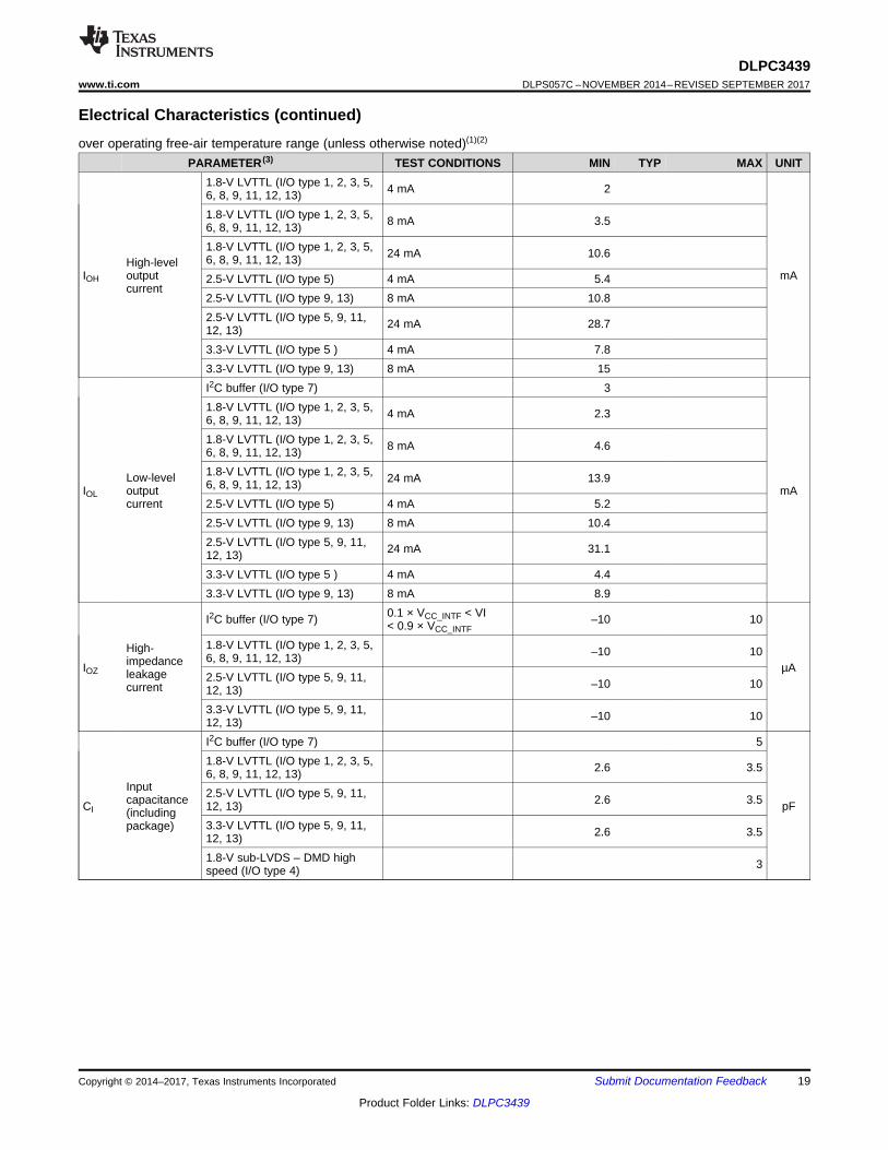
PARAMETER (3) TEST CONDITIONS MIN TYP MAX UNIT
VIH
High-levelinputthresholdvoltage
I2C buffer (I/O type 7) 0.7 × VCC_INTF(1)
V
1.8-V LVTTL (I/O type 1, 2, 3, 5,6, 8, 9, 11, 12, 13) 1.17 3.6
1.8-V LVTTL (I/O type 1, 6)identified below: (2)CMP_OUT; PARKZ; RESETZ;GPIO 0 →19
1.3 3.6
2.5-V LVTTL (I/O type 5, 9, 11,12, 13) 1.7 3.6
3.3-V LVTTL (I/O type 5, 9, 11,12, 13) 2 3.6
VIL
Low-levelinputthresholdvoltage
I2C buffer (I/O type 7) –0.5 0.3 × VCC_INTF
V
1.8-V LVTTL (I/O type 1, 2, 3, 5,6, 8, 9, 11, 12, 13) –0.3 0.63
1.8-V LVTTL (I/O type 1, 6)identified below: (2)CMP_OUT; PARKZ; RESETZ;GPIO_00 through GPIO_19
–0.3 0.5
2.5-V LVTTL (I/O type 5, 9, 11,12, 13) –0.3 0.7
3.3-V LVTTL (I/O type 5, 9, 11,12, 13) –0.3 0.8
VCM
Steady-statecommonmode voltage
1.8-V sub-LVDS (DMD highspeed)(I/O type 4)
0.8 0.9 1 mV
ǀVODǀDifferentialoutputmagnitude
1.8-V sub-LVDS (DMD highspeed)(I/O type 4)
200 mV
VOH
High-leveloutputvoltage
1.8-V LVTTL (I/O type 1, 2, 3, 5,6, 8, 9, 11, 12, 13) 1.35
V
2.5-V LVTTL (I/O type 5, 9, 11,12, 13) 1.7
3.3-V LVTTL (I/O type 5, 9, 11,12, 13) 2.4
1.8-V sub-LVDS – DMD highspeed (I/O type 4) 1
VOL
Low-leveloutputvoltage
I2C buffer (I/O type 7) VCC_INTF > 2 V 0.4
V
I2C buffer (I/O type 7) VCC_INTF < 2 V 0.2 × VCC_INTF
1.8-V LVTTL (I/O type 1, 2, 3, 5,6, 8, 9, 11, 12, 13) 0.45
2.5-V LVTTL (I/O type 5, 9, 11,12, 13) 0.7
3.3-V LVTTL (I/O type 5, 9, 11,12, 13) 0.4
1.8-V sub-LVDS – DMD highspeed (I/O type 4) 0.8
19
DLPC3439www.ti.com DLPS057C –NOVEMBER 2014–REVISED SEPTEMBER 2017
Product Folder Links: DLPC3439
Submit Documentation FeedbackCopyright © 2014–2017, Texas Instruments Incorporated
Electrical Characteristics (continued)over operating free-air temperature range (unless otherwise noted)(1)(2)
PARAMETER (3) TEST CONDITIONS MIN TYP MAX UNIT
IOH
High-leveloutputcurrent
1.8-V LVTTL (I/O type 1, 2, 3, 5,6, 8, 9, 11, 12, 13) 4 mA 2
mA
1.8-V LVTTL (I/O type 1, 2, 3, 5,6, 8, 9, 11, 12, 13) 8 mA 3.5
1.8-V LVTTL (I/O type 1, 2, 3, 5,6, 8, 9, 11, 12, 13) 24 mA 10.6
2.5-V LVTTL (I/O type 5) 4 mA 5.42.5-V LVTTL (I/O type 9, 13) 8 mA 10.82.5-V LVTTL (I/O type 5, 9, 11,12, 13) 24 mA 28.7
3.3-V LVTTL (I/O type 5 ) 4 mA 7.83.3-V LVTTL (I/O type 9, 13) 8 mA 15
IOL
Low-leveloutputcurrent
I2C buffer (I/O type 7) 3
mA
1.8-V LVTTL (I/O type 1, 2, 3, 5,6, 8, 9, 11, 12, 13) 4 mA 2.3
1.8-V LVTTL (I/O type 1, 2, 3, 5,6, 8, 9, 11, 12, 13) 8 mA 4.6
1.8-V LVTTL (I/O type 1, 2, 3, 5,6, 8, 9, 11, 12, 13) 24 mA 13.9
2.5-V LVTTL (I/O type 5) 4 mA 5.22.5-V LVTTL (I/O type 9, 13) 8 mA 10.42.5-V LVTTL (I/O type 5, 9, 11,12, 13) 24 mA 31.1
3.3-V LVTTL (I/O type 5 ) 4 mA 4.43.3-V LVTTL (I/O type 9, 13) 8 mA 8.9
IOZ
High-impedanceleakagecurrent
I2C buffer (I/O type 7) 0.1 × VCC_INTF < VI< 0.9 × VCC_INTF
–10 10
µA
1.8-V LVTTL (I/O type 1, 2, 3, 5,6, 8, 9, 11, 12, 13) –10 10
2.5-V LVTTL (I/O type 5, 9, 11,12, 13) –10 10
3.3-V LVTTL (I/O type 5, 9, 11,12, 13) –10 10
CI
Inputcapacitance(includingpackage)
I2C buffer (I/O type 7) 5
pF
1.8-V LVTTL (I/O type 1, 2, 3, 5,6, 8, 9, 11, 12, 13) 2.6 3.5
2.5-V LVTTL (I/O type 5, 9, 11,12, 13) 2.6 3.5
3.3-V LVTTL (I/O type 5, 9, 11,12, 13) 2.6 3.5
1.8-V sub-LVDS – DMD highspeed (I/O type 4) 3

20
DLPC3439DLPS057C –NOVEMBER 2014–REVISED SEPTEMBER 2017 www.ti.com
Product Folder Links: DLPC3439
Submit Documentation Feedback Copyright © 2014–2017, Texas Instruments Incorporated
(1) For the definition of VCM changes, see Figure 2.(2) Note that VOD is the differential voltage swing measured across a 100-Ω termination resistance connected directly between the
transmitter differential pins. |VOD| is the magnitude of this voltage swing relative to 0. Rise and fall times are defined for the differentialVOD signal as follows in Figure 3.
6.7 High-Speed Sub-LVDS Electrical Characteristicsover operating free-air temperature range (unless otherwise noted)
PARAMETER MIN NOM MAX UNITVCM Steady-state common mode voltage 0.8 0.9 1.0 VVCM (Δpp) (1) VCM change peak-to-peak (during switching) 75 mVVCM (Δss) (1) VCM change steady state –10 10 mV|VOD| (2) Differential output voltage magnitude 200 mVVOD (Δ) VOD change (between logic states) –10 10 mVVOH Single-ended output voltage high 1.00 VVOL Single-ended output voltage low 0.80 VtR(2) Differential output rise time 250 pstF(2) Differential output fall time 250 pstMAX Maximum switching rate 1200 MbpsDCout Output duty cycle 45% 50% 55%Txterm
(1) Internal differential termination 80 100 120 Ω
Txload100-Ω differential PCB trace(50-Ω transmission lines) 0.5 6 inches
21
DLPC3439www.ti.com DLPS057C –NOVEMBER 2014–REVISED SEPTEMBER 2017
Product Folder Links: DLPC3439
Submit Documentation FeedbackCopyright © 2014–2017, Texas Instruments Incorporated
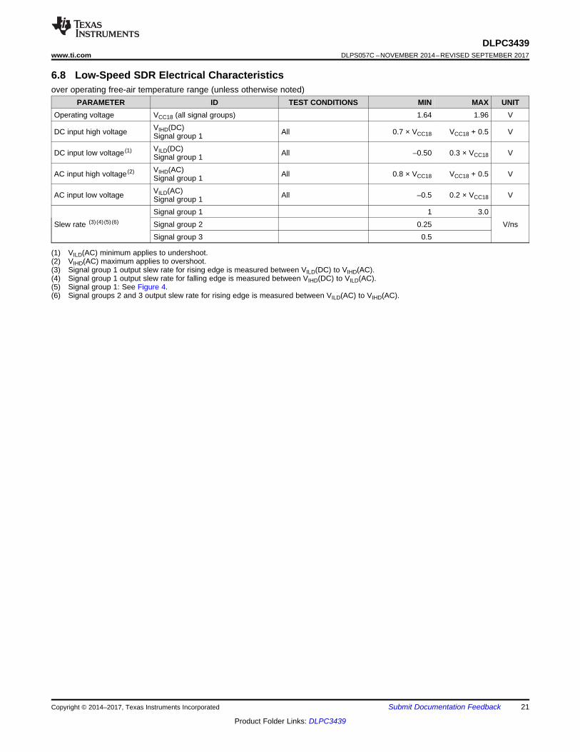
(1) VILD(AC) minimum applies to undershoot.(2) VIHD(AC) maximum applies to overshoot.(3) Signal group 1 output slew rate for rising edge is measured between VILD(DC) to VIHD(AC).(4) Signal group 1 output slew rate for falling edge is measured between VIHD(DC) to VILD(AC).(5) Signal group 1: See Figure 4.(6) Signal groups 2 and 3 output slew rate for rising edge is measured between VILD(AC) to VIHD(AC).
6.8 Low-Speed SDR Electrical Characteristicsover operating free-air temperature range (unless otherwise noted)
PARAMETER ID TEST CONDITIONS MIN MAX UNITOperating voltage VCC18 (all signal groups) 1.64 1.96 V
DC input high voltage VIHD(DC)Signal group 1 All 0.7 × VCC18 VCC18 + 0.5 V
DC input low voltage (1) VILD(DC)Signal group 1 All –0.50 0.3 × VCC18 V
AC input high voltage (2) VIHD(AC)Signal group 1 All 0.8 × VCC18 VCC18 + 0.5 V
AC input low voltage VILD(AC)Signal group 1 All –0.5 0.2 × VCC18 V
Slew rate (3) (4) (5) (6)
Signal group 1 1 3.0V/nsSignal group 2 0.25
Signal group 3 0.5

22
DLPC3439DLPS057C –NOVEMBER 2014–REVISED SEPTEMBER 2017 www.ti.com
Product Folder Links: DLPC3439
Submit Documentation Feedback Copyright © 2014–2017, Texas Instruments Incorporated
(1) The frequency accuracy for MOSC is ±200 PPM (This includes impact to accuracy due to aging, temperature, and trim sensitivity).(2) The MOSC input cannot support spread spectrum clock spreading.
6.9 System Oscillators Timing RequirementsMIN MAX UNIT
ƒclock Clock frequency, MOSC (1) 24-MHz oscillator 23.998 24.002 MHztc Cycle time, MOSC (1) 24-MHz oscillator 41.670 41.663 nstw(H) Pulse duration, MOSC, high 50% to 50% reference points (signal) 40 tc%tw(L) Pulse duration, MOSC, low 50% to 50% reference points (signal) 40 tc%tt Transition time, MOSC, tt = tƒ / tr 20% to 80% reference points (signal) 10 ns
tjpLong-term, peak-to-peak, period jitter (2), MOSC(that is the deviation in period from ideal period due solely to high frequency jitter) 2%
(1) For more information on RESETZ, see Pin Configuration and Functions.
6.10 Power-Up and Reset Timing RequirementsMIN MAX UNIT
tw(L) Pulse duration, inactive low, RESETZ 50% to 50% reference points (signal) 1.25 µstt Transition time, RESETZ (1), tt = tƒ / tr 20% to 80% reference points (signal) 0.5 µs

23
DLPC3439www.ti.com DLPS057C –NOVEMBER 2014–REVISED SEPTEMBER 2017
Product Folder Links: DLPC3439
Submit Documentation FeedbackCopyright © 2014–2017, Texas Instruments Incorporated
(1) The minimum total vertical blanking is defined by the following equation: tp_tvb(min) = 6 + [8 × Max(1, Source_ALPF/ DMD_ALPF)] lineswhere:(a) SOURCE_ALPF = Input source active lines per frame(b) DMD_ALPF = Actual DMD used lines per frame supported
(2) Total horizontal blanking is driven by the maximum line rate for a given source which will be a function of resolution and orientation. Thefollowing equation can be applied for this: tp_thb = Roundup[(1000 × ƒclock)/ LR] – APPLwhere:(a) ƒclock = Pixel clock rate in MHz(b) LR = Line rate in kHz(c) APPL is the number of active pixels per (horizontal) line.(d) If tp_thb is calculated to be less than tp_hbp + tp_hfp then the pixel clock rate is too low or the line rate is too high, and one or both
must be adjusted.
6.11 Parallel Interface Frame Timing RequirementsMIN MAX UNIT
tp_vsw Pulse duration – VSYNC_WE high 50% reference points 1 linestp_vbp Vertical back porch (VBP) – time from the leading edge of
VSYNC_WE to the leading edge HSYNC_CS for the first activeline. See (1).
50% reference points 2 lines
tp_vƒp Vertical front porch (VFP) – time from the leading edge of theHSYNC_CS following the last active line in a frame to theleading edge of VSYNC_WE. See (1).
50% reference points 1 lines
tp_tvb Total vertical blanking – time from the leading edge ofHSYNC_CS following the last active line of one frame to theleading edge of HSYNC_CS for the first active line in the nextframe. This is equal to the sum of VBP (tp_vbp) + VFP (tp_vfp).
50% reference points See (1) lines
tp_hsw Pulse duration – HSYNC_CS high 50% reference points 4 128 PCLKstp_hbp Horizontal back porch – time from rising edge of HSYNC_CS
to rising edge of DATAEN_CMD50% reference points 4 PCLKs
tp_hfp Horizontal front porch – time from falling edge ofDATAEN_CMD to rising edge of HSYNC_CS
50% reference points 8 PCLKs
tp_thb Total horizontal blanking – sum of horizontal front and backporches
50% reference points See (2) PCLKs

24
DLPC3439DLPS057C –NOVEMBER 2014–REVISED SEPTEMBER 2017 www.ti.com
Product Folder Links: DLPC3439
Submit Documentation Feedback Copyright © 2014–2017, Texas Instruments Incorporated
(1) The active (capture) edge of PCLK for HSYNC_CS, DATEN_CMD and PDATA(23:0) is software programmable, but defaults to therising edge.
(2) Clock jitter (in ns) should be calculated using this formula: Jitter = [1 / ƒclock – 5.76 ns]. Setup and hold times must be met during clockjitter.
6.12 Parallel Interface General Timing Requirements (1)
MIN MAX UNITƒclock Clock frequency, PCLK 1.0 150.0 MHztp_clkper Clock period, PCLK 50% reference points 6.66 1000 nstp_clkjit Clock jitter, PCLK Max ƒclock See (2) See (2)
tp_wh Pulse duration low, PCLK 50% reference points 2.43 nstp_wl Pulse duration high, PCLK 50% reference points 2.43 nstp_su Setup time – HSYNC_CS, DATEN_CMD,
PDATA(23:0) valid before the active edge of PCLK50% reference points 0.9 ns
tp_h Hold time – HSYNC_CS, DATEN_CMD,PDATA(23:0) valid after the active edge of PCLK
50% reference points 0.9 ns
tt Transition time – all signals 20% to 80% referencepoints
0.2 2.0 ns

20%
80%tF tR
0V
+ Vod
- Vod
Vod|Vod|
|Vod|
Vcm
Vcm(ûpp)
Vcm(ûss)
25
DLPC3439www.ti.com DLPS057C –NOVEMBER 2014–REVISED SEPTEMBER 2017
Product Folder Links: DLPC3439
Submit Documentation FeedbackCopyright © 2014–2017, Texas Instruments Incorporated
(1) Standard SPI protocol is to transmit data on the falling edge of SPI_CLK and capture data on the rising edge. The DLPC3439 doestransmit data on the falling edge, but it also captures data on the falling edge rather than the rising edge. This provides support for SPIdevices with long clock-to-Q timing. DLPC3439 hold capture timing has been set to facilitate reliable operation with standard externalSPI protocol devices.
(2) With the above output timing, DLPC3439 provides the external SPI device 8.2-ns input set-up and 8.2-ns input hold, relative to the risingedge of SPI_CLK.
(3) This range include the 200 ppm of the external oscillator (but no jitter).
6.13 Flash Interface Timing RequirementsThe DLPC3439 ASIC flash memory interface consists of a SPI flash serial interface with a programmable clock rate. TheDLPC3439 can support 1- to 64-Mb flash memories. (1) (2)
MIN MAX UNITƒclock Clock frequency, SPI_CLK See (3) 1.42 36.0 MHztp_clkper Clock period, SPI_CLK 50% reference points 704 27.7 nstp_wh Pulse duration low, SPI_CLK 50% reference points 352 nstp_wl Pulse duration high, SPI_CLK 50% reference points 352 nstt Transition time – all signals 20% to 80% reference
points0.2 3.0 ns
tp_su Setup time – SPI_DIN valid before SPI_CLK fallingedge
50% reference points 10.0 ns
tp_h Hold time – SPI_DIN valid after SPI_CLK falling edge 50% reference points 0.0 nstp_clqv SPI_CLK clock falling edge to output valid time –
SPI_DOUT and SPI_CSZ50% reference points 1.0 ns
tp_clqx SPI_CLK clock falling edge output hold time –SPI_DOUT and SPI_CSZ
50% reference points –3.0 3.0 ns
Figure 2. Definition of VCM Changes
NOTE: VCM is removed when the signals are viewed differentially.
Figure 3. Differential Output Signal

tw(L)
RESETZ80%50%20%
DC Power Supplies
80%50%20%
80%50%20%
80%50%20%
tw(L) tw(L)
tt tt
MOSC 50%
80%
20%50%
50%
tc
tw(H) tw(L)
tt
80%
20%
tt
26
DLPC3439DLPS057C –NOVEMBER 2014–REVISED SEPTEMBER 2017 www.ti.com
Product Folder Links: DLPC3439
Submit Documentation Feedback Copyright © 2014–2017, Texas Instruments Incorporated
Figure 4. Low Speed (LS) I/O Input Thresholds
Figure 5. System Oscillators
Figure 6. Power-Up and Power-Down RESETZ Timing

PCLK
tp_sutp_h
tp_wh tp_wl
tp_clkper
VSYNC_WE
HSYNC_CS
DATAEN_CMD
tp_vsw
1 Frame
tp_vbp tp_vfp
HSYNC_CS
DATAEN_CMD
tp_hsw
1 Line
tp_hfptp_hbp
PDATA(23/15:0) P0
PCLK
P1 P2 P3P
n-2P
n-1Pn
(This diagram assumes the VSYNC active edge is the rising edge)
(This diagram assumes the HSYNC active edge is the rising edge)
27
DLPC3439www.ti.com DLPS057C –NOVEMBER 2014–REVISED SEPTEMBER 2017
Product Folder Links: DLPC3439
Submit Documentation FeedbackCopyright © 2014–2017, Texas Instruments Incorporated
Figure 7. Parallel Interface Frame Timing
Figure 8. Parallel Interface General Timing

SPI_CLK
(ASIC Output)
SPI_DIN
(ASIC Inputs)
SPI_DOUT, SPI_CS(1:0)
(ASIC Outputs)
tp_h
tclkper
twh
twl
tp_su
tp_clqx
tp_clqv
28
DLPC3439DLPS057C –NOVEMBER 2014–REVISED SEPTEMBER 2017 www.ti.com
Product Folder Links: DLPC3439
Submit Documentation Feedback Copyright © 2014–2017, Texas Instruments Incorporated
Figure 9. Flash Interface Timing
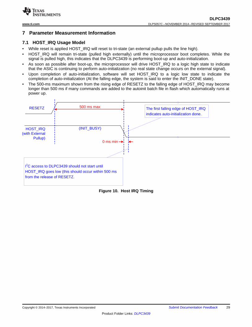
RESETZ 500 ms max
I2C access to DLPC3439 should not start until HOST_IRQ goes low (this should occur within 500 ms from the release of RESETZ.
HOST_IRQ(with External
Pullup)0 ms min
(INIT_BUSY)
The first falling edge of HOST_IRQ indicates auto-initialization done.
29
DLPC3439www.ti.com DLPS057C –NOVEMBER 2014–REVISED SEPTEMBER 2017
Product Folder Links: DLPC3439
Submit Documentation FeedbackCopyright © 2014–2017, Texas Instruments Incorporated
7 Parameter Measurement Information
7.1 HOST_IRQ Usage Model• While reset is applied HOST_IRQ will reset to tri-state (an external pullup pulls the line high).• HOST_IRQ will remain tri-state (pulled high externally) until the microprocessor boot completes. While the
signal is pulled high, this indicates that the DLPC3439 is performing boot-up and auto-initialization.• As soon as possible after boot-up, the microprocessor will drive HOST_IRQ to a logic high state to indicate
that the ASIC is continuing to perform auto-initialization (no real state change occurs on the external signal).• Upon completion of auto-initialization, software will set HOST_IRQ to a logic low state to indicate the
completion of auto-initialization (At the falling edge, the system is said to enter the INIT_DONE state).• The 500-ms maximum shown from the rising edge of RESETZ to the falling edge of HOST_IRQ may become
longer than 500 ms if many commands are added to the autoinit batch file in flash which automatically runs atpower up.
Figure 10. Host IRQ Timing

30
DLPC3439DLPS057C –NOVEMBER 2014–REVISED SEPTEMBER 2017 www.ti.com
Product Folder Links: DLPC3439
Submit Documentation Feedback Copyright © 2014–2017, Texas Instruments Incorporated
7.2 Input Source
7.2.1 Input Source - Frame RatesThe dual DLPC3439s will support both 2D and 3D sources on the parallel interface. The DLPC3439s have verylimited scaling capabilities, but a limited number of input image sizes can be scaled up to 1920×1080 fordisplaying images on the DMD over the frame rates given below for 2D sources and 3D sources.
For 2D sources, the following two input options are supported on the parallel interface:• 1920×1080 over 10-62 Hz• 1280×720 over 10-62 Hz (Image will be scaled up to 1920×1080)
The DLPC3439s have a 150 MHz maximum input clock frequency for the parallel interface which means thatpixel inputs cannot be supported at 120 Hz for 1920×1080. However, up to 120-Hz 3D can be supported if thevertical and/or horizontal resolution of the input source is reduced. The DLPC3439s can then scale the imagesup to 1920×1080 for displaying them on the DMD. For 3D sources, the following three input options aresupported on the parallel interface and all will be scaled up to 1920×1080:• 1920×540 over 98-102 Hz and 118-122 Hz• 960×1080 over 98-102 Hz and 118-122 Hz• 1280×720 over 98-102 Hz and 118-122 Hz
For 3D sources on the parallel interface, images must be frame-sequential (L, R, L, …) when input to theDLPC3439s. Any processing required to unpack 3D images and to convert them to frame sequential must bedone by external electronics prior to inputting the images to the DLPC3439s. Each 3D source frame input on theparallel interface must contain a single eye frame of data separated by a VSYNC where an eye frame containsimage data for a single left or right eye. The signal 3DR input to the DLPC3439s tells whether the input frame isfor the left eye or right eye.
For 3D sources, each DMD frame will be displayed at the same rate as the parallel interface frame rate. Typicaltiming for 50-Hz or 60-Hz 3D HDMI source frames, the parallel interface of the DLPC3439s, and the DMD isshown in Figure 11. GPIO_09 is optionally sent to a transmitter on the system PCB for wirelessly transmitting async signal to 3D glasses. The glasses are then in phase with the DMD images being displayed. Alternately, 3-DGlasses Operation shows how DLP Link pulses can be used instead.
Figure 11. DLPC3439 L/R Frame and Signals Timing
7.2.2 Parallel Interface Supports Six Data Transfer FormatsThe six data transfer formats supported by the parallel interface are:• 24-bit RGB888 or 24-bit YCrCb888 on a 24 data wire interface• 18-bit RGB666 or 18-bit YCrCb666 on a 18 data wire interface• 16-bit RGB565 or 16-bit YCrCb565 on a 16 data wire interface

7 6 5 4 3 2 1 0 7 6 5 4 3 2 1 0
23 0YCr / Cb N/A
ASIC Input
Mapping
ASIC Internal Re-
Mapping7 6 5 4 3 2 1 0 7 6 5 4 3 2 1 0 7 6 5 4 3 2 1 0
YCr/Cb n/a
7 6 5 4 3 2 1 0
23 0
7 6 5 4 3 2 1 0 7 6 5 4 3 2 1 0 7 6 5 4 3 2 1 0
Green / YRed / Cr Blue / Cb
Input Input
7 6 5 4 3 2 1 07 6 5 4 3 2 1 07 6 5 4 3 2 1 0
Input
ASIC Internal Re-
Mapping
ASIC Input
Mapping
23 0Input Input
7 6 5 4 3 2 1 0 7 6 5 4 3 2 1 0 7 6 5 4 3 2 1 0
Green / YRed / Cr Blue / Cb
7 6 5 4 3 2 1 07 6 5 4 3 2 1 07 6 5 4 3 2 1 0
InputASIC Input
Mapping
ASIC Internal Re-
Mapping
7 6 5 4 3 2 1 0 7 6 5 4 3 2 1 0 7 6 5 4 3 2 1 0
23 0Green / YRed / Cr Blue / Cb
7 6 5 4 3 2 1 0 7 6 5 4 3 2 1 0 7 6 5 4 3 2 1 0
Green / YRed / Cr Blue / Cb
ASIC Input
Mapping
ASIC Internal Re-
Mapping
31
DLPC3439www.ti.com DLPS057C –NOVEMBER 2014–REVISED SEPTEMBER 2017
Product Folder Links: DLPC3439
Submit Documentation FeedbackCopyright © 2014–2017, Texas Instruments Incorporated
Input Source (continued)• 16-bit YCrCb 4:2:2 (standard sampling assumed to be Y0Cb0, Y1Cr0, Y2Cb2, Y3Cr2, Y4Cb4, Y5Cr4, …)
PDATA Bus – Parallel Interface Bit Mapping Modes shows the required PDATA(23:0) bus mapping for these sixdata transfer formats.
7.2.2.1 PDATA Bus – Parallel Interface Bit Mapping Modes
Figure 12. RGB-888 / YCrCb-888 I/O Mapping
Figure 13. RGB-666 / YCrCb-666 I/O Mapping
Figure 14. RGB-565 / YCrCb-565 I/O Mapping
Figure 15. 16-Bit YCrCb-880 I/O Mapping

ARM Cortex M3 128KB I/D MemoryI2C_0
SPI_0
GPIOSPI_1I2C_1
LED ControlOther options
20
Input Control
Processing24
Parallel Interface
5
Test Pattern
Generator
Clocks & Reset
Generation
Real Time Control System
DLPTM Display Formatting
eDRAM(Frame Memory)
DMD I/F
DMD_HS_CLK (sub-LVDS)DMD_HS_DATA(A:H) (sub-LVDS)DMD_LS_CLKDMD_LS_WDATADMD_LS_RDATADMD_DEN_ARSTZ
SplashScreen
- Chroma Interpolation- Color Space Conversion- Brightness Enhancement- Dynamic Scaling- Keystone Correction- Gamma Correction
Video Processing
- Image Format Processing- Contrast Adjust- Color Correction- CAIC Processing- Blue Noise STM- Power Saving Operations
Clock (Crystal)Reset Control
32
DLPC3439DLPS057C –NOVEMBER 2014–REVISED SEPTEMBER 2017 www.ti.com
Product Folder Links: DLPC3439
Submit Documentation Feedback Copyright © 2014–2017, Texas Instruments Incorporated
8 Detailed Description
8.1 OverviewThe DLPC3439 is the display controller for the DLP4710 (0.47 1080p) DMD. The DLPC3439 is part of thechipset comprising two DLPC3439 controllers, the DLP4710 (0.47 1080p) DMD, and the DLPA3000 orDLPA3005 PMIC/LED driver. All four components of the chipset must be used in conjunction with each other forreliable operation of the DLP4710 (0.47 1080p) DMD. Each DLPC3439 display controller provides interfaces anddata/image processing functions that are optimized for small form factor and power-constrained displayapplications. Applications include pico projectors, wearable displays, and digital signage. Standalone projectorsmust include a separate front-end chip to interface to the outside world (for example, video decoder, HDMIreceiver, triple ADC, or USB I/F chip).
8.2 Functional Block Diagram
8.3 Feature Description
8.3.1 Interface Timing RequirementsThis section defines the timing requirements for the external interfaces for the DLPC3439 ASIC.
8.3.1.1 Parallel InterfaceThe parallel interface complies with the standard graphics interface protocol, which includes a vertical sync signal(VSYNC_WE), horizontal sync signal (HSYNC_CS), optional data valid signal (DATAEN_CMD), a 24-bit databus (PDATA), and a pixel clock (PCLK). The polarity of both syncs and the active edge of the clock areprogrammable. Figure 7 shows the relationship of these signals. The data valid signal (DATAEN_CMD) isoptional in that the DLPC3439 provides auto-framing parameters that can be programmed to define the datavalid window based on pixel and line counting relative to the horizontal and vertical syncs.
In addition to these standard signals, an optional side-band signal (PDM_CVS_TE) is available, which allowsperiodic frame updates to be stopped without losing the displayed image. When PDM_CVS_TE is active, it actsas a data mask and does not allow the source image to be propagated to the display. A programmable PDMpolarity parameter determines if it is active high or active low. This parameter defaults to make PDM_CVS_TEactive high; if this function is not desired, then it should be tied to a logic low on the PCB. PDM_CVS_TE isrestricted to change only during vertical blanking.
33
DLPC3439www.ti.com DLPS057C –NOVEMBER 2014–REVISED SEPTEMBER 2017
Product Folder Links: DLPC3439
Submit Documentation FeedbackCopyright © 2014–2017, Texas Instruments Incorporated
Feature Description (continued)
NOTEVSYNC_WE must remain active at all times (in lock-to-VSYNC mode) or the displaysequencer will stop and cause the LEDs to be turned off.
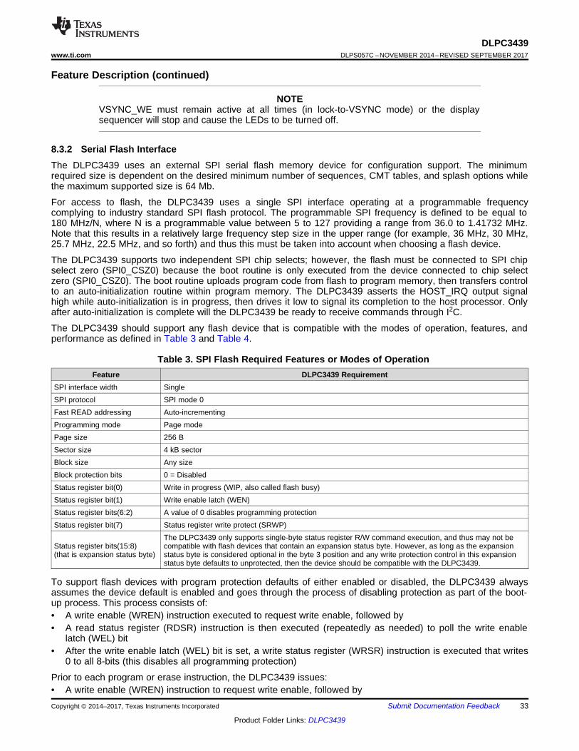
8.3.2 Serial Flash InterfaceThe DLPC3439 uses an external SPI serial flash memory device for configuration support. The minimumrequired size is dependent on the desired minimum number of sequences, CMT tables, and splash options whilethe maximum supported size is 64 Mb.
For access to flash, the DLPC3439 uses a single SPI interface operating at a programmable frequencycomplying to industry standard SPI flash protocol. The programmable SPI frequency is defined to be equal to180 MHz/N, where N is a programmable value between 5 to 127 providing a range from 36.0 to 1.41732 MHz.Note that this results in a relatively large frequency step size in the upper range (for example, 36 MHz, 30 MHz,25.7 MHz, 22.5 MHz, and so forth) and thus this must be taken into account when choosing a flash device.
The DLPC3439 supports two independent SPI chip selects; however, the flash must be connected to SPI chipselect zero (SPI0_CSZ0) because the boot routine is only executed from the device connected to chip selectzero (SPI0_CSZ0). The boot routine uploads program code from flash to program memory, then transfers controlto an auto-initialization routine within program memory. The DLPC3439 asserts the HOST_IRQ output signalhigh while auto-initialization is in progress, then drives it low to signal its completion to the host processor. Onlyafter auto-initialization is complete will the DLPC3439 be ready to receive commands through I2C.
The DLPC3439 should support any flash device that is compatible with the modes of operation, features, andperformance as defined in Table 3 and Table 4.
Table 3. SPI Flash Required Features or Modes of OperationFeature DLPC3439 Requirement
SPI interface width SingleSPI protocol SPI mode 0Fast READ addressing Auto-incrementingProgramming mode Page modePage size 256 BSector size 4 kB sectorBlock size Any sizeBlock protection bits 0 = DisabledStatus register bit(0) Write in progress (WIP, also called flash busy)Status register bit(1) Write enable latch (WEN)Status register bits(6:2) A value of 0 disables programming protectionStatus register bit(7) Status register write protect (SRWP)
Status register bits(15:8)(that is expansion status byte)
The DLPC3439 only supports single-byte status register R/W command execution, and thus may not becompatible with flash devices that contain an expansion status byte. However, as long as the expansionstatus byte is considered optional in the byte 3 position and any write protection control in this expansionstatus byte defaults to unprotected, then the device should be compatible with the DLPC3439.
To support flash devices with program protection defaults of either enabled or disabled, the DLPC3439 alwaysassumes the device default is enabled and goes through the process of disabling protection as part of the boot-up process. This process consists of:• A write enable (WREN) instruction executed to request write enable, followed by• A read status register (RDSR) instruction is then executed (repeatedly as needed) to poll the write enable
latch (WEL) bit• After the write enable latch (WEL) bit is set, a write status register (WRSR) instruction is executed that writes
0 to all 8-bits (this disables all programming protection)
Prior to each program or erase instruction, the DLPC3439 issues:• A write enable (WREN) instruction to request write enable, followed by

34
DLPC3439DLPS057C –NOVEMBER 2014–REVISED SEPTEMBER 2017 www.ti.com
Product Folder Links: DLPC3439
Submit Documentation Feedback Copyright © 2014–2017, Texas Instruments Incorporated
(1) Only the first data byte is shown, data continues.(2) DLPC3439 does not support access to a second/expansion Write Status byte.
• A read status register (RDSR) instruction (repeated as needed) to poll the write enable latch (WEL) bit• After the write enable latch (WEL) bit is set, the program or erase instruction is executed• Note the flash automatically clears the write enable status after each program and erase instruction
The specific instruction OpCode and timing compatibility requirements are listed in Table 4 and Table 5. Notehowever that the DLPC3439 does not read the flash’s electronic signature ID and thus cannot automaticallyadapt protocol and clock rate based on the ID.
Table 4. SPI Flash Instruction OpCode and Access Profile Compatibility Requirements
SPI Flash Command First Byte(OPCODE) Second Byte Third Byte Fourth Byte Fifth Byte Sixth Byte
Fast READ (1 Output) 0x0B ADDRS(0) ADDRS(1) ADDRS(2) dummy DATA(0) (1)
Read status 0x05 n/a n/a STATUS(0)Write status 0x01 STATUS(0) (2)
Write enable 0x06Page program 0x02 ADDRS(0) ADDRS(1) ADDRS(2) DATA(0) (1)
Sector erase (4KB) 0x20 ADDRS(0) ADDRS(1) ADDRS(2)Chip erase 0xC7
(1) The timing values are related to the specification of the flash device itself, not the DLPC3439.(2) The DLPC3439 does not drive the HOLD or WP (active low write protect) pins on the flash device, and thus these pins should be tied to
a logic high on the PCB through an external pullup.
The specific and timing compatibility requirements for a DLPC3439 compatible flash are listed in Table 5 andTable 6.
Table 5. SPI Flash Key Timing Parameter Compatibility Requirements (1) (2)
SYMBOL ALTERNATESYMBOL MIN MAX UNIT
FR ƒCAccess frequency(all commands) ≤1.42 MHz
tSHSL tCSHChip select high time (also called chip select deselecttime) ≤200 ns
tCLQX tHO Output hold time ≥0 nstCLQV tV Clock low to output valid time ≤11 nstDVCH tDSU Data in set-up time ≤5 nstCHDX tDH Data in hold time ≤5 ns
The DLPC3439 supports 1.8-, 2.5-, or 3.3-V serial flash devices. To do so, VCC_FLSH must be supplied with thecorresponding voltage. Table 6 contains a list of 1.8-, 2.5-, and 3.3-V compatible SPI serial flash devicessupported by the DLPC3439.

35
DLPC3439www.ti.com DLPS057C –NOVEMBER 2014–REVISED SEPTEMBER 2017
Product Folder Links: DLPC3439
Submit Documentation FeedbackCopyright © 2014–2017, Texas Instruments Incorporated
(1) The flash supply voltage must match VCC_FLSH on the DLPC3439. Special attention is needed when ordering devices to ensure thedesired supply voltage is attained as multiple voltage options are often available under the same base part number.
(2) Beware when considering Numonyx (Micron) serial flash devices as they typically do not have the 4 kB sector size needed to beDLPC3439 compatible.
(3) All of the flash devices shown are compatible with the DLPC3439, but only those marked with 'Yes' in the DVT column have beenvalidated during TI Validation testing using a TI reference design. Those marked with 'No' can be used at the original designmanufacturer (ODM)’s own risk. Other parts aside from those shown can be used if the timing conditions in Serial Flash Interface aremet.
8.3.3 Tested Flash Devices
Table 6. DLPC3439 Compatible SPI Flash Device Options (3.3-V Compatible Devices) (1) (2)
DVT(3) DENSITY (Mb) VENDOR PART NUMBER PACKAGE SIZEYes 32 Mb Winbond W25Q32FVSSIG 5.2 mm x 7.9 mm, 8-pin SOICYes 64 Mb Winbond W25Q64FVSSIG 5.2 mm x 7.9 mm, 8-pin SOICYes 32 Mb Macronix MX25L3233FM2I-08G 5.2 mm x 7.9 mm, 8-pin SOPYes 64 Mb Macronix MX25L6433FM2I-08G 5.2 mm x 7.9 mm, 8-pin SOP
8.3.4 Serial Flash ProgrammingNote that the flash can be programmed through the DLPC3439 over I2C or by driving the SPI pins of the flashdirectly while the DLPC3439 I/O are tri-stated. SPI0_CLK, SPI0_DOUT, and SPI0_CSZ0 I/O can be tri-stated byholding RESETZ in a logic low state while power is applied to the DLPC3439. Note that SPI0_CSZ1 is not tri-stated by this same action.
8.3.5 SPI Signal RoutingThe DLPC3439 is designed to support two SPI slave devices on the SPI0 interface, specifically a serial flash andthe DLPA3000 or DLPA3005. This requires routing associated SPI signals to two locations while attempting tooperate up to 36 MHz. Take special care to ensure that reflections do not compromise signal integrity. To thisend, the following recommendations are provided:• The SPI0_CLK PCB signal trace from the DLPC3439 source to each slave device should be split into
separate routes as close to the DLPC3439 as possible. In addition, the SPI0_CLK trace length to each deviceshould be equal in total length.
• The SPI0_DOUT PCB signal trace from the DLPC3439 source to each slave device should be split intoseparate routes as close to the DLPC3439 as possible. In addition, the SPI0_DOUT trace length to eachdevice should be equal in total length (use the same strategy as SPI0_CLK).
• The SPI0_DIN PCB signal trace from each slave device to the point where they intersect on their way back tothe DLPC3439 should be made equal in length and as short as possible. They should then share a commontrace back to the DLPC3439.
• SPI0_CSZ0 and SPI0_CSZ1 need no special treatment because they are dedicated signals which drive onlyone device.
8.3.6 I2C Interface PerformanceBoth DLPC3439 I2C interface ports support a 100-kHz baud rate. By definition, I2C transactions operate at thespeed of the slowest device on the bus, thus there is no requirement to match the speed grade of all devices inthe system.
8.3.7 Content-Adaptive Illumination ControlContent-adaptive illumination control (CAIC) is an image processing algorithm that takes advantage of the factthat in common real-world image content, most pixels in the images are well below full scale for the for the R, G,and B digital channels being input to the DLPC3439. As a result of this, the average picture level (APL) for theoverall image is also well below full scale, and the system’s dynamic range for the collective set of pixel values isnot fully utilized. CAIC takes advantage of this headroom between the source image APL and the top of theavailable dynamic range of the display system.

36
DLPC3439DLPS057C –NOVEMBER 2014–REVISED SEPTEMBER 2017 www.ti.com
Product Folder Links: DLPC3439
Submit Documentation Feedback Copyright © 2014–2017, Texas Instruments Incorporated
CAIC evaluates images frame by frame and derives three unique digital gains, one for each of the R, G, and Bcolor channels. During CAIC image processing, each gain is applied to all pixels in the associated color channel.CAIC derives each color channel’s gain that is applied to all pixels in that channel so that the pixels as a groupcollectively shift upward and as close to full scale as possible. To prevent any image quality degradation, thegains are set at the point where just a few pixels in each color channel are clipped. Figure 16 and Figure 17show an example of the application of CAIC for one color channel.
Figure 16. Input Pixels Example
Figure 17. Displayed Pixels After CAIC Processing
Figure 17 shows the gain that is applied to a color processing channel inside the DLPC3439. CAIC will alsoadjust the power for the R, G, and B LED. For each color channel of an individual frame, CAIC will intelligentlydetermine the optimal combination of digital gain and LED power. The decision regarding how much digital gainto apply to a color channel and how much to adjust the LED power for that color is heavily influenced by thesoftware command settings sent to the DLPC3439 for configuring CAIC.
As CAIC applies a digital gain to each color channel independently and adjusts each LED’s power independently,CAIC also makes sure that the resulting color balance in the final image matches the target color balance for theprojector system. Thus, the effective displayed white point of images is held constant by CAIC from frame toframe.
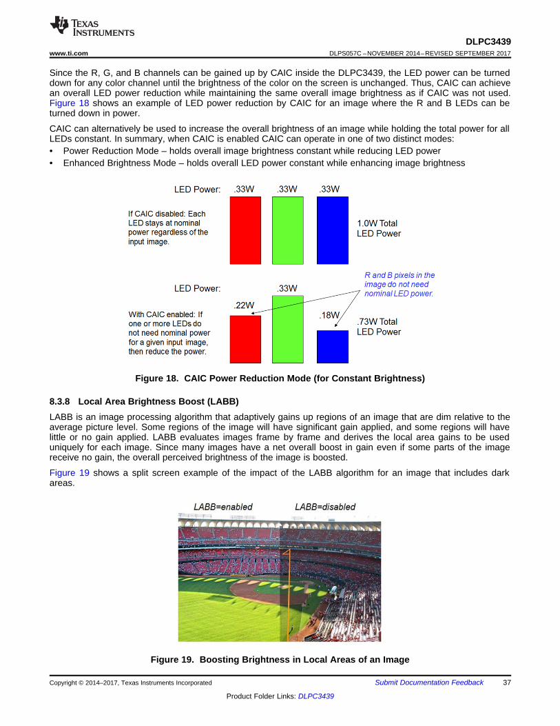
37
DLPC3439www.ti.com DLPS057C –NOVEMBER 2014–REVISED SEPTEMBER 2017
Product Folder Links: DLPC3439
Submit Documentation FeedbackCopyright © 2014–2017, Texas Instruments Incorporated
Since the R, G, and B channels can be gained up by CAIC inside the DLPC3439, the LED power can be turneddown for any color channel until the brightness of the color on the screen is unchanged. Thus, CAIC can achievean overall LED power reduction while maintaining the same overall image brightness as if CAIC was not used.Figure 18 shows an example of LED power reduction by CAIC for an image where the R and B LEDs can beturned down in power.
CAIC can alternatively be used to increase the overall brightness of an image while holding the total power for allLEDs constant. In summary, when CAIC is enabled CAIC can operate in one of two distinct modes:• Power Reduction Mode – holds overall image brightness constant while reducing LED power• Enhanced Brightness Mode – holds overall LED power constant while enhancing image brightness
Figure 18. CAIC Power Reduction Mode (for Constant Brightness)
8.3.8 Local Area Brightness Boost (LABB)LABB is an image processing algorithm that adaptively gains up regions of an image that are dim relative to theaverage picture level. Some regions of the image will have significant gain applied, and some regions will havelittle or no gain applied. LABB evaluates images frame by frame and derives the local area gains to be useduniquely for each image. Since many images have a net overall boost in gain even if some parts of the imagereceive no gain, the overall perceived brightness of the image is boosted.
Figure 19 shows a split screen example of the impact of the LABB algorithm for an image that includes darkareas.
Figure 19. Boosting Brightness in Local Areas of an Image

38
DLPC3439DLPS057C –NOVEMBER 2014–REVISED SEPTEMBER 2017 www.ti.com
Product Folder Links: DLPC3439
Submit Documentation Feedback Copyright © 2014–2017, Texas Instruments Incorporated
LABB works best when the decision about the strength of gains used is determined by ambient light conditions.For this reason, an ambient light sensor can be read by an external processor for each frame. Based on thesensor readings, the external processor can send LABB strength commands to apply higher gains for brightrooms to help overcome any washing out of images. LABB will receive commands to apply lower gains in darkrooms to prevent over-punching of images.
8.3.9 3-D Glasses OperationFor supporting 3D glasses, the DLPC3439-based chip set outputs sync information to synchronize the Lefteye/Right eye shuttering in the glasses with the displayed DMD image frames.
Two different types of glasses are often used to achieve synchronization. One relies on an IR transmitter on thesystem PCB to send an IR sync signal to an IR receiver in the glasses. In this case, the DLPC3439 output signalGPIO_09 can be used to cause the IR transmitter to send an IR sync signal to the glasses. The timing for signalGPIO_09 is shown in Figure 11.
The second type of glasses relies on sync information that is encoded into the light being output from theprojection lens. This is referred to as the DLP Link approach for 3D, and many 3D glasses from differentsuppliers have been built using this method. This demonstrates that the DLP Link method can work reliably. Theadvantage of the DLP Link approach is that it takes advantage of existing projector hardware to transmit the syncinformation to the glasses. This can save on cost, size, and power in the projector.
For generating the DLP Link sync information, one light pulse per DMD frame is output from the projection lenswhile the glasses have both shutters closed. To achieve this, the DLPC3439 will tell the DLPA3000 or DLPA3005when to turn on the illumination source (typically LEDs or lasers) so that an encoded light pulse is output onceper DMD frame. Since the shutters in the glasses are both off when the DLP Link pulse is sent, the projectorillumination source will also be off except for the when light is sent to create the DLP Link pulse. The timing forthe light pulses for DLP Link 3D operation is shown in Figure 20 and Figure 21.
Figure 20. DLPC3439 L/R Timing for DLP Link

B
CE
D
VideoVideo A A
Pulse position changes on alternate subframes
Bothshuttersoff
Nextshutteron
39
DLPC3439www.ti.com DLPS057C –NOVEMBER 2014–REVISED SEPTEMBER 2017
Product Folder Links: DLPC3439
Submit Documentation FeedbackCopyright © 2014–2017, Texas Instruments Incorporated
(1) Timing parameter C is always the sum of B+D.
NOTE: The period between DLPLink pulses alternates between the subframe period + D and the subframe period – D, whereD is the delta period.
Figure 21. 3D DLP Link Pulse Timing
Table 7. 3D DLP Link Nominal Timing Table (1)
HDMI SOURCE REFERENCE(Hz)
3D DMD SEQUENCE RATE(Hz)
A(µs)
B(µs)
C(µs)
D(µs)
E(µs)
49.0 98 31.8 >500 >622 161.6 >200050.0 100 31.2 >500 >658 158.4 >200051.0 102 30.6 >500 >655 155.3 >200059.0 118 26.4 >500 >634 134.2 >200060.0 120 26.0 >500 >632 132.0 >200061.0 122 25.6 >500 >630 129.8 >2000
(1) Timing parameter C is always the sum of B+D.
Table 8. 3D DLP Link Min/Max Timing Table (1)
HDMI SOURCE REFERENCE(Hz)
3D DMD SEQUENCE RATE(Hz)
A(µs)
B(µs)
C(µs)
D(µs)
E(µs)
49.0 98 20-32 >500 >628 128-163 >200050.0 100 20-32 >500 >628 128-163 >200051.0 102 20-32 >500 >628 128-163 >200059.0 118 20-32 >500 >628 128-163 >200060.0 120 20-32 >500 >628 128-163 >200061.0 122 20-32 >500 >628 128-163 >2000
8.3.10 DMD (Sub-LVDS) InterfaceThe DLPC3439 ASIC DMD interface consists of a HS 1.8-V sub-LVDS output only interface with a maximumclock speed of 600-MHz DDR and a LS SDR (1.8-V LVCMOS) interface with a fixed clock speed of 120 MHz.Table 9 shows how the 8 sub-LVDS lanes are configured for the DLP4710 (.47 1080p) DMD.
Table 9. DLP4710 (.47 1080p) DMD – ASIC to 8-Lane DMD Pin MappingDLPC3439 ASIC 8 LANE DMD ROUTING OPTIONS
DMD PINSMASTER DLPC3439 CONFIGURATIONSwap Control = x0
SLAVE DLPC3439 CONFIGURATIONSwap Control = x2
HS_WDATA_D_PHS_WDATA_D_N
HS_WDATA_E_PHS_WDATA_E_N
Input DATA_p_0Input DATA_n_0
HS_WDATA_C_PHS_WDATA_C_N
HS_WDATA_F_PHS_WDATA_F_N
Input DATA_p_1Input DATA_n_1

40
DLPC3439DLPS057C –NOVEMBER 2014–REVISED SEPTEMBER 2017 www.ti.com
Product Folder Links: DLPC3439
Submit Documentation Feedback Copyright © 2014–2017, Texas Instruments Incorporated
Table 9. DLP4710 (.47 1080p) DMD – ASIC to 8-Lane DMD Pin Mapping (continued)DLPC3439 ASIC 8 LANE DMD ROUTING OPTIONS
DMD PINSMASTER DLPC3439 CONFIGURATIONSwap Control = x0
SLAVE DLPC3439 CONFIGURATIONSwap Control = x2
HS_WDATA_B_PHS_WDATA_B_N
HS_WDATA_G_PHS_WDATA_G_N
Input DATA_p_2Input DATA_n_2
HS_WDATA_A_PHS_WDATA_A_N
HS_WDATA_H_PHS_WDATA_H_N
Input DATA_p_3Input DATA_n_3
HS_WDATA_H_PHS_WDATA_H_N
HS_WDATA_A_PHS_WDATA_A_N
Input DATA_p_4Input DATA_n_4
HS_WDATA_G_PHS_WDATA_G_N
HS_WDATA_B_PHS_WDATA_B_N
Input DATA_p_5Input DATA_n_5
HS_WDATA_F_PHS_WDATA_F_N
HS_WDATA_C_PHS_WDATA_C_N
Input DATA_p_6Input DATA_n_6
HS_WDATA_E_PHS_WDATA_E_N
HS_WDATA_D_PHS_WDATA_D_N
Input DATA_p_7Input DATA_n_7
8.3.11 Calibration and Debug SupportThe DLPC3439 contains a test point output port, TSTPT_(7:0), which provides selected system calibrationsupport as well as ASIC debug support. These test points are inputs while reset is applied and switched tooutputs when reset is released. The state of these signals is sampled upon the release of system reset and thecaptured value configures the test mode until the next time reset is applied. Each test point includes an internalpulldown resistor, thus external pullups must be used to modify the default test configuration. The defaultconfiguration (x000) corresponds to the TSTPT_(7:0) outputs remaining tri-stated to reduce switching activityduring normal operation. For maximum flexibility, an option to jumper to an external pullup is recommended forTSTPT_(2:0). Pullups on TSTPT_(6:3) are used to configure the ASIC for a specific mode or option. TI does notrecommend adding pullups to TSTPT_(7:3) because this has adverse effects for normal operation. This externalpullup is only sampled upon a 0-to-1 transition on the RESETZ input, thus changing their configuration after resetis released will not have any effect until the next time reset is asserted and released. Table 10 defines the testmode selection for one programmable scenario defined by TSTPT(2:0).
(1) These are only the default output selections. Software can reprogram the selection at any time.
Table 10. Test Mode Selection Scenario Defined by TSTPT(2:0) (1)
TSTPT(2:0) CAPTURE VALUE NO SWITCHING ACTIVITYx000
CLOCK DEBUG OUTPUTx010
TSTPT(0) HI-Z 60 MHzTSTPT(1) HI-Z 30 MHzTSTPT(2) HI-Z 0.7 to 22.5 MHzTSTPT(3) HI-Z HIGHTSTPT(4) HI-Z LOWTSTPT(5) HI-Z HIGHTSTPT(6) HI-Z HIGHTSTPT(7) HI-Z 7.5 MHz
8.3.12 DMD Interface ConsiderationsThe sub-LVDS HS interface waveform quality and timing on the DLPC3439 ASIC is dependent on the totallength of the interconnect system, the spacing between traces, the characteristic impedance, etch losses, andhow well matched the lengths are across the interface. Thus, ensuring positive timing margin requires attentionto many factors.
As an example, DMD interface system timing margin can be calculated as follows:Setup Margin = (DLPC3439 output setup) – (DMD input setup) – (PCB routing mismatch) – (PCB SI degradation) (1)Hold-time Margin = (DLPC3439 output hold) – (DMD input hold) – (PCB routing mismatch) – (PCB SI degradation)
Where PCB SI degradation is signal integrity degradation due to PCB effects which includes such things asSimultaneously Switching Output (SSO) noise, cross-talk and Inter-symbol Interference (ISI) noise. (2)

41
DLPC3439www.ti.com DLPS057C –NOVEMBER 2014–REVISED SEPTEMBER 2017
Product Folder Links: DLPC3439
Submit Documentation FeedbackCopyright © 2014–2017, Texas Instruments Incorporated
DLPC3439 I/O timing parameters as well as DMD I/O timing parameters can be found in their correspondingdata sheets. Similarly, PCB routing mismatch can be budgeted and met through controlled PCB routing.However, PCB SI degradation is a more complicated adjustment.
In an attempt to minimize the signal integrity analysis that would otherwise be required, the following PCB designguidelines are provided as a reference of an interconnect system that will satisfy both waveform quality andtiming requirements (accounting for both PCB routing mismatch and PCB SI degradation). Variation from theserecommendations may also work, but should be confirmed with PCB signal integrity analysis or labmeasurements.
LEFT: DMD_HS Differential Signals RIGHT: DMD_LS Signals
Figure 22. DMD Interface Board Stack-Up Details
8.4 Device Functional ModesThe DLPC3439 has two functional modes (ON/OFF) controlled by a single pin PROJ_ON:• When pin PROJ_ON is set high, the projector automatically powers up and an image is projected from the
DMD.• When pin PROJ_ON is set low, the projector automatically powers down and only microwatts of power are
consumed.

42
DLPC3439DLPS057C –NOVEMBER 2014–REVISED SEPTEMBER 2017 www.ti.com
Product Folder Links: DLPC3439
Submit Documentation Feedback Copyright © 2014–2017, Texas Instruments Incorporated
9 Application and Implementation
NOTEInformation in the following applications sections is not part of the TI componentspecification, and TI does not warrant its accuracy or completeness. TI’s customers areresponsible for determining suitability of components for their purposes. Customers shouldvalidate and test their design implementation to confirm system functionality.
9.1 Application InformationThe DLPC3439 controller is required to be coupled with the DLP4710 (0.47 1080p) DMD to provide a reliabledisplay solution for various data and video display applications. DMDs are spatial light modulators which reflectincoming light from an illumination source to one of two directions, with the primary direction being into aprojection or collection optic. Each application is derived primarily from the optical architecture of the system andthe format of the data coming into the DLPC3439. Applications of interest include accessory projectors,projectors embedded in display devices like notebooks, laptops, tablets, and hot spots. Other applications includewearable (near-eye or head mounted) displays, interactive display, low latency gaming display, and digitalsignage.

43
DLPC3439www.ti.com DLPS057C –NOVEMBER 2014–REVISED SEPTEMBER 2017
Product Folder Links: DLPC3439
Submit Documentation FeedbackCopyright © 2014–2017, Texas Instruments Incorporated
9.2 Typical ApplicationA common application using a DLPC3439 controller with a DLP4710 DMD and a DLPA3000/DLPA3005PMIC/LED driver is creating an accessory Pico projector for a smartphone, tablet, or any other display source.The DLPC3439 in the accessory Pico projector typically receives images from a host processor or a multi mediaprocessor.
Figure 23. Typical Application Diagram
9.2.1 Design RequirementsA Pico projector is created by using a DLP chipset comprised of a DLP4710 (.47 1080p) DMD, a 2xDLPC3439controller and a DLPA3000/DLPA3005 PMIC/LED driver. The DLPC3439 does the digital image processing, theDLPA3000/DLPA3005 provides the needed analog functions for the projector, and the DMD is the display devicefor producing the projected image.
In addition to the three DLP chips in the chipset, other chips may be needed. At a minimum a flash part isneeded to store the software and firmware to control the DLPC3439.
The illumination light that is applied to the DMD is typically from red, green, and blue LEDs. These are oftencontained in three separate packages, but sometimes more than one color of LED die may be in the samepackage to reduce the overall size of the pico-projector.
For connecting the DLPC3439 to the host processing for receiving images, parallel interface is used. I2C shouldbe connected to the host processor for sending commands to the DLPC3439.

LED CURRENT (A)
RE
LAT
IVE
LU
MIN
AN
CE
LE
VE
L
0 0.5 1 1.5 2 2.5 3 3.5 4 4.5 5 5.5 60
0.1
0.2
0.3
0.4
0.5
0.6
0.7
0.8
0.9
1
D001
44
DLPC3439DLPS057C –NOVEMBER 2014–REVISED SEPTEMBER 2017 www.ti.com
Product Folder Links: DLPC3439
Submit Documentation Feedback Copyright © 2014–2017, Texas Instruments Incorporated
Typical Application (continued)The only power supply needed external to the DLPC3439-based chipset is an AC adapter or battery to providethe SYSPWR DC voltage. The DLPA3000 or DLPA3005 PMIC will create all of the DC supplies needed by theDLPC3439-based chipset as well as those needed by all other electronics in the projector.
The entire pico-projector can be turned on and off by using a single signal called PROJ_ON. When PROJ_ON ishigh, the projector turns on and begins displaying images. When PROJ_ON is set low, the projector turns off anddraws just microamps of current on SYSPWR. When PROJ_ON is set low, the 1.8-V supply can continue to beleft at 1.8 V and used by other non-projector sections of the product. If PROJ_ON is low, theDLPA3000/DLPA3005 will not draw current on the 1.8-V supply.
9.2.2 Detailed Design ProcedureFor connecting together the DLP4710 (.47 1080p) DMD, the 2xDLPC3439 controller, and theDLPA3000/DLPA3005 PMIC/LED driver, see the reference design schematic. When a circuit board layout iscreated from this schematic, a very small circuit board is possible. An example small board layout is included inthe reference design data base. Follow the layout guidelines to achieve a reliable projector.
The optical engine that has the LED packages and the DMD mounted to it is typically supplied by an opticalOEM who specializes in designing optics for DLP projectors.
9.2.3 Application CurveAs the LED currents that are driven time-sequentially through the red, green, and blue LEDs are increased, thebrightness of the projector increases. This increase is somewhat non-linear, and the curve for typical whitescreen lumens changes with LED currents is shown in Figure 24 when using the DLPA3000/DLPA3005. For theLED currents shown, it is assumed that the same current amplitude is applied to the red, green, and blue LEDs.
Figure 24. Luminance vs Current

45
DLPC3439www.ti.com DLPS057C –NOVEMBER 2014–REVISED SEPTEMBER 2017
Product Folder Links: DLPC3439
Submit Documentation FeedbackCopyright © 2014–2017, Texas Instruments Incorporated
10 Power Supply Recommendations
10.1 DLPC3439 System Design ConsiderationSystem power regulation: It is acceptable for VDD_PLLD and VDD_PLLM to be derived from the same regulator as thecore VDD, but to minimize the AC noise component they should be filtered as recommended in the PCB LayoutGuidelines for Internal ASIC PLL Power.
10.2 System Power-Up and Power-Down SequenceAlthough the DLPC3439 requires an array of power supply voltages, (for example, VDD, VDDLP12, VDD_PLLM/D,VCC18, VCC_FLSH, VCC_INTF), if VDDLP12 is tied to the 1.1-V VDD supply (which is assumed to be the typicalconfiguration), then there are no restrictions regarding the relative order of power supply sequencing to avoiddamaging the DLPC3439. (This is true for both power-up and power-down scenarios). Similarly, there is nominimum time between powering-up or powering-down the different supplies if VDDLP12 is tied to the 1.1-V VDDsupply.
If however VDDLP12 is not tied to the VDD supply, then VDDLP12 must be powered-on after the VDD supply ispowered-on, and powered-off before the VDD supply is powered-off. In addition, if VDDLP12 is not tied to VDD, thenVDDLP12 and VDD supplies should be powered on or powered off within 100 ms of each other.
Although there is no risk of damaging the DLPC3439 if the above power sequencing rules are followed, thefollowing additional power sequencing recommendations must be considered to ensure proper system operation.• To ensure that DLPC3439 output signal states behave as expected, all DLPC3439 I/O supplies should
remain applied while VDD core power is applied. If VDD core power is removed while the I/O supply (VCC_INTF)is applied, then the output signal state associated with the inactive I/O supply will go to a high impedancestate.
• Additional power sequencing rules may exist for devices that share the supplies with the DLPC3439, and thusthese devices may force additional system power sequencing requirements.
Note that when VDD core power is applied, but I/O power is not applied, additional leakage current may bedrawn. This added leakage does not affect normal DLPC3439 operation or reliability.
Figure 25 and Figure 26 show the DLPC3439 power-up and power-down sequence for both the normal PARKand fast PARK operations of the DLPC3439 ASIC.

VDD_PLLM/D (1.1 V)
VDD (1.1 V)
PARKZ
PLL_REFCLK
RESETZ
I2C (activity)
HOST_IRQ
500 ms Min
0 µs Min
0 µs Max
VCC18 (1.8 V)
VDDLP12 (if not tied to VDD)
Point at which all supplies reach 95% of their specified nominal values.
PARKZ must be set high a minimum of 0 µs before RESETZ is released to support auto-initialization.
PLL_REFCLK may be active before power is applied.
HOST_IRQ is driven high when power and RESETZ are applied to indicate the DLPC3439 is not ready for operation, and then is driven low after initialization is complete.
PLL_REFCLK from the external oscillator must become stable within5 ms of all power being applied
I2C access can start immediately after HOST_IRQ goes low (this should occur within 500 ms from the release of RESETZ).
PROJ_ON input (GPIO_8)
0 µsMin
0 µsMin
5 ms Min
0 µs Min
HOST_IRQ is pulled high immediately after RESETZ is asserted low.
VCC_INTF (1.8 to 3.3 V)
VCC_FLSH (1.8 to 3.3 V)
500 µs Min
PLL_REFCLK and all ASIC supplies (except VDDLP12) must remain active for a minimum of 500 µs after PROJ_ON goes low.
VCC18 must remain ON long enough to satisfy DMD power sequencing requirements defined in the DLPA3000/DLPA3005 specification.
I2C activity should cease immediately upon de-assertion on PROJ_ON.
46
DLPC3439DLPS057C –NOVEMBER 2014–REVISED SEPTEMBER 2017 www.ti.com
Product Folder Links: DLPC3439
Submit Documentation Feedback Copyright © 2014–2017, Texas Instruments Incorporated
System Power-Up and Power-Down Sequence (continued)
Figure 25. DLPC3439 Power-Up/PROJ_ON = 0 Initiated Normal PARK and Power-Down
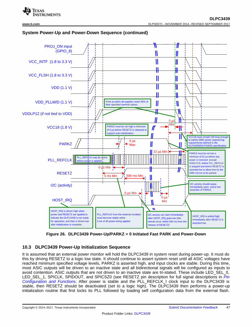
500 ms Min
PLL_REFCLK may be active before power is applied.
HOST_IRQ is driven high when power and RESETZ are applied to indicate the DLPC3439 is not ready for operation, and then is driven low after initialization is complete.
0 µs Min
0 µs Max
PARKZ must be set low a minimum of 32 µs before any power is removed (except VDDLP12), before PLL_REFCLK is stopped and before RESETZ is asserted low to allow time for the DMD mirrors to be parked.
0 µs Min
5 ms Min
PLL_REFCLK from the external oscillator must become stable within5 ms of all power being applied
I2C access can start immediately after HOST_IRQ goes low (this should occur within 500 ms from the release of RESETZ)
HOST_IRQ is pulled high immediately after RESETZ is asserted low.
PARKZ
PLL_REFCLK
RESETZ
I2C (activity)
HOST_IRQ
VDD_PLLM/D (1.1 V)
VDD (1.1 V)
VCC18 (1.8 V)
VDDLP12 (if not tied to VDD)
Point at which all supplies reach 95% of their specified nominal values.
PARKZ must be set high a minimum of 0 µs before RESETZ is released to support auto-initialization.
PROJ_ON input (GPIO_8)
VCC_INTF (1.8 to 3.3 V)
VCC_FLSH (1.8 to 3.3 V)
I2C activity should cease immediately upon active low assertion of PARKZ.
0 µsMin
VCC18 must remain ON long enough to satisfy DMD power sequencing requirements defined in the DLPA3000/DLPA3005 specification.
32 µs Min
0 µsMin
47
DLPC3439www.ti.com DLPS057C –NOVEMBER 2014–REVISED SEPTEMBER 2017
Product Folder Links: DLPC3439
Submit Documentation FeedbackCopyright © 2014–2017, Texas Instruments Incorporated
System Power-Up and Power-Down Sequence (continued)
Figure 26. DLPC3439 Power-Up/PARKZ = 0 Initiated Fast PARK and Power-Down
10.3 DLPC3439 Power-Up Initialization SequenceIt is assumed that an external power monitor will hold the DLPC3439 in system reset during power-up. It must dothis by driving RESETZ to a logic low state. It should continue to assert system reset until all ASIC voltages havereached minimum specified voltage levels, PARKZ is asserted high, and input clocks are stable. During this time,most ASIC outputs will be driven to an inactive state and all bidirectional signals will be configured as inputs toavoid contention. ASIC outputs that are not driven to an inactive state are tri-stated. These include LED_SEL_0,LED_SEL_1, SPICLK, SPIDOUT, and SPICSZ0 (see RESETZ pin description for full signal descriptions in PinConfiguration and Functions. After power is stable and the PLL_REFCLK_I clock input to the DLPC3439 isstable, then RESETZ should be deactivated (set to a logic high). The DLPC3439 then performs a power-upinitialization routine that first locks its PLL followed by loading self configuration data from the external flash.

48
DLPC3439DLPS057C –NOVEMBER 2014–REVISED SEPTEMBER 2017 www.ti.com
Product Folder Links: DLPC3439
Submit Documentation Feedback Copyright © 2014–2017, Texas Instruments Incorporated
DLPC3439 Power-Up Initialization Sequence (continued)Upon release of RESETZ, all DLPC3439 I/Os will become active. Immediately following the release of RESETZ,the HOST_IRQ signal will be driven high to indicate that the auto initialization routine is in progress. However,since a pullup resistor is connected to signal HOST_IRQ, this signal will have already gone high before theDLPC3439 actively drives it high. Upon completion of the auto-initialization routine, the DLPC3439 will driveHOST_IRQ low to indicate the initialization done state of the DLPC3439 has been reached.
Note that the host processor can start sending I2C commands after HOST_IRQ goes low.
10.4 DMD Fast PARK Control (PARKZ)The PARKZ signal is defined to be an early warning signal that should alert the ASIC 32 µs before DC supplyvoltages have dropped below specifications in fast PARK operation. This allows the ASIC time to park the DMD,ensuring the integrity of future operation. Note that the reference clock should continue to run and RESETZshould remain deactivated for at least 32 µs after PARKZ has been deactivated (set to a logic low) to allow thepark operation to complete.
10.5 Hot Plug UsageThe DLPC3439 provides fail-safe I/O on all host interface signals (signals powered by VCC_INTF). This allowsthese inputs to be driven high even when no I/O power is applied. Under this condition, the DLPC3439 will notload the input signal nor draw excessive current that could degrade ASIC reliability. For example, the I2C busfrom the host to other components would not be affected by powering off VCC_INTF to the DLPC3439. TIrecommends weak pullups or pulldowns on signals feeding back to the host to avoid floating inputs.
If the I/O supply (VCC_INTF) is powered off, but the core supply (VDD) is powered on, then the corresponding inputbuffer may experience added leakage current, but this does not damage the DLPC3439.
10.6 Maximum Signal Transition TimeUnless otherwise noted, 10 ns is the maximum recommended 20 to 80% rise or fall time to avoid input bufferoscillation. This applies to all DLPC3439 input signals. However, the PARKZ input signal includes an additionalsmall digital filter that ignores any input buffer transitions caused by a slower rise or fall time for up to 150 ns.
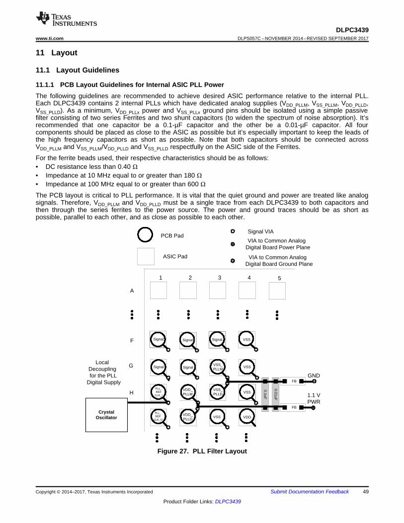
VSS
VDD
VSS_PLLD
VDD_PLLD
0.1uF
VSS
VSS_PLLMSignal
VSS
F
H
A
32
VDD
PLL_REF
CLK_I
Signal
4
VDD_PLLM
1
Signal VSS
5
VIA to Common AnalogDigital Board Power Plane
VIA to Common AnalogDigital Board Ground Plane
ASIC Pad
PCB Pad
Local Decoupling for the PLL
Digital Supply
Signal VIA
FB
SignalSignal
PLL_REF
CLK_O
FB
0.01uF
Crystal Oscillator
1.1 VPWR
GND
G
49
DLPC3439www.ti.com DLPS057C –NOVEMBER 2014–REVISED SEPTEMBER 2017
Product Folder Links: DLPC3439
Submit Documentation FeedbackCopyright © 2014–2017, Texas Instruments Incorporated
11 Layout
11.1 Layout Guidelines
11.1.1 PCB Layout Guidelines for Internal ASIC PLL PowerThe following guidelines are recommended to achieve desired ASIC performance relative to the internal PLL.Each DLPC3439 contains 2 internal PLLs which have dedicated analog supplies (VDD_PLLM, VSS_PLLM, VDD_PLLD,VSS_PLLD). As a minimum, VDD_PLLx power and VSS_PLLx ground pins should be isolated using a simple passivefilter consisting of two series Ferrites and two shunt capacitors (to widen the spectrum of noise absorption). It’srecommended that one capacitor be a 0.1-µF capacitor and the other be a 0.01-µF capacitor. All fourcomponents should be placed as close to the ASIC as possible but it’s especially important to keep the leads ofthe high frequency capacitors as short as possible. Note that both capacitors should be connected acrossVDD_PLLM and VSS_PLLM/VDD_PLLD and VSS_PLLD respectfully on the ASIC side of the Ferrites.
For the ferrite beads used, their respective characteristics should be as follows:• DC resistance less than 0.40 Ω• Impedance at 10 MHz equal to or greater than 180 Ω• Impedance at 100 MHz equal to or greater than 600 Ω
The PCB layout is critical to PLL performance. It is vital that the quiet ground and power are treated like analogsignals. Therefore, VDD_PLLM and VDD_PLLD must be a single trace from each DLPC3439 to both capacitors andthen through the series ferrites to the power source. The power and ground traces should be as short aspossible, parallel to each other, and as close as possible to each other.
Figure 27. PLL Filter Layout

50
DLPC3439DLPS057C –NOVEMBER 2014–REVISED SEPTEMBER 2017 www.ti.com
Product Folder Links: DLPC3439
Submit Documentation Feedback Copyright © 2014–2017, Texas Instruments Incorporated
Layout Guidelines (continued)11.1.2 DLPC3439 Reference ClockThe DLPC3439 requires an external reference clock to feed its internal PLL. A crystal oscillator can supply thisreference. For flexibility, the DLPC3439 accepts either of two reference clock frequencies, but both must have amaximum frequency variation of ±200 ppm (including aging, temperature, and trim component variation).
The two DLPC3439 devices require a single dedicated oscillator where the oscillator output drives bothDLPC3439 devices. The oscillator must drive the PLL_REFCLK_I pin on each DLPC3439 and thePLL_REFCLK_O pins should be left unconnected.
The external oscillator must be able to drive at least a 15-pF load. Routing length from the oscillator to eachDLPC3439 should be closely matched.
11.1.3 General PCB RecommendationsTI recommends 1-oz. copper planes in the PCB design to achieve needed thermal connectivity.
11.1.4 General Handling Guidelines for Unused CMOS-Type PinsTo avoid potentially damaging current caused by floating CMOS input-only pins, TI recommends that unusedASIC input pins be tied through a pullup resistor to its associated power supply or a pulldown to ground. ForASIC inputs with an internal pullup or pulldown resistors, it is unnecessary to add an external pullup or pulldownunless specifically recommended. Note that internal pullup and pulldown resistors are weak and should not beexpected to drive the external line. The DLPC3439 implements very few internal resistors and these are noted inthe pin list. When external pullup or pulldown resistors are needed for pins that have built-in weak pullups orpulldowns, use the value 8 kΩ (max).
Unused output-only pins should never be tied directly to power or ground, but can be left open.
When possible, TI recommends that unused bidirectional I/O pins be configured to their output state such thatthe pin can be left open. If this control is not available and the pins may become an input, then they should bepulled-up (or pulled-down) using an appropriate, dedicated resistor.

51
DLPC3439www.ti.com DLPS057C –NOVEMBER 2014–REVISED SEPTEMBER 2017
Product Folder Links: DLPC3439
Submit Documentation FeedbackCopyright © 2014–2017, Texas Instruments Incorporated
Layout Guidelines (continued)
(1) Maximum signal routing length includes escape routing.(2) Multi-board DMD routing length is more restricted due to the impact of the connector.(3) Due to board variations, these are impossible to define. Any board designs should SPICE simulate with the ASIC IBIS models to ensure
single routing lengths do not exceed requirements.
11.1.5 Maximum Pin-to-Pin, PCB Interconnects Etch Lengths
Table 11. Max Pin-to-Pin PCB Interconnect Recommendations (1) (2)
DMD BUS SIGNALSIGNAL INTERCONNECT TOPOLOGY
UNITSINGLE BOARD SIGNAL ROUTINGLENGTH
MULTI-BOARD SIGNAL ROUTINGLENGTH
DMD_HS_CLK_PDMD_HS_CLK_N
6.0152.4 See (3) inch
(mm)DMD_HS_WDATA_A_PDMD_HS_WDATA_A_N
6.0152.4 See (3) inch
(mm)
DMD_HS_WDATA_B_PDMD_HS_WDATA_B_NDMD_HS_WDATA_C_PDMD_HS_WDATA_C_NDMD_HS_WDATA_D_PDMD_HS_WDATA_D_NDMD_HS_WDATA_E_PDMD_HS_WDATA_E_NDMD_HS_WDATA_F_PDMD_HS_WDATA_F_NDMD_HS_WDATA_G_PDMD_HS_WDATA_G_NDMD_HS_WDATA_H_PDMD_HS_WDATA_H_N
DMD_LS_CLK 6.5165.1 See (3) inch
(mm)
DMD_LS_WDATA 6.5165.1 See (3) inch
(mm)
DMD_LS_RDATA 6.5165.1 See (3) inch
(mm)
DMD_DEN_ARSTZ 7.0177.8 See (3) inch
(mm)
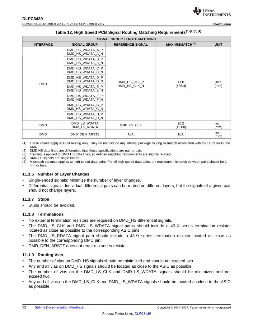
52
DLPC3439DLPS057C –NOVEMBER 2014–REVISED SEPTEMBER 2017 www.ti.com
Product Folder Links: DLPC3439
Submit Documentation Feedback Copyright © 2014–2017, Texas Instruments Incorporated
(1) These values apply to PCB routing only. They do not include any internal package routing mismatch associated with the DLPC3439, theDMD.
(2) DMD HS data lines are differential, thus these specifications are pair-to-pair.(3) Training is applied to DMD HS data lines, so defined matching requirements are slightly relaxed.(4) DMD LS signals are single ended.(5) Mismatch variance applies to high-speed data pairs. For all high-speed data pairs, the maximum mismatch between pairs should be 1
mm or less.
Table 12. High Speed PCB Signal Routing Matching Requirements (1) (2) (3) (4)
SIGNAL GROUP LENGTH MATCHINGINTERFACE SIGNAL GROUP REFERENCE SIGNAL MAX MISMATCH (5) UNIT
DMD
DMD_HS_WDATA_A_PDMD_HS_WDATA_A_N
DMD_HS_CLK_PDMD_HS_CLK_N
±1.0(±25.4)
inch(mm)
DMD_HS_WDATA_B_PDMD_HS_WDATA_B_NDMD_HS_WDATA_C_PDMD_HS_WDATA_C_NDMD_HS_WDATA_D_PDMD_HS_WDATA_D_NDMD_HS_WDATA_E_PDMD_HS_WDATA_E_NDMD_HS_WDATA_F_PDMD_HS_WDATA_F_NDMD_HS_WDATA_G_PDMD_HS_WDATA_G_NDMD_HS_WDATA_H_PDMD_HS_WDATA_H_N
DMD DMD_LS_WDATADMD_LS_RDATA DMD_LS_CLK ±0.2
(±5.08)inch(mm)
DMD DMD_DEN_ARSTZ N/A N/A inch(mm)
11.1.6 Number of Layer Changes• Single-ended signals: Minimize the number of layer changes.• Differential signals: Individual differential pairs can be routed on different layers, but the signals of a given pair
should not change layers.
11.1.7 Stubs• Stubs should be avoided.
11.1.8 Terminations• No external termination resistors are required on DMD_HS differential signals.• The DMD_LS_CLK and DMD_LS_WDATA signal paths should include a 43-Ω series termination resistor
located as close as possible to the corresponding ASIC pins.• The DMD_LS_RDATA signal path should include a 43-Ω series termination resistor located as close as
possible to the corresponding DMD pin.• DMD_DEN_ARSTZ does not require a series resistor.
11.1.9 Routing Vias• The number of vias on DMD_HS signals should be minimized and should not exceed two.• Any and all vias on DMD_HS signals should be located as close to the ASIC as possible.• The number of vias on the DMD_LS_CLK and DMD_LS_WDATA signals should be minimized and not
exceed two.• Any and all vias on the DMD_LS_CLK and DMD_LS_WDATA signals should be located as close to the ASIC
as possible.

53
DLPC3439www.ti.com DLPS057C –NOVEMBER 2014–REVISED SEPTEMBER 2017
Product Folder Links: DLPC3439
Submit Documentation FeedbackCopyright © 2014–2017, Texas Instruments Incorporated
11.2 Layout Example
Figure 28. Board Layout
11.3 Thermal ConsiderationsThe underlying thermal limitation for the DLPC3439 is that the maximum operating junction temperature (TJ)cannot be exceeded (this is defined in the Recommended Operating Conditions). This temperature is dependenton operating ambient temperature, airflow, PCB design (including the component layout density and the amountof copper used), power dissipation of the DLPC3439, and power dissipation of surrounding components. TheDLPC3439’s package is designed primarily to extract heat through the power and ground planes of the PCB.Thus, copper content and airflow over the PCB are important factors.
The recommended maximum operating ambient temperature (TA) is provided primarily as a design target and isbased on maximum DLPC3439 power dissipation and RθJA at 0 m/s of forced airflow, where RθJA is the thermalresistance of the package as measured using a glater test PCB with two, 1-oz power planes. This JEDEC testPCB is not necessarily representative of the DLPC3439 PCB; the reported thermal resistance may not beaccurate in the actual product application. Although the actual thermal resistance may be different, it is the bestinformation available during the design phase to estimate thermal performance. However, after the PCB isdesigned and the product is built, TI highly recommends that thermal performance is measured and validated.

54
DLPC3439DLPS057C –NOVEMBER 2014–REVISED SEPTEMBER 2017 www.ti.com
Product Folder Links: DLPC3439
Submit Documentation Feedback Copyright © 2014–2017, Texas Instruments Incorporated
Thermal Considerations (continued)To do this, measure the top center case temperature under the worse case product scenario (maximum powerdissipation, maximum voltage, maximum ambient temperature) and validated not to exceed the maximumrecommended case temperature (TC). This specification is based on the measured φJT for the DLPC3439package and provides a relatively accurate correlation to junction temperature. Take care when measuring thiscase temperature to prevent accidental cooling of the package surface. TI recommends a small (approximately40 gauge) thermocouple. The bead and thermocouple wire should contact the top of the package and becovered with a minimal amount of thermally conductive epoxy. The wires should be routed closely along thepackage and the board surface to avoid cooling the bead through the wires.

55
DLPC3439www.ti.com DLPS057C –NOVEMBER 2014–REVISED SEPTEMBER 2017
Product Folder Links: DLPC3439
Submit Documentation FeedbackCopyright © 2014–2017, Texas Instruments Incorporated
12 Device and Documentation Support
12.1 Device Support
12.1.1 Third-Party Products DisclaimerTI'S PUBLICATION OF INFORMATION REGARDING THIRD-PARTY PRODUCTS OR SERVICES DOES NOTCONSTITUTE AN ENDORSEMENT REGARDING THE SUITABILITY OF SUCH PRODUCTS OR SERVICESOR A WARRANTY, REPRESENTATION OR ENDORSEMENT OF SUCH PRODUCTS OR SERVICES, EITHERALONE OR IN COMBINATION WITH ANY TI PRODUCT OR SERVICE.
12.1.2 Device Nomenclature
12.1.2.1 Device Markings
Marking Definitions:
Line 1: DLP® Device Name: DLPC343x = x indicates a 9 device name ID.SC: Solder ball composition
e1: Indicates lead-free solder balls consisting of SnAgCu.G8: Indicates lead-free solder balls consisting of tin-silver-copper (SnAgCu) with silver content.less than or equal to 1.5% and that the mold compound meets TI's definition of green.
Line 2: TI Part NumberDLP® Device Name: DLPC343x = x indicates a 9 device name ID.R corresponds to the TI device revision letter for example A, B or C.XXX corresponds to the device package designator.
Line 3: XXXXXXXXXX-TT Manufacturer Part NumberLine 4: LLLLLL.ZZZ Foundry lot code for semiconductor wafers
LLLLLL: Fab lot numberZZZ: Lot split number
Line 5: XX YYWW ES: Package assembly informationXX: Manufacturing siteYYWW: Date code (YY = Year, WW = Week)

Vertical Back Porch (VBP)
Vertical Front Porch (VFP)
HorizontalBackPorch(HBP)
HorizontalFrontPorch(HFP)
TLPF
TPPL
APPL
ALPF
56
DLPC3439DLPS057C –NOVEMBER 2014–REVISED SEPTEMBER 2017 www.ti.com
Product Folder Links: DLPC3439
Submit Documentation Feedback Copyright © 2014–2017, Texas Instruments Incorporated
Device Support (continued)
NOTE1. Engineering prototype samples are marked with an X suffix appended to the TI part
number. For example, 2512737-0001X.2. See Input Source - Frame Rates for DLPC3439 resolutions on the DMD supported per
part number.
12.1.3 Video Timing Parameter DefinitionsActive Lines Per Frame (ALPF) Defines the number of lines in a frame containing displayable data: ALPF is a
subset of the TLPF.
Active Pixels Per Line (APPL) Defines the number of pixel clocks in a line containing displayable data: APPLis a subset of the TPPL.
Horizontal Back Porch (HBP) Blanking Number of blank pixel clocks after horizontal sync but before0 the firstactive pixel. Note: HBP times are references to the leading (active) edge of the respective syncsignal.
Horizontal Front Porch (HFP) Blanking Number of blank pixel clocks after the last active pixel but beforeHorizontal Sync.
Horizontal Sync (HS) Timing reference point that defines the start of each horizontal interval (line). Theabsolute reference point is defined by the active edge of the HS signal. The active edge (eitherrising or falling edge as defined by the source) is the reference from which all horizontal blankingparameters are measured.
Total Lines Per Frame (TLPF) Defines the vertical period (or frame time) in lines: TLPF = Total number of linesper frame (active and inactive).
Total Pixel Per Line (TPPL) Defines the horizontal line period in pixel clocks: TPPL = Total number of pixelclocks per line (active and inactive).
Vertical Sync (VS) Timing reference point that defines the start of the vertical interval (frame). The absolutereference point is defined by the active edge of the VS signal. The active edge (either rising orfalling edge as defined by the source) is the reference from which all vertical blanking parametersare measured.
Vertical Back Porch (VBP) Blanking Number of blank lines after the leading edge of vertical sync but beforethe first active line.
Vertical Front Porch (VFP) Blanking Number of blank lines after the last active line but before the leadingedge of vertical sync.
Figure 29. Timing Parameter Diagram

57
DLPC3439www.ti.com DLPS057C –NOVEMBER 2014–REVISED SEPTEMBER 2017
Product Folder Links: DLPC3439
Submit Documentation FeedbackCopyright © 2014–2017, Texas Instruments Incorporated
12.2 Related LinksThe table below lists quick access links. Categories include technical documents, support and communityresources, tools and software, and quick access to sample or buy.
Table 13. Related Links
PARTS PRODUCT FOLDER SAMPLE & BUY TECHNICALDOCUMENTS
TOOLS &SOFTWARE
SUPPORT &COMMUNITY
DLPC3439 Click here Click here Click here Click here Click hereDLP4710 Click here Click here Click here Click here Click here
DLPA3005 Click here Click here Click here Click here Click hereDLPA3000 Click here Click here Click here Click here Click here
12.3 Community ResourcesThe following links connect to TI community resources. Linked contents are provided "AS IS" by the respectivecontributors. They do not constitute TI specifications and do not necessarily reflect TI's views; see TI's Terms ofUse.
TI E2E™ Online Community TI's Engineer-to-Engineer (E2E) Community. Created to foster collaborationamong engineers. At e2e.ti.com, you can ask questions, share knowledge, explore ideas and helpsolve problems with fellow engineers.
Design Support TI's Design Support Quickly find helpful E2E forums along with design support tools andcontact information for technical support.
12.4 TrademarksIntelliBright, E2E are trademarks of Texas Instruments.All other trademarks are the property of their respective owners.
12.5 Electrostatic Discharge CautionThese devices have limited built-in ESD protection. The leads should be shorted together or the device placed in conductive foamduring storage or handling to prevent electrostatic damage to the MOS gates.
12.6 GlossarySLYZ022 — TI Glossary.
This glossary lists and explains terms, acronyms, and definitions.
13 Mechanical, Packaging, and Orderable InformationThe following pages include mechanical, packaging, and orderable information. This information is the mostcurrent data available for the designated devices. This data is subject to change without notice and revision ofthis document. For browser-based versions of this data sheet, refer to the left-hand navigation.

DLPC3439DLPS057C –NOVEMBER 2014–REVISED SEPTEMBER 2017 www.ti.com
58
Product Folder Links: DLPC3439
Submit Documentation Feedback Copyright © 2014–2017, Texas Instruments Incorporated
(1) The marketing status values are defined as follows:ACTIVE: Product device recommended for new designs.LIFEBUY: TI has announced that the device will be discontinued, and a lifetime-buy period is in effect.NRND: Not recommended for new designs. Device is in production to support existing customers, but TI does not recommend using this part in a new design.PRE_PROD Unannounced device, not in production, not available for mass market, nor on the web, samples not available.PREVIEW: Device has been announced but is not in production. Samples may or may not be available.OBSOLETE: TI has discontinued the production of the device.space
(2) Eco Plan - The planned eco-friendly classification: Pb-Free (RoHS), Pb-Free (RoHS Exempt), or Green (RoHS & no Sb/Br) - please check http://www.ti.com/productcontent for the latestavailability information and additional product content details.TBD: The Pb-Free/Green conversion plan has not been defined.Pb-Free (RoHS): TI's terms "Lead-Free" or "Pb-Free" mean semiconductor products that are compatible with the current RoHS requirements for all 6 substances, including therequirement that lead not exceed 0.1% by weight in homogeneous materials. Where designed to be soldered at high temperatures, TI Pb-Free products are suitable for use in specifiedlead-free processes.Pb-Free (RoHS Exempt): This component has a RoHS exemption for either 1) lead-based flip-chip solder bumps used between the die and package, or 2) lead-based die adhesive usedbetween the die and leadframe. The component is otherwise considered Pb-Free (RoHS compatible) as defined above.Green (RoHS & no Sb/Br): TI defines "Green" to mean Pb-Free (RoHS compatible), and free of Bromine (Br) and Antimony (Sb) based flame retardants (Br or Sb do not exceed 0.1% byweight in homogeneous material)space
(3) MSL, Peak Temp. -- The Moisture Sensitivity Level rating according to the JEDEC industry standard classifications, and peak solder temperature.space
(4) There may be additional marking, which relates to the logo, the lot trace code information, or the environmental category on the devicespace
(5) Multiple Device markings will be inside parentheses. Only on Device Marking contained in parentheses and separated by a "~" will appear on a device. If a line is indented then it is acontinuation of the previous line and the two combined represent the entire Device Marking for that device.
Important Information and Disclaimer: The information provided on this page represents TI's knowledge and belief as of the date that it is provided. TI bases its knowledge and beliefon information provided by third parties, and makes no representation or warranty as to the accuracy of such information. Efforts are underway to better integrate information from thirdparties. TI has taken and continues to take reasonable steps to provide representative and accurate information but may not have conducted destructive testing or chemical analysis onincoming materials and chemicals. TI and TI suppliers consider certain information to be proprietary, and thus CAS numbers and other limited information may not be available forrelease.In no event shall TI's liability arising out of such information exceed the total purchase price of the TI part(s) at issue in this document sold by TI to Customer on an annual basis.
13.1 Package Option Addendum
13.1.1 Packaging Information
Orderable Device Status (1) PackageType
PackageDrawing Pins Package
Qty Eco Plan (2) Lead/Ball Finish MSL Peak Temp (3) Op Temp (°C) Device Marking (4) (5)
DLPC3439CZEZ ACTIVE NFBGA ZEZ 201 160 Call TI Call TI Level-3-260C-168 HRS –30 to 85

www.ti.com
PACKAGE OUTLINE
C
A 13.112.9 B
13.112.9
1 MAX
TYP0.310.21
11.2TYP
11.2 TYP
0.8 TYP
0.8 TYP
201X 0.40.3
(0.9) TYP
(0.9) TYP
NFBGA - 1 mm max heightZEZ0201APLASTIC BALL GRID ARRAY
4221521/A 03/2015
NOTES: 1. All linear dimensions are in millimeters. Any dimensions in parenthesis are for reference only. Dimensioning and tolerancing per ASME Y14.5M. 2. This drawing is subject to change without notice.
BALL A1 CORNER
SEATING PLANE
BALL TYP 0.1 C
0.15 C A B0.08 C
SYMM
SYMM
BALL A1 CORNER
R
CDEFGHJKLMNP
1 2 3 4 5 6 7 8 9 10 11AB
12 13 14 15
SCALE 1.000

www.ti.com
EXAMPLE BOARD LAYOUT
201X ( )0.4(0.8) TYP
(0.8) TYP
( )METAL
0.40.05 MAX
SOLDER MASKOPENING
METAL UNDERSOLDER MASK
( )SOLDER MASKOPENING
0.4
0.05 MIN
NFBGA - 1 mm max heightZEZ0201APLASTIC BALL GRID ARRAY
4221521/A 03/2015
NOTES: (continued) 3. Final dimensions may vary due to manufacturing tolerance considerations and also routing constraints. For information, see Texas Instruments literature number SPRAA99 (www.ti.com/lit/spraa99).
SYMM
SYMM
LAND PATTERN EXAMPLESCALE:8X
1 2 3 4 5 6 7 8 9 10 11
B
A
C
D
E
F
G
H
J
K
L
M
N
P
R
12 13 14 15
NON-SOLDER MASKDEFINED
(PREFERRED)
SOLDER MASK DETAILSNOT TO SCALE
SOLDER MASKDEFINED

www.ti.com
EXAMPLE STENCIL DESIGN
(0.8) TYP
(0.8) TYP( ) TYP0.4
NFBGA - 1 mm max heightZEZ0201APLASTIC BALL GRID ARRAY
4221521/A 03/2015
NOTES: (continued) 4. Laser cutting apertures with trapezoidal walls and rounded corners may offer better paste release.
1 2 3 4 5 6 7 8 9 10 11
B
A
C
D
E
F
G
H
J
K
L
M
N
P
R
12 13 14 15
SYMM
SYMM
SOLDER PASTE EXAMPLEBASED ON 0.15 mm THICK STENCIL
SCALE:8X

IMPORTANT NOTICE
Texas Instruments Incorporated (TI) reserves the right to make corrections, enhancements, improvements and other changes to itssemiconductor products and services per JESD46, latest issue, and to discontinue any product or service per JESD48, latest issue. Buyersshould obtain the latest relevant information before placing orders and should verify that such information is current and complete.TI’s published terms of sale for semiconductor products (http://www.ti.com/sc/docs/stdterms.htm) apply to the sale of packaged integratedcircuit products that TI has qualified and released to market. Additional terms may apply to the use or sale of other types of TI products andservices.Reproduction of significant portions of TI information in TI data sheets is permissible only if reproduction is without alteration and isaccompanied by all associated warranties, conditions, limitations, and notices. TI is not responsible or liable for such reproduceddocumentation. Information of third parties may be subject to additional restrictions. Resale of TI products or services with statementsdifferent from or beyond the parameters stated by TI for that product or service voids all express and any implied warranties for theassociated TI product or service and is an unfair and deceptive business practice. TI is not responsible or liable for any such statements.Buyers and others who are developing systems that incorporate TI products (collectively, “Designers”) understand and agree that Designersremain responsible for using their independent analysis, evaluation and judgment in designing their applications and that Designers havefull and exclusive responsibility to assure the safety of Designers' applications and compliance of their applications (and of all TI productsused in or for Designers’ applications) with all applicable regulations, laws and other applicable requirements. Designer represents that, withrespect to their applications, Designer has all the necessary expertise to create and implement safeguards that (1) anticipate dangerousconsequences of failures, (2) monitor failures and their consequences, and (3) lessen the likelihood of failures that might cause harm andtake appropriate actions. Designer agrees that prior to using or distributing any applications that include TI products, Designer willthoroughly test such applications and the functionality of such TI products as used in such applications.TI’s provision of technical, application or other design advice, quality characterization, reliability data or other services or information,including, but not limited to, reference designs and materials relating to evaluation modules, (collectively, “TI Resources”) are intended toassist designers who are developing applications that incorporate TI products; by downloading, accessing or using TI Resources in anyway, Designer (individually or, if Designer is acting on behalf of a company, Designer’s company) agrees to use any particular TI Resourcesolely for this purpose and subject to the terms of this Notice.TI’s provision of TI Resources does not expand or otherwise alter TI’s applicable published warranties or warranty disclaimers for TIproducts, and no additional obligations or liabilities arise from TI providing such TI Resources. TI reserves the right to make corrections,enhancements, improvements and other changes to its TI Resources. TI has not conducted any testing other than that specificallydescribed in the published documentation for a particular TI Resource.Designer is authorized to use, copy and modify any individual TI Resource only in connection with the development of applications thatinclude the TI product(s) identified in such TI Resource. NO OTHER LICENSE, EXPRESS OR IMPLIED, BY ESTOPPEL OR OTHERWISETO ANY OTHER TI INTELLECTUAL PROPERTY RIGHT, AND NO LICENSE TO ANY TECHNOLOGY OR INTELLECTUAL PROPERTYRIGHT OF TI OR ANY THIRD PARTY IS GRANTED HEREIN, including but not limited to any patent right, copyright, mask work right, orother intellectual property right relating to any combination, machine, or process in which TI products or services are used. Informationregarding or referencing third-party products or services does not constitute a license to use such products or services, or a warranty orendorsement thereof. Use of TI Resources may require a license from a third party under the patents or other intellectual property of thethird party, or a license from TI under the patents or other intellectual property of TI.TI RESOURCES ARE PROVIDED “AS IS” AND WITH ALL FAULTS. TI DISCLAIMS ALL OTHER WARRANTIES ORREPRESENTATIONS, EXPRESS OR IMPLIED, REGARDING RESOURCES OR USE THEREOF, INCLUDING BUT NOT LIMITED TOACCURACY OR COMPLETENESS, TITLE, ANY EPIDEMIC FAILURE WARRANTY AND ANY IMPLIED WARRANTIES OFMERCHANTABILITY, FITNESS FOR A PARTICULAR PURPOSE, AND NON-INFRINGEMENT OF ANY THIRD PARTY INTELLECTUALPROPERTY RIGHTS. TI SHALL NOT BE LIABLE FOR AND SHALL NOT DEFEND OR INDEMNIFY DESIGNER AGAINST ANY CLAIM,INCLUDING BUT NOT LIMITED TO ANY INFRINGEMENT CLAIM THAT RELATES TO OR IS BASED ON ANY COMBINATION OFPRODUCTS EVEN IF DESCRIBED IN TI RESOURCES OR OTHERWISE. IN NO EVENT SHALL TI BE LIABLE FOR ANY ACTUAL,DIRECT, SPECIAL, COLLATERAL, INDIRECT, PUNITIVE, INCIDENTAL, CONSEQUENTIAL OR EXEMPLARY DAMAGES INCONNECTION WITH OR ARISING OUT OF TI RESOURCES OR USE THEREOF, AND REGARDLESS OF WHETHER TI HAS BEENADVISED OF THE POSSIBILITY OF SUCH DAMAGES.Unless TI has explicitly designated an individual product as meeting the requirements of a particular industry standard (e.g., ISO/TS 16949and ISO 26262), TI is not responsible for any failure to meet such industry standard requirements.Where TI specifically promotes products as facilitating functional safety or as compliant with industry functional safety standards, suchproducts are intended to help enable customers to design and create their own applications that meet applicable functional safety standardsand requirements. Using products in an application does not by itself establish any safety features in the application. Designers mustensure compliance with safety-related requirements and standards applicable to their applications. Designer may not use any TI products inlife-critical medical equipment unless authorized officers of the parties have executed a special contract specifically governing such use.Life-critical medical equipment is medical equipment where failure of such equipment would cause serious bodily injury or death (e.g., lifesupport, pacemakers, defibrillators, heart pumps, neurostimulators, and implantables). Such equipment includes, without limitation, allmedical devices identified by the U.S. Food and Drug Administration as Class III devices and equivalent classifications outside the U.S.TI may expressly designate certain products as completing a particular qualification (e.g., Q100, Military Grade, or Enhanced Product).Designers agree that it has the necessary expertise to select the product with the appropriate qualification designation for their applicationsand that proper product selection is at Designers’ own risk. Designers are solely responsible for compliance with all legal and regulatoryrequirements in connection with such selection.Designer will fully indemnify TI and its representatives against any damages, costs, losses, and/or liabilities arising out of Designer’s non-compliance with the terms and provisions of this Notice.
Mailing Address: Texas Instruments, Post Office Box 655303, Dallas, Texas 75265Copyright © 2018, Texas Instruments Incorporated