Digitally Assisted Wireless Transceivers and · PDF fileDigitally Assisted Wireless...
90
Symposia on VLSI Technology and Circuits Kenichi Okada Tokyo Institute of Technology Digitally Assisted Wireless Transceivers and Synthesizers
Transcript of Digitally Assisted Wireless Transceivers and · PDF fileDigitally Assisted Wireless...
Symposia on VLSI Technology and Circuits
Kenichi Okada
Tokyo Institute of Technology
Digitally Assisted Wireless
Transceivers and Synthesizers

Outline
Slide 1
•Analog to Digital
•Digitization of Wireless TRX
•Digital Assistance
•Wireless Transceiver
• Frequency Synthesizer
• Future Analog Design
•Synthesizable Analog

Analog to Digital
Slide 2
AnalogDigitalAnalog
Digitization
Digital
Digital Assistance
• Scalability
• Portability
• Robustness
• Less redundancy

Further Digitization
Slide 3
DigitalAnalog
Digitization
Massive Digital Assistance
• Scalability
• Portability
• Robustness
• Less redundancy
Digital
Digital

Case Study
Slide 4
Partially replaced by pure digital-domain “calculation”
(NOT time-domain analog processing)
• Filter: LPF in AD-PLL, LPF in wireless TX
• Equalizer: FIR in wireless, OFDM
• PLL: carrier and timing recovery in wireless RX
•Mixer: Low-IF transceiver
Only analog-domain
•Oscillator: Clock generation
•Data converter: V-to-D, D-to-V, D-to-I, C-to-D,..
•Analog amplifier: voltage-to-voltage
Diffic
ult fo
r dig
itizatio
n

History of Timing Recovery
*F. Gardner, IEEE Trans. Comm. 1993
Analog recovery
Digitally-assisted
analog recovery
Digital recovery
sampling clocktiming recovery
analog
processing
digital
processing
timing recovery
timing recovery
Slide 5
Analog Digital
analog
processing
digital
processing
analog
processing
digital
processing

Analog Demodulator
Slide 6
Costas-loop for BPSK
*H. Suzuki, et al., IEEE Trans. VT 1985
timing recovery loop (carrier & phase)
0/1
90o
0o
loop filter

Digital Carrier and Timing Recovery
Slide 7
NCO: Number-Controlled OscillatorLF: Loop FilterPD: Phase Detector
timing recovery (phase)
timing-recoveredsignal
PDLFNCO
carrier recovery (freq.)
rotationfilter
PDLFNCO
interpolationfilter
timing- & carrier-recovered signal
ADC
Everything is implemented in digital domain.
*F. Gardner, IEEE Trans. Comm. 1993

Recent Digital Transceiver
Slide 8
RXADC
ADC
TX
DAC
DAC
LPF
LPF
VGA
VGA
LPF
LPF
Analog Digital
RX
filter
TX
filter
Carrier
& Timing
Recovery
Dem
ap
per
FE
C
Deco
der
Map
per
FE
C
En
co
der
Zero-IF

Digital LPF in Wireless
Slide 9
RXADC
ADC
TX
DAC
DAC
LPF
LPF
VGA
VGA
LPF
LPF
Analog Digital
RX
filter
TX
filter
Carrier
& Timing
Recovery
Dem
ap
per
FE
C
Deco
der
Map
per
FE
C
En
co
der
LPF for transmitting bandwidth restriction

Digital Equalizers in Wireless
Slide 10
RXADC
ADC
TX
DAC
DAC
LPF
LPF
VGA
VGA
LPF
LPF
Analog Digital
RX
filter
TX
filter
Carrier
& Timing
Recovery
Dem
ap
per
FE
C
Deco
der
Map
per
FE
C
En
co
der
Adaptive RF&BB equalizer
RF&BB equalizer

Digitization of IF Mixer
Slide 11
Analog Digital
ADC
ADC
Analog Digital
ADC
Hetero-dyne RX
Low-IF RX
Very common for BT
1/f noise
Overhead for ADC
RF
RF IF
IF

Aim of This Talk
Slide 12
• Digitization
• Wireless transceiver is a good example of
digitized analog circuit. (for hinting)
• Toward “Synthesizable Analog Circuit”
• Digital assistance
• Digitally-designed analog
• Digital calibration/compensation is implemented
in a system level to satisfy complicated
requirements for wireless system.
• Mutual re-use of TX and RX for calibration

Outline
Slide 13
•Analog to Digital
•Digitization of Wireless TRX
•Digital Assistance
•Wireless Transceiver
• Frequency Synthesizer
• Future Analog Design
•Synthesizable Analog

Impairments in Wireless Transceiver
Slide 14
Mismatch in differential block
• DC offset in RX
• IIP2 in RX
• LO leakage in TX
Mismatch btw I and Q blocks
• Image signal
• Analog filter BW (LPF)
Non-linearity
• IMD in PA
*A. Jerng, “Digital Calibration for RF Transceivers,” ISSCC 2012, Tutorial 9
PVT variation
• Gain control
• Power control
• VCO LC tank
• ILFD/ILO
Environmental variation
• TX-to-RX distance
• Fading
• Antenna reflection

Digital Equalizers
Slide 15
RXADC
ADC
TX
DAC
DAC
LPF
LPF
VGA
VGA
LPF
LPF
Analog Digital
RX
filter
TX
filter
Carrier
& Timing
Recovery
Dem
ap
per
FE
C
Deco
der
Map
per
FE
C
En
co
der
Adaptive RF&BB equalizer
RF&BB equalizer
Environmental Variation
Fading by multi-path
flat or frequency selective

Automatic Gain Control (AGC)
Slide 16
RXADC
ADC
TX
DAC
DAC
LPF
LPF
VGA
VGA
LPF
LPF
Analog Digital
RX
filter
TX
filter
Carrier
& Timing
Recovery
Dem
ap
per
FE
C
Deco
der
Map
per
FE
C
En
co
der
Automatic Gain Control
DC offset cancel
Environmental Variation
Received signal strength
Antenna reflection

I/Q Mismatch
Slide 17
RX
ADC
ADC
TX
DAC
DAC
Digital
BB
LPF
LPF
VGA
VGA
LPF
LPF
Analog Digital
gain&phase
mismatch
phase mismatch
I
Q
I
Q

Image Rejection Ratio (IMRR)
Slide 18
LO leak
Desired
𝝎𝐋𝐎 −𝝎𝐁𝐁
[dB
m]
freq. [GHz]𝝎𝐋𝐎 +𝝎𝐁𝐁𝝎𝐋𝐎
IMRR [dB]
e.g. 𝝎𝐁𝐁 = 𝟏𝟎𝐌𝐇𝐳
Image

Image for Modulated Sig.
Slide 19
Image
Desired
𝝎𝐋𝐎 −𝝎𝐁𝐁
[dB
m]
freq. [GHz]𝝎𝐋𝐎 +𝝎𝐁𝐁𝝎𝐋𝐎
IMRR [dB]
I/Q mismatch degrades SNR.

Image Rejection Ratio (IMRR)
Slide 20
0
1
2
3
4
5
6
7
0 0.2 0.4 0.6 0.8 1
Ph
as
e E
rro
r [d
eg
]
Amplitude Error [dB]
Δg: Amplitude error ratio
Δθ: Phase error
Target:
0.2dB, 1.0degree
for IMRR of 35dB
𝑰𝑴𝑹𝑹 ≈𝜟𝒈𝟐 + 𝜟𝜽𝟐
𝟒

TX IMRR Calibration
Slide 21
I: 0o
Q: -90o
test signal
coupler
TX
Down-conversion is
required.
Detector can be used.
(2nd-order distortion)
IMLO
Desired
freq. [GHz]
𝝎𝐋𝐎 −𝝎𝐁𝐁 𝝎𝐋𝐎 +𝝎𝐁𝐁
𝝎𝐋𝐎

TX IMRR Calibration
Slide 22
I: 0o
Q: -90o
test signal
coupler
Detector
TX
IMLO
Desired
IMLO
Desired
𝝎𝐁𝐁
freq. [GHz]
𝟐𝝎𝐁𝐁0𝝎𝐋𝐎 −𝝎𝐁𝐁 𝝎𝐋𝐎 +𝝎𝐁𝐁
𝝎𝐋𝐎
freq. [GHz]
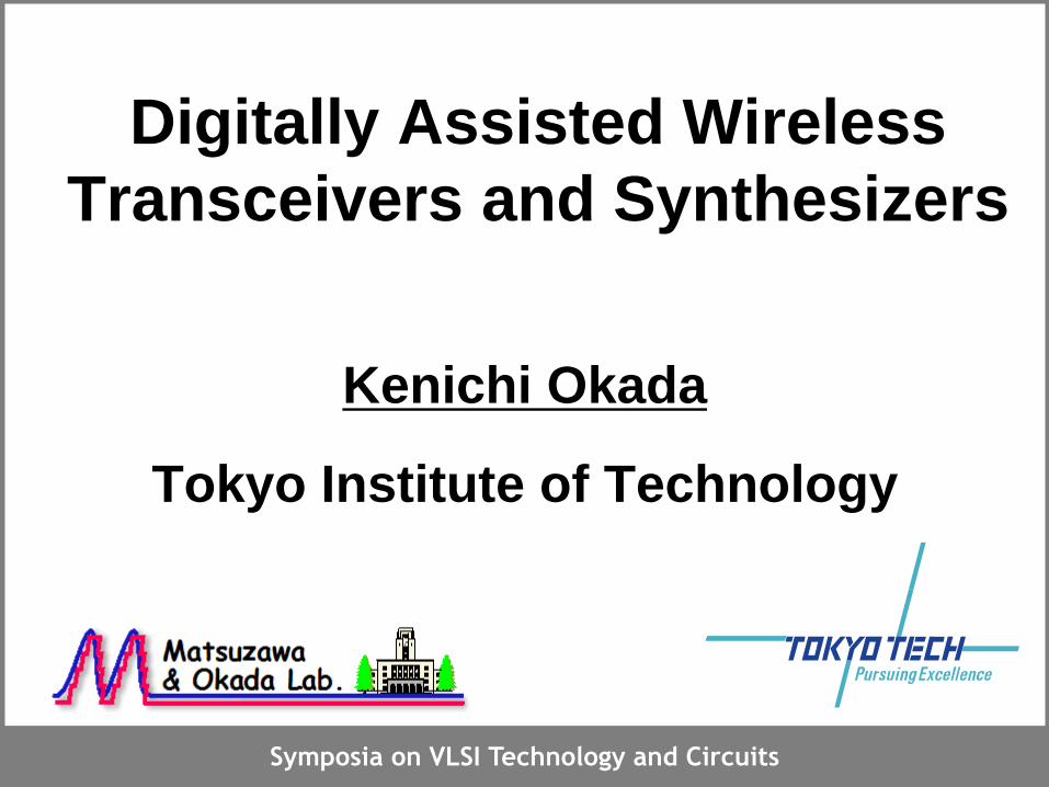
Detector
Slide 23
RF (e.g. 5GHz)
bias
LPF BB (e.g. 10MHz)
IMLO
Desired
IMLO
Desired
𝝎𝐁𝐁 𝟐𝝎𝐁𝐁0𝝎𝐋𝐎 −𝝎𝐁𝐁 𝝎𝐋𝐎 +𝝎𝐁𝐁
𝝎𝐋𝐎
𝒗𝐨𝐮𝐭 = 𝐋𝐏𝐅(𝑨 𝒗𝐢𝐧𝟐)

I/Q Mismatch Calibration by Loop-back
Slide 24
RX
ADC
ADC
TX
DAC
DAC
Digital
BB
LPF
LPF
VGA
VGA
LPF
LPF
coupler
Detector
TX
filter
• I/Q Amplitude offset
• I/Q Phase offset

I/Q Mismatch Calibration by Loop-back
Slide 25
RX
ADC
ADC
TX
DAC
DAC
LPF
LPF
VGA
VGA
LPF
LPF
coupler
Detector
TX
filter
• I/Q Amplitude offset
• I/Q Phase offset*Iason Vassiliou, et al., IEEE JSSC 2003.
Digital
BB
DFT

-20
-15
-10
-5
0
0.01 0.1 1 10 100
Frequency-Dependent I/Q Mismatch
Slide 26
TX DAC
DAC
LPF
LPF
Frequency [MHz]
Gain
[d
B]
I
Q
5% cut-off mismatch
causes a serious
frequency-dependent
I/Q mismatch.

-180
-150
-120
-90
-60
-30
0
0.01 0.1 1 10 100
-20
-15
-10
-5
0
0.01 0.1 1 10 100
Frequency-Dependent IMRR
Slide 27
Gain/phase mismatch can be frequency-dependent.
5% cut-off frequency mismatch
Freq. [MHz]
Freq. [MHz]
Gain
[d
B]
Ph
ase [
deg
.]
IMR
R [
dB
]
Freq. [MHz]
BW
-50
-40
-30
-20
0.01 0.1 1 10 100
1.5% (-42.5dB)
2.6% (-38.5dB)
-37dB@1MHz, -27dB@10MHz

Key Idea of Wireless Calibration
Slide 28
Self-calibration with less additional blocks
Reuse of TRX each other
TX = Signal Generator for RX calibration
RX = Spectrum Analyzer for TX calibration

Overall Procedure of TRX Calibration
Slide 29
1. RX BB LPF Calibration (using TX BB)• I/Q gain mismatch
• LPF cut-off mismatch (including VGA and ADC)
2. TX BB LPF Calibration (using RX BB)• I/Q gain mismatch
• LPF cut-off mismatch
3. TX I/Q Calibration (using detector and RX BB)• Impairments of mixer, LO, RF I/Q amps., etc
• compensated by digital BB
4. RX I/Q Calibration (using TX)• Impairments of mixer, LO, RF I/Q amps., etc
• compensated by digital BB

RX Filter Calibration (BB loopback)
Slide 30
RXADC
ADC
TX
DAC
DAC
Digital
BB
LPF
LPF
VGA LPF
LPF
Test-tone
generation
Gain/Phase
calculation
VGA and ADC are also included in RX BB calibration.
VGA
target

TX Filter Calibration (BB loopback)
Slide 31
RXADC
ADC
TX
DAC
DAC
Digital
BB
LPF
LPF
VGA LPF
LPF gain/cut-off mismatch between I/Q paths are calibrated.
VGA LPF
target
Test-tone
generation
Gain/Phase
calculation

target
RF Loop-Back Calibration for TX
Slide 32
RXADC
ADC
TX
DAC
DAC
LPF
LPF
VGA
VGA
LPF
LPF
Detector
*Iason Vassiliou, et al., IEEE JSSC 2003.
IM/LO
Calculation
by DFT
Test-to
ne
gen
era
tion
TX
filtercompensate
ADC is re-used for IM/LO calculation with DFT in BB.

target
RF Loop-Back Calibration for TX
Slide 33
RXADC
ADC
TX
DAC
DAC
LPF
LPF
VGA
VGA
LPF
LPF
Detector
*Iason Vassiliou, et al., IEEE JSSC 2003.
IM/LO
Calculation
by DFT
Test-to
ne
gen
era
tion
TX
filtercompensate
IMLO
Desired IMLO
Desired
freq. [GHz]
0
HPF

RF Loop-Back Calibration for RX
Slide 34
RXADC
ADC
TX
DAC
DAC
LPF
LPF
VGA
VGA
LPF
LPF
*Iason Vassiliou, et al., IEEE JSSC 2003.
I/Q mismatch
calculation
Test-to
ne
gen
era
tion
TX
filter
ATT
TX is used for a test-tone generator.
Desired
target

I/Q Gain/Phase Mismatch Calculation
Slide 35
t
t
*S. Lerstaveesin, et al., IEEE JSSC 2006.
𝐋𝐏𝐅 𝑰𝟐 −𝑸𝟐 ≅ 𝜟𝒈
𝐋𝐏𝐅 𝑰 ∗ 𝑸 ≅ −𝜟𝜽/𝟐
𝑰
𝑸
At least, a 10-bit ADC is required for a IMRR of 40dB.
𝐋𝐏𝐅 𝑰𝟐 +𝑸𝟐
RSSI AGC
Modulated signal can be used.
Background calibration

target
RF Loop-Back Calibration for RX
Slide 36
RXADC
ADC
TX
DAC
DAC
LPF
LPF
VGA
VGA
LPF
LPF
*Iason Vassiliou, et al., IEEE JSSC 2003.
Test-to
ne
gen
era
tion
TX
filter
ATT
I/Q mismatch
calculation
Desired
t
t

Calibration vs Compensation
Slide 37
Frequency independent (RF)
TX I/Q mismatch(RF) Digital compensation (BB TX filter)
RX I/Q mismatch(RF) Digital compensation (BB RX filter)
FDE/OFDM
Frequency independent (BB)
TX I/Q mismatch(BB) Digital compensation
RX I/Q mismatch(BB) Digitally-calibrated analog (AGC)
/ Digital compensation
Frequency dependent (BB)
TX I/Q mismatch(BB) Digitally-calibrated analog
RX I/Q mismatch(BB) Digitally-calibrated analog
/ Digital compensationas a typical case

60GHz Transceiver Calibration
Slide 38
RX
ADC
ADC
TX
DAC
DAC
LPF
LPF
VGA
VGA
LPF
LPF
DetectorDigital
BB
*T. Tsukizawa, et al., ISSCC 2013
5b 3.5GS/s
8b 1MS/s ADC
One additional ADC is used for a fine resolution.

Outline
Slide 39
•Analog to Digital
•Digitization of Wireless TRX
•Digital Assistance
•Wireless Transceiver
• Frequency Synthesizer
• Future Analog Design
•Synthesizable Analog

Calibration in Frequency Synthesizer
Slide 40
• AFC for capacitor-bank in LC-VCO
• ILFD/ILO Calibration
• Linearity calibration/compensation
− Loop-BW, Quantization noise, FM/Polar-TX
AFC: Automatic Frequency Calibration
ILFD: Injection-Locked Frequency Divider
ILO: Injection-Locked Oscillator (Multiplier)
VCO: frequency ← voltage (varactor, C-bank)
DCO: frequency ← code (C-bank, I-control)
TDC: code ← delay (PVT, noise, layout, etc)
(ADC: code ← voltage)
(DAC: voltage ← code)
(Amp: voltage ← voltage)

ILFD Calibration
Slide 41
Locked*/Free-run** frequency is used.
*S. Pellerano, et al., ISSCC 2008 **T. Shima, et al., APMC 2011
***W. Deng, et al., A-SSCC 2012
60GHz PLL

Summary of Transceiver Calibration
Slide 42
• Wireless transceiver is a big system.
• Historically, architecture-level digitization
has been applied with system-level
calibration and compensation for PVT
and environmental variations.
• Re-use of counter-part block for
calibration
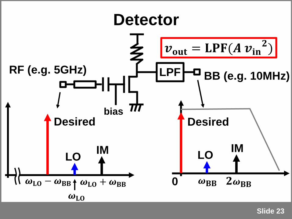
Outline
Slide 43
•Analog to Digital
•Digitization of Wireless TRX
•Digital Assistance
•Wireless Transceiver
• Frequency Synthesizer
• Future Analog Design
•Synthesizable Analog
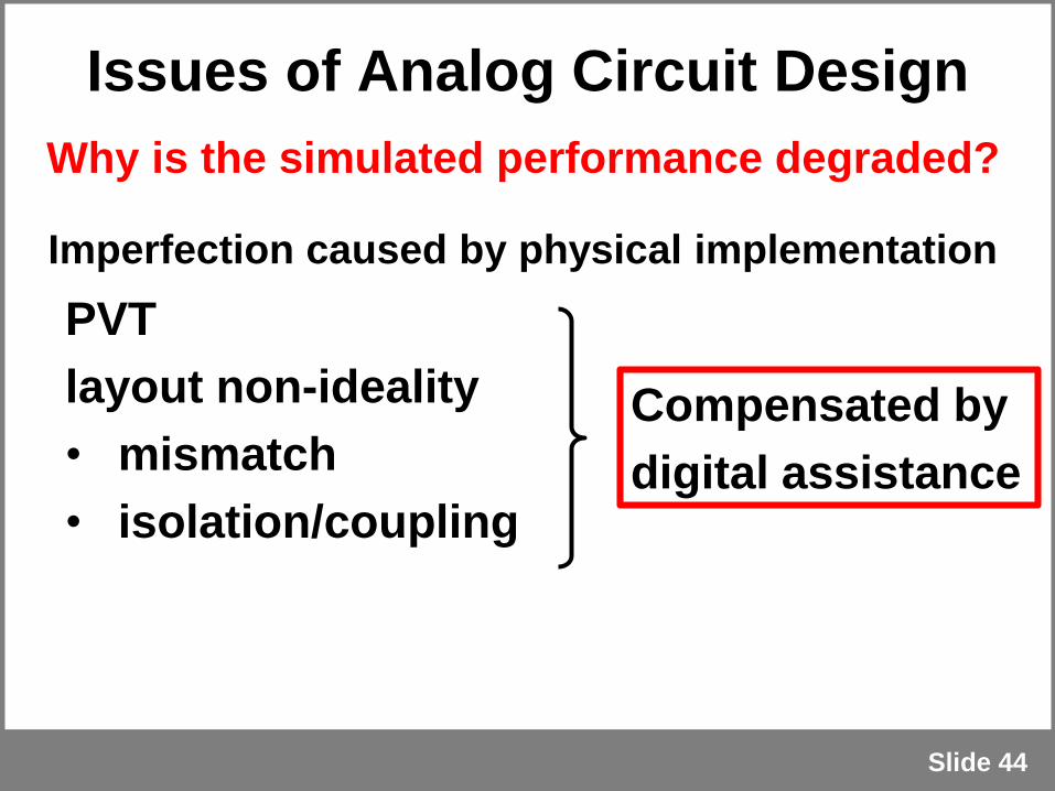
Issues of Analog Circuit Design
Slide 44
PVT
layout non-ideality
• mismatch
• isolation/coupling
Imperfection caused by physical implementation
Compensated by
digital assistance
Why is the simulated performance degraded?
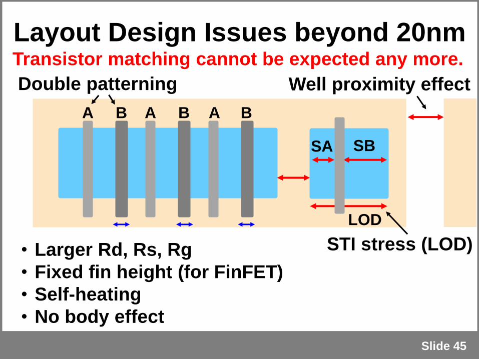
Layout Design Issues beyond 20nm
Slide 45
Double patterning
A A AB B B
STI stress (LOD)
SA SB
LOD
Well proximity effect
• Larger Rd, Rs, Rg
• Fixed fin height (for FinFET)
• Self-heating
• No body effect
Transistor matching cannot be expected any more.

Scaled CMOS Layout
Slide 46
65nm layout style 32nm layout style
• Uni-directional features
• Uniform gate dimension
• Gridded layout*M. Bohr, ISSCC 2009

Massive Digital Assistance
Slide 47
PVT
layout non-ideality
• mismatch
• isolation/coupling
Compensated by
digital assistance
Delay and linearity in delay can be calibrated
easily in time-domain analog circuits,
e.g. AD-PLL.

Further Analog Circuit
Slide 48
DigitalAnalog
Digitization
Massive Digital Assistance
• Scalability
• Portability
• Robustness
• Less redundancy
Digital
Digital

Outline
Slide 49
•Analog to Digital
•Digitization of Wireless TRX
•Digital Assistance
•Wireless Transceiver
• Frequency Synthesizer
• Future Analog Design
•Synthesizable Analog

Synthesizable Analog Circuits
Slide 50
GDSDigital design flow
Commercial P&R tools…
HDLmodule PLL
(CLK, …, OUT)
…
endmodule
with a standard-cell library
without any custom-designed cells
without manual placement

Analog Synthesis by Digital Tools
Slide 51
Verilog netlist
(gate-level)
Verilog
RTL
DCO
Logic
Logic
Logic Synt. Tool
GDSII
P&R Tool
Netlist
*W. Deng, et al., ISSCC 2014
Layout uncertainty
Pure digital
Digitally-designed Analog
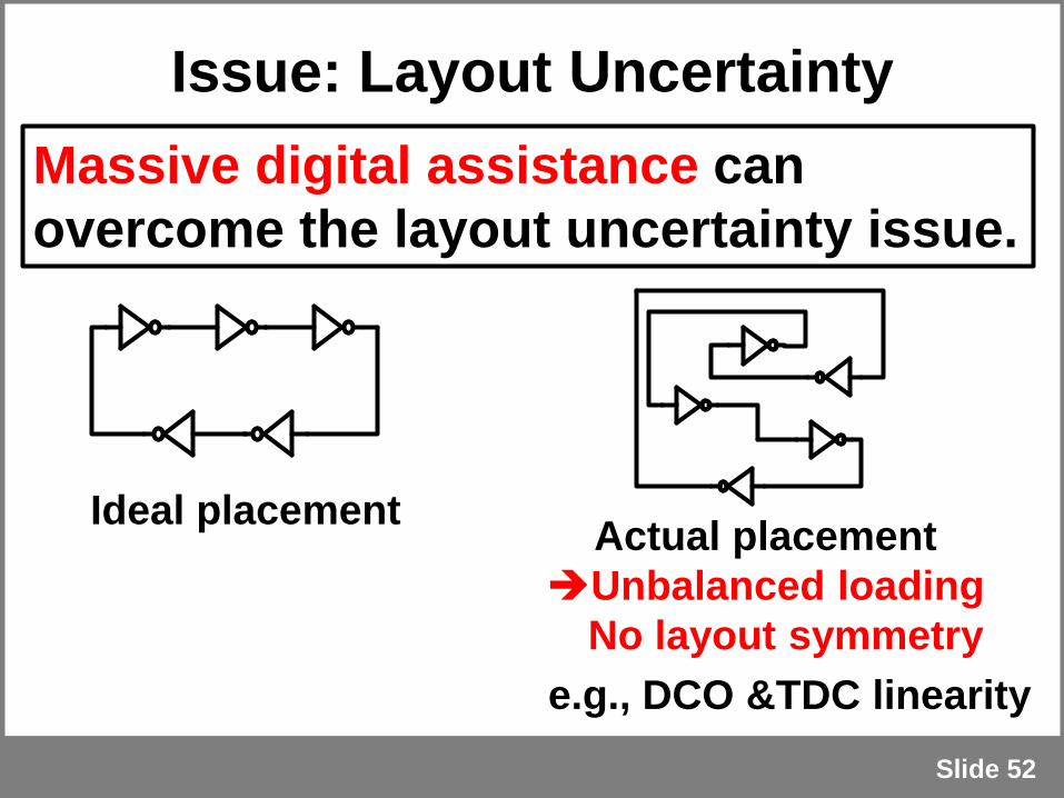
Issue: Layout Uncertainty
Slide 52
Ideal placementActual placement
Unbalanced loading
No layout symmetry
Massive digital assistance can
overcome the layout uncertainty issue.
e.g., DCO &TDC linearity

Synthesizable Analog Circuits
Slide 53
• Synthesizable PLL*
• Synthesizable DCO
• Synthesizable DAC
• Synthesizable TDC
• Synthesizable ADC**
*W. Deng, et al., ISSCC 2014 **S. Weaver, et al., IEEE TCAS-I 204
only by standard cells

Synthesizable ADC
Slide 54
*S. Weaver, et al., IEEE TCAS-I 2014
Comparator by NAND3
Gaussian offset distribution
ADC architecture
SNDR of 35.9dB, 210MS/s
Linearity compensation by inverse Gaussian
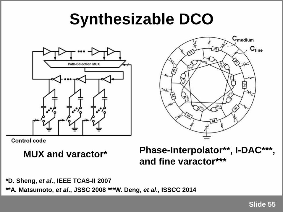
Synthesizable DCO
Slide 55
*D. Sheng, et al., IEEE TCAS-II 2007
**A. Matsumoto, et al., JSSC 2008 ***W. Deng, et al., ISSCC 2014
MUX and varactor* Phase-Interpolator**, I-DAC***,
and fine varactor***

Synthesizable DAC
Slide 56
Only standard cell
D0D1= 11 Vout= 0V
D0D1= 10 Vout= 0.5V
D0D1= 01 Vout= 0.5V
D0D1= 00 Vout= 1V
D0= 0 Vout= 1V
D0= 1 Vout= 0V

Synthesizable I-linear DAC
Slide 57
Only standard cell
D0
D1
D2
D3
1
1
Iout
×1
×2
×4
×8
*W. Deng, et al., ISSCC 2014
Current-starving RO
by NAND2

V-linear DAC vs I-linear DAC
Slide 58
0 4 8 12
Control Code
Cu
rren
t[m
A]
0.24
0.20
0.16
0.12
0 4 8 12
Control Code
Fre
qu
en
cy[G
Hz]
1.6
1.2
0.8
Current-starving RO
by NAND2

Stdcell Varactor
Slide 59
Vin
1.55ps@200MHz
*P. L. Chen, et al., TCAS II 2005

Performance Trade-off
Slide 60
Performance A
Pe
rfo
rman
ce B
Custom design
Custom design but easy
Synthesizable design

Performance Trade-off
Slide 61
Performance A
Pe
rfo
rman
ce B
Custom design
Custom design but easy
Synthesizable design
Synthesis-friendly architecture
A synthesis-friendly architecture
can improve performances.

Injection-Locked PLL (IL-PLL)
Slide 62
Conventional CP-PLL and TDC-PLL (AD-PLL)
• Phase lock: feedback
• Frequency lock: feedback
Injection-Locked PLL (IL-PLL)
• Phase lock: feed-forward
• Frequency lock: feedback
Injection-lock
Counter
*W. Deng, et al., ISSCC 2014
The fine timing feedback is not required.
Synthesis-friendly

Injection-Locked PLL
Slide 63
fref fout = N * fref
0.4*fref
Ph
as
e n
ois
e [
dB
c/H
z]
Offset Freq. [Hz]
PNVCO
PNref
+20log10(N)
Reference injection
*S. Ye, et al., IEEE JSSC 2002 **N. D. Dalt, IEEE TCAS-II 2014
Flicker of PNVCO
& Ref noise
Noise folding
& phase lock

Synthesizable IL-PLL
Slide 64
Frequency tracking with very narrow BW
*W. Deng, et al., ISSCC 2013 **A. Musa, et al., JSSC 2014 ***W. Deng, et al., ISSCC 2014
Phase lock
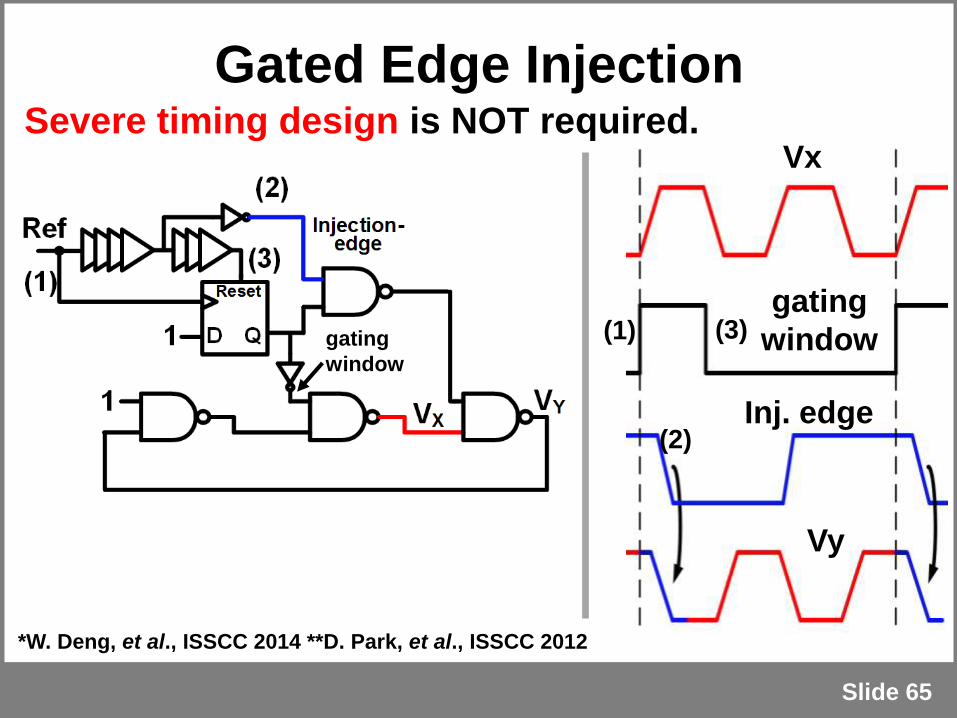
Gated Edge Injection
Slide 65
Vx
gating
window
Inj. edge
Vy
Severe timing design is NOT required.
(1)
(2)
(3)
*W. Deng, et al., ISSCC 2014 **D. Park, et al., ISSCC 2012
gating
window

Layout
Slide 66
CMOS 65nm
Area: 0.0066mm2
Jitter: 1.7ps
PDC: 780mW
FOM: -236.5 dB
60mm
110mm

Comparison of the state-of-the-art PLLs
Slide 67
*W. Deng, et al., ISSCC 2014

Comparison of Synthesizable PLL
Slide 68
This work
65nm
[22]
28nm
[23]
65nm
[24]
65nm
Power
[mW]0.78
@900MHz
13.7 @2.5GHz
3.1@250MHz
2.1@403MHz
Area
[mm2]0.0066 0.042 0.032 0.1
Integ.
Jitter [ps]1.7 N.A. 30 N.A.
RMS
Jitter [ps]2.8 3.2 N.A. 13.3
FOM [dB] -236.5 -218.6* -205.5 -214*W/ custom
cells?No No Yes Yes
Topology IL-base TDC-base TDC-base TDC-base*FOM is calculated based on RMS jitter.

Conclusion
Slide 69
• Digitization vs Digitally-Assisted Analog
• Digitally-Assisted Analog
to Digitally-Designed Analog
e.g. Synthesizable Analog Circuit
portability, scalability, robustness,..

References
Slide 70
[1] F. Gardner, "Interpolation in Digital Modems-Part I: Fundamentals," IEEE Trans. on
Communications, Vol. 41, No. 3, pp. 501-507, Mar. 1993.
[2] H. Suzuki, Y. Yamao, and H. Kikuchi, "A Single-Chip MSK Coherent Demodulator for
Mobile Radio Transmission," IEEE Trans. on Vecular Technology, Vol. VT-34, No. 4,
pp. 157-168, Nov. 1985.
[3] A. Jerng, “Digital Calibration for RF Transceivers,” ISSCC 2012, Tutorial 9.
[4] I. Vassiliou, et al., "A Digitally Calibrated 5.15-5.825GHz Transceiver for 802.11a
Wireless LANs in 0.18μm CMOS," IEEE Journal of Solid-State Circuits, Vol. 38, No. 12,
pp. 2221-2231, Dec. 2003.
[5] S. Lerstaveesin, et al., "A Complex Image Rejection Circuit with Sign Detection Only,"
IEEE Journal of Solid-State Circuits, Vol. 41, No. 12, pp. 2693-2702, Dec. 2006.
[6] T. Tsukizawa, et al., "A Fully Integrated 60GHz CMOS Transceiver Chipset Based on
WiGig/IEEE802.11ad with Built-in Self-Calibration for Mobile Applications," ISSCC Dig.
Tech. Papers, pp. 230-231, Feb. 2013.
[7] S. Pellerano, R. Mukhopadhyay, A. Ravi, J. Laskar, and Y. Palaskas, "A 39.1-to-
41.6GHz DS Fractional-N Frequency Synthesizer in 90nm CMOS," ISSCC Dig. Tech.
Papers, pp. 484-485, Feb. 2008.
[8] T. Shima, J. Sato, K. Mizuno, K. Takinami, "A 60 GHz CMOS PLL Synthesizer Using a
Wideband Injection-Locked Frequency Divider with Fast Calibration Technique,"
APMC, pp. 1530-1533, Dec. 2011.

References
Slide 71
[9] W. Deng, A. Musa, K. Okada, and A. Matsuzawa, "A 0.38mm2, 10MHz-6.6GHz
Quadrature Frequency Synthesizer Using Fractional-N Injection-Locked Technique,"
A-SSCC Dig. Tech. Papers, pp. 353-356, Nov. 2012.
[10] M. Bohr, "The New Era of Scaling in an SoC World," ISSCC Dig. Tech. Papers, pp.
23-28, Feb. 2009.
[11] W. Deng, A. Musa, T. Siriburanon, M. Miyahara, K. Okada, and A. Matsuzawa, "A
0.0066-mm2 780-μW Fully Synthesizable PLL with a Current Output DAC and an
Interpolative-Phase Coupled Oscillator using Edge Injection Technique," ISSCC Dig.
Tech. Papers, pp. 266-267, Feb. 2014.
[12] S. Weaver, B. Hershberg, and Un-Ku Moon, "Digitally Synthesized Stochastic Flash
ADC Using Only Standard Digital Cells," IEEE Transactions on Circuits and
Systems-I, Vol. 61, No. 1, pp. 84-91, Jan. 2014.
[13] P. M. Levine, and G. W. Roberts, “A High-Resolution Flash Time-to-Digital Converter
and Calibration Scheme,” IEEE International Test Conference, pp. 1148-1157, Oct.
2004.
[14] D. Sheng, et al., "An Ultra-Low-Power and Portable Digitally Controlled Oscillator for
SoC Applications," IEEE Trans. Circuits and Systems-II, Vol. 54, No. 11, pp. 954-958,
Nov. 2007.

References
Slide 72
[15] A. Matsumoto, S. Sakiyama, Y. Tokunaga, T. Morie, and S. Dosho, "A Design Method
and Developments of a Low-Power and High-Resolution Multiphase Generation
System," IEEE Journal of Solid-State Circuits, Vol. 43, No. 4, pp. 831-843, Apr. 2008.
[16] P. L. Chen, et al., "A Portable Digitally Controlled Oscillator Using Novel Varactors,"
IEEE Trans. Circuits and Systems-II, Vol. 52, No. 5, pp. 233-237, May 2007.
[17] S. Ye, L. Jansson, and I. Galton, "A Multiple-Crystal Interface PLL With VCO
Realignment to Reduce Phase Noise," IEEE Journal of Solid-State Circuits, Vol. 37,
No. 12, pp. 1795-1803, Dec. 2002.
[18] N. D. Dalt, "An Analysis of Phase Noise in Realigned VCOs," IEEE Transactions on
Circuits and Systems-II, Vol. 6, No. 3, pp. 143-147, March 2014.
[19] W. Deng, A. Musa, T. Siriburanon, M. Miyahara, K. Okada, and A. Matsuzawa, "A
0.022mm2 970μW Dual-Loop Injection-Locked PLL with -243dB FOM Using
Synthesizable All-Digital PVT Calibration Circuits," ISSCC Dig. Tech. Papers, pp.
248-249, Feb. 2013.
[20] A. Musa, W. Deng, T. Siriburanon, M. Miyahara, K. Okada, and A. Matsuzawa, "A
Compact, Low Power and Low Jitter Dual-Loop Injection Locked PLL Using All-
Digital PVT Calibration," IEEE Journal of Solid-State Circuits, Vol. 49, No. 1, pp. 50-
60, Jan. 2014.

References
Slide 73
[21] D. Park, and S. Cho, "A 14.2mW 2.55-to-3GHz Cascaded PLL with Reference
Injection, 800MHz Delta-Sigma modulator and 255fsrms Integrated Jitter in 0.13um
CMOS," ISSCC Dig. Tech. Papers, pp. 344-345, Feb. 2012.
[22] Y. Park, and D.D. Wentzloff, "An All-Digital PLL Synthesized from a Digital Standard
Cell Library in 65nm CMOS," IEEE Custom Integrated Circuits Conf., Oct. 2011.
[23] W. Kim, et al., "A 0.032mm2 3.1mW Synthesized Pixel Clock Generator with 30psrms
Integrated Jitter and 10-to-630MHz DCO Tuning Range," ISSCC Dig. Tech. Papers,
pp.250-251, Feb. 2013.
[24] M. Faisal, and D.D. Wentzloff, "An Automatically Placed-and-Routed ADPLL for the
MedRadio Band using PWM to Enhance DCO Resolution," IEEE Radio Frequency
Integrated Circuits Symposium, pp.115-118, Jun. 2013.
Other example:
[25] D. Kaczman, et al., "A Single-Chip 10-Band WCDMA/HSDPA 4-Band GSM/EDGE
SAW-less CMOS Receiver With DigRF 3G Interface and +90 dBm IIP2,“ IEEE JSSC,
Vol. 44, No. 3, pp. 718-739, March 2009.
Acknowledgement
Slide 74
This work was partially supported by MIC,
SCOPE, MEXT, STARC, and VDEC in
collaboration with Cadence Design
Systems, Inc., and Agilent Technologies
Japan, Ltd.

Appendix
Slide 75

𝐣
𝟏
𝟎
Up-conversion by cos(𝝎𝐋𝐎𝒕)
Slide 76
𝐜𝐨𝐬(𝝎𝐁𝐁𝒕) ∗ 𝐜𝐨𝐬(𝝎𝐋𝐎𝒕)
𝝎𝐋𝐎
−𝝎𝐋𝐎
∗ 𝐜𝐨𝐬 𝝎𝐋𝐎𝒕 =𝒆𝐣𝝎𝐋𝐎𝒕 + 𝒆−𝐣𝝎𝐋𝐎𝒕
𝟐𝒆−𝐣𝝎𝐋𝐎𝒕
𝟐
𝐜𝐨𝐬(𝝎𝐁𝐁𝒕) =𝒆𝐣𝝎𝐁𝐁𝒕 + 𝒆−𝐣𝝎𝐁𝐁𝒕
𝟐
𝝎𝐋𝐎 𝒆𝐣𝝎𝐋𝐎𝒕
𝟐
𝐣
𝟏
𝟎

Up-conversion by sin(𝝎𝐋𝐎𝒕)
Slide 77
𝐬𝐢𝐧(𝝎𝐁𝐁𝒕) ∗ 𝐬𝐢𝐧(𝝎𝐋𝐎𝒕)
𝝎𝐋𝐎
−𝝎𝐋𝐎
∗ 𝐬𝐢𝐧 𝝎𝐋𝐎𝒕 =−𝐣𝒆𝐣𝝎𝐋𝐎𝒕 + 𝐣𝒆−𝐣𝝎𝐋𝐎𝒕
𝟐𝐣𝒆−𝐣𝝎𝐋𝐎𝒕
𝟐
𝐬𝐢𝐧(𝝎𝐁𝐁𝒕) =−𝐣𝒆𝐣𝝎𝐁𝐁𝒕 + 𝐣𝒆−𝐣𝝎𝐁𝐁𝒕
𝟐
−𝐣𝒆𝐣𝝎𝐋𝐎𝒕
𝟐
𝝎𝐋𝐎
𝐣
𝟏
𝟎
𝐣
𝟏
𝟎

0
Ideal I/Q Up-Conversion
Slide 78
TX
-90o
I
0
0
0
0
Q
image
image
desired
desired
Image signals are canceled.

0
I/Q Up-Conversion with Mismatch
Slide 79
TX
-90o
I
00
0
Q
0
image
image
desired
desired
Image signals are NOT canceled.
+f

Calibration of Injection Lock Oscillator
Slide 80
*W. Deng, et al., A-SSCC 2012
PFD CP LPF Gating
Buffer
÷2Prog. Divider
÷32/÷33...÷126/÷127
÷2
÷3
÷4
÷5
÷2
÷3
÷4
4:1
Digital Logic
CLK
IN
4
10
7
3
7
7
16
Div. Chain...
÷2
8:1
÷2
Frac.
ILFD
÷10
10
3 3
4 Div. ChainDiv. ChainDiv. Chain
8:1
Quadrature
Output
4
DAC
MASH
1-1-1
Integ.
÷N
LFSR
Frequency-
to-Digital
Converter
Controller
4:1
4:1
Ref. Clock

Slide 81
start
stop
D Q 0/1
tstart - tstop
Ideal condition (no noise, no PVT)
1
0
t0
Stochastic TDC
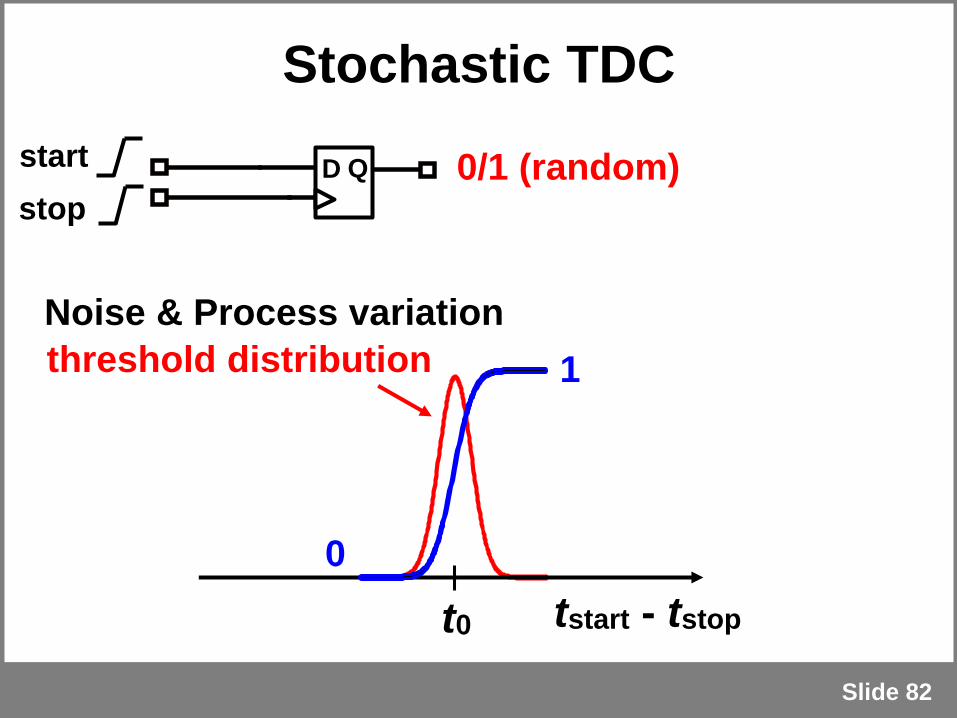
Slide 82
start
stop
D Q 0/1 (random)
threshold distribution
tstart - tstopt0
Noise & Process variation
1
0
Stochastic TDC

Slide 83
*P. M. Levine, et al., IEEE ITC 2004
start
stop
+
D Q
D Q
D Q
D Q
tstart - tstopt0
5
10
15
0
𝟎 ~ 𝒏 − 𝟏
potentially synthesizable
Linearity compensation is
not very difficult.
Output code
Stochastic TDC

Pulse Injection
Slide 84
Free-running
Injection Pulse
Injection locked
*B. Helal, et al., JSSC 2009
• Severe timing design is required on the injection pulse width.

Measured Phase Noise
Slide 85
10k 100k 1M 10M
-120
-80
-40
0
Offset Frequency[Hz]
Ph
as
e N
ois
e [
dB
c/H
z] Frequency: 900MHz
Integrating Jitter: 1.7ps
PDC: 780mW

Simulated Cmedium against Vin
Slide 86
0 0.2 0.4 0.6 0.8
4
8
12
16
Cm
ed
ium
[fF
]
Vin [V]
DM=1
DM=0
Miller effect
PMOS+offsetoffset
NMOS

Fine Varactor
Slide 87
t
Miller effect is gain-dependent.
*W. Deng, et al., ISSCC 2014
A transient variation of VOUT can make a fine
capacitance difference in CIN.

Fine Varactor (cont.)
Slide 88
0 10 20 30
Time[ps]0 10 20 30
Time[ps]
Vin
[V]
VDD
Vin
[V]
VDD
4.8ps0.4ps
Vin
DM=1DM=0DF=0DF=1
Vin
(0.066ps×6)
*W. Deng, et al., ISSCC 2014

Robust for Layout Uncertainty
Slide 89
70m
m
DCO DCO
Hierarchical P&R with
synthesized DCOs
(for comparison)
130 mm
60m
m
110 mm
Fully synthesized
(proposed)
Integrating Jitter: 1.7ps
PDC: 780mW
FOM: -236.5 dB
Integrating Jitter: 2.32ps
PDC: 640mW
FOM: -234.6 dB
DCO DCO