Digital VLSI Design Lecture 1: Introduction · · 2017-02-05Digital VLSI Design Lecture 9: I/O...
19
January 22, 2017 Disclaimer: This course was prepared, in its entirety, by Adam Teman. Many materials were copied from sources freely available on the internet. When possible, these sources have been cited; however, some references may have been cited incorrectly or overlooked. If you feel that a picture, graph, or code example has been copied from you and either needs to be cited or removed, please feel free to email adam [email protected] and I will address this as soon as possible. Digital VLSI Design Lecture 9: I/O and Pad Ring Semester A, 2016-17 Lecturer: Dr. Adam Teman
Transcript of Digital VLSI Design Lecture 1: Introduction · · 2017-02-05Digital VLSI Design Lecture 9: I/O...

January 22, 2017
Disclaimer: This course was prepared, in its entirety, by Adam Teman. Many materials were copied from sources freely available on the internet. When possible, these sources have been cited;
however, some references may have been cited incorrectly or overlooked. If you feel that a picture, graph, or code example has been copied from you and either needs to be cited or removed,
please feel free to email [email protected] and I will address this as soon as possible.
Digital VLSI Design
Lecture 9: I/O and Pad Ring
Semester A, 2016-17
Lecturer: Dr. Adam Teman

A bit about Packaging
2
1
Packaging
2
IOs

How do we get outside the chip?
• It’s actually a pretty long road…• I/O Circuits
• Bonding
• Package
• Board
• Once we get out of the chip• Long wires mean a lot of delay, capacitance, inductance.
• We can use fat wires for low resistance.
• But we have a lot more room to play around.
• The interface between the chip and the outer world is the IC package.

Main Properties of Package• The package provides the physical, temperature and electrical
protection.• Electrical connection from chip to board
• Physical connection from chip to board
• Protection from high voltages (outside)
• Physical protection
• Thermo isolation
• Requirements of a package are:• Electrical: Capacitance, Resistance, Inductance, Impedance Tuning
• Interface: A large number of I/O pins
• Mechanical: Die/Bond protection, Compatibility with PCB
• Thermal: Heat Removal
• Cost: As low cost as possible (without fan, heat sink, etc.)4
Chip
Sig
nal P
ins
Package
Capacitor
Sig
nal P
ads
Chip
VDD
Chip
GND
Board
VDD
Board
GND
Bond Wire Lead Frame
Package

Package to Board Connection
5
DIP(Dual Inline Package)
PGA(Pin Grid Array)
QFP
(Quad Flat Package)
BGA (Ball Grid Array)

IC to Package Connection
Two main approaches:
• Wire bonding• All pads are around
chip edges (~100um pitch).
• Slow, serial bonding process.
• Long, high RLC wires (~5nH, 1pF per wire).
• Flip Chip• Pads on top of IC core.
• High pin count.
• Short, low RLC bonds (0.1nH)
• Fast parallel bonding process.
• But… Expensive!6
Mold Compound
Wire Bond
Die
Die Attach or Sn PlatingSolder or Sn PlantingExposed Die Pad

Input/Output Circuits (I/Os)
7
1
Packaging
2
IOs

So how do we interface to the package?
• We need to create a physical connection to the bonding wire.
• For wire bond packaging:• Use a landing pad.
• Basically a big (100um X 100um) piece of metal.
• Many stacking layers for physical robustness.
• For flip chip packaging:• Use solder bumps.
• Route to bumps withRedistribution Layer(RDL)
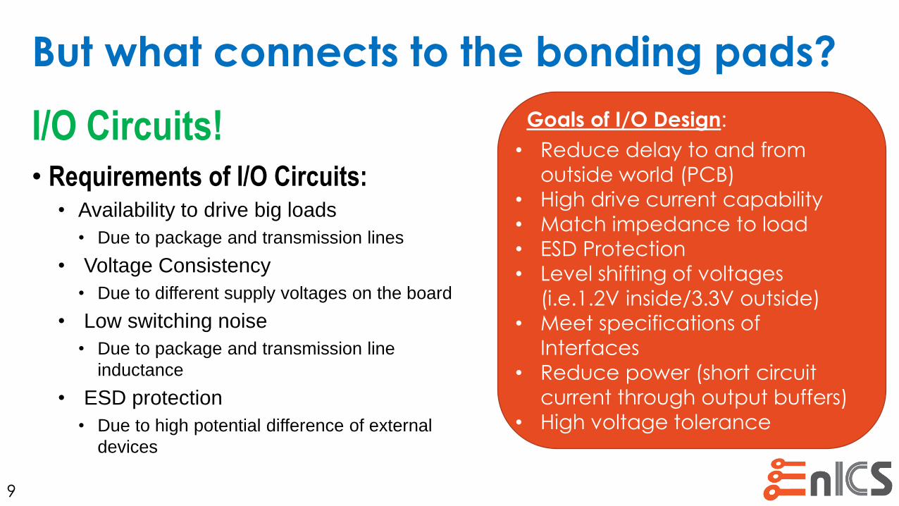
But what connects to the bonding pads?
I/O Circuits! • Requirements of I/O Circuits:
• Availability to drive big loads
• Due to package and transmission lines
• Voltage Consistency
• Due to different supply voltages on the board
• Low switching noise
• Due to package and transmission line
inductance
• ESD protection
• Due to high potential difference of external
devices
9
Goals of I/O Design:
• Reduce delay to and from
outside world (PCB)
• High drive current capability
• Match impedance to load
• ESD Protection
• Level shifting of voltages
(i.e.1.2V inside/3.3V outside)
• Meet specifications of
Interfaces
• Reduce power (short circuit
current through output buffers)
• High voltage tolerance

Types of I/O Cells
There are several types of basic I/O cells:
• Digital I/O Buffers• Provide high drive up-level shifting output
• Provide down-level shifting and ESD protection for inputs
• Analog I/O Cells• Provide ESD protected analog inputs/outputs
• Power supplies• Provide power to the I/O and Core supplies
• Provide the basis for ESD protection
10
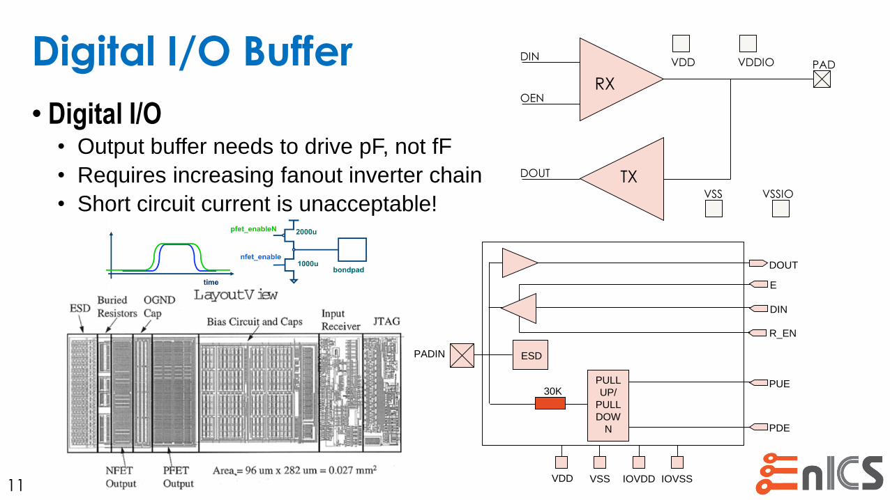
Digital I/O Buffer
• Digital I/O• Output buffer needs to drive pF, not fF
• Requires increasing fanout inverter chain
• Short circuit current is unacceptable!
11
ESDPADIN
DOUT
R_EN
VDD VSS IOVDD IOVSS
30KPULL
UP/
PULL
DOW
N
E
DIN
PUE
PDE
RX
TX
DIN
OEN
DOUT
PADVDD VDDIO
VSS VSSIO
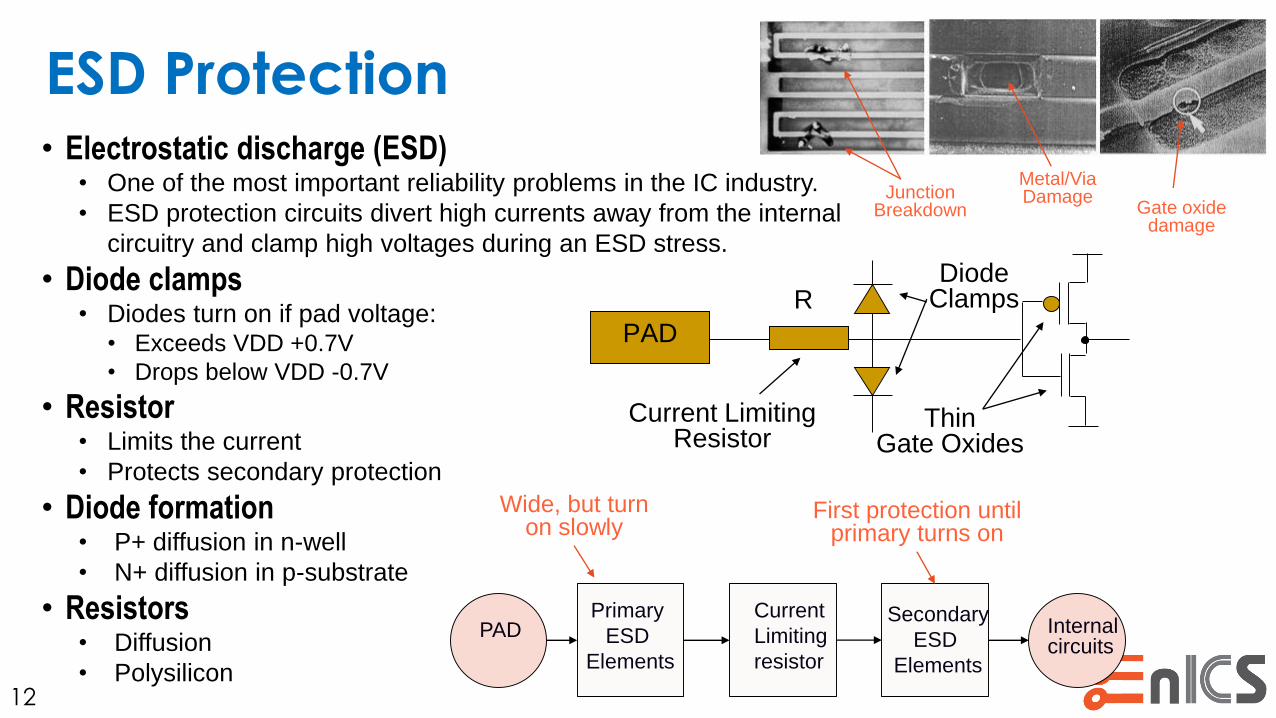
ESD Protection• Electrostatic discharge (ESD)
• One of the most important reliability problems in the IC industry.
• ESD protection circuits divert high currents away from the internal
circuitry and clamp high voltages during an ESD stress.
• Diode clamps• Diodes turn on if pad voltage:
• Exceeds VDD +0.7V
• Drops below VDD -0.7V
• Resistor • Limits the current
• Protects secondary protection
• Diode formation• P+ diffusion in n-well
• N+ diffusion in p-substrate
• Resistors• Diffusion
• Polysilicon12
PAD
RDiode
Clamps
ThinGate Oxides
Current LimitingResistor
Primary
ESD
Elements
Current
Limiting
resistor
Secondary
ESD
Elements
Internalcircuits
PAD
Wide, but turn on slowly
First protection until primary turns on
Junction Breakdown
Metal/Via Damage
Gate oxide damage

Analog I/O Cell
• Analog I/O• Used for passing “analog” signals to/from the chip.
• Basically, “a wire”, but should have some degree of ESD protection.
13
PADNORES
ESD
ESD
IOVDD
IOVSS
PAD
Metal resistor 0.3
Ohm

Power Supply Cells and ESD Protection
• Power supply cells are analog cells (i.e., just a wire).
• But these cells supply the I/O rings for:• Power distribution
• ESD Protection
• Generally, digital (core) and I/O power/ground supplies are separate:• I/Os sink a lot of current Power supply noise
• I/Os usually run at a higher voltage level (i.e., 2.5V vs. 1.2V)
• All (four) types of supplies connect to rings under the I/O circuits.
14
VDDVSSVDDIOVSSIO
IO Cell
Corner
PAD
VSSIO
VDDIO
Digital Input

Simultaneously Switching Outputs
• Simultaneously Switching Outputs (SSO) is a metric describing the period of time during which the switching starts and finishes.• Consider a 64 bit output bus.
• If all transition from high to low, lots of current must driven/sunk leading to extensive voltage drop.
• Problem is independent of frequency
15
SSO-2
Vdrop=Lpackagedi/dt
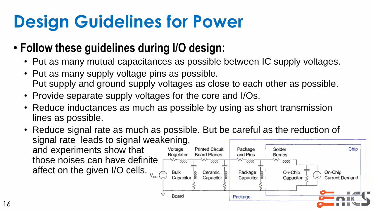
Design Guidelines for Power
• Follow these guidelines during I/O design:• Put as many mutual capacitances as possible between IC supply voltages.
• Put as many supply voltage pins as possible. Put supply and ground supply voltages as close to each other as possible.
• Provide separate supply voltages for the core and I/Os.
• Reduce inductances as much as possible by using as short transmission lines as possible.
• Reduce signal rate as much as possible. But be careful as the reduction of signal rate leads to signal weakening, and experiments show that those noises can have definite affect on the given I/O cells.
16

Pad Configurations
• In-line:• Pads are placed next to each other, with the
corresponding bond pads lined up against each other having a small gap in between.
• Staggered: • Useful technique if design is
“Pad Limited”.
• A larger number of pads can be accommodated in the design, but the overall height of the pad structure increases significantly
17
Corner
Cell
In-Line
Staggered (non-CUP)

Pad Configurations
• Circuit Under Pad (CUP):
• CUP I/O is has the bonding pad over the I/O body itself.
• Bonding pad has to be placed over the I/O body and is
connected to the PAD pin of the I/O.
• CUP I/O can substantially reduce the die size since the
bonding pad does not take any extra space in addition to the
I/O body itself.
• Flip Chip with RDL:
• In the Flip chip methodology, I/O bumps and driver cells
may be placed in the peripheral or in the core area.
• Signals and power are connected to the bumps through
a top aluminum layer called the Redistribution Layer (RDL).
18
Main References
• AMMOS – CDNLive 2007
• IDESA
• CMOS VLSI Design
19