DIGITAL ELECTRONICS: LOGIC AND · PDF fileDIGITAL ELECTRONICS: LOGIC AND CLOCKS ... 74107 JK...
10
1 DIGITAL ELECTRONICS: LOGIC AND CLOCKS LAB 6 INTRO: INTRODUCTION TO DISCRETE DIGITAL LOGIC, MEMORY, AND CLOCKS GOALS In this experiment, we will learn about the most basic elements of digital electronics, from which more complex circuits, including computers, can be constructed. Proficiency with new equipment: o Logic gates, memory circuits, digital clocks DEFINITIONS Duty cycle – percentage of time during one cycle that a system is active (+5V in the case of digital logic) Truth-table – table that shows all possible input combinations and the resulting outputs of digital logic components Flip-flop - a circuit that has two stable states and can be used to store state information. Logic gates – a physical device that implements some Boolean logic operation DIGITAL CIRCUITS - GENERAL In almost all experiments in the physical sciences, the signals that represent physical quantities start out as analog waveforms. To display and analyze the information contained in these signals, they most often are converted to digital data. Often this is done inside a commercial instrument such as an oscilloscope or a lock-in amplifier, which is then connected to a computer through a digital interface. In other cases, data acquisition cards are added to a computer chassis and the analog signals can be input directly to the computer. Scientists usually buy their data acquisition equipment rather than build it, so they often don’t have to know too much about the digital circuitry that makes it work. Almost all data is eventually analyzed with a computer. We emphasize analog electronics in this course because scientists usually have to know much more about it to design and build their experiments. Analog information can be translated into digital form by a device called an Analog-to-Digital Converter (A/D converter or ADC). A set of N bits has 2 N possible different values. You might recall this from Lab #5. If you try to represent an analog voltage by 7 bits, your uncertainty will be about 1%, since there are 2 7 = 128 possible combinations of 7 bits. For higher accuracy you need more bits. The corresponding device that can convert digital data back into an analog waveform is called a Digital-to-Analog Converter (D/A converter or DAC). Logic gates alone can be used to construct arbitrary combinatorial logic (they can generate any truth-table), but to create a machine that steps through a sequence of instructions like a computer does, we also need memory and a clock. The fundamental single-bit memory element of digital electronics is called a flip-flop. We will study two types, called SR (or RS) and JK. The flip-flops we have chosen are also from the TTL family. A digital clock is a repeating digital waveform used to step a digital circuit through a sequence of states. We will introduce the 555 timer chip and use it to generate a clock signal. Digital circuits able to step through a sequence of states with the aid of flip-flops and a clock are called sequential logic. DIGITAL LOGIC STATES The voltage in a digital circuit is allowed to be in only one of two states: HIGH or LOW. HIGH is taken to mean logical (1) or logical TRUE. LOW is taken to mean logical (0) or logical FALSE. In the TTL logic family (see Figure 1), the
Transcript of DIGITAL ELECTRONICS: LOGIC AND · PDF fileDIGITAL ELECTRONICS: LOGIC AND CLOCKS ... 74107 JK...

1
DIGITALELECTRONICS:LOGICANDCLOCKSLAB6INTRO:INTRODUCTIONTODISCRETEDIGITALLOGIC,MEMORY,ANDCLOCKS
GOALSIn this experiment, we will learn about themost basic elements of digital electronics, fromwhichmore
complexcircuits,includingcomputers,canbeconstructed.
Proficiencywithnewequipment:
o Logicgates,memorycircuits,digitalclocks
DEFINITIONS
Dutycycle–percentageoftimeduringonecyclethatasystemisactive(+5Vinthecaseofdigitallogic)Truth-table–tablethatshowsallpossibleinputcombinationsandtheresultingoutputsofdigitallogiccomponentsFlip-flop-acircuitthathastwostablestatesandcanbeusedtostorestateinformation.Logicgates–aphysicaldevicethatimplementssomeBooleanlogicoperation
DIGITALCIRCUITS-GENERALInalmostallexperimentsinthephysicalsciences,thesignalsthatrepresentphysicalquantitiesstartoutas
analogwaveforms.Todisplayandanalyzetheinformationcontainedinthesesignals,theymostoftenareconvertedtodigitaldata.Oftenthisisdoneinsideacommercialinstrumentsuchasanoscilloscopeoralock-inamplifier,whichis then connected to a computer throughadigital interface. In other cases, data acquisition cards are added to acomputer chassis and the analog signals can be input directly to the computer. Scientists usually buy their dataacquisitionequipmentratherthanbuildit,sotheyoftendon’thavetoknowtoomuchaboutthedigitalcircuitrythatmakesitwork.Almostalldataiseventuallyanalyzedwithacomputer.Weemphasizeanalogelectronicsinthiscoursebecausescientistsusuallyhavetoknowmuchmoreaboutittodesignandbuildtheirexperiments.
AnaloginformationcanbetranslatedintodigitalformbyadevicecalledanAnalog-to-DigitalConverter(A/DconverterorADC).AsetofNbitshas2Npossibledifferentvalues. Youmightrecall this fromLab#5. Ifyoutry torepresentananalogvoltageby7bits,youruncertaintywillbeabout1%,sincethereare27=128possiblecombinationsof7bits.Forhigheraccuracyyouneedmorebits.ThecorrespondingdevicethatcanconvertdigitaldatabackintoananalogwaveformiscalledaDigital-to-AnalogConverter(D/AconverterorDAC).
Logicgatesalonecanbeusedtoconstructarbitrarycombinatoriallogic(theycangenerateanytruth-table),buttocreateamachinethatstepsthroughasequenceofinstructionslikeacomputerdoes,wealsoneedmemoryandaclock.Thefundamentalsingle-bitmemoryelementofdigitalelectronicsiscalledaflip-flop.Wewillstudytwotypes,calledSR(orRS)andJK.Theflip-flopswehavechosenarealsofromtheTTLfamily.Adigitalclockisarepeatingdigitalwaveformusedtostepadigitalcircuitthroughasequenceofstates.Wewillintroducethe555timerchipanduseittogenerateaclocksignal.Digitalcircuitsabletostepthroughasequenceofstateswiththeaidofflip-flopsandaclockarecalledsequentiallogic.
DIGITALLOGICSTATES Thevoltageinadigitalcircuitisallowedtobeinonlyoneoftwostates:HIGHorLOW.HIGHistakentomeanlogical(1)orlogicalTRUE.LOWistakentomeanlogical(0)orlogicalFALSE.IntheTTLlogicfamily(seeFigure1),the

2
“ideal”HIGHandLOWvoltagelevelsare5Vand0Vbutanyinputvoltageintherange2to5.0VisinterpretedasHIGH,andanyinputvoltageintherange0to0.8VasLOW.Voltagesoutsidethisrangeareundefined,andtherefore“illegal,”except if theyoccurbrieflyduring transitions. If the input toaTTL circuit is a voltage in thisundefined range, theresponseisunpredictable,withthecircuitsometimesinterpretingitasa“1”andsometimesasa“0.”SeeFig1.
Figure1:TTLInputVoltageLevels
DIGITALLOGICGATES The flow of digital signals is controlled by transistors in various configurations depending on the logic family (see H&H 8.09 for details). For most purposes, we can imagine that the logic gates are composed of ideal switches with just two states: OPEN and CLOSED. The state of a switch is controlled by a digital signal. The switch remains closed so long as a logical (1) signal is applied. A logical (0) control signal keeps it open.
Logic signals interact by means of gates. The three fundamental gates AND, OR, and NOT, are named after the three fundamental operations of logic that they carry out. The AND and OR gates each have two inputs and one output. The output state is determined by the states of the two inputs. The NOT gate has one input and one output. The function of each gate is defined by a truth table, which specifies the output state for each possible combination of input states. The output values of the truth tables can be understood in terms of two switches. If the switches are in series, you get the AND function. Parallel switches perform the OR operation. The most common gates are shown in Fig. 2. A small circle after a gate or at an input on the schematic symbol indicates negation (NOT).

3
Operation Switches Conditionthat
circuitisclosed
Boolean
Notation
Symbol TruthTable
AND
(AANDBareclosed) A•BorAB
OR
(AORBisclosed) A +B
NOT
(sameasinvert)
Different
kindofswitch
1meansopen
0meansclosed
NOT A º A
CompoundGates
NAND
NOR
XOR
Figure2:DigitalLogicgates
A BSeries
AB
A.B A B A.B
0 0 00 1 01 0 01 1 1
AB
A+BA B A+B
0 0 00 1 11 0 11 1 1
A A_ A A
0 11 0
_
AB
A.B
AB
A+B
AB
A + B=AB+AB
Parallel
A
B
4
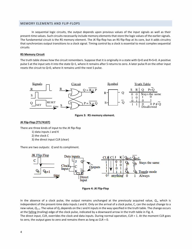
MEMORYELEMENTSANDFLIP-FLOPS In sequential logic circuits, the output depends upon previous values of the input signals aswell as theirpresent-timevalues.Suchcircuitsnecessarilyincludememoryelementsthatstorethelogicvaluesoftheearliersignals.ThefundamentalcircuitistheRSmemoryelement.TheJKflip-flophasanRSflip-flopatitscore,butitaddscircuitrythatsynchronizesoutputtransitionstoaclocksignal.Timingcontrolbyaclockisessentialtomostcomplexsequentialcircuits
RSMemoryCircuit
Thetruthtableshowshowthecircuitremembers.SupposethatitisoriginallyinastatewithQ=0andR=S=0.ApositivepulseSattheinputsetsitintothestateQ=1,whereitremainsafterSreturnstozero.AlaterpulseRontheotherinputresetsthecircuittoQ=0,whereitremainsuntilthenextSpulse.
JKFlip-Flop(TTL74107)
TherearethreekindsofinputtotheJKflip-flop 1)datainputsJandK 2)theclockC 3)thedirectinputCLR(clear)Therearetwooutputs:Qanditscompliment.
Figure4:JKFlip-Flop
In the absence of a clock pulse, the output remains unchanged at the previously acquired value, Qn, which isindependentofthepresent-timedatainputsJandK.Onlyonthearrivalofaclockpulse,C,cantheoutputchangetoanewvalue,Qn+1.ThevalueofQndependsontheJandKinputsinthewayspecifiedinthetruthtable.Thechangeoccursatthefalling(trailing)edgeoftheclockpulse,indicatedbyadownwardarrowinthetruthtableinFig.4.Thedirectinput,CLR,overridestheclockanddatainputs.Duringnormaloperation,CLR=1.AtthemomentCLRgoestozero,theoutputgoestozeroandremainsthereaslongasCLR=0.
Figure3:RSmemoryelement.
RS MEMORYSignals
R
S
Q
R
S
Q = R + P
P = S + Q
Circuit Symbol
R
S
Q
Q
Truth Table
S R Q P=Q0
01
1
0011
Stays the same1 00 10 0Disallowed
P = QSETRESET
time

5
555TimerandDigitalClockSeeFCsection11.14foradescriptionofthegutsofthe555timerchip.Figure9.7showsthecircuitforgeneratingaclockwiththe555andsummarizestheformulasrelatingtheresistorandcapacitorvaluestotheoutputlowtimeT1andtheoutputhightimeT2
(a) Astable circuit (Digital Clock)
1
2
3
4
8
6
5
7
GND
TRIG
OUT
RST
+
DIS
THR
BYP
555
RA
RB
+5V
C0.1uf0V
Output
VC
(b) Component valuesOutput High (charge time): T2 = (RA+RB)C ln2Output Low (discharge): T1 = RBC ln2Period: T = T1 + T2
(c) Limiting ValuesMax RA, RB 3.3 MWMin RA, RB 1 kWMin. C 500pf
V+
.667 V+
.333 V+
time
DC VoltsSupply Voltage (5V)Threshold Level
Trigger Level
Pin 6 - Capacitor Voltage Vc
V+
time
DC Volts Pin 3 Output Voltaget2 t1
C charges through RA and RB in series C discharges through RB only Output is positive while C is charging Output is grounded while C is discharging
(d) Voltage outputs
Figure 9.7 Astable circuit using 555 Timer chip

6
DIGITALLOGICCHIPPINOUTS Eachchiphasadotornotchtoindicatetheendwherepins1and14arelocated.Thepinnumbersincreasesequentiallyasyougocounter-clockwisearoundthechipviewedfromabove.In74xxfamilylogicchips,pin7isalwaysgrounded(0V)andpin14isalwaysconnectedtothe+5Vsupply.
74107JKflip-flop

7
USEFULREADINGS1. FCChapter11(digitalelectronics)2. H&HChapter8.Everythinginthischapterisgoodtoknowaboutbutsections8.01,8.02,8.04,8.07-8.10,
8.12,8.16aremostrelevant.Alsohavealookatsection5.14onthe555timerchip.
LABPREPACTIVITIES
AnswerthefollowingquestionsusingMathematicaordothembyhandinyourlabbook.
Question1
BasicDigitalLogica. Readthelabthoroughlyandenterinyourlabbookthecircuitdiagramsandtruthtablesof
allthecircuitsyouwilltest.TheseincludetheNAND,NOR,andINVERT.b. DesignacircuittoperformtheEXCLUSIVEORfunctionusingonlyNANDand/orNORgates.
SimplifythecircuitsothatyouusethesmallestpossiblenumberofNANDandNORgatesc. CheckthecircuitdoesperformtheEXLUSIVEORusingtruthtablesorBooleanalgebra.
Question2
555Timera. Designa4kHzclockusingthe555-timerchip.Makethelowlevelis1/4oftheoutput
period(25%low,75%high).b. Howlargeacapacitorwouldyouneedtosubstituteinordertomodifyyourclocktorunat
1Hz(e.g.forvisualobservationofLEDs)keepingallothercomponentsfixed?
Question3 JKFlip-flopa. AJKflip-flopwithJ=K=1andCLR=1isdrivenattheclockinputby1kHzpulses.Drawthe
waveformsfortheclockandtheQoutputvs.timeusingthesametimescale.Makesuretoincludeenoughperiodsoftheclocksignaltoseeallthebehavioroftheflip-flop’soutput.
TTLGATES Step1
TruthTables a. Checkyourpowersupplybeforeconnectingtothecircuitboard.TheTektronixPS280/3
hasafixed5Voutputthatyoushouldusetopowerdigitalcircuits.Thelogicchipswillburnoutataround6V.Ifthesupplyvoltagedropswhenyouconnecttothecircuit,donotincreaseV.
b. Inputlogicalvaluescanbesetbyconnectingwiresfromthegateinputstoeither0V(logical0)or5V(logical1).Useonelongrailonyourprototypingboardfor0Vandonefor5V.Note:Disconnectinganinputfromthe5Vrailisnotthesameasconnectingitto0V.Ifitisdisconnected,theinputcanfloatupto5Vonitsown.
c. Thelogicleveloftheoutputcanbeobservedusingalightemittingdiode(LED),whichisconnectedfromtheoutputtoground.TheLEDlightsupwhentheoutputis+5Vandisoffwhentheoutputis0V.Tolimittheamountofcurrentthoughthediode,placearesistorinserieswithit.Whatvalueofresistorshouldyouusetolimitthecurrentto20mA?Recordyourcalculation.
d. RecordthetruthtablesfortheNAND(7400),NOR(7402),andINVERT(7404)gates,usingtheLEDindicatorsforyourmeasurements.
e. ConnectaNANDgatesothat itperformstheINVERTfunction.DothisforaNORgatealso.Thistrickwillbeconvenientinsimplifyingcomplexcircuits.

8
Step2 Modifyingbasicgatesa. ConnectaNANDgatesothat itperformstheINVERTfunction.Dothis foraNORgate
also.Thistrickwillbeconvenientinsimplifyingcomplexcircuits.b. Recordyoucircuitandmeasuredtruthtable.
Step3 ExclusiveORa. VerifythetruthtablesforanEXCLUSIVEORchip(7486).b. NowbuildandtesttheXORcircuitofyourowndesignusingonlyNANDsandNORs.
MEMORYCIRCIUTS
Step4
RSmemorycircuit a. BuildanRSmemorycircuitfromtwoNORgates.Drawaschematicofyourcircuit.b. Demonstratethememorypropertybygoingthroughacompletememorycycle:Set(R=
0,S=1),Store(0,0),Reset(1,0),Store(0,0),Set(0,1).Recordallinputsandoutputsforeachcycle.Doesitagreewithpredictions?
c. Examinetheeffectofthe“illegal”input(R=1,S=1),fordifferentinitialstatesoftheRSsystem.Describetheoutcomesoftheillegaloperation.
TTLCLOCK
Step5
DigitalClock a. Buildthe4kHzdigitalclockusinga555TimeraccordingtoyourdesigninQuestion2of
theprelab.Measurethefrequency,thepulselength(timetheoutputishigh),thedutycycle, and the nominal 5-volt amplitude. Do your measurements agree with yourpredictionsusingthemeasuredvaluesofyourcomponents?
b. Checkthatasuitablelargecapacitorplacedinparallelwiththeexistingoneconvertstheclockto1Hz.
JKFLIP-FLOP
Step6
a. ConstructatruthtablefortheJKflip-flopfromyourobservationsusingtheLEDindicators.Sincetheoutputdependsuponthepreviousstate,Qn,youwillneedtotabulateQn+1forbothpossibleprevious states,Qn=0 andQn=1.We suggest that youaddanadditionalcolumn,Qn+2,togetabetterfeelforthebehavioroftheflip-flop.
b. SetCLR=1andJ=K=1.Nowdrivetheclockinputoftheflip-flopwith4kHzpulsesfromyour clock circuit as shown in Fig. 5.Use theoscilloscope tomeasure the clock input(positivepulsesoutoftheNANDgate),andtheoutput,Q,oftheflip-flop.Recordyourmeasurements.
c. WhathappenswhenJ=K=0?

9
Figure5:JKFlip-floptestset-up
APPENDIX:BOOLEANALGEBRA
Fundamentallaws
Weimaginealogicalvariable,A,thattakesonthevalues0or1.IfA=0thenĀ=1andifA=1thenĀ=0.Hereare
someobviousidentitiesusingtheAND,ORandNOToperations.Lookingattheseidentitiesyoucanseewhythe‘plus’
symbolwaschosenforORand‘times’(•)forAND.
OR AND NOT
A + 0 = A A• 0 = 0 A + A =1A+1=1 A•1= A A• A = 0 A+ A= A A• A= A A = A
A + A =1 A• A = 0
Equality
TwoBooleanexpressionsareequalifandonlyiftheirtruthtablesareidentical.
AssociativeLaws
A + B( )+ C = A+ B + C( )AB( )C = A BC( )
DistributiveLaws
A B + C( )= AB+ ACRelated identities :
A + AB( )= A
A + A B( )= A+ B
A+ B( )• A + C( )= A+ BC( )

10
DeMorgan’sTheorems
A • B • = A + B +
A + B + = A • B •
Example of Proof
Each of the above equalities is a theorem that can be proved. Let’s do an example by directly comparing the truth tables
for the left and right sides. We take on DeMorgan’s first theorem for two variables, AB = A +B
The last columns
of the truth tables are
identical. Thus, the first
theorem is proven for
two variables.
Example of Simplification
Boolean algebra can be used to simplify logical expressions and reduce the number of gates required in a circuit. In Fig.
9.3 we show two ways to implement the expression, Y = A + A BC.
A B AB AB
0 0 0 1
0 1 0 1
1 0 0 1
1 1 1 0
A B A B A + B 0 0 1 1 1
0 1 1 0 1
1 0 0 1 1
1 1 0 0 0
Fig. 9.3. Boolean simplification
A) DIRECT IMPLEMENTATION using NOT, NOR, and NANDA
BC
BC BC
A
ABC ABCA+ABC
Y = A+ABC
B) SIMPLIFIED CIRCUITY = A+ABC
= A+BC (by identity #2)= A+BC (by property of NOT)
= A(BC) (by De Morgan 's Law)
ABC
A
Y = A+ABC