Digital Electronics Chap 1. The Start of the Modern Electronics Era Bardeen, Shockley, and Brattain...
100
Digital Electronics Chap 1
-
Upload
gabriel-day -
Category
Documents
-
view
228 -
download
0
Transcript of Digital Electronics Chap 1. The Start of the Modern Electronics Era Bardeen, Shockley, and Brattain...
Digital Electronics
Chap 1
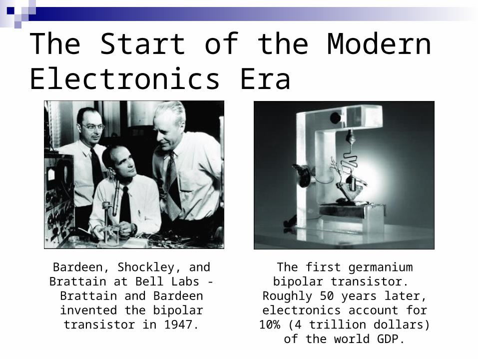
The Start of the Modern Electronics Era
Bardeen, Shockley, and Brattain at Bell Labs - Brattain and Bardeen
invented the bipolar transistor in 1947.
The first germanium bipolar transistor. Roughly 50 years later,
electronics account for 10% (4 trillion dollars) of the world GDP.
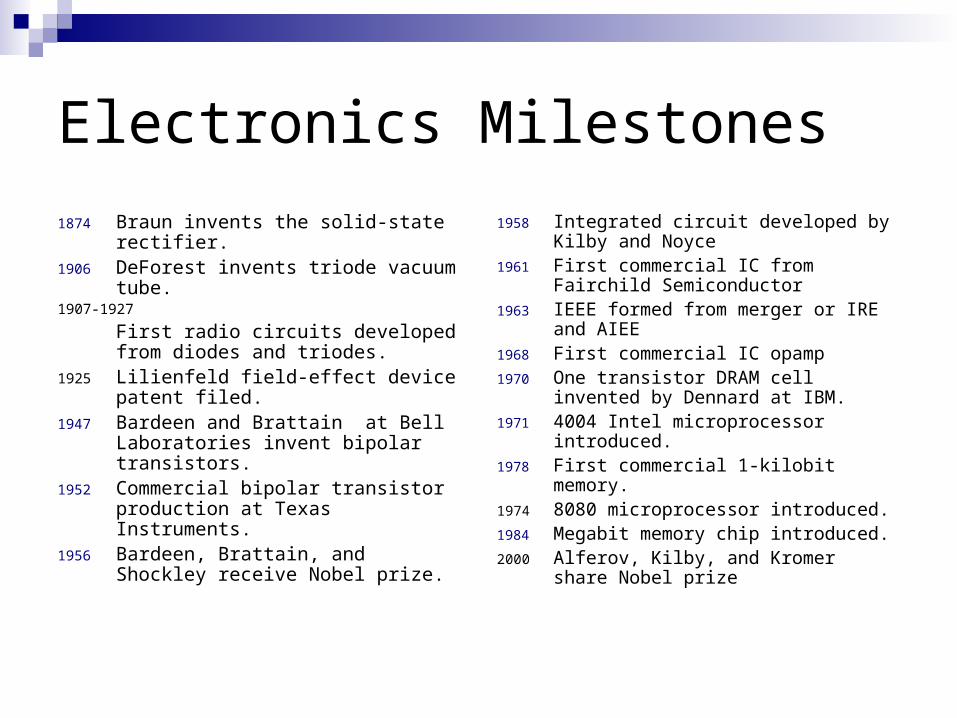
Electronics Milestones
1874 Braun invents the solid-state rectifier.
1906 DeForest invents triode vacuum tube.
1907-1927
First radio circuits developed from diodes and triodes.
1925 Lilienfeld field-effect device patent filed.
1947 Bardeen and Brattain at Bell Laboratories invent bipolar transistors.
1952 Commercial bipolar transistor production at Texas Instruments.
1956 Bardeen, Brattain, and Shockley receive Nobel prize.
1958 Integrated circuit developed by Kilby and Noyce
1961 First commercial IC from Fairchild Semiconductor
1963 IEEE formed from merger or IRE and AIEE
1968 First commercial IC opamp1970 One transistor DRAM cell invented
by Dennard at IBM.1971 4004 Intel microprocessor
introduced.1978 First commercial 1-kilobit memory.1974 8080 microprocessor introduced.1984 Megabit memory chip introduced.2000 Alferov, Kilby, and Kromer share
Nobel prize
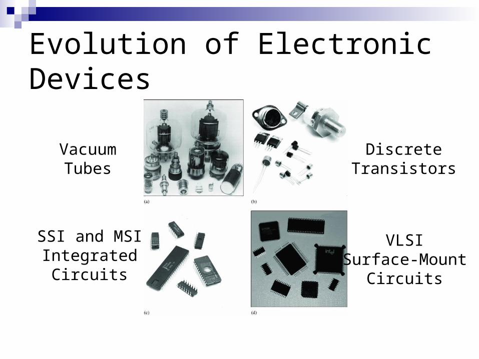
Evolution of Electronic Devices
VacuumTubes
DiscreteTransistors
SSI and MSIIntegratedCircuits
VLSISurface-Mount
Circuits

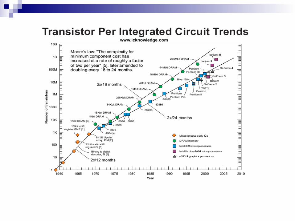
Microelectronics Proliferation
The integrated circuit was invented in 1958. World transistor production has more than doubled every year for
the past twenty years. Every year, more transistors are produced than in all previous years
combined. Approximately 109 transistors were produced in a recent year. Roughly 50 transistors for every ant in the world .
*Source: Gordon Moore’s Plenary address at the 2003 International Solid State Circuits Conference.
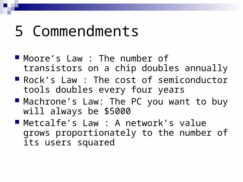
5 Commendments
Moore’s Law : The number of transistors on a chip doubles annually
Rock’s Law : The cost of semiconductor tools doubles every four years
Machrone’s Law: The PC you want to buy will always be $5000
Metcalfe’s Law : A network’s value grows proportionately to the number of its users squared

5 Commandments(cont.)
Wirth’s Law : Software is slowing faster than hardware is accelerating
Further Reading: “5 Commandments”, IEEE Spectrum December 2003, pp. 31-35.

Moore’s law
Moore predicted that the number of transistors that can be integrated on a die would grow exponentially with time.
Amazingly visionary – million transistor/chip barrier was crossed in the 1980’s.
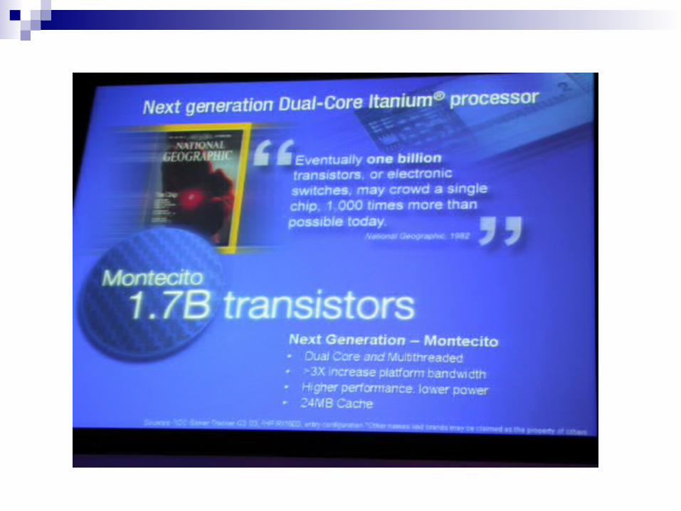
16 M transistors (Ultra Sparc III) 140 M transistor (HP PA-8500) 1.7B transistor (Intel Montecito)

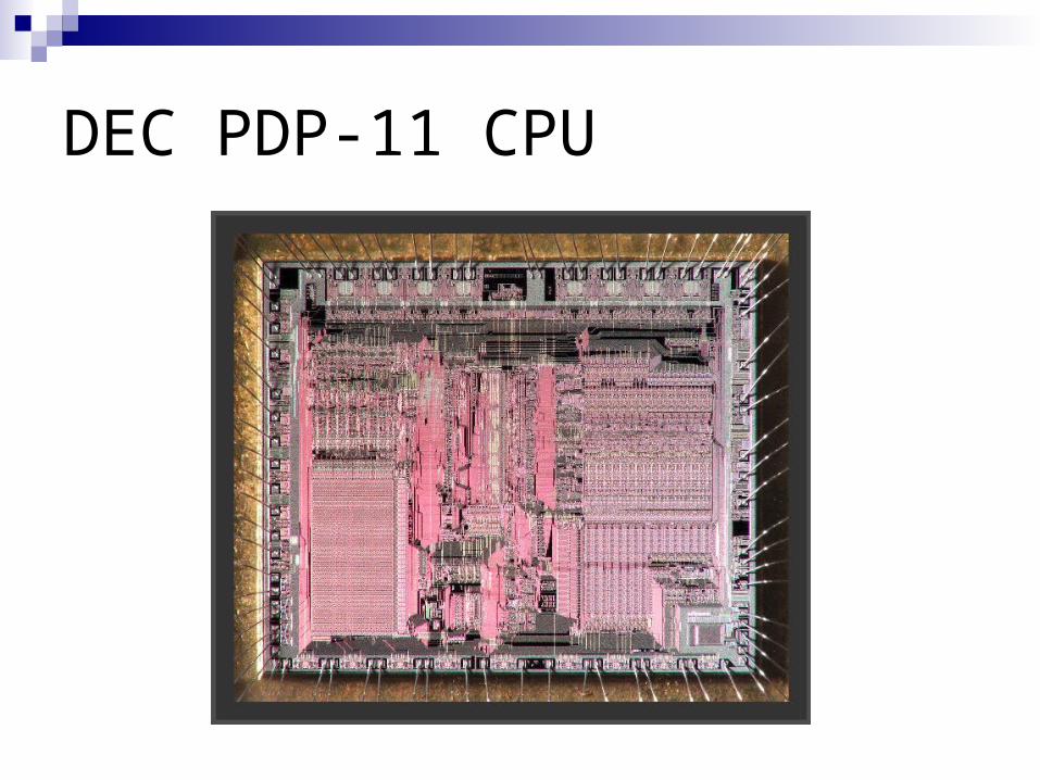
DEC PDP-11 CPU
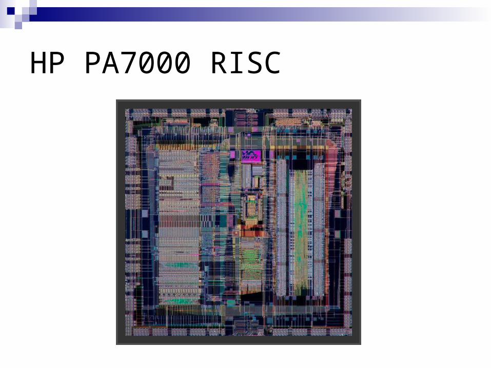
HP PA7000 RISC
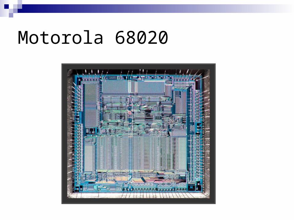
Motorola 68020
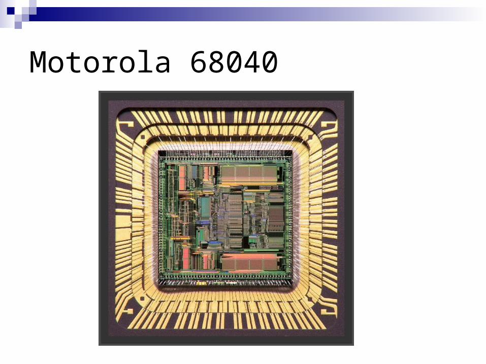
Motorola 68040
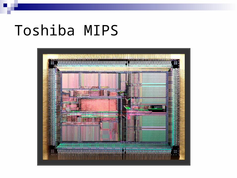
Toshiba MIPS

Intel 8088
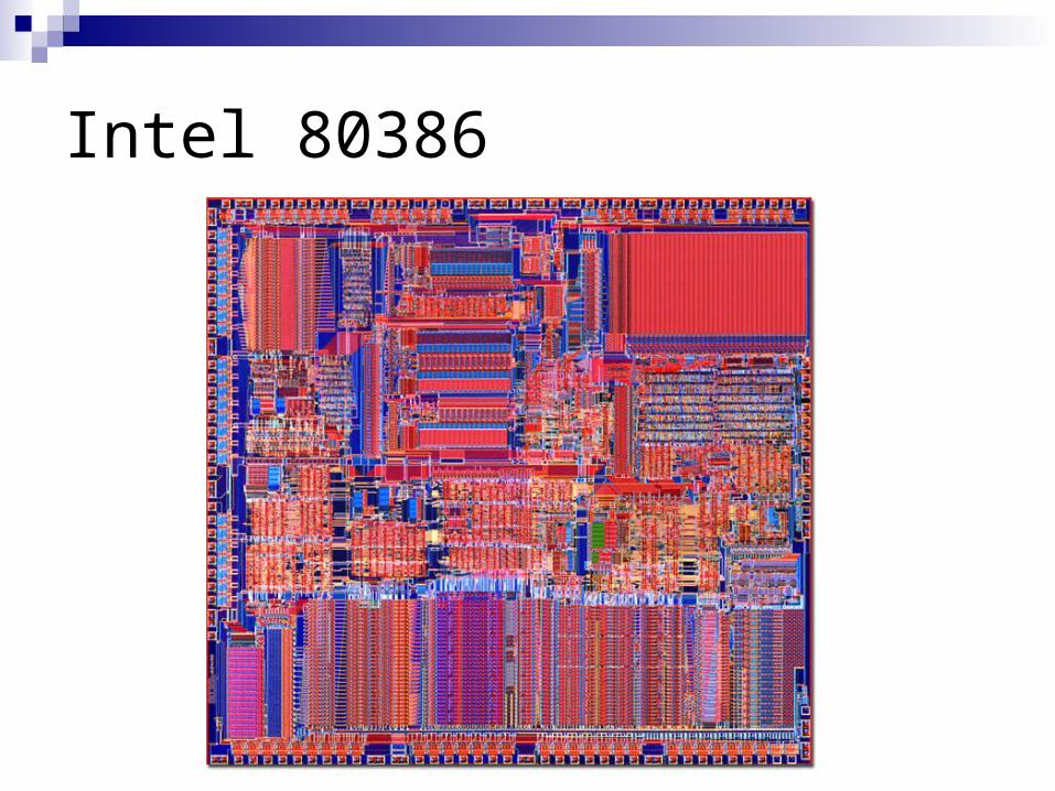
Intel 80386
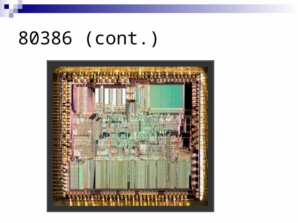
80386 (cont.)
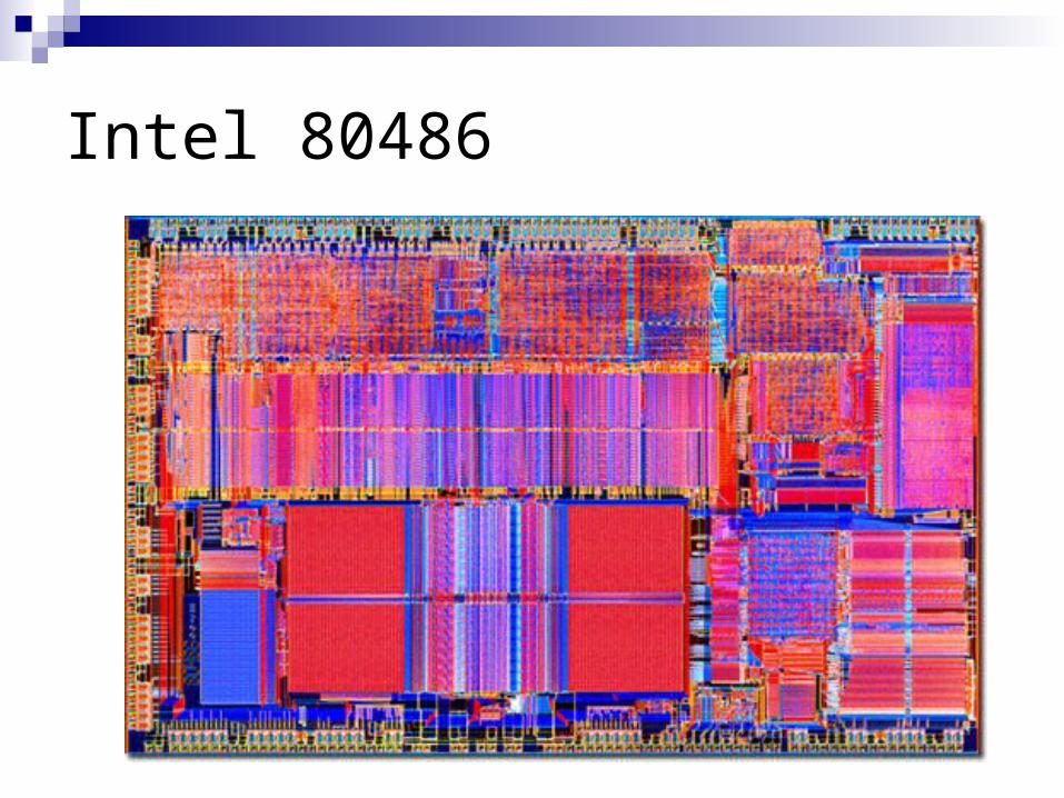
Intel 80486
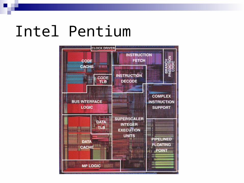
Intel Pentium
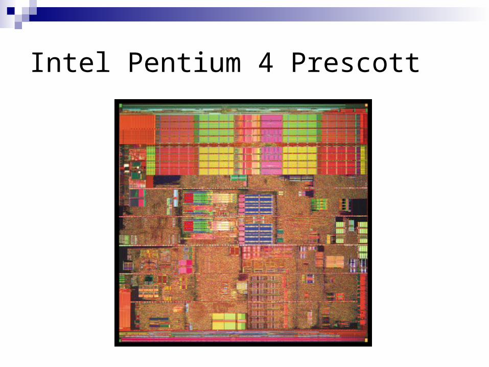
Intel Pentium 4 Prescott

Penryn and Nehalem
Penryn : 45nm Core 2 Architecture : Core 2 Extreme QX9650
Nehalem : Core i7

Intel CPU Evolution

Device Feature Size
Feature size reductions enabled by process innovations.
Smaller features lead to more transistors per unit area and therefore higher density.

Rapid Increase in Density of Microelectronics
Memory chip density versus time.
Microprocessor complexity versus time.

IC Design Step 1: RTL

IC Design 2 : Layout

IC Design 3 : Fabrication

IC Design 4 : Chip
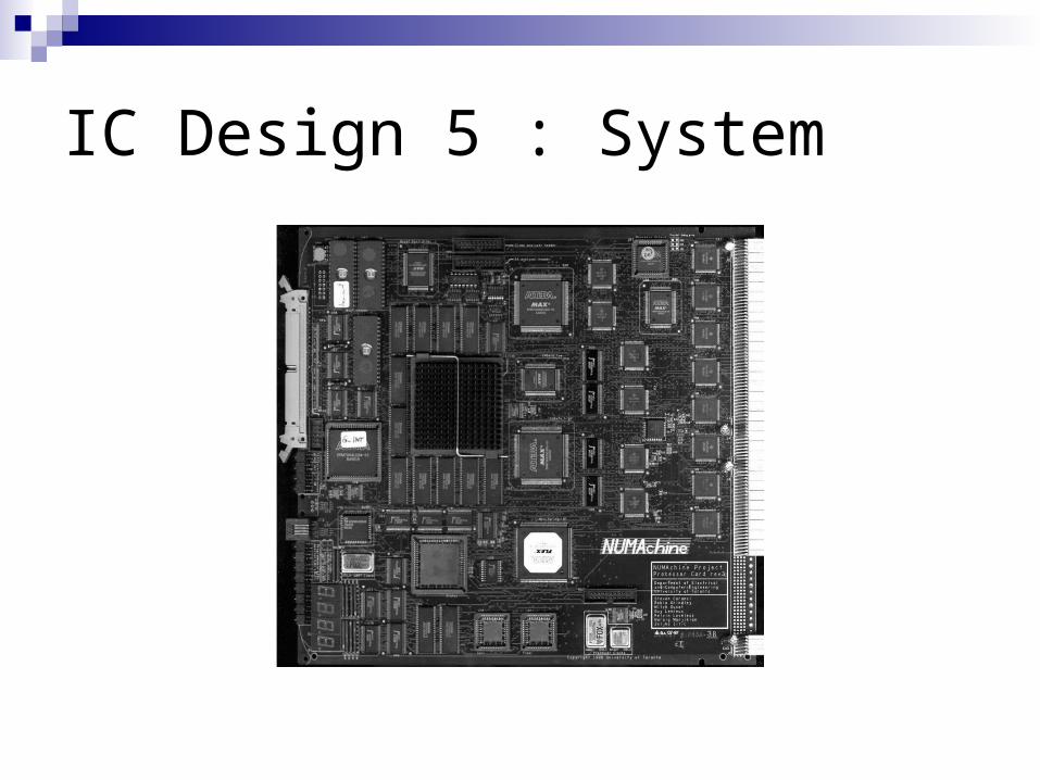
IC Design 5 : System

IC design is mostly coding
Hardware Description Language (Verilog, VHDL) are widely used in today’s IC design.
C programs need to obey rules set by OS. HDL programs need to obey physical rules
in the real world.

Analog versus Digital Electronics Most observables are analog But the most convenient way to represent
and transmit information electronically is digital
Analog/digital and digital/analog conversion is essential


Digital signal representation
By using binary numbers we can represent any quantity. For example a binary two (10) could represent a 2 volt signal. But we generally have to agree on some sort of “code” and the dynamic range of the signal in order to know the form and the minimum number of bits.
Possible digital representation for a pure sine wave of known frequency. We must choose maximum value and “resolution” or “error,” then we can encode the numbers. Suppose we want 1V accuracy of amplitude with maximum amplitude of 50V, we could use a simple pure binary code with 6 bits of information.

Digital representations of logical functions Digital signals also offer an effective way to execute
logic. The formalism for performing logic with binary variables is called switching algebra or boolean algebra.
Digital electronics combines two important properties: The ability to represent real functions by coding the
information in digital form. The ability to control a system by a process of
manipulation and evaluation of digital variables using switching algebra.
Digital Representations of logic functions (cont.) Digital signals can be transmitted, received,
amplified, and retransmitted with no degradation. Binary numbers are a natural method of expressing
logic variables. Complex logic functions are easily expressed as
binary function. With digital representation, we can achieve arbitrary
levels of “ dynamic range,” that is, the ratio of the largest possible signal to the smallest than can be distinguished above the background noise.
Digital information is easily and inexpensively stored
Signal Types
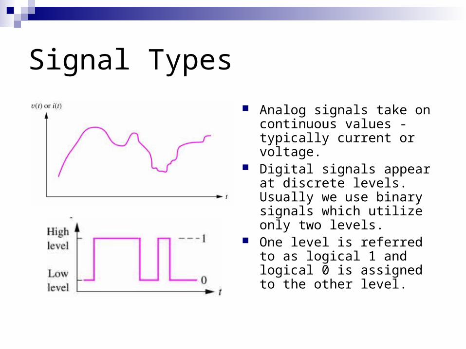
Analog signals take on continuous values - typically current or voltage.
Digital signals appear at discrete levels. Usually we use binary signals which utilize only two levels.
One level is referred to as logical 1 and logical 0 is assigned to the other level.

Analog and Digital Signals
Analog signals are continuous in time and voltage or current. (Charge can also be used as a signal conveyor.)
After digitization, the continuous analog signal becomes a set of discrete values, typically separated by fixed time intervals.
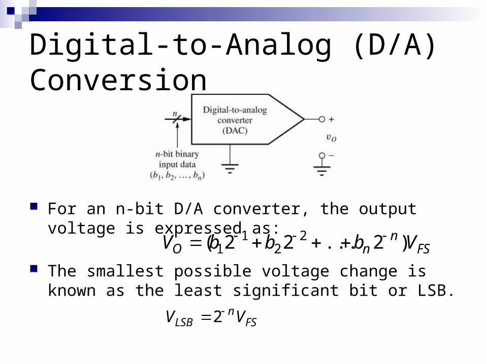
Digital-to-Analog (D/A) Conversion
For an n-bit D/A converter, the output voltage is expressed as:
The smallest possible voltage change is known as the least significant bit or LSB.
VLSB 2 nVFS
VO (b12 1 b2 2 2 ...bn 2 n )VFS
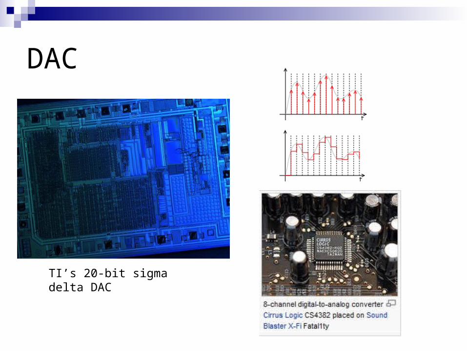
DAC
TI’s 20-bit sigma delta DAC
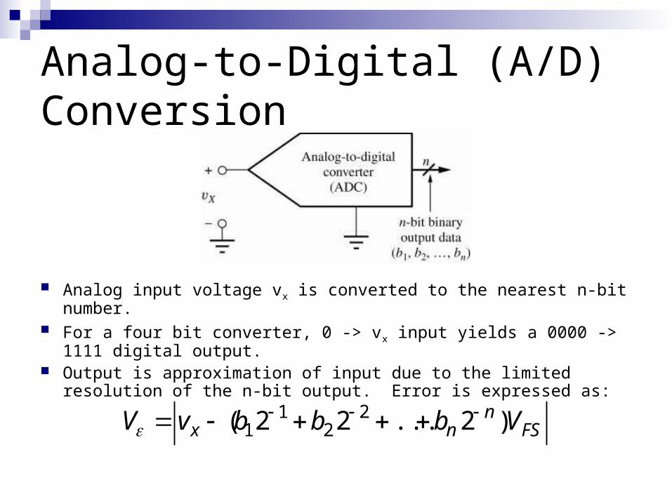
Analog-to-Digital (A/D) Conversion
Analog input voltage vx is converted to the nearest n-bit number. For a four bit converter, 0 -> vx input yields a 0000 -> 1111 digital
output. Output is approximation of input due to the limited resolution of the
n-bit output. Error is expressed as:
V vx (b12 1 b2 2 2 ...bn 2 n )VFS
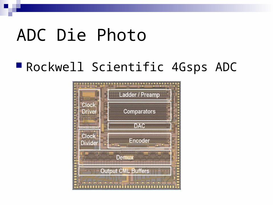
ADC Die Photo
Rockwell Scientific 4Gsps ADC

A/D Converter Transfer Characteristic
V vx (b12 1 b2 2 2 ...bn 2 n )VFS
Introduction to Circuit Theory
Circuit theory is based on the concept of modeling. To analyze any complex physical system, we must be able to describe the system in terms of an idealized model that is an interconnection of idealized elements.
By analyzing the circuit model, we can predict the behavior of the physical circuit and design better circuits.

Lumped Circuits
Lumped circuits are obtained by connecting lumped elements.
Typical lumped elements are resistors, capacitors, inductors, and transformers.
The size of lumped circuit is small compared to the wavelength of their normal frequency of operation.
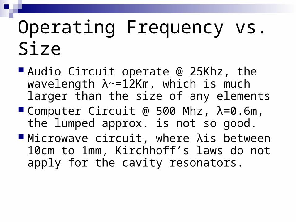
Operating Frequency vs. Size
Audio Circuit operate @ 25Khz, the wavelength λ~=12Km, which is much larger than the size of any elements
Computer Circuit @ 500 Mhz, λ=0.6m, the lumped approx. is not so good.
Microwave circuit, where λis between 10cm to 1mm, Kirchhoff’s laws do not apply for the cavity resonators.
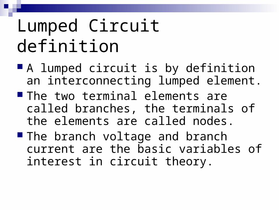
Lumped Circuit definition
A lumped circuit is by definition an interconnecting lumped element.
The two terminal elements are called branches, the terminals of the elements are called nodes.
The branch voltage and branch current are the basic variables of interest in circuit theory.

Lumped circuit figure

Reference Directions
A two terminal lumped elements (branch) with nodes A and B.
The reference directions for the branch voltage v and branch current i are shown in the graph.
The reference direction is chosen arbitrarily.
+
-
v
i
A
B
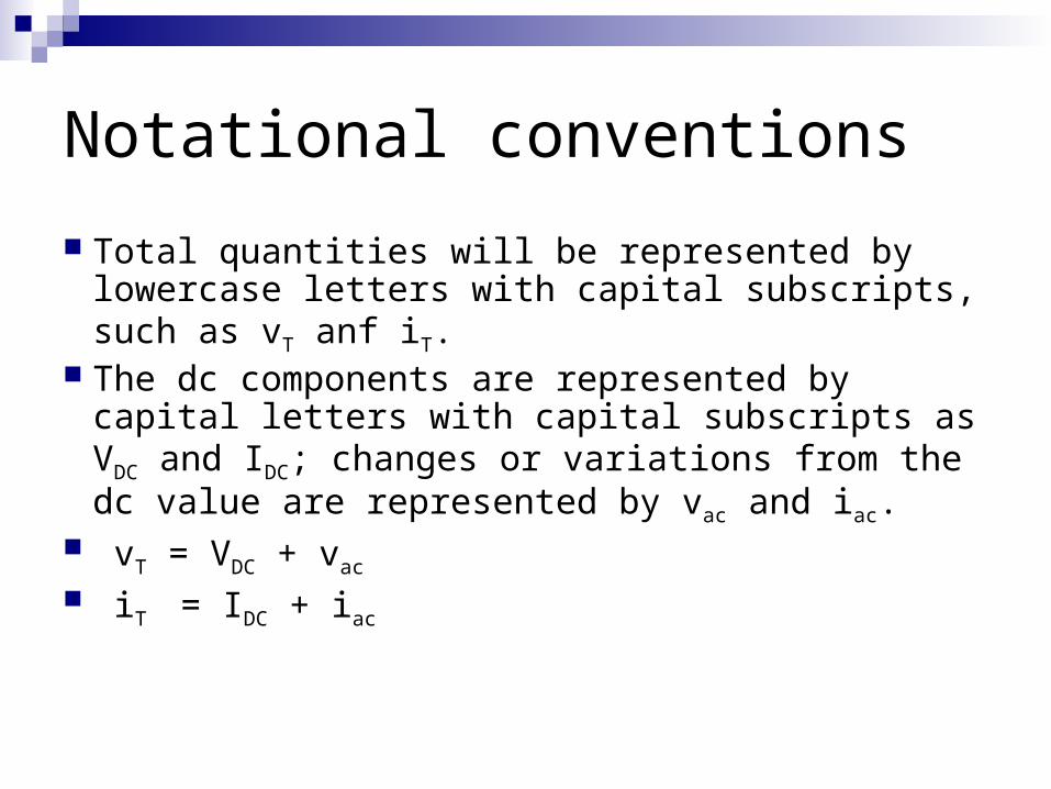
Notational conventions
Total quantities will be represented by lowercase letters with capital subscripts, such as vT anf iT.
The dc components are represented by capital letters with capital subscripts as VDC and IDC; changes or variations from the dc value are represented by vac and iac.
vT = VDC + vac iT = IDC + iac

i1i 1
(b) CCCS
i1 1i
(d) CCVS
1A vv1
+
-
(c) VCVS
g vm 1v1
+
-
(a) VCCS
Figure 1.10 - Controlled Sources
(a) Voltage-controlled current source - (VCCS)
(b)Current-controlled current source - (CCCS)
(c) Voltage-controlled voltage source - (VCVS)
(d) Current-controlled voltage source - (CCVS).
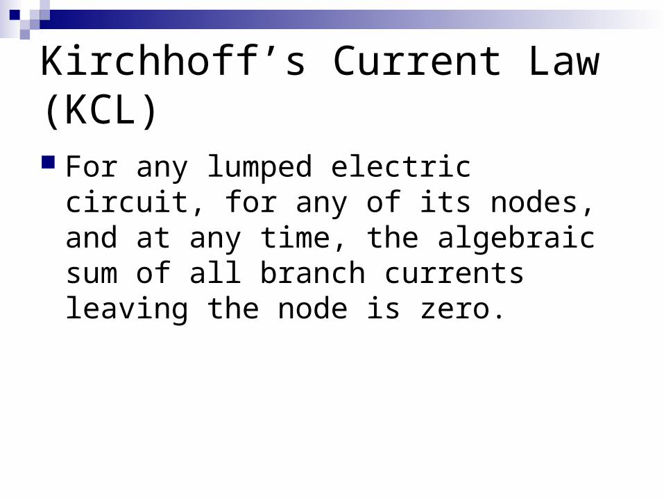
Kirchhoff’s Current Law (KCL)
For any lumped electric circuit, for any of its nodes, and at any time, the algebraic sum of all branch currents leaving the node is zero.

KCL Example
When applying KCL to circuit, first assign reference direction for each branch.
For node 2, i4-i3-i6=0
For node 1, -i1+i2+i3=0
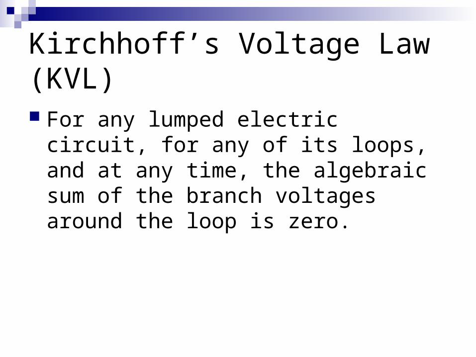
Kirchhoff’s Voltage Law (KVL)
For any lumped electric circuit, for any of its loops, and at any time, the algebraic sum of the branch voltages around the loop is zero.
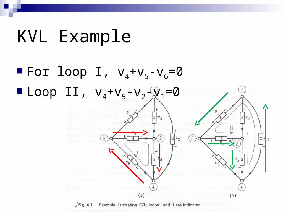
KVL Example
For loop I, v4+v5-v6=0
Loop II, v4+v5-v2-v1=0
Properties of KCL and KVL
KCL imposes a linear constraint on the branch currents.
KCL applies to any lumped electric circuit; it is independent of the nature of the elements.
KCL expresses the conservation of charge at any time.

Properties of KVL and KCL (cont.)
An example where KCL doesn’t apply is the whip antenna. The antenna is about ¼ wavelength so it is not a lumped circuit.
KVL imposes a linear constraint between branch voltages of a loop.
KVL is independent of the natural of the elements.
Circuit Elements
Resistors Independent sources Capacitors Inductors

被動元件
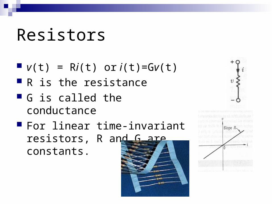
Resistors
v(t) = Ri(t) or i(t)=Gv(t) R is the resistance G is called the conductance For linear time-invariant resistors,
R and G are constants.
Independent Sources
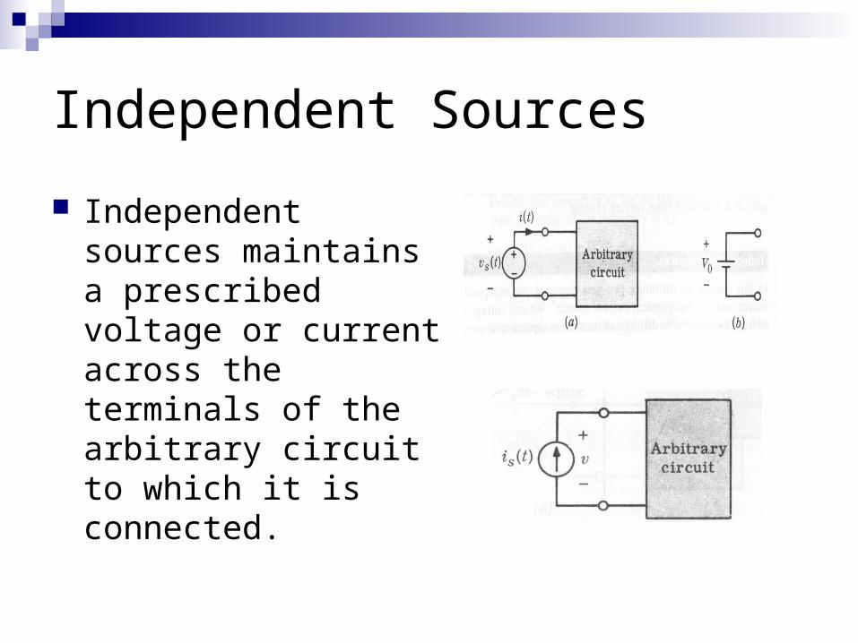
Independent sources maintains a prescribed voltage or current across the terminals of the arbitrary circuit to which it is connected.
Capacitors
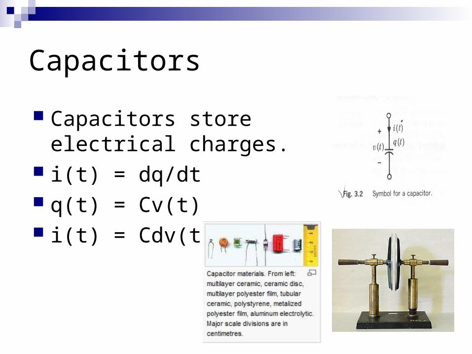
Capacitors store electrical charges.
i(t) = dq/dt q(t) = Cv(t) i(t) = Cdv(t)/dt
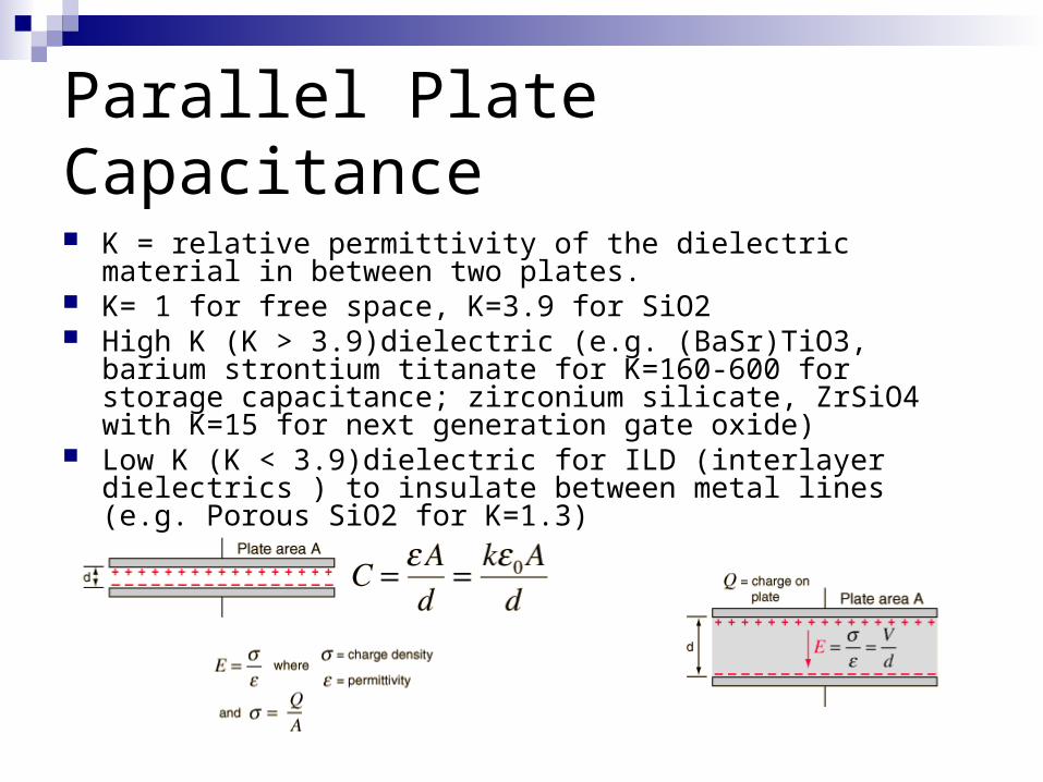
Parallel Plate Capacitance
K = relative permittivity of the dielectric material in between two plates.
K= 1 for free space, K=3.9 for SiO2 High K (K > 3.9)dielectric (e.g. (BaSr)TiO3, barium strontium titanate
for K=160-600 for storage capacitance; zirconium silicate, ZrSiO4 with K=15 for next generation gate oxide)
Low K (K < 3.9)dielectric for ILD (interlayer dielectrics ) to insulate between metal lines (e.g. Porous SiO2 for K=1.3)
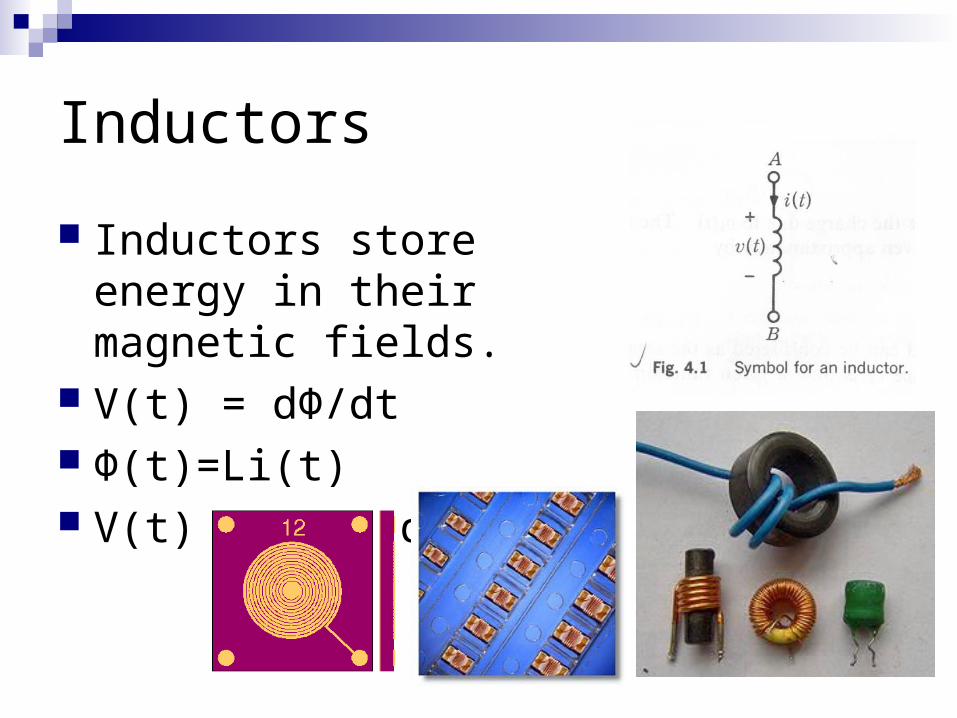
Inductors
Inductors store energy in their magnetic fields.
V(t) = dΦ/dt Φ(t)=Li(t) V(t) = L di/dt

RLC Effects in Real Circuit
Power (Thermal) Time Delay
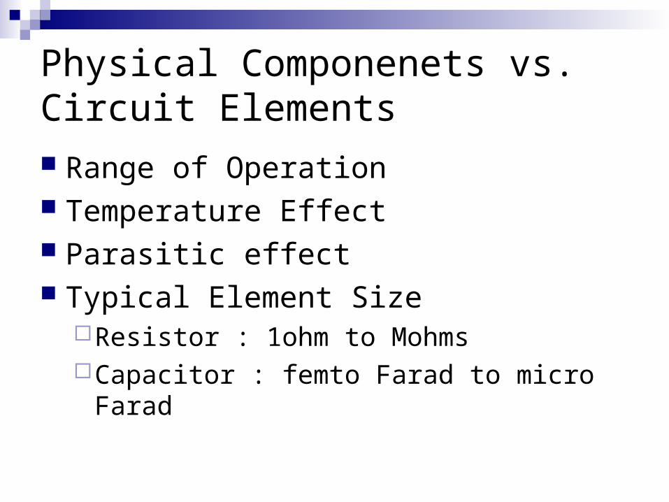
Physical Componenets vs. Circuit Elements Range of Operation Temperature Effect Parasitic effect Typical Element Size
Resistor : 1ohm to MohmsCapacitor : femto Farad to micro Farad
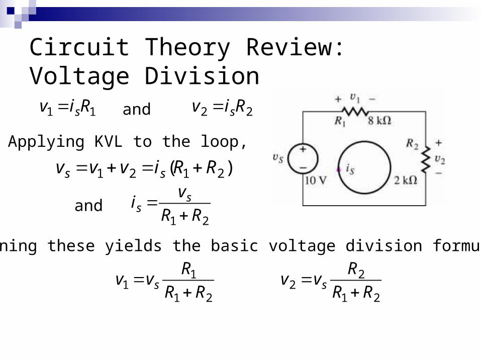
Circuit Theory Review: Voltage Division
v1 isR1
v2 isR2
and
vs v1 v2 is (R1 R2)
is vs
R1 R2
v1 vsR1
R1 R2
v2 vsR2
R1 R2
Applying KVL to the loop,
Combining these yields the basic voltage division formula:
and
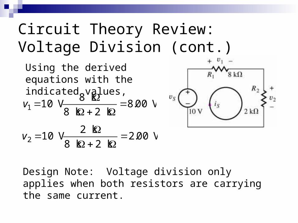
v1 10 V8 k
8 k 2 k8.00 V
Using the derived equations with the indicated values,
v2 10 V2 k
8 k 2 k2.00 V
Design Note: Voltage division only applies when both resistors are carrying the same current.
Circuit Theory Review: Voltage Division (cont.)
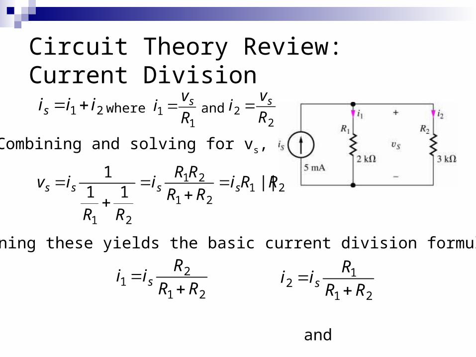
Circuit Theory Review: Current Division
is i1 i2
and
i1 isR2
R1 R2
Combining and solving for vs,
Combining these yields the basic current division formula:
where
i2 vsR2
i1 vsR1
and
vs is1
1
R1
1
R2
isR1R2
R1 R2
isR1 || R2
i2 isR1
R1 R2

Circuit Theory Review: Current Division (cont.)
i1 5 ma3 k
2 k 3 k3.00 mA
Using the derived equations with the indicated values,
Design Note: Current division only applies when the same voltage appears across both resistors.
i2 5 ma2 k
2 k 3 k2.00 mA

Equivalent Circuit
Thevenin and Norton Equivalent circuit represents real-world battery models.
Complex circuits can be simplified to these representation to help us understand the circuits.

Circuit Theory Review: Thevenin and Norton Equivalent Circuits
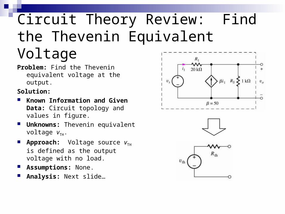
Circuit Theory Review: Find the Thevenin Equivalent Voltage
Problem: Find the Thevenin equivalent voltage at the output.
Solution: Known Information and Given
Data: Circuit topology and values in figure.
Unknowns: Thevenin equivalent voltage vTH.
Approach: Voltage source vTH is defined as the output voltage with no load.
Assumptions: None. Analysis: Next slide…
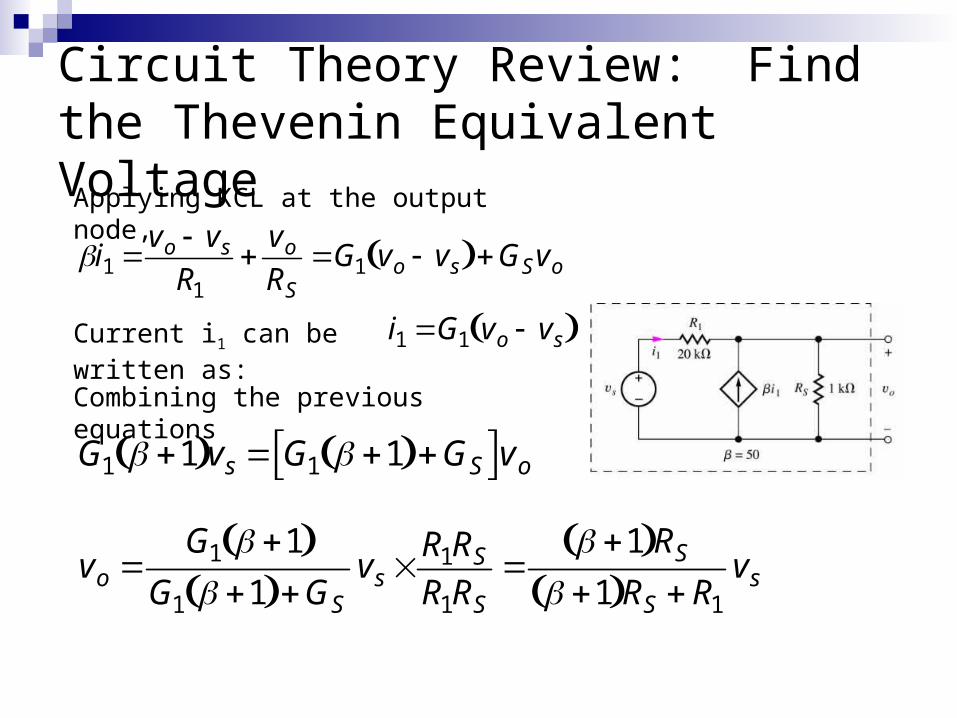
Circuit Theory Review: Find the Thevenin Equivalent Voltage
i1 vo vsR1
voRS
G1 vo vs GSvo
i1 G1 vo vs
G1 1 vs G1 1 GS vo
vo G1 1
G1 1 GSvs
R1RSR1RS
1 RS
1 RS R1
vs
Applying KCL at the output node,
Current i1 can be written as:
Combining the previous equations

Circuit Theory Review: Find the Thevenin Equivalent Voltage (cont.)
vo 1 RS
1 RS R1
vs 501 1 k
501 1 k 1 kvs 0.718vs
Using the given component values:
and
vTH 0.718vs

Circuit Theory Review: Find the Thevenin Equivalent ResistanceProblem: Find the Thevenin
equivalent resistance.
Solution: Known Information and Given
Data: Circuit topology and values in figure.
Unknowns: Thevenin equivalent resistance RTH.
Approach: RTH is defined as the equivalent resistance at the output terminals with all independent sources in the network set to zero.
Assumptions: None. Analysis: Next slide…
Test voltage vx has been added to the previous circuit. Applying vx and solving for ix allows us to find the Thevenin resistance as vx/ix.
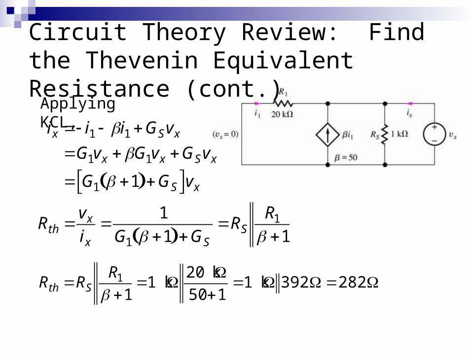
Circuit Theory Review: Find the Thevenin Equivalent Resistance (cont.)
ix i1 i1 GSvxG1vx G1vx GSvx G1 1 GS vx
Rth vxix
1
G1 1 GSRS
R1
1
Applying KCL,
Rth RSR1
11 k
20 k501
1 k 392 282
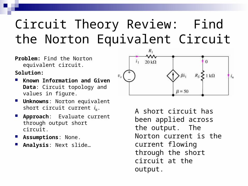
Circuit Theory Review: Find the Norton Equivalent Circuit
Problem: Find the Norton equivalent circuit.
Solution: Known Information and Given
Data: Circuit topology and values in figure.
Unknowns: Norton equivalent short circuit current iN.
Approach: Evaluate current through output short circuit.
Assumptions: None. Analysis: Next slide…
A short circuit has been applied across the output. The Norton current is the current flowing through the short circuit at the output.
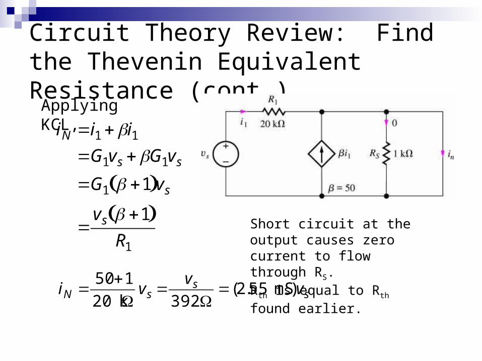
Circuit Theory Review: Find the Thevenin Equivalent Resistance (cont.)
iN i1 i1G1vs G1vsG1 1 vs
vs 1 R1
Applying KCL,
iN 501
20 kvs
vs392
(2.55 mS)vs
Short circuit at the output causes zero current to flow through RS.Rth is equal to Rth found earlier.
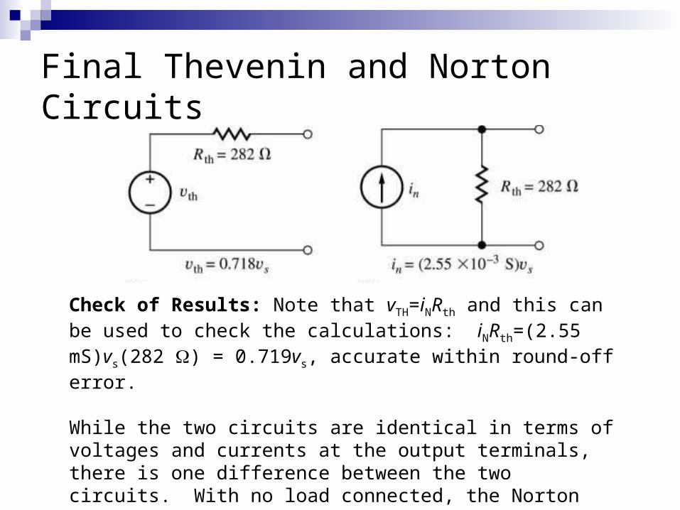
Final Thevenin and Norton Circuits
Check of Results: Note that vTH=iNRth and this can be used to check the calculations: iNRth=(2.55 mS)vs(282 ) = 0.719vs, accurate within round-off error.
While the two circuits are identical in terms of voltages and currents at the output terminals, there is one difference between the two circuits. With no load connected, the Norton circuit still dissipates power!

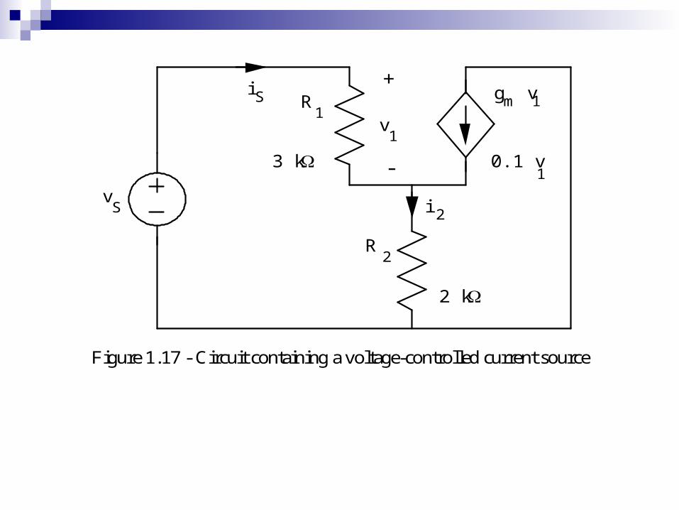
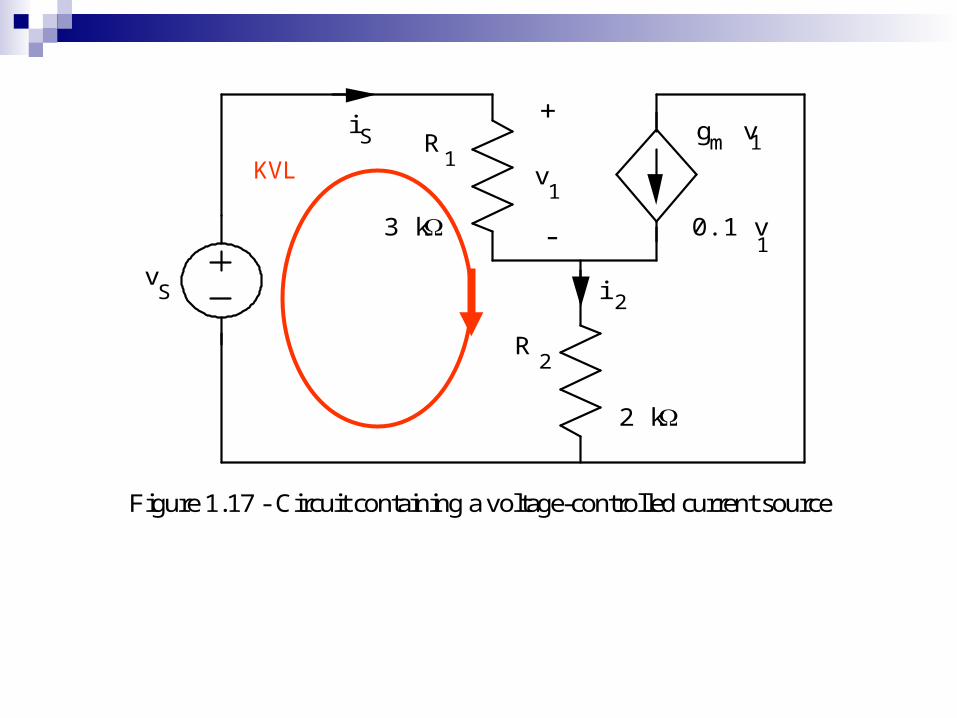
Example : Circuit with a controlled source Applying KVL around the loop containing vs
yields vs = isR1 + i2R2 = isR1 + (is + gmv1)R2 (1.33) v1 = isR1 (1.34) vs = is(R1 + R2 + gmR1R2) (1.35) Req = vs / is = R1 + R2 (1+ gmR1) (1.36) Req = 3KΩ+2KΩ[1+0.1S*3KΩ] = 605 kΩ. This
value is far larger than either R1 or R2.
R1
R2
iS
vS 2i
g vm 1+
-
v1
2 k
3 k 0.1 v1
Figure 1.17 - Circuit containing a voltage-controlled current source
R1
R2
iS
vS 2i
g vm 1+
-
v1
2 k
3 k 0.1 v1
Figure 1.17 - Circuit containing a voltage-controlled current source
KVL

Circuitry Snacks
from : www.evilmadscientist.com

Joule Thief
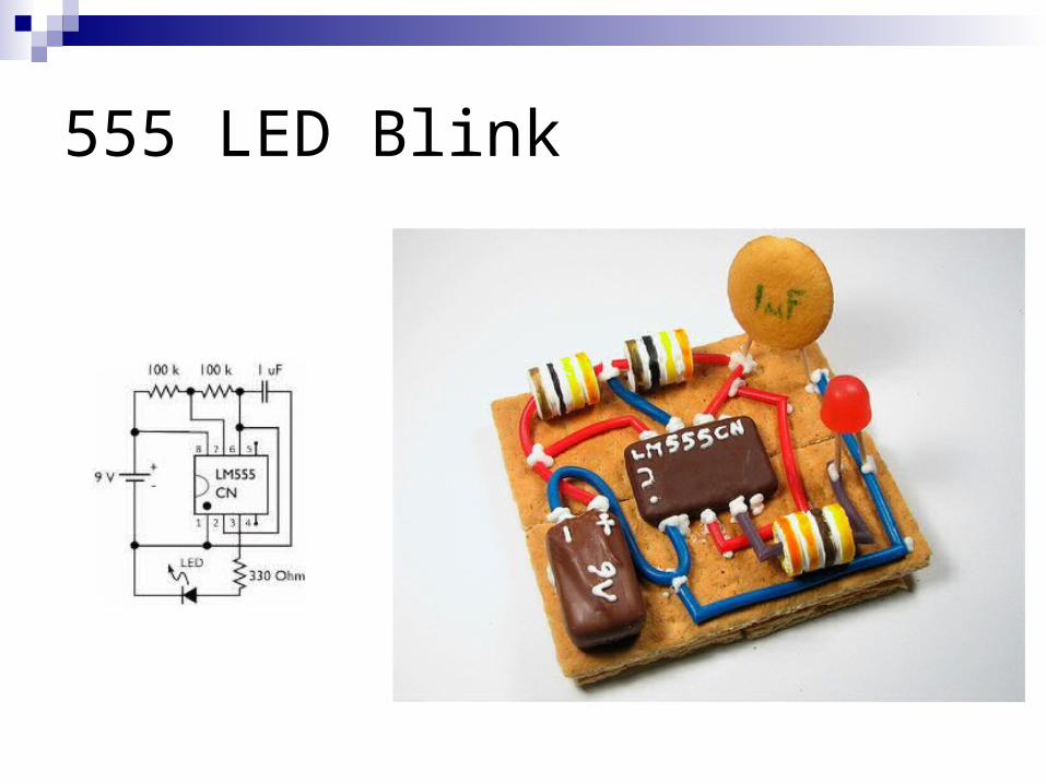
555 LED Blink
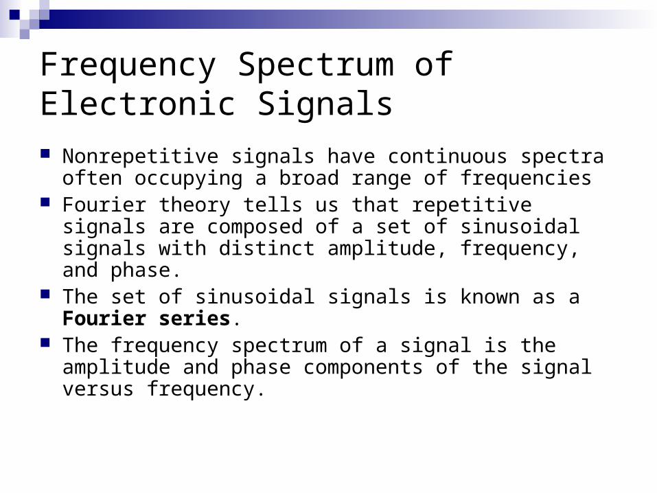
Frequency Spectrum of Electronic Signals Nonrepetitive signals have continuous spectra often
occupying a broad range of frequencies Fourier theory tells us that repetitive signals are
composed of a set of sinusoidal signals with distinct amplitude, frequency, and phase.
The set of sinusoidal signals is known as a Fourier series.
The frequency spectrum of a signal is the amplitude and phase components of the signal versus frequency.
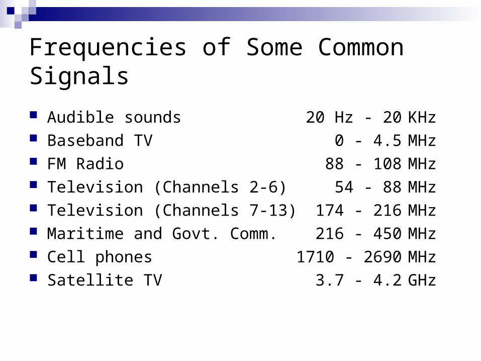
Frequencies of Some Common Signals
Audible sounds 20 Hz - 20 KHz Baseband TV 0 - 4.5 MHz FM Radio 88 - 108 MHz Television (Channels 2-6) 54 - 88 MHz Television (Channels 7-13) 174 - 216 MHz Maritime and Govt. Comm. 216 - 450 MHz Cell phones 1710 - 2690 MHz Satellite TV 3.7 - 4.2 GHz
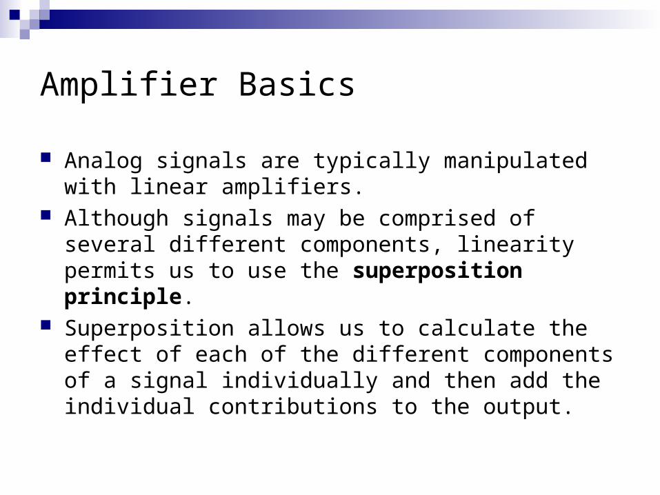
Amplifier Basics
Analog signals are typically manipulated with linear amplifiers.
Although signals may be comprised of several different components, linearity permits us to use the superposition principle.
Superposition allows us to calculate the effect of each of the different components of a signal individually and then add the individual contributions to the output.

RF Amplifier and Filter
MixerIF
Amplifier and Filter
Local Oscillator
FM Detector
Audio Amplifier
Speaker
10.7 MHz 50 Hz - 15 kHz(88 - 108 MHz)
(77.3 - 97.3 MHz)
Antenna
Figure 1.21 - Block diagram for an FM radio Receiver

Amplifier Input/Output Response
vs = sin2000t V
Av = -5
Note: negative gain is equivalent to 180 degress of phase shift.

Amplifier Frequency Response
Low-Pass High-Pass BandPass Band-Reject All-Pass
Amplifiers can be designed to selectively amplify specific ranges of frequencies. Such an amplifier is known as a filter. Several filter types are shown below:

Circuit Element Variations
All electronic components have manufacturing tolerances. Resistors can be purchased with 10%, 5%, and
1% tolerance. (IC resistors are often 10%.) Capacitors can have asymmetrical tolerances such as +20%/-50%. Power supply voltages typically vary from 1% to 10%.
Device parameters will also vary with temperature and age. Circuits must be designed to accommodate these variations. We will use worst-case and Monte Carlo (statistical) analysis to
examine the effects of component parameter variations.
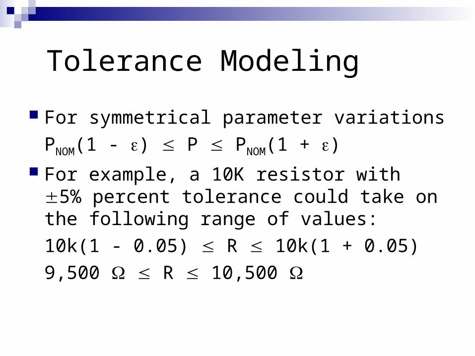
Tolerance Modeling
For symmetrical parameter variations
PNOM(1 - ) P PNOM(1 + ) For example, a 10K resistor with 5%
percent tolerance could take on the following range of values:
10k(1 - 0.05) R 10k(1 + 0.05)
9,500 R 10,500

Circuit Analysis with Tolerances
Worst-case analysis Parameters are manipulated to produce the worst-case min and max
values of desired quantities. This can lead to over design since the worst-case combination of
parameters is rare. It may be less expensive to discard a rare failure than to design for 100%
yield. Monte-Carlo analysis
Parameters are randomly varied to generate a set of statistics for desired outputs.
The design can be optimized so that failures due to parameter variation are less frequent than failures due to other mechanisms.
In this way, the design difficulty is better managed than a worst-case approach.
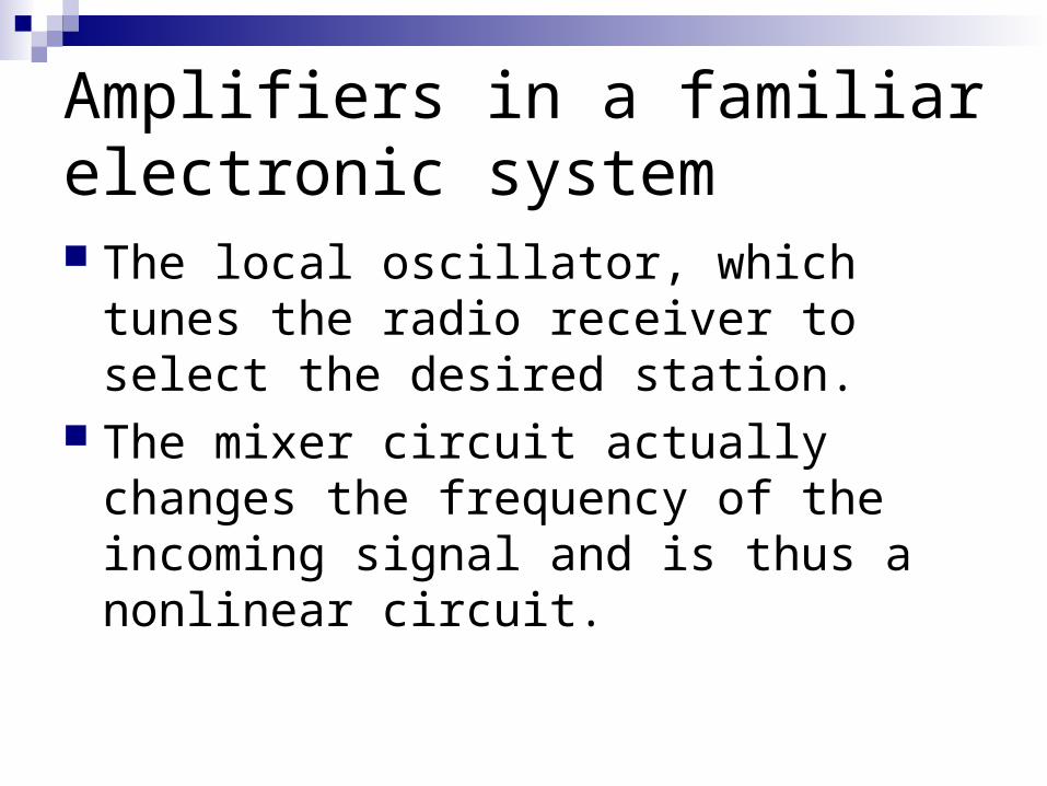
Amplifiers in a familiar electronic system The local oscillator, which tunes the radio
receiver to select the desired station. The mixer circuit actually changes the
frequency of the incoming signal and is thus a nonlinear circuit.

HW 1
1.2 1.11 1.20 1.22 1.48