JOHN BARDEEN and TRANSISTOR PHYSICS - The Chip History
17
“We were using gl[y]coborate as the electrolyte and izoticed an anodic oxide film growing on the surface of the germanium so we anodized the surface of a piece of germanium, washed off the glycoborate and evaporated the gold spots on it. As it turned out the germanium oxide was soluble in water and we had also washed it 081 So these experiments were done on a freshly anodized surface of germanium, and the first transistor was made on one of these samples anodized in this way! ’’ Nevertheless, Brattain continued experimenting on Dec. 15‘h with various combinations of voltage polarities on both the gold electrode and the point- contact electrode, the latter having been moved adjacent (just outside) the former electrode. One such combination had the gold electrode positively biased and the point-contact negatively biased, resulting in a voltage amplification of holes emitted from the gold electrode and collected at the point-contact (see 15- December entry in Table two); modulation was achieved by varying the potential of the emitting gold electrode. Bray has suggested Bardeen and Brattain might have utilized ac signals on both electrodes, with appropriate phases, (over and above the modulation effect at the emitter), thereby “explaining” their “selection” of the above choice of voltages and polarities that gave semiconductor amplification (transistor action) (41). In any case, the observed effect (with the gold electrode positively biased and the point contact negatively biased) was the opposite to what would have been expected if the oxide were present. In that case, a positive voltage applied to the gold electrode would have been expected to electrostatically induce electrons in the p- type inversion layer with a resultant decrease in the hole flow to the negatively biased point contact. Bardeen and Brattain had discovered “that it is possible to increase the conductivity by current flow from an appropriate contact on the germanium (31).” This was the first observation of semiconductor amplification (i.e., the transistor effect.) Although there was no power gain, there was a 2x voltage gain, independent of frequency up to lo4 Hz (23). Bardeen and Brattain concluded that the observed voltage gain was due to holes emitted from the positively-biased gold electrode into the germanium’s p-type inversion layer and collected at the negatively-biased collector. A signal applied between the emitter and the base electrode appeared in amplified form across a high- resistance load between the collector and the base (10). This observation resulted in the conception of the point-contact semiconductor amplifier and Bardeen and Brattain’s “035” patent disclosure (36) (see entry No. 4 in Table one). Michael Riordan and Lillian Hoddeson have noted that although Bardeen and Brattain failed to observe any power amplification with this configuration, Bardeen suggested a power gain should occur if two narrow contacts could be spaced only a few mils apart (23). Historic Day - December 16,1947 The Dec. 15Ih experiment quickly led to the experimental configuration utilized by Bardeen and Brattain on Dec. 16‘h, as shown in Figure 5. Specifically, Bardeen and Brattain utilized the same piece of germanium as used for the gold ring studies (Le., n-type polycrystalline germanium with a chemically induced p-type inversion layer) (10,ll). The germanium sample into which the plastic wedge pressed two stripes of gold foil is about half a centimeter long (42). The emitter was biased positively and emitted holes; the collector was biased negatively and collected the emitted holes. Both voltage and current amplification of an input signal, up to lo3 Hz with a power gain of about 2 dB, was achieved (see 16-December entry in Table two). One can clearly see the evaporated gold electrode in Figure 5 (from the Dec. 15Ih experiment) adjacent to the plastic wedge utilized for the definitive transistor experiment. Brattain has described how he achieved the point- contact separation - two parallel lines spaced about 50 pm apart - by cutting an evaporated strip of gold foil with a razor blade (43): “I accomplished it by getting my technical aide to cut me a polystyrene triangle which had a smart, narrow, flat edge and I cemented a piece of gold foil on it. After I got the gold on the triangle, very firmly, and dried, and we made contact to both ends of the gold, I took a razor and very carefully cut the gold in two at the apex of the triangle. 1 could tell when I had separated the gold. That’s all I did. I cut carefully with the razor until the circuit opened and put it on a spring and put it down on the same piece of germanium that had been anodized but standing around the room now for pretty near a week probably. I found that if1 wiggled it just right so that I had contact with both ends of the gold that I could make one contact an emitter and the other a collector, and that I had an amplifer with the order of magnitude of 100 amplification, clear up to the audio range.” 13
Transcript of JOHN BARDEEN and TRANSISTOR PHYSICS - The Chip History
“We were using gl[y]coborate as the electrolyte and izoticed an anodic oxide film growing on the surface of the germanium so we anodized the surface of a piece of germanium, washed off the glycoborate and evaporated the gold spots on it. As it turned out the germanium oxide was soluble in water and we had also washed it 081 So these experiments were done on a freshly anodized surface of germanium, and the first transistor was made on one of these samples anodized in this way! ’’
Nevertheless, Brattain continued experimenting on Dec. 15‘h with various combinations of voltage polarities on both the gold electrode and the point- contact electrode, the latter having been moved adjacent (just outside) the former electrode. One such combination had the gold electrode positively biased and the point-contact negatively biased, resulting in a voltage amplification of holes emitted from the gold electrode and collected at the point-contact (see 15- December entry in Table two); modulation was achieved by varying the potential of the emitting gold electrode. Bray has suggested Bardeen and Brattain might have utilized ac signals on both electrodes, with appropriate phases, (over and above the modulation effect at the emitter), thereby “explaining” their “selection” of the above choice of voltages and polarities that gave semiconductor amplification (transistor action) (41). In any case, the observed effect (with the gold electrode positively biased and the point contact negatively biased) was the opposite to what would have been expected if the oxide were present. In that case, a positive voltage applied to the gold electrode would have been expected to electrostatically induce electrons in the p- type inversion layer with a resultant decrease in the hole flow to the negatively biased point contact. Bardeen and Brattain had discovered “that it is possible to increase the conductivity by current flow from an appropriate contact on the germanium (31).” This was the first observation of semiconductor amplification (i.e., the transistor effect.) Although there was no power gain, there was a 2x voltage gain, independent of frequency up to lo4 Hz (23). Bardeen and Brattain concluded that the observed voltage gain was due to holes emitted from the positively-biased gold electrode into the germanium’s p-type inversion layer and collected at the negatively-biased collector. A signal applied between the emitter and the base electrode appeared in amplified form across a high- resistance load between the collector and the base (10). This observation resulted in the conception of the point-contact semiconductor amplifier and Bardeen and Brattain’s “035” patent disclosure (36)
(see entry No. 4 in Table one). Michael Riordan and Lillian Hoddeson have noted that although Bardeen and Brattain failed to observe any power amplification with this configuration, Bardeen suggested a power gain should occur if two narrow contacts could be spaced only a few mils apart (23).
Historic Day - December 16,1947
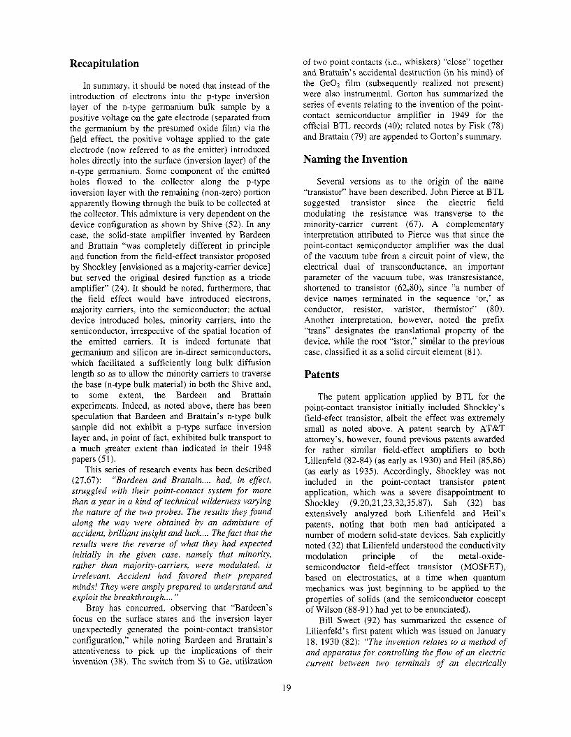
The Dec. 15Ih experiment quickly led to the experimental configuration utilized by Bardeen and Brattain on Dec. 16‘h, as shown in Figure 5. Specifically, Bardeen and Brattain utilized the same piece of germanium as used for the gold ring studies (Le., n-type polycrystalline germanium with a chemically induced p-type inversion layer) (10,ll). The germanium sample into which the plastic wedge pressed two stripes of gold foil is about half a centimeter long (42). The emitter was biased positively and emitted holes; the collector was biased negatively and collected the emitted holes. Both voltage and current amplification of an input signal, up to lo3 Hz with a power gain of about 2 dB, was achieved (see 16-December entry in Table two). One can clearly see the evaporated gold electrode in Figure 5 (from the Dec. 15Ih experiment) adjacent to the plastic wedge utilized for the definitive transistor experiment.
Brattain has described how he achieved the point- contact separation - two parallel lines spaced about 50 pm apart - by cutting an evaporated strip of gold foil with a razor blade (43): “I accomplished it by getting my technical aide to cut me a polystyrene triangle which had a smart, narrow, flat edge and I cemented a piece of gold foil on it. After I got the gold on the triangle, very firmly, and dried, and we made contact to both ends of the gold, I took a razor and very carefully cut the gold in two at the apex of the triangle. 1 could tell when I had separated the gold. That’s all I did. I cut carefully with the razor until the circuit opened and put it on a spring and put it down on the same piece of germanium that had been anodized but standing around the room now for pretty near a week probably. I found that if1 wiggled it just right so that I had contact with both ends of the gold that I could make one contact an emitter and the other a collector, and that I had an amplifer with the order of magnitude of 100 amplification, clear up to the audio range.”
13
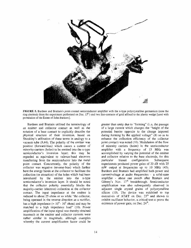
FIGURE 5. Bardeen and Brattain’s point-contact semiconductor amplifier with the n-type polycrystalline germanium (note the ring electrode from the experiment performed on Dec. 15Ih) and two line-contacts of gold affixed to the plastic wedge [used with permission of the Estate of John Bardeen].
Bardeen and Brattain utilized the terminology of an emitter and collector contact as well as the notation of a base contact to explicitly describe the physical structure of their invention, based on Shockley’s utilization of these terms in analogy to a vacuum tube (9,44). The polarity of the emitter was positive (forward-bias) which causes a current of minority-carriers (holes) to be emitted into the n-type semiconductor’s inversion layer; this may be regarded as equivalent to valence-band electrons transferring from the semiconductor into the metal point contact. Concurrently, the polarity of the collector was negative (reverse-bias) which further bent the energy bands at the collector to facilitate the collection (or attraction) of the holes which had been introduced by the emitter into the n-type semiconductor’s inversion layer. It should be noted that the collector polarity essentially blocks the majority-carrier (electron) collection at the collector contact. The input impedance at the emitter is reduced to about 25 ohms or so while “the collector, being operated in the reverse direction as a rectifier, has a high impedance (= lo4 - lo5 ohms) and may be matched to a high impedance load” (10). Power amplification of the input signal was thereby obtained inasmuch as the emitter and collector currents were rather similar in magnitude, although examples whereby the current amplification factor could be
greater than unity due to “forming” (i..e, the passage of a large current which changes the “height of the potential barrier opposite to the change imposed during forming by the applied voltage” (8) so as to enhance the collection efficiency of the collector point contact) was noted (lo). Modulation of the flow of minority carriers (holes) in the semiconductor amplifier with a frequency of 15 MHz was accomplished by varying the potential of the emitter and collector relative to the base electrode, for this particular biased configuration. Subsequent experiments produced power gains of 20 dB with 25 mW output at frequencies up to 10 MHz (43). Bardeen and Brattain had amplified both power and currentholtage at audio frequencies - a solid-state amplifier - about one month after Brattain and Gibney’s Nov. 1 7‘h breakthrough. Semiconductor amplification was also subsequently observed in adjacent single crystal grains of polycrystalline silicon (10). The device was exhibited to top executives of AT&T on Dec. 23rd and shown to exhibit oscillator behavior, a critical test to prove the existence of power gain, on Dec. 24‘h.
14
Minority-Carrier Transport: Surface, Bulk or an Admixture?
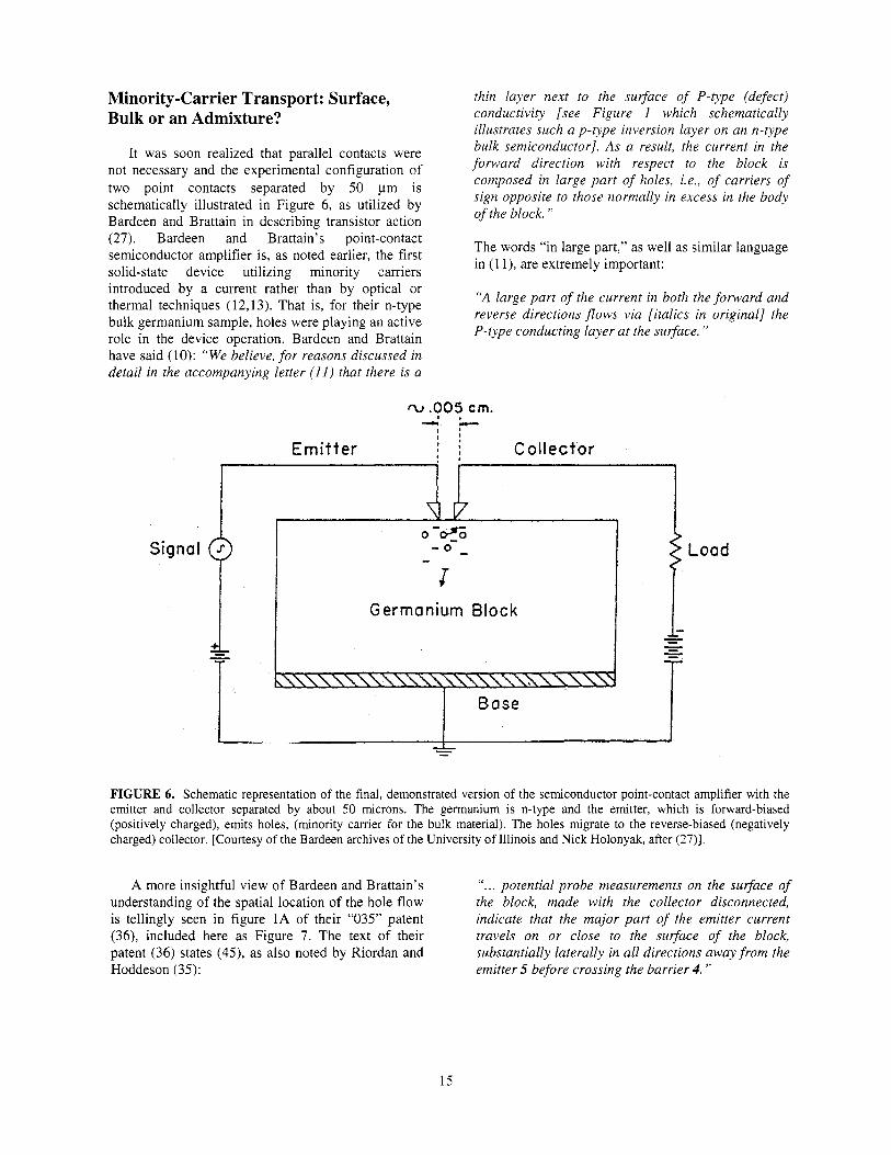
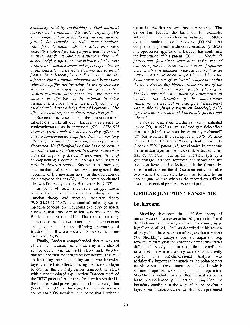
It was soon realized that parallel contacts were not necessary and the experimental configuration of two point contacts separated by 50 ym is schematically illustrated in Figure 6, as utilized by Bardeen and Brattain in describing transistor action (27). Bardeen and Brattain’s point-contact semiconductor amplifier is, as noted earlier, the first solid-state device utilizing minority carriers introduced by a current rather than by optical or thermal techniques (12,13). That is, for their n-type bulk germanium sample, holes were playing an active role in the device operation. Bardeen and Brattain have said (10): “We believe, for reasons discussed in detail in the accompanying letter (11) that there is a
thin layer next to the surface of P-type (defect) conductivity [see Figure 1 which schematically illustrates such a p-type inversion layer on an n-type bulk semiconductor]. As a result, the current in the forward direction with respect to the block is composed in large part of holes, i.e., of carriers of sign opposite to those normally in excess in the body of the block. ”
The words “in large part,” as well as similar language in (1 I ) , are extremely important:
“A large part of the current in both the forward and reverse directions flows via [italics in original] the P-type conducting layer at the surface. ’’
I ’
Emit te r Col lector
- T
Germanium Block
I Base
FIGURE 6. Schematic representation of the final, demonstrated version of the semiconductor point-contact amplifier with the emitter and collector separated by about 50 microns. The germanium is n-type and the emitter, which is forward-biased (positively charged), emits holes, (minority camer for the bulk material). The holes migrate to the reverse-biased (negatively charged) collector. [Courtesy of the Bardeen archives of the University of Illinois and Nick Holonyak, after (27 ) ] .
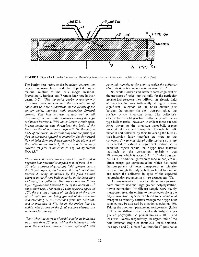
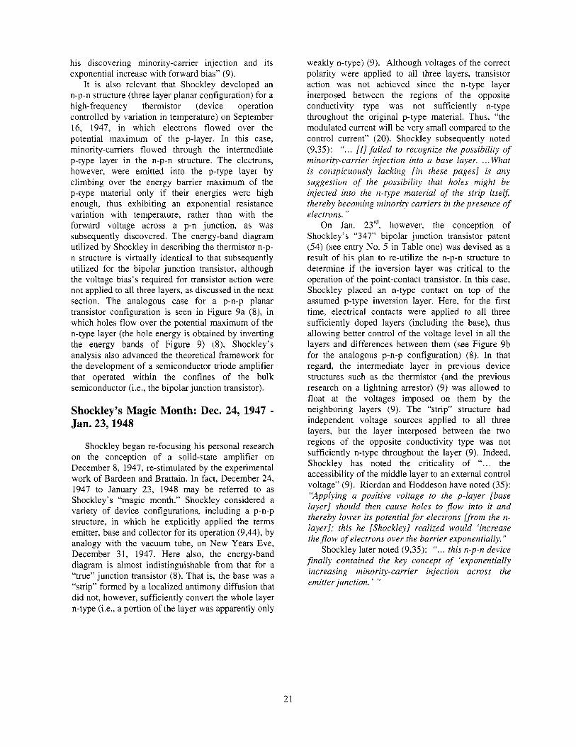
A more insightful view of Bardeen and Brattain’s I ‘ . . . potential probe measurements on the surface of understanding of the spatial location of the hole flow the block, made with the collector disconnected, is tellingly seen in figure 1A of their “035” patent indicate that the major part of the emitter current (36), included here as Figure 7. The text of their travels on or close to the surface of the block, patent (36) states (43 , as also noted by Riordan and substantially laterally in all directions away from the Hoddeson (35): emitter 5 before crossing the barrier 4.’’
15
‘2 N TYPE %e I t
FIGURE 7. Figure 1A from the Bardeen and Brattain point-contact semiconductor amplifier patent [after (36)].
The barrier here refers to the boundary between the p-type inversion layer and the depleted n-type material relative to the bulk n-type material. Interestingly, Bardeen and Brattain later note in their patent (46): “The potential probe measurements discussed above indicate that the concentration of holes, and thus the conductivity, in the vicinity of the emitter point, increase with increasing forward current. This hole current spreads out in all directions from the emitter 5 before crossing the high resistance barrier 4. With the collector circuit open, it then makes its way throughout the body of the block, to the plated lower surface 2. (In the N-type body of the block, the current may take the form of a flow of electrons upward to neutralize the downward flow of holes from the P-type layer.) In the absence of the collector electrode 6, this current is the only current. Its path is indicated in Fig. l a by stream lines 13. ’’
“Now when the collector 6 contact is made, and a negative bias potential is applied to it, of from -5 to - 50 volts, a strong electrostatic field appears across the P-type layer 3, and across the high resistance barrier 4, being maintained by the fixed positive charges in the N-type body material in the immediate vicinity of the collector. The barrier and the P-type layer together are believed to be of the order of cm in thickness. Thus with 10 volts across a space of
the average strength of this field is of the order of Id volts per cm, being greatest at the collector and extending in all directions from the collector, and is indicated in Fig. l a by the broken line 14, within which some of the fixed positive charges are indicated by plus signs.”
“Now when the current of positive holes as indicated by stream lines 15 comes within the influence of this field, the holes are attracted to the region of lowest
potential, namely, to the point at which the collector electrode 6 makes contact with the layer 3 . . . . ”
So, while Bardeen and Brattain were cognizant of the transport of holes into the bulk, for the particular geometrical structure they utilized, the electric field at the collector was sufficiently strong to ensure significant collection of the holes emitted just beneath the emitter via their transport along the surface p-type inversion layer. The collector’s electric field could penetrate sufficiently into the n- type bulk material, however, to collect those emitted holes traversing the inversion layer-bulk n-type material interface and transported through the bulk material and collected by their traversing the bulk n- type-inversion layer interface en route to the collector. The reverse-biased collector-base structure is expected to exhibit a significant portion of its depletion region within the n-type base material inasmuch as the germanium resistivity was 10 ohm-cm, which is about 1.3 x 10¹⁴ electrons per cm3 (47). In addition, germanium (and silicon) are in- direct energy-gap semiconductors which facilitated the component of holes transported as minority carriers through the n-type bulk material to survive and reach the collector, in spite of the expected recombination processes in n-type germanium (48).
An assessment as to whether the minority-carrier holes emitted into the large grained polycrystalline, n-type germanium (or silicon) sample were mainly transported from the emitter to the collector along the p-type inversion layer or exhibited some non-trivial transport as minority carriers through the n-type bulk sample, may be assessed by a model calculation (49). Taking the room-temperature minority-carrier (hole) lifetime and diffusion coefficient in the n-type, large- grained polycrystalline germanium as = 10 ,us and 49 cm2/s (48,50), respectively, an upper limit of the hole diffusion length of about 225 pm is obtained, (see eqs. 6 and 7), almost five times the 50 pm spatial
16
separation between the emitter and collector gold contact metal tips (10) (probe separations as much as 250 pm were also utilized).
where k is Boltzmann’s constant, T is the absolute temperature and q is the absolute value of the electronic charge.
Even if the two probes were placed in adjacent polycrystalline grains and the hole lifetime and diffusion coefficient were reduced, as a result of intergranular scattering, to = 1 ps and 12 cm2/s (48), respectively, the resulting diffusion length of about 35 pm would still be comparable to the probe separation of 50 pm. One might, therefore, anticipate some fraction of bulk minority-carrier transport, concurrent with transport in the inversion layer. In other words, the holes introduced at the emitter could flow as minority carriers, relative to the reverse- biased collector contact, either along the inversion layer or through the n-type bulk material as noted above. In that regard, there has been speculation that Bardeen and Brattain’s n-type bulk sample did not exhibit a p-type surface inversion layer and, in point of fact, exhibited a component of hole flow through the bulk of the n-type germanium to a much greater extent than indicated in their 1948 papers (51). Further complicating this retrospective analysis is Shockley’s recollection of a “most trying week somewhere in late Dec. [1947] or early Jan. [1948]
when for some reason the [surface] treatments failed and no transistors worked’ (20).
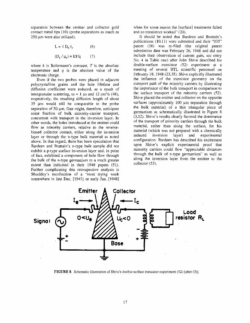
It should be noted that Bardeen and Brattain’s publications (10,l l) were submitted and their “035” patent (36) was re-filed (the original patent submission date was February 26, 1948 and did not include their observation of current gain, see entry No. 4 in Table one) after John Shive described his double-surface transistor (52) experiment at a meeting of several BTL scientific personnel on February 18, 1948 (23,35). Shive explicitly illustrated the influence of the transistor geometry on the transport path of the minority carriers by illustrating the importance of the bulk transport in comparison to the surface transport of the minority carriers (52). Shive placed the emitter and collector on the opposite surfaces (approximately 100 pm separation through the bulk material) of a thin triangular piece of germanium as schematically illustrated in Figure 8 (3,52). Shive’s results clearly favored the dominance of the transport of minority carriers through the bulk material, rather than along the surface, for his material (which was not prepared with a chemically induced inversion layer) and experimental configuration. Bardeen has described his excitement upon Shive’s explicit experimental proof that minority carriers could flow “appreciable distances through the bulk of n-type germanium” as well as along the inversion layer from the emitter to the collector (53).
Emitter A Collector
Signal toad
res i stor
FIGURE 8. Schematic illustration of Shive’s double-surface transistor experiment ( 5 2 ) [after (3)J.
17
It was during this meeting that Shockley presented his seminal contributions of minority- carrier injection over a barrier (named subsequent to the meeting), p-n junction theory and junction transistor theory (8,22,54), based on research entered into his notebook during January, 1948 (23). The injection concept refers to the transfer of majority carriers across a forward-biased p-n (or n-p) junction which facilitated their introduction into the adjacent material where, as minority carriers, they co-existed with the majority carriers and were transported, with an efficiency less than loo%, to an external circuit through the collector. Indeed, Shockley’s “488” injection patent (55 ) was filed on September 24, 1948 (later than the transistor patents) and was awarded on April 4, 1950 (earlier than the transistor patents), attesting to the importance (and recognition) of the concept (56). Shive’s experiment clearly illustrated the importance of the geometrical configuration in determining the extent of bulk transport (see Figure 8) (332) while Shockley’s p-n junction theory and junction transistor theory, originally a notebook account not shared with Bardeen or Brattain, facilitated the mathematical description of their previously disclosed semiconductor amplification (transistor action) (10,11,36) by using a one- dimensional analysis (8,22,54). Indeed, Shockley developed an early version of his junction approach on New Year’s Eve, 1947, subsequently witnessed by Morgan on Jan. 6, 1948 and Bardeen on Jan. gth, although there was no indication of minority-carrier injection in these notes (35). The injection concept was explicitly entered by Shockley in his notebook on Jan. 231d and witnessed by Dick Haynes on Jan. 27‘h (35). The injection phenomenon was experimentally identified by Haynes and Shockley in July, 1948 by measuring the hole mobility in n-type polycrystalline germanium (57).
During the next several years, clarification of a number of issues associated with the point-contact semiconductor amplifier ensued. These included the role of forming to ensure sufficient rectifying barriers (8,105859); the behavior of surface states at low- temperatures, wherein a larger field-effect was observed on an evaporated film of silicon since the release time of the electrons trapped in the surface states was longer than at room temperature for the given modulating electric field (59); the implications of an internal electric field at the surface of a semiconductor at thermal equilibrium (60-62); and quantitative expressions for the characterization of the SSCR and surface potential (63-66).
Contemporaneous Events
Contemporaneous with these events, relevant research on silicon and germanium was also in progress by Fred Seitz and his associates at the University of Pennsylvania, Harper North at the General Electric Company and several other research institutes (27,48,67,68). Seitz was developing purification methodologies for Si in the early ‘40s which facilitated the fabrication of high back-voltage rectifiers. The research at Purdue University under the direction of Lark-Horovitz (69-7 1) between 1942- 1945, however, must explicitly be noted inasmuch as Bray, a member of the Purdue team had, in retrospect, also observed minority-carrier injection (24,25,38,72-75), explicitly demonstrated by Shockley (8,2334-57). Bray suggested that the decreased resistivity in spreading resistance point- contact measurements (local resistivity near a point contact) on n-type germanium was due to electric- field enhanced effects in high fields; Bray also observed the bulk resistivity was reduced by high- voltage pulses. After the Bardeen and Brattain papers were published (10,11), Bray realized that his studies could be explained “by the production of holes” (35,71). The high-electric field effect was subsequently shown by Robert Ryder and Shockley to be due to the introduction of holes from the contacting terminals (76).
The Bell Laboratory personnel were quite apprehensive as regards the Purdue studies (77), as has been noted by Riordan and Hoddeson (35): “ ... Brattain found himself in an awkward position when he heard Seymour Benzer, another member of the Purdue group, mention the spreading resistance in late January 1948 at the New York American Physical Society meeting. He [Brattain] understood by then why the resistivity was decreasing near the point -that it was the result of hole emission at the point. Brattain recalled listening quietly to Benzer in the corridor, until Benzer remarked, “I think if somebody put another point contact down on the surface, close to this point, and measured the distribution of potential around the point, then we might be able to understand what this [effect] is about.” To that Brattain replied, “Yes, I think maybe that would be a very good experiment” and walked away.”
In that regard, Bray has retrospectively noted (24,25): “Bell people, knowing about our work, and how accidental was their own discovery, were fearful that we too might stumble upon the transistor and beat them to the priority of publication. ’’
18
Recapitulation
In summary, it should be noted that instead of the introduction of electrons into the p-type inversion layer of the n-type germanium bulk sample by a positive voltage on the gate electrode (separated from the germanium by the presumed oxide film) via the field effect, the positive voltage applied to the gate electrode (now referred to as the emitter) introduced holes directly into the surface (inversion layer) of the n-type germanium. Some component of the emitted holes flowed to the collector along the p-type inversion layer with the remaining (non-zero) portion apparently flowing through the bulk to be collected at the collector. This admixture is very dependent on the device configuration as shown by Shive (52). In any case, the solid-state amplifier invented by Bardeen and Brattain “was completely different in principle and function from the field-effect transistor proposed by Shockley [envisioned as a majority-carrier device] but served the original desired function as a triode amplifier” (24). It should be noted, furthermore, that the field effect would have introduced electrons, majority carriers, into the semiconductor; the actual device introduced holes, minority carriers, into the semiconductor, irrespective of the spatial location of the emitted carriers. It is indeed fortunate that germanium and silicon are in-direct semiconductors, which facilitated a sufficiently long bulk diffusion length so as to allow the minority carriers to traverse the base (n-type bulk material) in both the Shive and, to some extent, the Bardeen and Brattain experiments. Indeed, as noted above, there has been speculation that Bardeen and Brattain’s n-type bulk sample did not exhibit a p-type surface inversion layer and, in point of fact, exhibited bulk transport to a much greater extent than indicated in their 1948 papers (51).
This series of research events has been described (27,67): “Bardeen and Brattain .... had, in effect, struggled with their point-contact system for more than a year in a kind of technical wilderness valying the nature of the two probes. The results they found along the way were obtained by an admixture of accident, brilliant insight and luck .... The fact that the results were the reverse of what they had expected initially in the given case, namely that minority, rather than majority-carriers, were modulated, is irrelevant. Accident had favored their prepared minds! They were amply prepared to understand and exploit the breakthrough .... ’’
Bray has concurred, observing that “Bardeen’s focus on the surface states and the inversion layer unexpectedly generated the point-contact transistor configuration,” while noting Bardeen and Brattain’s attentiveness to pick up the implications of their invention (38). The switch from Si to Ge, utilization
of two point contacts (i.e., whiskers) “close” together and Brattain’s accidental destruction (in his mind) of the GeOz film (subsequently realized not present) were also instrumental. Gorton has summarized the series of events relating to the invention of the point- contact semiconductor amplifier in 1949 for the official BTL records (40); related notes by Fisk (78) and Brattain (79) are appended to Gorton’s summary.
Naming the Invention
Several versions as to the origin of the name “transistor” have been described. John Pierce at BTL suggested transistor since the electric field modulating the resistance was transverse to the minority-carrier current (67). A complementary interpretation attributed to Pierce was that since the point-contact semiconductor amplifier was the dual of the vacuum tube from a circuit point of view, the electrical dual of transconductance, an important parameter of the vacuum tube, was transresistance, shortened to transistor (62,80), since “a number of device names terminated in the sequence ‘or,’ as conductor, resistor, varistor, thermistor” (80). Another interpretation, however, noted the prefix “trans” designates the translational property of the device, while the root “istor,” similar to the previous case, classified it as a solid circuit element (81).
Patents
The patent application applied by BTL for the point-contact transistor initially included Shockley’s field-efect transistor, albeit the effect was extremely small as noted above. A patent search by AT&T attorney’s, however, found previous patents awarded for rather similar field-effect amplifiers to both Lillenfeld (82-84) (as early as 1930) and Heil (85,86) (as early as 1935). Accordingly, Shockley was not included in the point-contact transistor patent application, which was a severe disappointment to Shockley (9,20,21,23,32,35,87). Sah (32) has extensively analyzed both Lilienfeld and Heil’s patents, noting that both men had anticipated a number of modern solid-state devices. Sah explicitly noted (32) that Lilienfeld understood the conductivity modulation principle of the metal-oxide- semiconductor field-effect transistor (MOSFET), based on electrostatics, at a time when quantum mechanics was just beginning to be applied to the properties of solids (and the semiconductor concept of Wilson (88-91) had yet to be enunciated).
Bill Sweet (92) has summarized the essence of Lilienfeld’s first patent which was issued on January 18, 1930 (82): “The invention relates to a method of and apparatus fo r controlling the flow of an electric current between two terminals of an electrically
19
conducting solid by establishing a third potential between said terminals; and is particularly adaptable to the amplification of oscillating currents such as prevail, for example, in radio communications. Heretofore, thermionic tubes or valves have been generally employed for this purpose; and the present invention has for its object to dispense entirely with devices relying upon the transmission of electrons through an evacuated space and especially to devices of this character wherein the electrons are given off from an incandescent filament. The invention has for a further object a simple, substantial and inexpensive relay or amplifier not involving the use of excessive voltages, and in which no filament or equivalent element is present. More particularly, the invention consists in affecting, as by suitable incoming oscillations, a current in an electrically conducting solid of such characteristics that said current will be affected by and respond to electrostatic changes. ”
Bardeen has also noted the importance of Lilienfeld’s work, although Bardeen’s reference to semiconductors was in retrospect (92): “Lilienfeld deserves great credit f o r his pioneering efforts to make a semiconductor amplifier. This was not long after copper oxide and copper sulfide rectifiers were discovered. He [Lilienfeld] had the basic concept of controlling the flow of current in a semiconductor to make an amplibing device. It took many years of development of theory and materials technology to make his dream a reality.” Sah has noted, however, that neither Lilienfeld nor Heil recognized the necessity of the inversion layer for the operation of their proposed devices (32): “The inversion channel idea was first recognized by Bardeen in 1947 (32).”
In point of fact, Shockley’s disappointment became the major impetus for his subsequent p-n junction theory and junction transistor theory (9,20,2 1,23,32,35,87) and seminal minority-carrier injection concept (55). It should explicitly be noted, however, that transistor action was discovered by Bardeen and Brattain (42). The role of minority carriers and the first two transistors - point-contact and junction - and the differing approaches of Bardeen and Brattain vis-&vis Shockley has been discussed (23,35).
Finally, Bardeen comprehended that it was not efficient to modulate the conductivity of a slab of semiconductor via the field effect and, thereby, patented the first modern transistor device. This was an insulating gate modulating an n-type inversion layer via the field effect, utilizing the inversion layer to confine the minority-carrier transport, in series with a reverse-biased n-p junction. Bardeen received the “033” patent (29) for the effect, which resulted in the first recorded power gain in a solid-state amplifier (29-31). Sah (32) has described Bardeen’s device as a sourceless MOS transistor and noted that Bardeen’s
patent is “the first modern transistor patent ...” The device has become the basis of, for example, subsequent metal-oxide-semiconductor (MOS) dynamic random access memory (DRAM) and complementary-metal-oxide-semiconductor (CMOS) microprocessor applications. Bardeen has confirmed the importance of his patent (92): “ ... Nearly all present-day field-effect transistors make use of controlling the flow in an inversion layer of opposite conductivity o p e adjacent to the suface (such as an n-type inversion layer on p-@pe silicon.) I have the basic patent on use of an inversion layer to confine the jlow. Present-day bipolar transistors are of the junction type and are based on a patented structure Shockley invented while planning experiments to elucidate the dynamics of the point-contact transistor. The Bell Laboratories patent department was unable to obtain a patent on Shockley’s field- effect invention because of Lilienfeld’s patents and others. ’’
Shockley described Bardeen’s “033” patented device (29) in 1973 as “an insulated gate field-effect transistor (IGFET) with an inversion layer channel” (20) but re-canted this description in 1976 (9), since he noted that Bardeen’s “033” patent referred to Gibney’s “792” patent (33) for chemically preparing the inversion layer on the bulk semiconductor, rather than dynamically inducing the inversion layer by a gate voltage. Bardeen, however, had shown that the inversion layer in the device could be formed by either method (see the 8-December entry in Table two where the inversion layer was formed by an applied gate voltage whereas the other dates utilized a surface chemical preparation technique).
BIPOLAR JUNCTION TRANSISTOR
Background
Shockley developed the “diffusion theory of minority current to a reverse biased p-n junction” and the “behavior of minority electrons in a uniform p- layer” on April 24, 1947, as described in his review of the path to the conception of the junction transistor (9). Shockley’s analysis was an important step forward in clarifying the concept of minority-carrier diffusion in steady-state, non-equilibrium conditions in a medium where majority carriers concurrently existed. This one-dimensional analysis was additionally important inasmuch as the point-contact transistor was a three-dimensional device in which surface properties were integral to its operation. Shockley has noted, however, that his analysis of the large reverse-biased p-n junction, “simplified the boundary condition at the edge of the space-charge layer to zero minority-carrier density, but it prevented
20
his discovering minority-carrier injection and its exponential increase with forward bias” (9).
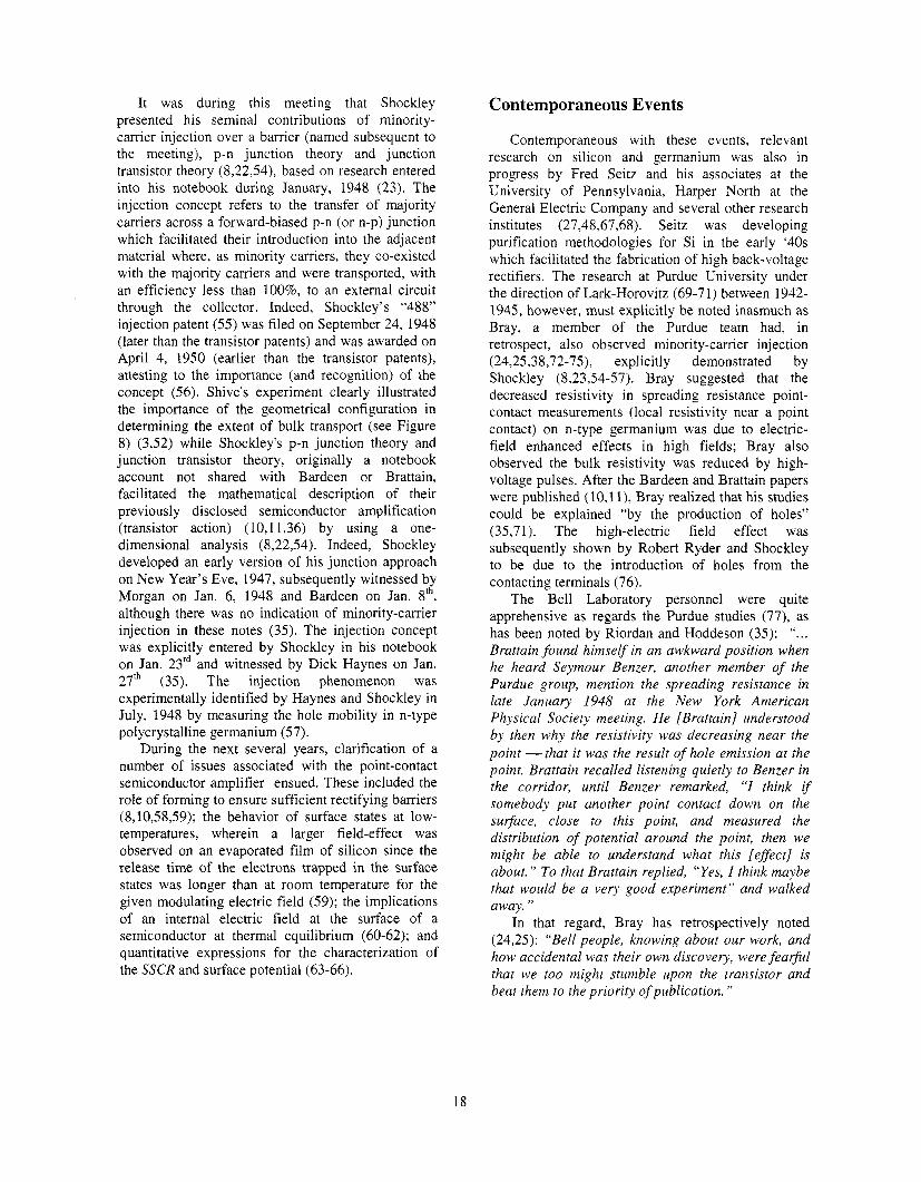
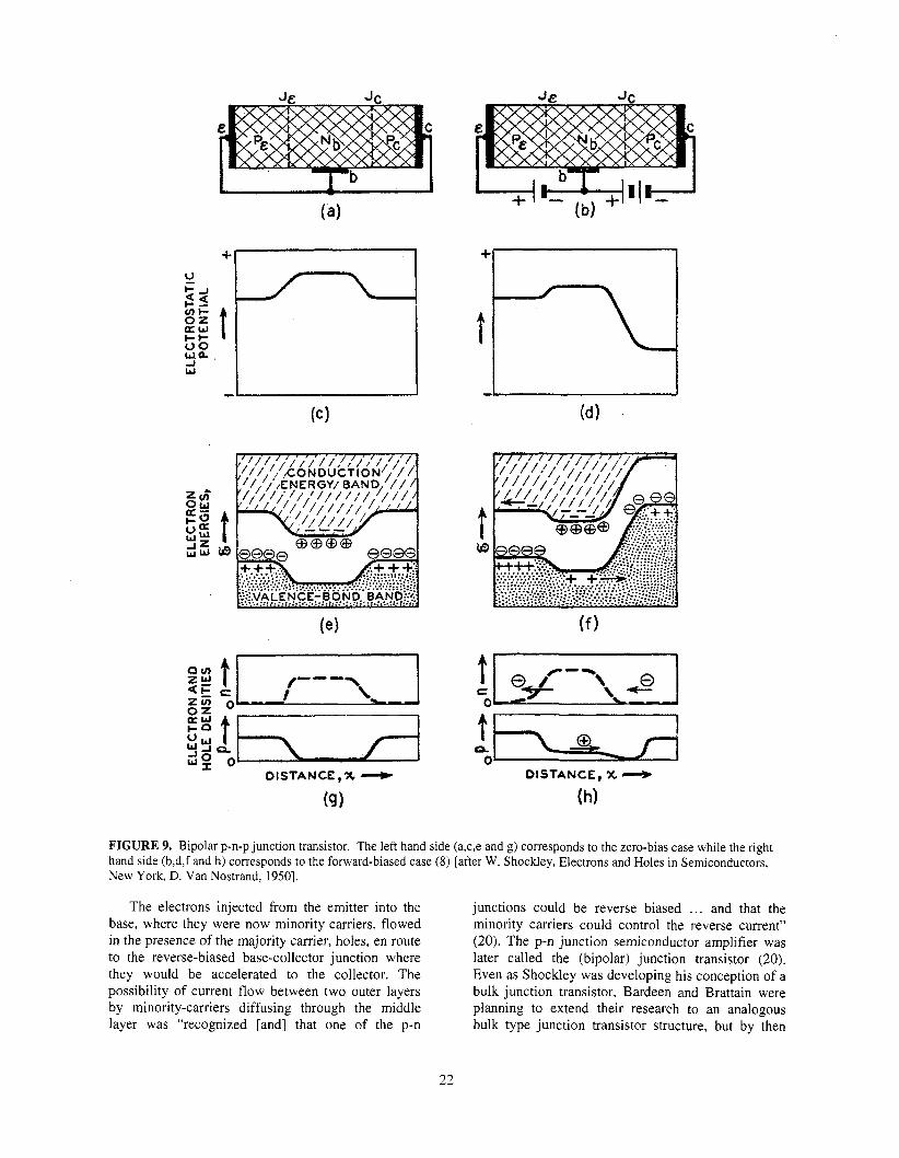
It is also relevant that Shockley developed an n-p-n structure (three layer planar configuration) for a high-frequency thermistor (device operation controlled by variation in temperature) on September 16, 1947, in which electrons flowed over the potential maximum of the p-layer. In this case, minority-carriers flowed through the intermediate p-type layer in the n-p-n structure. The electrons, however, were emitted into the p-type layer by climbing over the energy barrier maximum of the p-type material only if their energies were high enough, thus exhibiting an exponential resistance variation with temperature, rather than with the forward voltage across a p-n junction, as was subsequently discovered. The energy-band diagram utilized by Shockley in describing the thermistor n-p- n structure is virtually identical to that subsequently utilized for the bipolar junction transistor, although the voltage bias’s required for transistor action were not applied to all three layers, as discussed in the next section. The analogous case for a p-n-p planar transistor configuration is seen in Figure 9a (8), in which holes flow over the potential maximum of the n-type layer (the hole energy is obtained by inverting the energy bands of Figure 9) (8). Shockley’s analysis also advanced the theoretical framework for the development of a semiconductor triode amplifier that operated within the confines of the bulk semiconductor (Le., the bipolar junction transistor).
Shockley’s Magic Month: Dec. 24, 1947 - Jan. 23,1948
Shockley began re-focusing his personal research on the conception of a solid-state amplifier on December 8, 1947, re-stimulated by the experimental work of Bardeen and Brattain. In fact, December 24, 1947 to January 23, 1948 may be referred to as Shockley’s “magic month.” Shockley considered a variety of device configurations, including a p-n-p structure, in which he explicitly applied the terms emitter, base and collector for its operation (9,44), by analogy with the vacuum tube, on New Years Eve, December 31, 1947. Here also, the energy-band diagram is almost indistinguishable from that for a “true” junction transistor (8). That is, the base was a “strip” formed by a localized antimony diffusion that did not, however, sufficiently convert the whole layer n-type (i.e., a portion of the layer was apparently only
weakly n-type) (9). Although voltages of the correct polarity were applied to all three layers, transistor action was not achieved since the n-type layer interposed between the regions of the opposite conductivity type was not sufficiently n-type throughout the original p-type material. Thus, “the modulated current will be very small compared to the control current” (20). Shockley subsequently noted (9,35): I ‘ . . . [I] failed to recognize the possibility of minority-carrier injection into a base layer. . . . What is conspicuously lacking [in these pages] is any suggestion of the possibility that holes might be injected into the n-type material of the strip itse& thereby becoming minority carriers in the presence of electrons. ’’
On Jan. 231d, however, the conception of Shockley’s “347” bipolar junction transistor patent (54) (see entry No. 5 in Table one) was devised as a result of his plan to re-utilize the n-p-n structure to determine if the inversion layer was critical to the operation of the point-contact transistor. In this case, Shockley placed an n-type contact on top of the assumed p-type inversion layer. Here, for the first time, electrical contacts were applied to all three sufficiently doped layers (including the base), thus allowing better control of the voltage level in all the layers and differences between them (see Figure 9b for the analogous p-n-p configuration) (8). In that regard, the intermediate layer in previous device structures such as the thermistor (and the previous research on a lightning arrestor) (9) was allowed to float at the voltages imposed on them by the neighboring layers (9). The “strip” structure had independent voltage sources applied to all three layers, but the layer interposed between the two regions of the opposite conductivity type was not sufficiently n-type throughout the layer (9). Indeed, Shockley has noted the criticality of “ ... the accessibility of the middle layer to an external control voltage” (9). Riordan and Hoddeson have noted (35): “Applying a positive voltage to the p-layer [base layer] should then cause holes to flow into it and thereby lower its potential for electrons [from the n- layer]; this he [Shockley] realized would ‘increase the flow of electrons over the barrier exponentially.”
Shockley later noted (9,35): “... this n-p-n device finally contained the key concept of ‘exponentially increasing minority-carrier injection across the emitter junction. ’ ”
21
Jr JP
+7
A - OISTANCE, X ..--)
(g 1
+’
t
A-
DISTANCE, X r3
( h)
FIGURE 9. Bipolar p-n-p junction transistor. The left hand side (a,c,e and g) corresponds to the zero-bias case while the right hand side (b,d,f and h) corresponds to the forward-biased case (8) [after W. Shockley, Electrons and Holes in Semiconductors, New York, D. Van Nostrand, 19501.
The electrons injected from the emitter into the base, where they were now minority carriers, flowed in the presence of the majority carrier, holes, en route to the reverse-biased base-collector junction where they would be accelerated to the collector. The possibility of current flow between two outer layers by minority-carriers diffusing through the middle layer was “recognized [and] that one of the p-n
junctions could be reverse biased ... and that the minority carriers could control the reverse current” (20). The p-n junction semiconductor amplifier was later called the (bipolar) junction transistor (20). Even as Shockley was developing his conception of a bulk junction transistor, Bardeen and Brattain were planning to extend their research to an analogous bulk type junction transistor structure, but by then
22
Shockley had apparently covered these approaches in his research (23) and subsequent patent application (54).
It was now recognized that the three key concepts of the bipolar junction transistor involved: (a) minority-carrier injection over the potential barrier, which is exponentially reduced during forward bias at the emitter-base interface, as described in eq. 8 (8,9,22), (b) the high impedance at the base-collector interface developed as a result of the large reverse bias and (c) favorable geometry and doping levels to obtain good emitter to collector efficiency.
where I, is the saturation current, V is the applied bias, k is Boltzmann’s constant, T is the absolute temperature and q is the absolute value of the electronic charge. Since the minority carriers flowed in the presence of the dominant majority carriers in the base region, it was also recognized that the minority-carrier survival during transit in the base was strongly dependent on the properties of the semiconductor (48).
It should be noted, however, that Boris Davidov apparently had already suggested the importance of what we now call minority carriers in 1938 (87). Davidov had essentially derived eq. 8, obtained by Shockley a decade later, in his work explaining rectification (87), a major scientific challenge in the 1930’s. It has been suggested, though, that Davidov did not explicitly ensure the self-consistency of his analysis with the field equations (93). The success of the contemporaneous space-charge theory of rectification by Schottky (94-97), Mott (98,99), Davydov (100) and Bethe (101), also referred to as the “one current” theory of rectifiers, however, made further scientific discussion of minority carriers at the time moot (86). Riordan, Hoddeson and Conyers Herring, who are currently developing a more extensive analysis of Davydov’s work (102), have noted (87): “ ... the work of Boris Davydov on rectifying characteristics of semiconductors seems to have eluded notice until after the War, even though it was available in English-language publications (103,104). Working at the Ioffe Physico-Technical lnstitute in Leningrad, he [Davydov] came up with a model of rectification in copper oxide in 1938 that foreshadowed Shockley ’s work on p-n junctions more than a decade later. His idea involved the existence of a p-n junction in the oxide, with adjacent layers of excess and deficit semiconductor forming spontaneously due to an excess or deficit of copper relative to oxygen in the crystal lattice. Non- equilibrium concentrations of electrons and holes . . . could survive briefly in each other’s presence before
recombining. Using this model, Davydov successfully derived the current-voltage characteristics of copper- oxide rect$ers; his formula was essentially the same one that Shockley would derive a decade later for p-n junctions (22) . But his cumbersome mathematics and assumptions may have obscured the importance of his physical ideas to later workers. Bardeen, for example, was aware of Davydov’s publications by 1947 but does not seem to have recognized their significance until a few years later.”
Finally, as stated above, Bardeen has noted (92): “. . . Present day bipolar transistors are of the junction type and are based on a patented structure Shockley invented while planning experiments to elucidate the dynamics of the point-contact transistor.. ..” Nevertheless, the influence of an inversion layer on the performance of a two-junction structure without a gate was shown by Brown to be an important consideration in the junction structure’s performance (105).
The announcement of transistor action was made to the press on June 30, 1948 and reported on p.46 in “The News of Radio” section of the New York Times on July 1, 1948. Several key concepts, however, were developed after the invention of the junction theory transistor. These included the explicit demonstration of minority-carrier injection by Haynes and Shockley (57) and the reduction of the bulk resistance of n-type Ge due to hole injection by Ryder and Shockley (76).
Shockley’s “347” patent (54) was filed on June 26, 1948 and his extended p-n junction theory and junction transistor theory were published in 1949 (22). In the junction transistor, the emitter and collector of the point-contact transistor are replaced by two p-n planar junctions, one on either side of the n-type (or p-type) base material as in Figures 9a and 9b (8). Morgan Sparks and Robert Mikulyak presented an experimental “existence proof’ of a Ge p-n-p (non-colinear) transistor (with a power gain of 16) on April 7, 1949 (9). It was not until April, 1950, however, that p-n and n-p-n large area, planar junctions, grown by sequential single- and double- doping techniques during crystal growth, were fabricated (10-15 watts audio power I 20 KHz was achieved for the transistors), as part of Gordon Teal’s single-crystal research (with Ed Buehler and Morgan Sparks) (9,48). The microwatt n-p-n junction transistor was subsequently developed ( 106).
EVOLVING DIRECTIONS
The point-contact transistor was manufactured for ten years starting in 1951 by the Western Electric Division of AT&T (107). The apriori tuning of the point-contact transistor parameters, however, was not simple inasmuch as the device was very dependent on the detailed surface structure and, therefore, very
23
sensitive to humidity and temperature as well as exhibiting high noise levels. Accordingly, the devices differed significantly in their characteristics and electrical instabilities leading to “burnout” were not uncommon (108). With the implementation of crystalline materials in the early 1950’s (48,106,109), however, p-n junction transistors began replacing the point-contact transistor, silicon began replacing germanium (108) and the transfer of transistor technology from the lab to the fab accelerated (1 10- 112).
A major goal in the development of the point- contact semiconductor amplifier had been to replace the vacuum tube amplifier and electro-mechanical relay switch by a solid-state amplifier and switch, respectively. The achievement of higher power at higher frequencies was required. In point-of-fact, however, the small size of the transistor favored limited power-handling capabilities while the increased frequency response required small devices. It was recognized by Bob Wallace that chasing the vacuum tube led to the wrong emphasis. Rather, the opportunity was created by focusing on the transistor in its own right. The application of an invention is a powerful stimulus for innovation and development should not be restricted to the originally intended application as it may not be the most important. As attributed by Ian Ross to Wallace (107): “Gentlemen, you’ve got it all wrong! The advantage of the transistor is that it is inherently a small size and low-power device. This means that you can pack a large number of them in a small space without excessive heat generation and achieve low propagation delays. And that’s what we need for logic applications. The significance of the transistor is not that it can replace the tube but that it can do things the vacuum tube could never do!
SUMMARY
Semiconductor amplification (transistor action), with voltage, current and power gain, was experimentally observed by Bardeen and Brattain in n-type polycrystalline germanium on December 16, 1947 as a result of the judicious placement of gold- plated line contacts in nearby single crystal grains of the polycrystalline material. The date of the invention, however, has usually been taken as December 23, 1947 when the point-contact semiconductor amplifier and transistor action were demonstrated to top executives of Bell Telephone Laboratories (BTL). The first public demonstration of the invention and announcement of the discovery was not made until June 30, 1948, however, during which interval BTL rapidly expanded its research effort and developed its patent position. While Bardeen and Brattain noted that a large part of the current flowed
along the inversion layer as minority carriers from the emitter to the collector, there may also have been some non-trivial component of bulk transport from the emitter to the collector. In any case, Shive’s experiment clearly illustrated the importance of the geometrical configuration in determining the extent of bulk transport while Shockley’s seminal contribution of injection over a barrier, p-n junction theory and junction transistor theory facilitated the mathematical description of Bardeen and Brattain’s previously disclosed transistor action by using a one- dimensional analysis.
Bardeen also comprehended that it was not efficient to modulate the conductivity of a slab of semiconductor via the field effect and, thereby, developed his “033” patent (29), the first modern transistor device. This was an insulating gate modulating an n-type inversion layer via the field effect, utilizing the inversion layer to confine the minority-carrier transport, in series with a reverse- biased n-p junction, and resulted in the first recorded power gain in a solid-state amplifier. The device, described by Sah as a sourceless MOS transistor, became the basis of, for example, subsequent MOS memory DRAM and CMOS microprocessor applications.
Shockley placed great emphasis on the carrier injection and junction approach (8): “It seems likely that many inventions unforeseen at present will be made based on the principles of carrier injection, the field efsect, the Suhl effect, and the properties of rectihing junctions. It is quite probable that other new physical principles will also be utilized to practical ends as the art develops.”
On the other hand, Bardeen placed great emphasis on the role of the inversion layer, which as noted above, became the key ingredient in MOS memory DRAM and CMOS microprocessor applications. Shockley, moreover, has noted (1 13): “This book [Electrons and Holes in Semiconductors] had its origins in a series of lectures given at Bell Telephone Laboratories in connection with the growth of the transistor program. It thus owes its existence basically to the invention of the transistor by J. Bardeen and W.H. Brattain.”
Indeed, John Bardeen, the co-inventor of the point-contact transistor and inventor of the MOS transistor may rightly be called the father of modern electronics.
ACKNOWLEDGEMENTS
The author appreciates discussions with Professors Ralph Bray, H. Craig Casey, Jr., James Harris, Nick Holonyak, Jr., Michael Riordan, Frederick Seitz and Drs. Jim (James M.) Early and John L. Moll.
24
REFERENCES Conductors by Surface Charges, Phys. Rev., 74, 232-233 (1948)
1.
2.
3.
4.
5.
6.
7.
8.
9.
10.
11.
12.
13.
14.
L.S. Darken and R.W. Gurry, Physical Chemistry of Metals, New York, McGraw-Hill (1953)
R.A. Smith, Semiconductors, Cambridge, Cambridge University Press (1961)
E. Spenke, Electronic Semiconductors, New York, McGraw-Hill, (1958)
H.R. Huff, Semiconductors, Elemental Material Properties, Encyclopedia of Applied Physics., (G.L. Trigg, ed.), 17,437-475 (1996)
M.A. Green, Intrinsic Concentration, Effective Densities of States, and Effective Mass in Silicon, J. Appl. Phys., 67, 2944-2954 (1990)
A. Many, Y. Goldstein and N.B. Grover, Semiconductor Surfaces, New York, North- Holland ( 1965)
N. Holonyak, John Bardeen and The Point- Contact Transistor, Phys. Today, April, 36-43 (1992)
W. Shockley, Electrons and Holes in Semiconductors, New York, D.Van Nostrand (1 950)
W. Shockley, The Path to The Conception of The Junction Transistor, IEEE Trans. Electron Devices, ED-23, 597-620 (1976), reprinted in ED-31, 1523-1546 (1984)
J. Bardeen and W. H. Brattain, The Transistor, A SemiConductor Triode, Phys. Rev., 74, 230-23 1 (1948)
W.H. Brattain and J. Bardeen, Nature of The Forward Current in Germanium Point Contacts, Phys. Rev., 74,231-232 (1948)
B. Davydov, On The Photo-electromotive Force in Semiconductors, Tech. Phys. of USSR, 5,79-86 (1938)
B. Davydov, The Rectifying Action of Semiconductors, Tech. Phys. of USSR, 5, 87- 95 (1938)
W. Shockley and G.L. Pearson, Modulation of Conductance of Thin Films of Semi-
15.
16.
17.
18.
19.
20.
21.
22.
23.
24.
25.
26.
27.
J. Bardeen, Surface States and Rectification at a Metal Semi-Conductor Contact, Phys. Rev., 71, 717-727 (1947)
H.C. Torrey and C.A. Whitmer, Crystal Rectifiers, New York, McGraw-Hill(l948)
LE. Tamm, Uber Eine Mogliche Art der Elektronenbindung an Kristalloberflachen, Phys. Z. Sowjet, 1, 733-746 (1932)
I. E. Tamm, Z. Phys., 76,849 (1932)
W. Shockley, On The Surface States Associated With a Periodic Potential, Phys. Rev., 56,3 17-323 (1939)
W. Shockley, The Invention of The Transistor - “An Example of Creative-Failure Methodology,” National Bureau of Standards Special Publication 388, Proceedings on The Public Need and The Role of The Inventor, June 11-14, 1973, Monterey, Calif., 47-89 (1974), reprinted in Semiconductor Silicon/l998 (edited by H.R. Huff, U. Gosele and H. Tsuya), 26-68 (1998)
W. Shockley, 25 Years of Transistors, Bell Labs. Record, Dec., 340-341 (1972)
W. Shockley, The Theory of P-N Junctions in Semiconductors and P-N Junction Transistors, Bell Syst. Tech. J., 28, 435-489 (1949)
M. Riordan and L. Hoddeson, Crystal Fire, W.W. Norton, New York (1997)
R. Bray, The Invention of The Point-Contact Transistor: A Case Study in Serendipity, ULSI Science and Technology/l997 (edited by H.Z. Massoud, H. Iwai, C. Claeys and R.B. Fair), 37-50 (1997)
R. Bray, A Case Study in Serendipity, Interface, Spring, 24-3 1 (1997)
W.H. Brattain and R.B. Gibney, Three- Electrode Circuit Element Utilizing Semiconductor Materials, U.S. Patent No. 2,524,034, filed Feb. 26, 1948, issued Oct. 3, 1950
F. Seitz and N.G. Einspruch, The Tangled History of Silicon in Electronics,
25
Semiconductor Silicon / 1998, (edited by H.R. Huff, U. Gosele and H. Tsuya), 69-98 (1998)
40. W.S. Gorton, Memorandum For Record, A History of Engineering and Science in The Bell System (1925-1980), (edited by S. Millman), 97-100, Bell Telephone Laboratories (1983), (Brattain footnote added in 1975)
28.
29.
M. Riordan, private communication to H.R. Huff, (July 15, 1998)
J. Bardeen, Three-Electrode Circuit Element Utilizing Semiconductive Materials, U S . Patent No. 2,524,033, filed Feb. 26, 1948, issued Oct. 3, 1950
41.
42.
R. Bray, private communication to H.R. Huff, (Oct. 31, 1997)
M. Riordan, The Road to Silicon Was Paved With Germanium, Semiconductor Silicodl998 (edited by H.R. Huff, U. Gosele and H. Tsuya), 134- 142 (1998)
30. J. Bardeen, Semiconductor Research Leading to The Point Contact Transistor, Nobel Lecture, Dec. 11, 1956, Science, 126, 105-1 12 (1957)
C. Weiner, How The Transistor Emerged, IEEE Spectrum, Jan., 24-33 (1973)
43. 31.
32.
J. Bardeen, Solid State Physics - 1947, Solid State Technology, 30, 68-71, Dec., 1987
44. J. Bardeen, Notebook 20 780 entry, p. 72, 1946 C.T. Sah, Evolution of The MOS Transistor
-From Conception to VLSI, Proc. IEEE, 76, 1280-1326 (1988) 45.
46.
47.
See (36), column 10, lines 64-70
See (36), column 11, lines 10-24 33. R.B. Gibney, Electrolytic Surface Treatment of Germanium, U S . Patent No. 2,560,792, filed Feb. 26, 1948, issued July 17, 1951 S.M. Sze and J.C. Irvin, Resistivity, Mobility
and Impurity Levels in GaAs, Ge and Si at 300 K, Solid State Electron., 11, 599-602 (1968)
34. L. Hodesson, The Discovery of The Point- Contact Transistor, Historical Studies in the Physical Sciences, 12,41-76 (1981)
48. G.K. Teal, W.R. Runyan, K.E. Bean and H.R. Huff, Semiconductor Materials, (edited by J.F. Young and R.S. Shane), Materials and Processes, 3rd ed., 2 19-3 12, Marcel Dekker, New York (1985)
35. M. Riordan and L. Hoddeson, Minority Carriers and The First Two Transistors, Facets: New Perspectives on The History of Semiconductors, (edited by A. Goldstein and W. Aspray) 1-33 (1997), IEEE Press, New Brunswick. NJ 49.
50.
J. Harris, private communication to H.R. Huff (July 15,1998)
36. J. Bardeen and W.H. Brattain, Three- Electrode Circuit Element Utilizing Semiconductive Materials, U.S. Patent No. 2,524,035, filed June 17, 1948, issued Oct. 3, 1950
M.B. Prince, Drift Mobility in Semiconductors 1. Germanium, Phys. Rev., 92,681-687 (1953)
51.
52.
53.
G.L. Pearson, as noted by J. Harris, private communication to H.R. Huff (July 15, 1998) 37.
38.
39.
W.H. Brattain, Notebook 18 194 entry, December 4, 1947
J.N. Shive, The Double-Surface Transistor, Phys. Rev., 75,689-690 (1949) R. Bray presentation at SEMATECH, Austin,
TX, October 31, 1997 J. Bardeen, Three Men Who Changed Our World -. 25 Years Later, Bell Laboratories Record, Dec., 335-341 (1972)
W. Brattain, Discovery of The Transistor Effect: One Researcher’s Personal Account, Adventures in Experimental Phys., 5, 3-1 3 (1973) 54. W. Shockley, Semiconductor Amplifier
Patent, U.S. Patent No. 2,569,347, filed June 26, 1948, issued Sept., 25,1951
26
55. W. Shockley, Semiconductor Amplifier, U.S. Patent No. 2,502,488, filed Sept. 24,1948, issued April 4, 1950
From The History of Solid-State Physics, New York, Oxford University Presss (1992)
69. K. Lark-Horovitz, Preparation of Semiconductors and Development of Crystal Rectifiers, NDRC Report 14-585 (1946)
56.
57.
P.P. Bondyopadhyay, In The Beginning, Proc. IEEE, 86,63-77 (1998)
J.R. Haynes and W. Shockley, Investigation of Hole Injection in Transistor Action, Phys. Rev., 75, 691 (1949)
70.
71.
72.
K. Lark-Horovitz, AAAS, Washington, D.C. 57 (1954)
P.W. Henriksen, Solid State Physics Research at Purdue, Osiris, 2:3, 237-260 (1987) 58 . J. Bardeen and W.G. Pfann, Effects of
Electrical Forming on The Rectifying Barriers of n- and p-Germanium Transistors, Phys. Rev., 75,40 1-402 ( 1949)
R. Bray, K. Lark-Horovitz and R.N. Smith, Spreading Resistance Discrepancies and Field Effects in Germanium, Phys. Rev., 72, 530 ( 1947) J. Bardeen and W.H. Brattain, Physical
Principles Involved in Transistor Action, Phys. Rev., 75, 1208-1225 (1949)
59.
R. Bray, Dependence of Resistivity of Germanium on Electric Field, Phys. Rev., 74, 1218 (1948)
73.
60. G.L. Pearson and W.H. Brattain, History of Semiconductor Research, Proc. IRE, 43, 1794- 1806 (1955) 74. R. Bray, Dependence of Resistivity of
Germanium on Electric Field, Phys. Rev., 76, 152-153 (1949) 61. W.H. Brattain, Surface Properties of
Semiconductors, Science, 126, 15 1-155 ( 1957) 75.
76.
R. Bray, The Barrier Layer on P-Type Germanium, Phys. Rev., 76,458 (1949)
62.
63.
W.H. Brattain, Genesis of The Transistor, The Physics Teacher, March 109-1 14 (1968) J.R. Ryder and W. Shockley, Interpretation of
Dependence of Resistivity of Germanium on Electric Field, Phys. Rev., 75, 3 10 (1949) R.H. Kingston and S.F. Neustadter,
Calculation of the Space Charge, Electric Field and Free Carrier Concentration at The Surface of a Semiconductor, J. Appl. Phys., 26,718-720 (1955)
77. H.A. Zahl, Birth of The Transistor, The Microwave Journal, July, 94-96 (1966)
64. W.L. Brown, Surface Potential and Surface Charge Distribution from Semiconductor Field Effect Measurements, Phys. Rev., 100, 590-591 (1955)
78. J.B. Fisk, J.B. Fisk’s Letter to R. Brown, A History of Engineering and Science in The Bell System (1925-1980), (edited by S. Millman), 101, Bell Telephone Laboratories (1983)
65.
66.
67.
68.
C.G.B. Garrett and W.H. Brattain, Physical Theory of Semiconductor Surfaces, Phys. Rev., 99,376-387 (1955)
79. W.H. Brattain, W.H. Brattain’s Personal Reminiscences, Recorded by Brattain in 1975, A History of Engineering and Science in The Bell System (1925-1980), (edited by S. Millman), 101-102, Bell Telephone Laboratories (1983)
H.C. Montgomery and W.L. Brown, Field- Induced Conductivity Changes in Germanium, Phys. Rev., 103, 865-870 (1956)
80.
81.
J.R. Pierce, The Naming of The Transistor, Proc. IEEE, 86,37-45 (1998)
F. Seitz and N.G. Einspruch, Electronic Genie: The Tangled History of Silicon, Urbana, Il., Univ. of Illinois Press (1998)
J.A. Becker and J.N. Shive, The Transistor -A New Semiconductor Amplifier, Electrical Engineeering, 68, 215-221 (1949)
L. Hoddeson, E. Braun, J. Teichmann and S. Weart, Out of The Crystal Maze: Chapters
27
82. J.E. Lilienfeld, Method and Apparatus For Controlling Electric Currents, U S . Patent No. 1,745,175, Filed Oct. 8, 1926, Issued Jan. 18, 1930
96. W. Schottky, Zur Halbleitertheorie der Sperrschict-und Spitzengleichrichter, Z. Physik, 113, 367-414 (1939)
97.
98.
W. Schottky, Z. Physik, 118, 539-592 (1942) 83. J.E. Lilienfeld, Device For Controlling
Electric Current, U.S. Patent No. 1,900,018, Filed Mar. 28, 1928, Issued Mar. 7, 1933
N.F. Mott, Note on The Contact Between a Metal and an Insulator or Semiconductor, Proc. Cambridge Philos. SOC., 34,568-572 (1938) 84. J.E. Lilienfeld, Amplifier For Electric Current,
U.S. Patent No. 1,877,140, Filed Dec. 8, 1928, Issued Sept. 13, 1932 99.
100.
N.F. Mott, The Theory of Crystal Rectifiers, Proc. Roy. SOC. London A171,27-38 (1939)
85. 0. Heil, Improvements in or Relating to Electrical Amplifiers and Other Control Arrangements and Devices, Brit. Pat. No. 439,457, Filed Mar. 4, 1935, Issued Dec. 6, 1935
B. Davidov, On The Contact Resistance of Semiconductors, J. of Phys. (USSR), 1, 167- 174 (1939)
101.
102.
103.
H. Bethe, Theory of The Boundary Layer of Crystal Rectifiers, MIT Radiation Laboratory Report 43 (1942)
86. 0. Heil, Improvement in or Relating to Electrical Amplifiers and Other Control Arrangements and Devices, British Patent 439,457, September 26, 1939 C. Herring, M. Riordan and L. Hoddeson,
Boris Davydov's Theoretical Work on Minority Carriers, manuscript in preparation 87. M. Riordan, L. Hodesson and C. Herring, The
Invention of The Transistor, Rev. Modern Phys., 71, S336-S345 (1999) B. Davydov, On The Rectification of Current
at The Boundary Between Two Semi- Conductors, Compt. Rend. (Dokl.) Acad. Sci. URSS, 20,279-282 (1938)
88. A.H. Wilson, The Theory of Electronic Semi- Conductors, Proc. Roy. SOC., A133, 458-491 (1931)
104.
105.
106.
B. Davydov, On The Theory of Solid Rectifiers, Compt. Rend. (Dokl.) Acad. Sci. USSR, 20,283-285 (1938)
89. A.H. Wilson, The Theory of Electronic Semi- Conductors, Proc. Roy. SOC., A134, 277-287 (1931)
W.L. Brown, N-Type Surface Conductivity on P-Type Germanium, Phys. Rev., 91,518- 527 (1953)
90.
91.
92.
A.H. Wilson, Semiconductors and Metals, Cambridge Univ. Press (1939)
A.H. Wilson, The Theory of Metals, 2nd ed., Cambridge Univ. Press (1954)
W. Shockley, M. Sparkes and G.K. Teal, P-N Junction Transistors, Phys. Rev., 83, 151-162 (1951)
W. Sweet, American Physical Society Establishes Major Prize in Memory of Lilienfeld, Physics Today, May, 87-89 (1988)
107. I.M. Ross, The Invention of the Transistor, Proc. IEEE, 86, 7-28 ( 1998)
93.
94.
95.
J.L. Moll, private communication to H.R. Huff (March 2,2000) 108.
109.
LA. Ross, The Foundation of The Silicon Age, Physics Today, Dec., 34-39 (1997)
W. Schottky and E. Spenke, Wiss. Veroff. aus die Siemens Werken, 18 (3), 1-67 (1939) H.R. Huff, Twentieth Century Silicon
Microelectronics, ULSI Science and Technology/l997 (edited by H.Z. Massoud, H. Iwai, C. Claeys and R.B. Fair), 53-117 ( 1997)
W. Schottky, Semiconductor Theory of The Blocking Layer, Naturwiss, 26, 843 (1938) (in German)
28
110. H.R. Huff, manuscript in preparation 112. B.T. Murphy, D.E. Haggan and W.W. Troutman, From Circuit Miniaturization
11 1. to the Scalable IC, Proc. IEEE, 88, 691-703 J.L. Moll, Fifty Years of The Transistor: The
Symposium on VLSI Circuits, 5-8 (1997) Beginning of Silicon Technology, 1997 (2000)
113. W. Shockley, Electrons and Holes in Semiconductors, preface, New York, D. Van Nostrand (1950)
29