
Intelligent Ip Camera - Fpga Motion Detection Implementation

DEVELOPMENT OF A SMART CAMERA SYSTEM ON AN FPGA
by
Monica Jane Whitaker
A thesis submitted in partial fulfillmentof the requirements for the degree
of
Master of Science
in
Electrical Engineering
MONTANA STATE UNIVERSITYBozeman, Montana
November, 2016

c©COPYRIGHT
by
Monica Jane Whitaker
2016
All Rights Reserved

ii
ACKNOWLEDGEMENTS
I would like acknowledge the faculty and staff of the Electrical and
Computer Engineering Department as well as those of the Gianforte School
of Computing at Montana State University for their continued support and
encouragement throughout my undergraduate and graduate education.
Funding Acknowledgment
This work was kindly supported by the Montana Research and Economic
Development Initiative, Montana Board of Research and Commercialization
Technology and Resonon, Inc.

iii
TABLE OF CONTENTS
1. INTRODUCTION AND BACKGROUND......................................................1
Introduction .................................................................................................1Hyperspectral Imaging ..................................................................................3
Classifying a Hyperspectral Image.............................................................3Object Sorting ..............................................................................................4Smart Cameras .............................................................................................5Existing Smart Cameras ................................................................................6
Matrix Vision ..........................................................................................6Matrox Imaging .......................................................................................7Eye Vision Technology .............................................................................7Teledyne Dalsa ........................................................................................8The Winner is ... None of the Above .........................................................8
2. MOTIVATION ........................................................................................... 10
Beneficiaries ............................................................................................... 10Current Processing System .......................................................................... 11Why FPGA? .............................................................................................. 12
3. SYSTEM DESIGN...................................................................................... 15
Logistic Regression Algorithm...................................................................... 15Hardware Elements ..................................................................................... 17
Arria 10 SoC ......................................................................................... 17Development Board Components ............................................................ 18Additional Custom Boards ..................................................................... 18
Project Overview ........................................................................................ 20Camera Interface ................................................................................... 21DRAM Interface .................................................................................... 23Computation Unit.................................................................................. 25
Pixel Classification............................................................................ 25Object Classification ......................................................................... 27
FPGA Interface ..................................................................................... 28Performance .......................................................................................... 32

iv
TABLE OF CONTENTS - CONTINUED
4. IMPLEMENTATION DETAILS .................................................................. 33
Programmable Oscillator ............................................................................. 33Registers ............................................................................................... 33
Programmable Clock Generator ................................................................... 36Design Decisions .................................................................................... 36Registers ............................................................................................... 38Burning a Configuration ......................................................................... 38Utilizing the Clock Generator ................................................................. 39
Altera IP.................................................................................................... 39Timing Constraints ..................................................................................... 40Toolchain Fights ......................................................................................... 43
SignalTap .............................................................................................. 43TimeQuest Timing Analyzer................................................................... 44Chip Planner ......................................................................................... 44MATLAB.............................................................................................. 45
Toolchain Tricks ......................................................................................... 47
5. TEST AND VERIFICATION...................................................................... 50
Camera Interface ........................................................................................ 50DRAM ....................................................................................................... 50Computation Unit....................................................................................... 51FPGA to FPGA Transmission ..................................................................... 54
6. CONCLUSION........................................................................................... 56
REFERENCES CITED.................................................................................... 57
APPENDICES ................................................................................................ 60
APPENDIX A: Register Descriptions ........................................................ 61
APPENDIX B: VHDL Code ..................................................................... 65
APPENDIX C: MATLAB Code .............................................................. 141
v
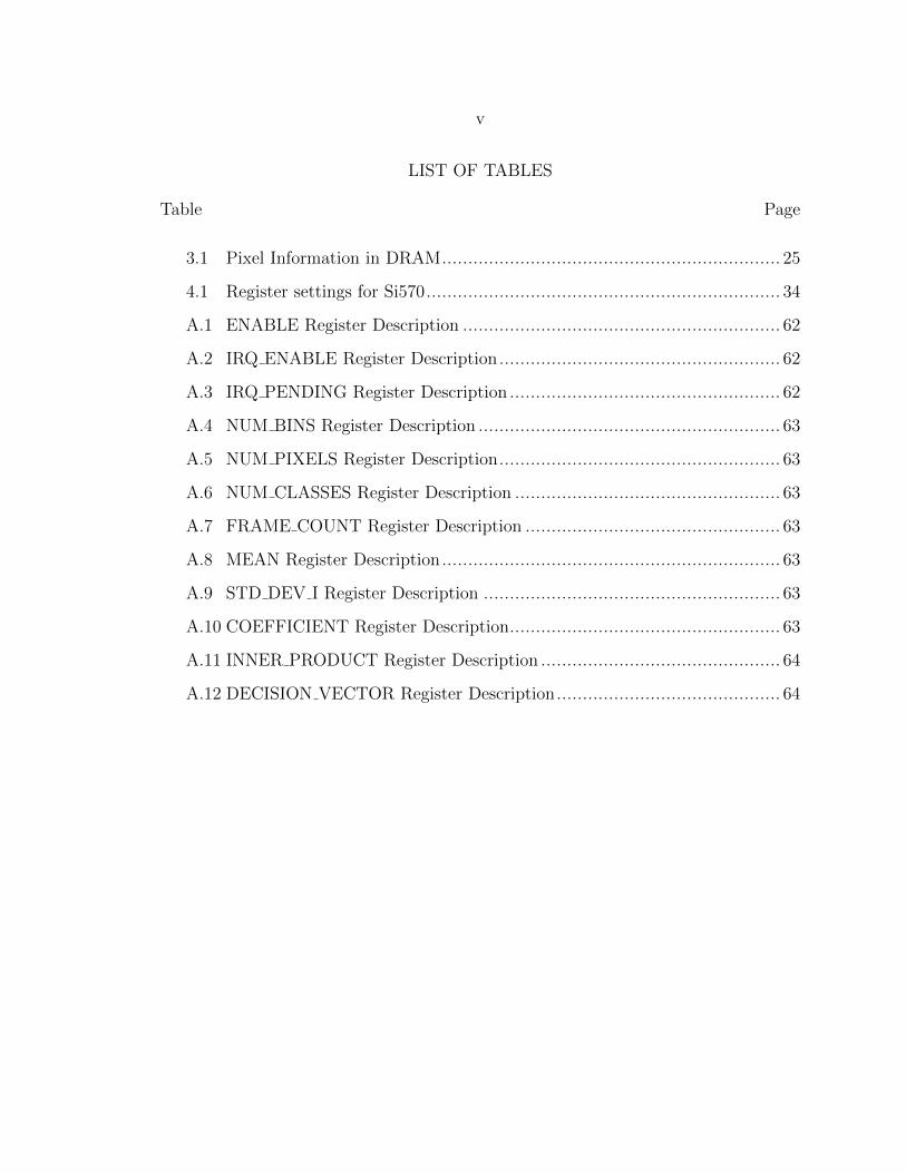
LIST OF TABLES
Table Page
3.1 Pixel Information in DRAM................................................................. 25
4.1 Register settings for Si570.................................................................... 34
A.1 ENABLE Register Description ............................................................. 62
A.2 IRQ ENABLE Register Description...................................................... 62
A.3 IRQ PENDING Register Description .................................................... 62
A.4 NUM BINS Register Description .......................................................... 63
A.5 NUM PIXELS Register Description...................................................... 63
A.6 NUM CLASSES Register Description ................................................... 63
A.7 FRAME COUNT Register Description ................................................. 63
A.8 MEAN Register Description................................................................. 63
A.9 STD DEV I Register Description ......................................................... 63
A.10 COEFFICIENT Register Description.................................................... 63
A.11 INNER PRODUCT Register Description .............................................. 64
A.12 DECISION VECTOR Register Description........................................... 64

vi
LIST OF FIGURES
Figure Page
1.1 A mock-up of the full system as it is intended to operate. ........................2
1.2 An example of hyperspectral line scan images over several frames.............4
1.3 Robot sorting almonds...........................................................................5
2.1 Depiction of a typical image processing system [1]. ................................ 11
2.2 This is a depiction of the future of image processing, with anintegrated camera sensor and FPGA processor [1]. ................................ 12
2.3 Graphical depiction of relative resources in the Arria 10 SoC chip .......... 14
3.1 Example inner product calculation. ...................................................... 16
3.2 High level view of the components external to the SoC utilizedin the system. The colored regions depict the individual PCBs............... 19
3.3 The PCBs created for the hyperspectral camera. ................................... 20
3.4 Block diagram of the full system functionality ....................................... 21
3.5 Block diagram of the camera interface subsystem. ................................. 22
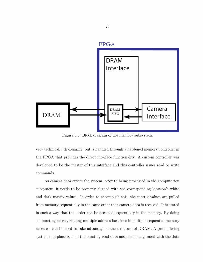
3.6 Block diagram of the memory subsystem. ............................................. 24
3.7 Block diagram of the computation subsystem........................................ 26
3.8 The connection between the Arria V development board (top)and the Arria 10 development board (bottom). ..................................... 29
4.1 Factory Default Clock Register Settings for Si570 .................................. 35
4.2 Preferred Clock Register Settings for Si570 ........................................... 35
4.3 Diagram of Pin Assignments for VersaClock 6 ProgrammableClock Generator .................................................................................. 37
4.4 A fitted floor plan in the Arria 10......................................................... 46
5.1 Generated plot depicting ratios between the pixels of the linescan camera and the pixels of the hyperspectral camera. ........................ 53
5.2 Zoomed in plot of ratios between monochrome and hyperspec-tral camera pixels ................................................................................ 53

vii
ABSTRACT
In recent years, hyperspectral cameras have been appearing in many applicationsthat need more information than what conventional color cameras can provide. Ahyperspectral camera is able to capture data ranging in wavelengths from the visiblespectrum all the way into the infrared. In this way, it is able to ’see’ hundreds of colors,much more than the human eye or any standard camera that typically uses only 3spectral values (corresponding to the standard red, green, and blue colors). Due tothe large amount of data that these cameras can generate at increasingly faster framerates, conventional computers are not able to perform all the necessary processing inreal-time. Because of this limitation, a new system is needed to perform the imageprocessing. This master’s thesis is meant to contribute to the development of a smartcamera targeted for hyperspectral image processing using a Field Programmable GateArray (FPGA) and object sorting with a prototype waterfall system. Through theuse of a Hardware Description Language (HDL), a currently used image processingalgorithm has been implemented to classify pixels. Additionally, design and testof an architecture for full object classification has been developed for the FPGA.High-speed transceivers are used to move data between multiple FPGA developmentboards. When paired with a hyperspectral camera and a monochrome line scancamera, this prototype system is capable of scanning objects in freefall and decidingwithin milliseconds whether or not to keep the object. This decision will dictate theaction of air jets to displace unwanted objects. This full system is potentially ofinterest to small businesses or farms as it will enable farmers to perform their ownpremium bulk sorting in a cost effective manner.

1
INTRODUCTION AND BACKGROUND
Introduction
A smart camera system is being developed to target sorting applications using a
hyperspectral camera. The overall system in development includes the hyperspectral
camera, a monochrome line scan camera and a sorting mechanism that uses air jets
to perform the physical sorting. This camera system will replace existing systems by
removing the need for cables between the camera and the processing unit as well as
replacing conveyor belts and robots with a vibrator feeder and air jets. In doing so,
with the help of the hyperspectral data, sorting may become more accurate and the
unit may end up being cheaper and consequently more accessible to small businesses.
This project is a prototype for the end result and is consequently not as compact as the
final product is anticipated to be, but it performs all the necessary calculations and
produces a result to trigger the air jets for the sorting of objects with high precision
due to the inclusion of hyperspectral data. This smart camera system utilizes two
System-on-Chip (SoC) devices that each consist of a Field Programmable Gate Array
(FPGA) fabric and a Hard Processor System (HPS) implemented on a single silicon
chip for easy and fast interactions. The fabric of these SoC FPGAs is used for the
processing of all data generated by the cameras, while the HPS is utilized in user
interactions and memory transfers. The monochrome line scan camera is included
for detection of the objects at the time of imaging and building an object profile
for the processing unit to make a complete object decision based on the compiled
individual pixel decisions. The decisions are made based on classes designed around
the hyperspectral characteristics found using the hyperspectral camera included in
this system.

2
Figure 1.1: A mock-up of the system as it is intended to operate. The productwill fall from the conveyor belt and be imaged by both cameras (one high resolutionmonochrome and one hyperspectral) simultaneously before either continuing its fallor being ejected by air jets.
This thesis focuses primarily on the development and implementation of the
image processing algorithm in addition to the interaction between development
boards. The air jet system is in development by a separate team of engineers, as
is the monochrome camera processing subsystem that identifies object boundaries
for the hyperspectral camera. In implementation of the prototype design for this
project, the author of this thesis is responsible for the development and testing of the
image processing algorithm for the hyperspectral camera data and the transceiver
communication between development boards. The author also worked with the
development tools to compile the whole project and fix timing errors. Additionally,

3
this author set up the data access method between the FPGA and the off-chip
Dynamic Random Access Memory (DRAM) connected directly to the FPGA fabric
via dedicated and hardened DRAM controllers. The details of this system are
abstracted away and a few control lines are available for use by other subsystems.
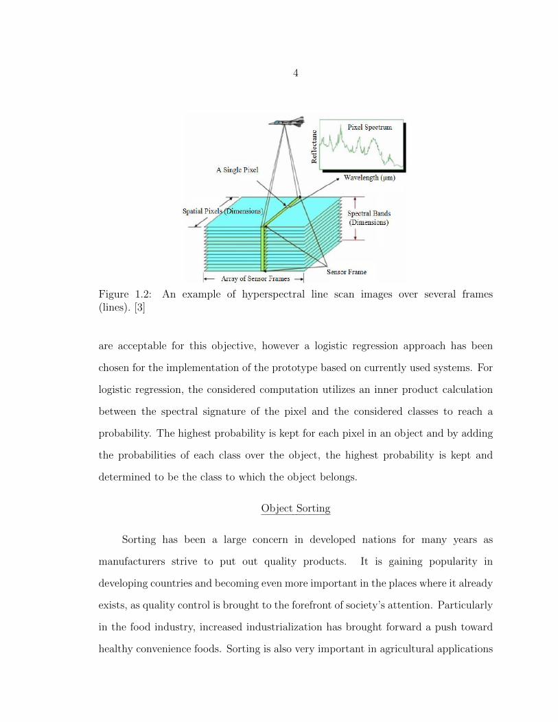
Hyperspectral Imaging
Resonon defines a hyperspectral image as a digital image with far more spectral
information for each pixel than traditional color cameras. The resulting data can
be pictured as a cube with dimensions in the spatial x and y directions and a third
dimension in the spectral wavelength, as seen in Figure 1.2. The cameras utilized in
the sorting applications explored within this thesis are line scan cameras, so a frame
consists of a single line (spatial y = 1) of pixels (spatial x) and then the spectral
bands occupying the ’third’ dimension. With the extra wavelength values, including
those in the infrared, hyperspectral cameras are able to sense much more information
than the human eye and your typical RGB color camera. This technology is used in
anything from remote sensing to quality control to sorting [2].
Classifying a Hyperspectral Image
Every pixel within an object contains nearly unique spectral signatures which
can be used to classify it. In order to do so, a class is defined by compiling a
variety of images of the object and determining the spectral signature that most
commonly defines the pixels within the object. This is done for each of the possible
classes expected to be seen in the surveyed objects. In this way, each class is a
vector of values across all the spectral bands. Using these classes, a statistically-
based machine learning algorithm is used in order to come up with a probability that
the pixel belongs to each class. A number of different machine learning algorithms
4
Figure 1.2: An example of hyperspectral line scan images over several frames(lines). [3]
are acceptable for this objective, however a logistic regression approach has been
chosen for the implementation of the prototype based on currently used systems. For
logistic regression, the considered computation utilizes an inner product calculation
between the spectral signature of the pixel and the considered classes to reach a
probability. The highest probability is kept for each pixel in an object and by adding
the probabilities of each class over the object, the highest probability is kept and
determined to be the class to which the object belongs.
Object Sorting
Sorting has been a large concern in developed nations for many years as
manufacturers strive to put out quality products. It is gaining popularity in
developing countries and becoming even more important in the places where it already
exists, as quality control is brought to the forefront of society’s attention. Particularly
in the food industry, increased industrialization has brought forward a push toward
healthy convenience foods. Sorting is also very important in agricultural applications

5
as farmers need to sort their crops after harvesting. In many cases, this is done by an
industrial company who then reports back with the percent loss due to the sorting
mechanism. Of course, by sending it away, farmers have no way of verifying the
reported loss and it would be easier and more reliable for them to have their own
means of sorting. Machine sorting helps to avoid the inconsistent nature of manual
sorting [4] and avoids significant loss of good product that may result from vibration
sorting or other mechanical means. Sorting machines come in a variety of shapes,
sizes, and technologies. These include using lasers, cameras, or x-ray in conjunction
with robotic arms or air jet systems to sort products and separate the bad from the
good [4]. As the technology advances, the sorting abilities will be expected to do so,
as well.
Figure 1.3: Robot sorting almonds [2]
Smart Cameras
In many applications, cameras of all varieties are used to acquire data for
studying something about the subject matter that can be viewed at a later time. This

6
data is also generally processed external to the system in which it abides. However, it
is becoming more necessary and common for processing to happen on-board, enabling
the system to adjust in real-time. Because of this, real-time processing is in high
demand and the techniques are still being perfected. Further, the algorithms to
process data generated by cameras are in constant refinement as researchers learn
what they want to see from the data and how best to achieve those results. As
algorithms are refined and cameras are built to generate more data than ever before, it
becomes necessary to have the right infrastructure to support the real-time processing
of imaging data, and thus we find the niche for a smart camera.
Existing Smart Cameras
There are several smart cameras currently in existence, including some with a
programmable FPGA or select-able image processing algorithms to utilize in the
desired application. These include several by Matrix Vision and some by other
companies such as Matrox Imaging, EVT, and Teldyne Dalsa as further described
in the following subsections. Though these cameras are likely very useful in
some applications which require on-board image processing, they lack the real-time
processing advantages gained in the use of the Arria 10 FPGA, which are detailed in
the last subsection below.
Matrix Vision
Matrix Vision has created several smart cameras, two of which are notable for
image processing in industry. The mvBlueGEMINI is touted as a ’Tool box technology
camera’ and includes an SoC with FPGA and Dual-Core Cortex-A9 with 800 MHz-
capable clocks and a camera sensor with 1280 x 1024 resolution. The software that

7
comes with the camera includes a Graphical User Interface (GUI) with which users
can choose the task to complete. The frame rate on this single sensor is unspecified. [5]
The other smart camera by Matrix Vision is the mvBlueLYNX-X. This camera
has options for either CCD or CMOS sensors in addition to a hybrid dual core. This
features a Cortex-A8 ARM CPU with a separate real-time Digital Signal Processing
(DSP) unit with video interface. The CPU has a clock speed up to 1 GHz, while the
DSP can run up to 800 MHz. Though available in a number of different resolutions,
the largest, 2592 x 1944 has a maximum frame rate of 14.4 Hz and the next largest,
1280 x 1024 has a maximum frame rate of 60 Hz. [6]
Matrox Imaging
Matrox makes a smart camera entitled the Iris GT which comes with a design
assistant and a web-based interface for the integrated development environment. This
camera has an Intel Atom embedded processor running Windows as well as a built-
in keyboard, monitor, and mouse for friendly user interface. It is compatible with
a variety of monochrome and color CCD sensors. Matrox claims this camera and
software are ideal for a variety of machine vision applications including agriculture,
aerospace, and more. The highest frame rate is 110 frames per second (fps), with an
effective resolution of 640 x 480. [7]
Eye Vision Technology
Eye Vision Technology (EVT) creates several variations of smart cameras. The
RazerCam, for instance, is packaged with a free programmable FPGA and two ARM
Cores based on the Xilinx Zynq SoC. Users are limited to choosing between one of
two matrix sensors or a line scan sensor with 4K resolution. That line sensor claims
a frame rate of 10000 fps with 10-bit pixel data, but the matrix sensors are not above
60 fps. The ARM cores are running Linux for user convenience in interaction. The

8
greatest downfall of this camera is the lack of hardened floating point on the FPGA,
which could hinder the speed or accuracy of results, not to mention development
speed. EVT also has a series of EyeCheck smart cameras which are almost all around
30 or 60 fps at resolutions in the thousands. One version has 180 fps and a Xilinx
Artix-7 FPGA with 28K logic elements. This FPGA is in the low-end of Xilinx’s
product portfolio, designed to optimize power and cost. [8]
Teledyne Dalsa
Teldyne Dalsa offers several vision systems with embedded software applications.
There are monochrome sensors available with resolution up to 1600 x 1200. The
processing includes an embedded CPU and DSP with a choice of software. These
are built robustly for integration in factory environments. These cameras are ideal
for still-image quality control and do not have the high clock rate possible with an
FPGA. [9]
The Winner is ... None of the Above
As seen here, there are many different options for smart cameras already on the
market that could be fitted with a hyperspectral front end and used for sorting objects.
But ultimately, none of these were chosen. This is because they lack what could be
known as the best combination of options. Some of these are outfitted with DSP
software and pre-programmed algorithms to choose from. Others use FPGAs for user
configurability. However, the DSP software is not all-encompassing and the FPGAs
more than likely do not have hardened floating point blocks. In the application
space targeted here, the hardened floating point is particularly valuable for ’cheaper’
calculations with greater accuracy. Further, by using only an FPGA to do all the
processing, any algorithm could be configured and used. Real-time processing also
greatly benefits from the deterministic latencies of FPGAs whereas other systems are

9
compromised by the inclusion of numerous memory accesses or operating systems.
Additionally, the sensors available for these cameras have frame rates less than 100
fps in most cases and the ideal sensor will be collecting data much faster than that.
For these reasons, it was decided that a new smart camera should be developed and
thus, this project was born.

10
MOTIVATION
Beneficiaries
This project is done in support of, and with support from, Resonon Inc. in
the belief that they will be able to utilize the smart camera in their machine vision
technology systems. Upon completion of a system prototype, of which this thesis
is a subsection, they could utilize the processing method and small form factor in
other integrated systems that they pair with their optical technology. Further, the
Montana Board of Research and Commercialization Technology helped to start the
work on this project and its first proof of concept iteration as they were providing
the primary source of funding for materials and man-hours spent developing this
technology implementation.
The primary focus for this smart camera implementation is in food sorting, but
the technology could be utilized in any sort of assembly-line environment requiring
quality assurance checks. Currently, in areas using the Resonon machine vision
technology, there is still the need for manual sorting after the machine has performed
its sorting because the current system is not capable of processing all the necessary
data at a sufficiently fast speed in order to make highly accurate classifications. Due
to the unavailability of a suitable image processing system, the images are lower
resolution than the Resonon optics technology is ultimately capable of in order to
allow processing to be done on a traditional PC. The goal of having an efficient
real-time integrated machine sorting system that is able to process high-resolution
images, is to eliminate the need for manual sorting after the machine which will free
up workers for other tasks. Using an FPGA enables a fully customizable smart camera
implementation that could apply in several application areas.

11
Current Processing System
A typical image processing system is shown in Figure 2.1. This system is
comprised of a camera, a frame grabber to configure and capture image data from
the camera, and a computer to perform the processing.
Figure 2.1: Depiction of a typical image processing system [1].
Though this method has worked for many years, it limits the speed at which
images can be processed due to several bottlenecks. The first bottleneck comes from
the cables that limit bandwidth. The second bottleneck is the speed of the computer
that limits the speed of real-time computations. The previous proof-of-concept system
utilized Camera Link connections to connect the camera to the FPGA. The Camera
Link standard was designed modeling the Channel Link technology, which is able to
transmit data at up to 2.38 Gbps [10]. With current applications of image processing,
the need for real-time results is growing and placing a strain on the capabilities of
existing systems. This project seeks to provide a solution for the replacement of these
traditional systems by integrating all three components as shown in Figure 2.2 and
removing the need for any cables. The proposed implementation involves short ribbon
cables to move data between the board housing the camera sensor and the FPGA
board. This is done so that the camera sensor can be easily placed at a 90◦ angle

12
to the board for this prototype. These ribbon cables will eventually be replaced by
board-edge connectors since the cables are not required for implementation purposes,
as far as the data movement is concerned and could easily be removed in a final
product.
Figure 2.2: This is a depiction of the future of image processing, with an integratedcamera sensor and FPGA processor [1].
Why FPGA?
One of the biggest advantages of FPGAs over standard computers is the
deterministic low-latency data paths achievable in custom application-specific archi-
tectures. CPUs have fixed architectures and variable latency depending on where
the data is stored or moved (cache, main memory, etc.). FPGAs are made of
programmable logic blocks, SRAM, and DSP blocks that can be reconfigured for
varying applications. The architecture of an FPGA is like a grid, with logic connected
over interconnects between blocks. Because of this structure, FPGAs have no
cache and a flexible architecture can be programmed by the user using a hardware
description language. In doing so, ultimate control is maintained over what occurs on
each clock cycle and even where each of the internal registers are placed to garner the
best path through the device. The deterministic latency is key for real-time systems

13
as the user is able to guarantee that the performance is real-time. Fabric is also easily
expanded by adding more logic blocks, which enables manufacturers to create similar
devices of varying size and complexity. In this way, FPGAs have been tailored to be
suitable for a whole market of people with varying needs, resources, and cost targets.
In this project two SoCs are used, instead of the standard FPGA that does not
include the ARM CPUs. A SoC contains a dual-core ARM processor on the same
chip as the FPGA along with hardened peripheral (Ethernet, USB, etc.), which is
referred to as a Hard Processor System (HPS). Providing an HPS that can serve
as a smart interface between the FPGA logic and the outside world makes it easier
to communicate with external computers for the passing of data. This is generally
accomplished using the Ethernet connection to achieve an IP address on the Linux
system running on the HPS. However, while the HPS is still functioning as a standard
computer and is subject to timing constraints applied by the OS scheduler, the
FPGA can continually be running and performing the computationally demanding
or timing specific tasks concurrently. It is able to send interrupts to the HPS and
the HPS can read or write to the memory available to the FPGA. A depiction of the
resources available and their relative locations within the Arria 10 SoC chip is shown
in Figure 2.3. The architecture of the Arria V SoC is similarly laid out, though with
lower-level technology in the transceivers and DSP blocks.

14
Figure 2.3: Graphical depiction of relative resources in the Arria 10 SoC chip [11]
15
SYSTEM DESIGN
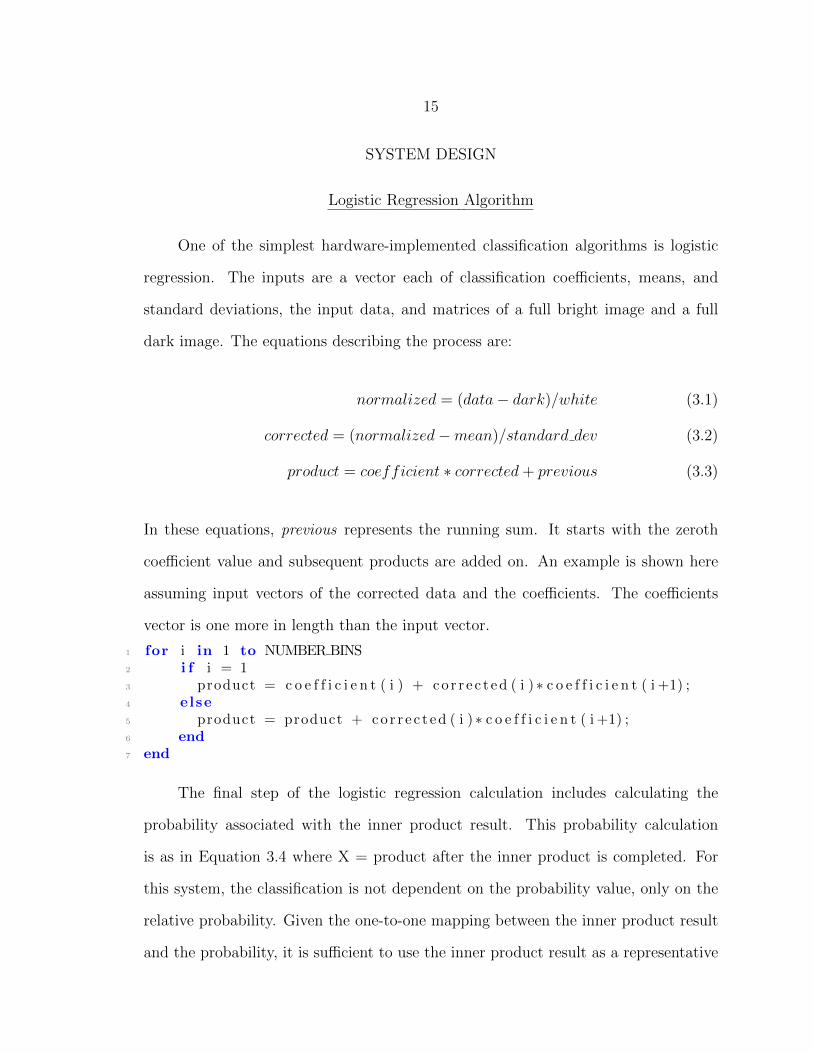
Logistic Regression Algorithm
One of the simplest hardware-implemented classification algorithms is logistic
regression. The inputs are a vector each of classification coefficients, means, and
standard deviations, the input data, and matrices of a full bright image and a full
dark image. The equations describing the process are:
normalized = (data− dark)/white (3.1)
corrected = (normalized−mean)/standard dev (3.2)
product = coefficient ∗ corrected+ previous (3.3)
In these equations, previous represents the running sum. It starts with the zeroth
coefficient value and subsequent products are added on. An example is shown here
assuming input vectors of the corrected data and the coefficients. The coefficients
vector is one more in length than the input vector.
1 for i in 1 to NUMBER BINS2 i f i = 13 product = c o e f f i c i e n t ( i ) + co r r e c t ed ( i ) ∗ c o e f f i c i e n t ( i +1) ;4 else5 product = product + co r r e c t ed ( i ) ∗ c o e f f i c i e n t ( i +1) ;6 end7 end
The final step of the logistic regression calculation includes calculating the
probability associated with the inner product result. This probability calculation
is as in Equation 3.4 where X = product after the inner product is completed. For
this system, the classification is not dependent on the probability value, only on the
relative probability. Given the one-to-one mapping between the inner product result
and the probability, it is sufficient to use the inner product result as a representative

16
of the relative probability for each class to determine the class that each pixel most
likely belongs to.
P =1
1− e−X(3.4)
To ensure that the computations are hardware-friendly, only multiplications and
additions are implemented. This means, that any numbers needing to be divided are
first inverted in the software before being ported to the hardware. The computation
of logistic regression involves matrix inner products. Given normalized inputs and
classification coefficients, the inputs are multiplied by the corresponding coefficients
and a running sum is kept over a pixel to achieve a single result representing the
probability that the pixel belongs to that class.
Figure 3.1: Inner product calculation with vector of coefficients and matrix ofnormalized values with dimensions of number of bins by number of pixels.
The normalization that takes place uses the white and dark values that are
passed with each data input as well as stored mean and standard deviation values that
represent the mean and standard deviation across the spectral bins from a training
set. The white and dark values are used to normally distribute the data between 0
and 1, while the mean and standard deviation account for the frequency of particular
values. The dark value is subtracted from the data and the result is multiplied by
the inverse white value. Subsequent operations involve subtraction of the mean and
multiplication by the inverted standard deviation. The inverse of both the white
values and the standard deviations are calculated externally before being stored in

17
system memory so no hardware divides are required, enabling fewer resources used
and faster clocks.
Hardware Elements
Arria 10 SoC
The Arria 10 SoC by Altera (which was acquired by Intel in 2015) was chosen
for the primary computation engine on this project for several reasons. The primary
reason is its hardened floating point units which enables the device to allow for over
1.5 trillion floating point operations per second of performance [12]. This is the
first device on the market to contain single-precision floating-point multipliers and
adders incorporated into the hard DSP blocks [12], the addition of which provides
a great improvement in system development since fixed-point algorithms take much
more effort to develop and soft floating-point calculations use unnecessary amounts
of resources to create floating-point multipliers in the FPGA fabric. In addition,
the largest device in this family has 660K logic elements (LE), over 42Mb M20K
memory, and up to 48 transceivers capable of 17.4 Gbps [11]. This device is the
best middle-class FPGA on the market today. Future iterations of this system could
utilize different versions of the Arria 10 or move to a higher-end device in the Stratix
10 (the largest of which will have around 30 billion transistors [13]). The Arria 10
is the best FPGA for this purpose right now because of its high performance, which
surpasses the speed requirements of the cameras, for data alignment purposes while
still maintaining affordability. Also, the Stratix devices, while better in number of
logic elements and DSP performance, really excel in transceiver performance and
are best suited for tasks involving high transmission. Though this design does use
transceivers, and may benefit in the future from moving to these more advanced
18
devices, it is not necessary to have the higher capability given the limit of the data
rate from the cameras.
Development Board Components
In addition to the Arria 10, other components on the development board that
were utilized for this project include the DDR3 DRAM, the SMA connectors, and
the FMC connector. The DRAM on the board is 1 GB of memory for each of the
FPGA and HPS to utilize. This is used for storing the light and dark matrix values.
The SMA connectors are used as the interface for the transceivers to communicate
with the Arria V FPGA. A daughter card was developed to plug into the FMC for
the purposes of bringing camera data into the FPGA.
Also an important part of the project is the Arria V SoC, which is also on
a development board that includes SMA connectors, an FMC connector, a Max V
CPLD, and a programmable oscillator. The SMA connectors here are again the
interface for the transceivers. The FMC is used for the custom daughter card to
connect the monochrome camera to the FPGA and the oscillator is utilized for
achieving the ideal clock frequency for the transceiver communications. The oscillator
is programmed over I2C by the Max V, which has to be programmed separately
prior to running the desired program on the FPGA. The high level diagram of system
components is shown in Figure 3.2. Not shown is the external PC which will interact
with the HPS over Ethernet. While in future system implementations, the Arria V
will be replaced with an Arria 10, it is currently used for the monochrome camera
subsystem because of its initial use in the development of this subsystem.
Additional Custom Boards
In addition to the two FPGA development boards the project also required the
creation of several daughter cards, i.e. printed circuit boards (PCBs). Three cards

19
Figure 3.2: High level view of the components external to the SoC utilized in thesystem. The colored regions depict the individual PCBs.
were developed using the PADS software from Mentor Graphics [14], by teammates
Connor Dack and Alex Matejunas. The first card is designated the ’sensor board’,
which contains all of the circuitry to connect to the lines of the CMOS sensor chosen
to be the face for the hyperspectral front-end. All of the lines are drawn out to two
100-pin ribbon cable connectors. This board is separate for the purposes of being
able to orient at a 90◦ angle to the rest of the boards, but also so it is modular and
could be easily swapped with a different sensor, should the need or desire arise. A
second board contains more ribbon cable connectors and connects the data from the
cables to the FMC, which will bring it into the FPGA for processing. This board
also contains circuitry for the transceivers, including SMA connectors and a clock
generator to provide a reference clock, since the Arria 10 development board does not
contain any SMA connectors for transceivers. Both boards are shown in Figure 3.3
connected to the Arria 10 pre-production development board.

20
Figure 3.3: The PCBs created for the hyperspectral camera connection to the Arria10 FPGA. They are shown attached to the FMC, without the ribbon cables andcoaxial cables.
A board was also created to connect to the FMC on the Arria V with inputs
for the monochrome line scan camera’s Camera Link cables. A custom board was
created for this purpose because not all of the FMC pins are connected on the Arria
V development board, though they are needed for communication with the camera.
Consequently, a daughter card was developed to appropriately map the camera signals
to connected FMC pins on the FPGA.
Project Overview
In order to implement a processing system on the FPGA, the tasks required
were broken into system blocks as detailed in the following sections. These blocks are
the camera interface, the DRAM interface, the computation block, and the FPGA-
to-FPGA interface, which encompasses the communication system between the two
boards in order to send signals to the air jet system and transmit object information.

21
Figure 3.4: Block diagram of the full system functionality
Camera Interface
In order to integrate the camera sensor on this prototype system, two additional
boards were fabricated. The first board houses the sensor and has connectors for
the data to pass to the second board, which is connected to the development board
housing the FPGA, and routes all the data signals to the appropriate places to be
accessed from the FPGA as well as ensuring the control signals are appropriately
routed. This board also contains clock generator circuitry and SMA connectors
for transceiver communication purposes. As previously mentioned, the two boards
are connected via ribbon cable in the prototype to allow the sensor to be at a 90◦
angle from the other boards. Configuring the sensor on its own board makes this a
modular product, in which other sensors (on their respective boards) could be used
to replace the current one so long as the signals are routed in the same way through
the connectors.

22
Figure 3.5: Block diagram of the camera interface subsystem.
The programmable hardware interface for the camera consists of a state machine
to compile all the bits per pixel as they are presented, and attaching location
information which describes which pixel and spectral band the data belongs to. It
also pulls the data from DRAM through a FIFO interface and verifies the location
information matches that of the pixel that is being compiled. This interface also
sends any control signals to the camera required for triggering a start and providing
a clock signal to the camera.
The latency in the Camera Interface is determined based on the camera data
rate as well as the number of cycles needed to delay the data before it is passed on
in order for it to be parallelized. Since the data is presented in 10 taps, one bit at a
time, there is a delay needed to accumulate all the relevant bits per pixel per band.
Additionally, to create 5 parallel channels, the data is delayed because it is initially
presented serially. It was chosen to add this delay and parallelize because while it
slows down the initial presentation of the data to the computation unit, the increase
in computations completed through parallel channels is great enough to overcome
this initial serial latency.

23
DRAM Interface
In order to account for the effects of the camera, all incoming data is normalized
by the white and dark values as in Equation 3.1. These are meant to correspond to
the largest and smallest possible data values that have been, or could be, seen. This
data is captured in still images taken prior to operation of the system. The dark
image is taken while the lens cap is on the camera to provide a theoretical darkest
environment possible. In contrast, the light image is captured while the camera is
fixed on a white strip that is lit up to its brightest value seen given the operational
lighting conditions. Given that these are full matrices, with potentially variant values
at each pixel/band, all the information captured needs to be stored. Due to its size, it
was decided to store this data in off-chip Dynamic Random Access Memory (DRAM)
so that there is still plenty of room for more frequently accessed and changing data
in the on-chip SRAM memory. This was also deemed an acceptable choice of storage
location because the values are only accessed before the computations and on-chip
memory is used to buffer the values as they are accessed, so there is less time-critical
need of the data from the time of address specification (i.e. the DRAM matrix values
are pre-fetched, alleviating any effects of DRAM refresh stalls).
DRAM consists of a grid of capacitors and transistors where each capacitor is
capable of storing a single bit based on its voltage level. The transistor is used to
access that particular capacitor and charge or drain it as necessary. The memory has
to be refreshed occasionally to keep the stored values as the capacitors drain their
charge over time. Since each stored bit only requires a single transistor and capacitor,
this memory is very dense and cheap, making it attractive in industrial applications.
However, DRAM is not quick to access in comparison to SRAM that is located in
the FPGA fabric. The timing of controller interactions with the memory is also
24
Figure 3.6: Block diagram of the memory subsystem.
very technically challenging, but is handled through a hardened memory controller in
the FPGA that provides the direct interface functionality. A custom controller was
developed to be the master of this interface and this controller issues read or write
commands.
As camera data enters the system, prior to being processed in the computation
subsystem, it needs to be properly aligned with the corresponding location’s white
and dark matrix values. In order to accomplish this, the matrix values are pulled
from memory sequentially in the same order that camera data is received. It is stored
in such a way that this order can be accessed sequentially in the memory. By doing
so, bursting access, reading multiple address locations in multiple sequential memory
accesses, can be used to take advantage of the structure of DRAM. A pre-buffering
system is in place to hold the bursting read data and enable alignment with the data

25
that is coming in faster than the DRAM can be accessed, if each location were to be
read individually. The white and dark values for each location are stored together,
requiring only one memory access per location. This was done to facilitate ease of
access and use as both values need to be aligned with the incoming data. Additionally,
the bus between DRAM and the FPGA can sustain signals of the width needed to
accommodate each of the data values and the location (see Table 3.1). This buffer’s
output is made available to the camera interface to enable the data alignment with
incoming values.
Table 3.1: Information Associated With a Pixel in DRAM
127 031 ZERO PADDING 0 31 LOCATION 0 31 DARK 0 31 WHITE 0
Computation Unit
The pixel and object classifications are done in the computation unit. This block
consists of the normalization step as well as the inner product engine to complete the
classification. It also compiles a full object classification, sorts the results, and makes
a decision at the end. The system is using linear regression to classify the pixels,
as was introduced in Section 3, Logistic Regression Algorithm. Presented below is a
detailed explanation of the block to classify the pixels, then subsequently the objects.
Pixel Classification In order to perform the logistic regression calculation on the
incoming pixels, there are a number of parallel blocks implemented. The first is the
normalization which performs the calculations in Equations 3.1 and 3.2 on the incom-
ing data in parallel. At this step there is a DSP block per calculation step per parallel
data channel. The mean and standard deviation values are stored in on-chip RAM for
easy access. The output of the normalization is passed to the inner product blocks.

26
Figure 3.7: Block diagram of the computation subsystem.
There is an inner product block for each class within each parallel channel. This
corresponds to NUMBER OF CLASSES*NUMBER OF PARALLEL CHANNELS
DSP blocks, as each inner product requires only one DSP unit. For this prototype
design, that means there are 16 ∗ 5 = 80 parallel DSP blocks used for the inner
product. The class coefficients are located in memory blocks for each class, addressed
by band number. At the end of each pixel, the results of the inner product blocks for
each parallel channel are added together to have one result per class. The output,
then, is a vector of probabilities designating how likely it is that the pixel belongs to
each class. This information is stored in on-chip memory for access by the user, as
well as being passed to the object classification subsystem.
The computational complexity of this classification is found by analyzing the
number of operations that could be happening at any one time. Once the system is
fully in operation, all of the normalize DSP blocks and inner product blocks can be
running at once. Assuming this is the case, the performance of the pixel classification
when running on the 70 MHz data clock with a 210 MHz operation clock is 4.55
GFLOPS. Concurrently, the on-chip memory bandwidth can be analyzed for each
of the instantiated memory blocks. Taking in to consideration the blocks for the

27
means, standard deviations, classes, intercepts, and results, the total on-chip memory
bandwidth is 44.8 GBytes/s. Much of the data pulled from these memory blocks is
actually not used, but is required to fulfill acceptable memory port width ratios. This
number was found using the 70 MHz clock rate that is used to read or write to the
memory on the processing side of the system.
Object Classification In classifying the full object, data is utilized from the
monochrome line scan camera as well as the pixel classifications obtained using
the hyperspectral data. The line scan camera is taking images at 80,000 frames
(lines) per second (fps) and the Arria V FPGA is performing calculations to find the
location of an object. The line scan line number and pixel number are translated into
the corresponding hyperspectral numbers on the Arria V to prevent transmission
of numerous repetitive entries. This translation is done because the monochrome
pixels are at a much finer resolution than the hyperspectral pixels. Information
about the object’s location is transmitted to the computation block including the
line number, an object number, and the beginning and ending pixel in that line that
defines the object. A record is kept in the computation unit on the Arria 10 of object
locations, which is used to accumulate pixel classifications within each object. After
an object disappears from the scan line, the overall results are used in a lookup table
to determine if the highest level classification probability is good or bad, though
future systems could look at the accumulated class probabilities of all the classes to
make a decision. The decision to eject the object is made off of this lookup and
sent to the Arria V, which is also controlling the air jets. The final sorted results
are made available to the HPS through a streaming process which feeds a modular
Scatter Gather Direct Memory Access (mSGDMA) block that will write streaming
data to SRAM belonging to the HPS.

28
Since not every pixel will need to be accumulated into an object, and pixel
results do not show up every clock edge, there is only one DSP block implemented in
this section. If it were constantly in operation, it would achieve a performance of 70
MFLOPS. The memory block that holds the accumulated results for each object has
a theoretical maximum bandwidth of 4.48 GBytes/s. This is theoretical because, as
with the adder, there will not be a memory access on every clock period due to the
intermittent nature of the data that will be accumulated.
The VHDL code for operation of the computation subsystem can be found in
Appendix B. These files are
• computation unit.vhd
– regression.vhd
∗ normalize.vhd
∗ channel sum.vhd
– sort.vhd
– object tracking.vhd
FPGA Interface
In order to communicate between the two camera subsystems, a high-speed (6
Gbps) serial interface was designed to connect the Arria V and Arria 10 FPGAs. The
monochrome line scan camera is connected to, and its data is processed on, the Arria
V while the hyperspectral camera is connected to the Arria 10 where the inner product
computations for classification occur. In order to make a full object classification, the
information about each object’s location needs to be passed from the Arria V to the
Arria 10 and the ultimate decision to keep or discard each object is sent back from
the Arria 10 to the Arria V, which also controls the air jet system. One reason for

29
Figure 3.8: The connection between the Arria V development board (top) and theArria 10 development board (bottom).
the two separate boards is the availability of FPGA Mezzanine Connectors (FMC)
on the development boards. The monochrome line scan camera requires two Camera
Link cables between the Arria V and the camera. The FMCs are connected to the
FPGA in such a way that both connectors are required to connect all the desired
signals for the camera. There are only two FMCs on the Arria V development board,
and consequently, both are used for this camera. The hyperspectral camera also uses
an FMC to connect to the FPGA. Since the Arria 10 is the larger device and includes
hardened floating point, it is imperative that this board is used for connecting to the
30
hyperspectral camera. Since a daughter card has been developed such that all the
correct signals are routed to one FMC for the monochrome camera, both cameras
could be connected to the Arria V but not the Arria 10 as the available board only
has one FMC. The Arria 10 board currently contains an engineering sample (pre-
production) version of the Arria 10 since we have not been able to get a production
evaluation board of the Arria 10. The production evaluation board will have two
FMCs and at that time, the full design can be ported to one board, provided the
logic will fit on the device, eliminating the need for the communication interface.
Unknown at this point is if the Arria 10 has enough resources to fit the full design or
if two Arria 10 FPGAs will be needed.
The communication interface between the two FPGA boards is through SMA
connectors connected to coax cables that use the high-speed transceivers in each of
the FPGAs. Using the SerialLite2 protocol, the transceivers can establish a link and
transmit data. SerialLite is a communication protocol that is particularly good for
high-speed serial communication and has less overhead than other serial protocols.
The protocol includes CRC checking as well as optional scrambling/descrambling
of the data. It can also be used with multiple receivers and a broadcast mode,
if desired. Though the SerialLite2 IP core provided by Altera is not yet readily
available for the Arria 10, it is indirectly supported. Since SerialLite3, which is
available for the Arria 10, is not compatible with SerialLite2 due to different encoding
schemes and packet structure differences, the SerialLite2 core was needed to be able
to communicate between the two boards. In addition to the SerialLite2 core, the
native transceiver phy cores are used for their respective devices. These implement
the PMA (physical medium attachment) aspect of the transceivers as well as some of
the PCS (physical coding sublayer) and handle the physical transmission of the data.

31
The SerialLite2 core then sits on top of the native core and handles additional PCS
tasks of transmission, such as providing a CRC for the data.
In order to set up the reference clock, which is required to be 156.25 MHz to be
compatible with the general transceiver accepted reference clocks, a programmable
clock was needed. At first, this was done using the programmable oscillator on the
Arria V development board, which provides the reference clock to the transceivers
that are connected to the SMA connectors on the board, and is programmable over
I2C from the Max V CPLD controller. After the FMC breakout board was completed,
in order to provide additional SMA connectors for testing of the transceiver channel,
the clock generator on the breakout board had to be programmed over I2C from the
FPGA to generate the desired frequency clock. The clock generator chosen for this
purpose has four one-time programmable (OTP) configurations, so that the correct
frequency can be loaded on power-up. After programming the volatile RAM with
the desired values, they were burned into a configuration on the OTP memory of the
generator and subsequent projects need only enable the output of the clock generator
to get the desired frequency. This made it much easier to ensure the right frequency
was available at transmission time, rather than programming the clock each time the
power was cycled.
On the Arria 10 pre-production development board, the FMC breakout board
can be used, however the reference clocks connected to the clock generator outputs
do not connect to the reference clock inputs on the same bank as the populated
transceivers. One of the reference clocks on this bank is provided by a programmable
oscillator on the development board that has approximately 10 clock outputs. Instead
of programming yet another oscillator, the SMA clock outputs were found to provide
a 156.25 MHz clock that can be transmitted over SMA to one of the receivers to be
used as a reference clock on the breakout board.
32
Performance
A significant benefit of this system is the increase in performance from the
previous method of processing. Previously, Resonon has been using a camera with a
frame rate of 140 fps with a spatial resolution of 640 pixels and a spectral resolution
of 240 bands. This system under development is comprised of a 500 fps camera sensor
(full resolution) running at 2000 fps (partial resolution) with a spatial resolution of
1024 pixels (reduced to 256) and a spectral resolution of 160 bands. A large increase
in spectral bands was neither needed nor desired by Resonon because they have found
that the data becomes redundant and unuseful after a certain point. With a clock
speed of 70 MHz on the computation side and approximately 157 cycles to classify
a pixel, this means that it takes only 1.57µs to compute the classification for a full
pixel. With 1024 pixels, this hyperspectral computation takes 1.6ms per frame (i.e.
line scan).
The monochrome line scan camera can run up to 80,000 lines per second,
and the transmission rate between the two boards is at 6250 Mbps. With 54 bits
needed to represent the information per object per line, objects are transmitted
at a rate of 115.74 MHz. When packaged in 32-bit data words and including
start and end packets, the transmission is still accomplished in 20.48ns. Since the
monochrome line scan calculations can run on an 83.5 MHz clock, it is able to keep the
transmission buffer full (i.e. calculations take place faster than they are needed), but
not overflowing since there will not be objects found on every clock edge. The decision
on the hyperspectral side is made using the 70 MHz clock that the computation unit
runs on, so there may be some dead spots in the return transmission. Upon receipt of
the object information, the line and pixel numbers are stored using the object number
in an array updated with each transmission to note where objects are on the line.

33
IMPLEMENTATION DETAILS
Programmable Oscillator
In order to achieve an accepted clock frequency for the transceiver reference clock
on the Arria V board, a clock generator had to be programmed. The first iteration
involved programming the programmable oscillator, a Si570 device from Silicon Labs,
provided on the development board. In order to achieve the desired frequency of
156.25 MHz, 6 of the available registers are required to be programmed via the I2C
lines which are connected to the MAX V CPLD system controller that is also on the
board. The oscillator does not have persistent memory, so it must be reprogrammed
after every power loss to consistently have the desired frequency on every run of the
device. This can be arranged by programming the Max V to run the I2C code as
part of the device configuration. Programming the oscillator requires knowledge of
the current frequency and register values as the calculations for new values are based
off the current configuration. These default values and the new values were obtained
using the Clock Controller GUI provided as part of the board test system from Altera.
Registers
The device has two sets of identical registers, one set for devices with 20 or
50 ppm temperature stability, and the other for devices with 7 ppm temperature
stability. The oscillator provided has 7 ppm temperature stability, 20 ppm total
stability as determined by the part number. The critical values needed to program the
registers are the output divider values (N1 and HS DIV ) and the crystal frequency
multiplication ratio (RFREQ). The output dividers are found by changing the
existing values as little as possible, but keeping the digitally controlled oscillator
(DCO) frequency within the acceptable range of operation. The factory default is

34
a 100 MHz clock with divider values and DCO frequency as shown in Figure 4.1.
Using the GUI, the necessary values to program were easily obtained as shown in
Figure 4.2. Though provided by this tool, they could also be found using a couple
of equations, which were utilized in the MATLAB script created to print the VHDL
constants for the programming of the registers. Based on the required values, all the
registers needed to be programmed with values as shown in Table 4.1. The steps to
derive these values are in Equations 4.1, 4.2, and 4.3 [15].
The RFREQ value is a 38-bit number with 28 decimal places, so is divided
by 228 to achieve the correct decimal value prior to performing the calculations and
multiplied by 228 at the end in order to shift the decimal accordingly. The values
for HS DIV and N1 are chosen from a selection of allowed values with the goal of
minimizing the DCO frequency (fdco) within an acceptable range, and also achieving
the lowest possible N1 and the highest HS DIV .
fxtal = (f0 ∗HS DIV ∗N1)/RFREQ (4.1)
fdco = f1 ∗HS DIV ∗N1 (4.2)
RFREQ = (fdco/fxtal) ∗ 228 (4.3)
Table 4.1: Register settings for Si570
Register Number Old Value (Hex) New Value (Hex)13 22 A014 42 C315 BC 1316 30 B717 EE 0C18 FA D9

35
Figure 4.1: Factory Default Clock Register Settings for Si570
Figure 4.2: Preferred Clock Register Settings for Si570
In order to perform the programming of the device, an I2C master component
was utilized, provided by Scott Larson on EE Wiki [16]. A state machine was
devised to progress through each of the registers and start individual transactions
with the master driver. Following each write, a stop is sent, rather than continuously
writing in order to ensure that the correct register is written to each time. Since
all registers are written sequentially, this is not a strictly necessary course of action
and all registers could have been written in a streaming write sequence, but using

36
individual transactions ensures that a specific register receives the data designated
for it. This also set up the state machine in a useful manner for the clock generator,
which does not require programming of all registers. The code for the implemented
driver can be found in Appendix B under i2c driver.vhd.
Programmable Clock Generator
In order to further test the transceiver communication, two sets of transceivers
were required. Since the development board for the Arria V only contains one
set of SMA connectors and the Arria 10 engineering sample development board
does not contain any, a daughter card was fabricated to utilize the transceivers
through the FMC connector, with SMA connections. In order to achieve a viable
reference clock on the transceivers utilized by the daughter card, a clock generator
was included on the card along with the necessary circuitry. The VersaClock 6 Low
Power Programmable Clock Generator from Integrated Device Technology was chosen
because it is programmable over I2C, it has two configurable clock outputs, and it
has the option for four one-time programmable configurations stored in non-volatile
memory. The one-time programmable configurations are appealing in this project
because it does not require any setup once the configuration has been programmed;
the required frequency will be available on power-up of the device, unlike with the
oscillator on the development board.
Design Decisions
Many of the additional circuitry required by the clock generator is specified in the
datasheet, with recommendations such as using a 25 MHz crystal, and terminations
for different output configurations [17]. One of the design decision made includes
the connections of the I2C lines and the select line, pins 8, 9, and 24 respectively as

37
shown in Figure 4.3. Pin 24, OUT0 SEL I2CB is used to determine whether pins 8
and 9 will be select lines for one of the four stored configurations or the clock and
data lines for I2C communication. If connected to a pull-up resistor, they will be
select lines, otherwise, they will be used for I2C. Consequently, a pad was placed on
the PCB to enable a pull-up to be used, but it was not populated so the device could
be programmed over I2C. After power-up, this pin also serves as a clock output,
acting as a buffer for the selected reference clock [17]. Each of the clock outputs is
connected to a reference clock pin for the transceivers through the FMC connector
and one of them is also connected to the global clock network for use in FPGA logic,
if desired.
Figure 4.3: Diagram of Pin Assignments for VersaClock 6 Programmable ClockGenerator [17]

38
Registers
The VersaClock Clock Generator has registers programmable for four output
clocks, despite the fact that there are only two output clocks available on the device,
in addition to the reference clock output. The registers available to be programmed
include settings for the internal PLL divider and output dividers, both integer and
fractional. There is also the option to choose between the crystal reference and a
reference clock provided by the FPGA. The pins are shown in Figure 4.3. The registers
chosen to program include those for the programmable capacitors, the internal PLL
frequency dividers, and the output dividers. The values for the programmable tuning
capacitors were chosen based on Equation 4.4 [17] with an estimated combined stray
and external capacitance of 2 pF. Several values were tested to verify the values, but
there was not a large noticeable difference between any of the results, as seen on an
oscilloscope, so the originally designated values were kept. In choosing the values for
the PLL frequency dividers and the output frequency dividers, a voltage controlled
oscillator (VCO) frequency of 1250 MHz was targeted, which is the lower bound
of the desired range for the oscillator. Using this value with the known expected
output frequency of 156.25 MHz meant there was no fractional divider values for the
PLL or the output, which means fewer registers to program in addition to a more
accurate clock division. A MATLAB script was used to print out the desired register
configurations and the resulting VHDL code is included in Appendix A.
CL = (9pF + 0.5pF ∗XTAL[5 : 0] + Cs+ Ce)/2, (4.4)
Burning a Configuration
Unlike with the programmable oscillator on the development board, the clock
generator has the ability to hold four non-volatile configurations. The benefit of

39
using a non-volatile configuration, is that the clock output is available very soon after
power-up, without having to re-program the generator each time. In order to burn a
configuration, all the registers in RAM were set to the desired values, the VCO was
calibrated, and then the registers designated for control of the OTP were programmed
to define the registers to burn and then check to be sure that the burn completed
successfully. By setting bit 7 in the OTP Control register, the part will automatically
load data from OTP on power-up.
Utilizing the Clock Generator
With the configuration needed burned into the part and automatically loaded
on power-up, the only thing needed to ensure that the clock can be used by the
transceivers is to enable the output and select the appropriate reference clock. For
the default configuration burned, the default reference is the crystal input at 25 MHz.
The enable and select signals are both driven low on pins 6 and 7.
Altera IP
Within the Quartus software, Altera provides many different IP blocks as
”Megafunctions” that can be customized and dropped in a design. These make
handling transmission interfaces or creating memory blocks much simpler. However,
in our efforts to make the system as modular as possible, some of these had to be
bypassed and implemented by hand. Fortunately, the compiler will synthesize the
components and create the desired blocks even when not created in a megafunction.
One of the things that require care when writing the block by hand, however, is the
rules of the block. For instance, a dual port memory is very tricky to implement by
hand, as it cannot have arbitrary values on either side of the block. A benefit of
creating the unit within the Megawizard, is the tools will inform the user of valid
40
values for each of the parameters. Without this interface, users must carefully choose
their values or learn of a fail when the design is compiled. This was encountered in
the memory block instantiations used within the computation subsystem.
In order to avoid creating multiple different memory components and also in
an effort to create a modular design, a memory block component was created that
instantiates the Altera altsyncram megafunction with generic parameters that can be
input at the time of instantiation. This is a perfectly reasonable approach until a
port width ratio is violated. Rule violations happened several times over the course
of development and fixing them resulted in the creation of extra locations within the
memory block that were skipped on one port and ignored on the other, but required
to be there to enable the port ratios to work within the block. This is an unfortunate
waste of memory but not a huge concern for the design as it stands currently.
Timing Constraints
The hyperspectral camera is able to produce data at 6.6 Gbps with 500 fps when
using the full 1280x1024 pixel image. Having reduced the image size to 256 pixels for
this application, the frame rate is up to 2014 fps. After compilation of the parallel
data streams, it will be passed into the computation unit at 66 MHz. In order to
stay ahead of the incoming data, the computation unit needs a base clock at least
this fast, though preferably faster. Fortunately, faster is possible. The base clock in
the regression unit is targeted at 70 MHz. One of the tricks in running faster than
data is produced is to ensure that the blank times are not affecting the overall results,
since the unit is constantly adding in new values over each pixel. Therefore, a signal
was added to classify each incoming data chunk as valid or not. Using this signal,
the computation unit determines whether or not the value should be added into the
existing calculations. The valid signal is not, however, the antithesis to the error

41
signal passed by the camera block. Error is set when the incoming data is bad or the
location of the white/dark matrix values does not line up with the location of the
incoming data. In this case, the pixel currently being calculated is zeroed out and no
incoming data is considered until the start of the next pixel.
The design uses two primary clocks for the computations and classification, one
with a frequency three times faster than the other. The slower is required to keep up
with the incoming data rate. The triple speed clock was included when it was found
that the floating point adder and multiplier each take three cycles to complete. In the
original design of the inner product unit, a multiplier was pipelined with an adder, but
the result from the adder was needed as an input to the multiplier for the following
calculation. This was a carryover from a previous implementation which received data
from each spectral bin at a time, rather than from each pixel. Once the design was
changed to accommodate data arriving for a full pixel before moving on, the inner
product unit could also be changed. Quartus provides a multiply-accumulate floating
point megafunction that completes in four cycles. Using this, the faster clock was no
longer needed in this unit and data alignment was much easier. The faster clock was
kept, though, and utilized in the normalization step and combination of the parallel
data for the benefit of speed.
A challenge encountered in the timing requirements of the computation unit was
achieving the correct setup and hold timing for each of the clocks and a maximum
frequency of the clocks that is at least the desired run frequency. The Quartus
software contains a timing analyzer known as TimeQuest, which will check paths and
analyze timing requirements as well as providing statistics on each of the paths. It
will also provide some recommendations to help close timing, when possible. With
the first inner product unit design, TimeQuest found the faster clock with a maximum
rated frequency of 100 MHz less than where it needed to be in order to be triple the

42
speed of the other clock. This issue was the primary motivation for changing the
design of the inner product unit. The paths that were failing setup timing were all
related to the inner product and the Chip Planner, another tool within Quartus, was
used to show the paths that were being taken. In most cases, the path involved an
unnecessary stop at a register before passing back into the DSP block. By switching
out the adder and multiplier for the multiply-accumulate megafunction, there was a
significant decrease in required paths and registers. Therefore, routing was simpler
and clocks were not bouncing around nearly as much with fewer registers required.
There were a few changes made in order to accommodate the new architecture, but
it helped with timing immensely and functionality was verified in MATLAB. The
change allowed for the faster clock to have a maximum frequency up to 100 MHz
faster than its required speed and the slower clock also has a significant increase in
the ceiling for its speed. The setup timing failures were also removed with the removal
of the extra registers outside of the DSP blocks.
In analyzing the compilation results generated by Quartus, it was found that the
software was optimizing out several design-critical signals, including the data inputs
which caused much of the subsequent logic to also be optimized out. After issuing
a few changes to combat these optimizations, including fixing the parenthesization
around signal indices and utilizing the ’noprune’ attribute, new timing errors were
uncovered. This is one of the biggest tricks in working with software programs and
large projects. There are limitations to sizes of the inputs, and the optimizer will
remove seemingly unused signals. If the developer is unaware of these optimizations,
they could be placed in a false sense of security. Fortunately, this was discovered and
the work done to check if the removals were legitimate. Most of them actually were
because of extra space allocated in a signal that ends up never changing or remaining
unused.

43
The timing battle continues when the full design is compiled together. Not only
is the routing more challenging, new setup timing errors are uncovered because of
the routes taken. Though floorplanning was attempted, in most cases it actually
prevented the fitter from being able to fit the design. This simply continued the need
for timing analysis and tweaks to re-achieve minimal setup and hold errors in each of
the clocks.
Toolchain Fights
Some of the greatest frustration in implementation of the design, was simply in
figuring out how to work with and achieve the desired results from the tools utilized.
Oftentimes, it was a matter of tweaking settings in the software to display what you
want to see (and that is actually occurring), rather than a problem with the hardware
code that is being tested.
SignalTap
Altera provides an internal logic analyzer to watch signals in a design that could
not be reached from an external analyzer. This is helpful in debugging a design,
however since the logic analyzer uses device resources in the FPGA, anytime a change
is made in the analyzer, the design has to be re-compiled. Additionally, the extra
resource usage could make it a challenge for large designs. In this case, it is best for
modular designs when you can break out a portion to look at without requiring the
full design. This was a frequent problem encountered when debugging the part of the
project that communicates with the external DRAM because there was no other way
to look at the signals, and the particular signals that this project is passing in and
out of DRAM are 128 bits wide, so they each take up a lot of resources. The trick,
44
then, is to choose only the signals critically needed to be looked at and minimize the
size of the overall project to be scaled up after debugging is completed.
TimeQuest Timing Analyzer
Altera’s Timequest Timing Analyzer is both a useful tool and a nuisance. It is
helpful in predicting timing and showing what the maximum achievable frequency is.
However, it requires proper user input to help interpret how data is moving through
the design and how different clocks are related. Given the use of a clock that was
set to be three times faster than another clock and data that moved freely from one
clock’s domain to the other, interpretation for the tool was critical. Without it, the
setup and hold analysis had a total failure through the system of hundreds of seconds.
The needed input was the correct multicycle paths to tell the tool how to analyze
data that crosses clock domains between the system clock and the triple-speed clock.
By adding this information, the setup time error went from hundreds of seconds to
twenty seconds for the whole project. Further, upon changing the inner product unit,
the maximum frequency of the clocks was correctly above where they need to be and
the setup time error was completely mitigated. However, upon removal of some of the
optimizations that were compiling away needed registers, some of the setup timing
errors returned. These occurred mostly in the line scan camera side of the project,
as the object is ’built’. It is anticipated that utilizing the clock from the transceiver
block that actually corresponds to the line scan data will fix some of those errors.
Chip Planner
The Chip Planner utility provided with Quartus is extremely useful in visualizing
where resources are being used and the proximity of certain resources to each other.
It displays where each of the registers, DSP blocks, and I/O are being used for the
design after a compilation. It will also show data paths and can be linked to from
45
TimeQuest for viewing critical paths. A useful aspect that helps with timing is the
floorplanning feature. As the designer for the project, I was able to group signals
together and instruct the fitter to place them co-located. In doing so, the compile
time was decreased because paths were found easier and the clock speed increased.
This is not always the case, though. When a floorplanning technique from a project
containing only the regression step was applied to the project containing the full
computation unit, the fitter was unable to fit the design. This is likely due to the
significant increase in size of the overall project, so the additional resources and paths
prevented the use of the same techniques for fitting as were utilized in the smaller
project. Nevertheless, even grouping a small portion of the design together assisted
the fitter in finding placement for the whole design sooner and in a more efficient
manner than if it were to do it itself without clues as to the grouping. Grouping
for floorplans was particularly helpful in this project because of the way the design
is implemented. Due to the many generate statements used for working with the
parallel channels, it is helpful to the fitter to define what data is moving through each
path since as the user, that should be clear. In doing so, the fitter is able to try and
place the appropriate signals and data paths in proximity to related paths. A fitted
floor plan for the production Arria 10 development board is shown in Figure 4.4.
MATLAB
The design was verified using the HDL Verifier toolbox available within the
MATLAB tool set. In order to use this with the floating point computational blocks,
there are a few specific files that need to be included in a particular order to ensure
correct compilation with all libraries able to be located. Using this method, in
conjunction with ModelSim cosimulation, was useful in verifying the design, but not
easy to figure out at first. The HDL verifier is particularly useful in large projects

46
Figure 4.4: A fitted floor plan in the Arria 10.
such as this because it will provide inputs to the system and the outputs can be
compared with MATLAB calculations for easy verification. However, it was also
useful to have Modelsim running the design because it was sometimes easier to follow
the data path through each of the signals visually, rather than trying to pull out
the right information on the outputs. This was also a way to track internal signals
without having to port them out.
Verifying with MATLAB is an exercise in making sure that the functionality
of the design is fully understood. It has to be programmed in both the MATLAB
language as well as the hardware that you are testing. Because it is user code testing
user code, it is important that the desired functionality is fully understood and the
MATLAB code is believed to be correct. It is often necessary and useful to do a
couple of iterations by hand in order to assure oneself of the working nature of the
MATLAB program. When this does not happen, the debugging process is infinitely
more frustrating. This was experienced in testing the regression system. MATLAB
was used to provide the inputs and upon receiving an interrupt, it read the outputs
from the registers and wrote them to a file. The results in this file were compared

47
to those found by MATLAB on the same inputs to determine accuracy. At first, it
appeared to be working. Upon switching the regression to use an accumulator in the
inner product block, verification became somewhat dicey. Though the MATLAB code
did not change, the results from the VHDL could not be made to match it, and the
VHDL made sense. Upon closer inspection, it turned out that the MATLAB script
was calculating the inner product inaccurately and thus, previous results were also
inaccurately verified. The updated MATLAB script was verified by hand for a couple
pixels to assure users that it was indeed correct. With this change, the VHDL was
also verified to be accurate. This blunder provided an important lesson in verification
as it would not have been discovered if the inner product unit had not changed.
MATLAB was also used to generate the code for the register constants that
would be sent over I2C to the clock generator. By modifying a previously existing
script, the register definitions could be documented with the defaults and the desired
values. For any future changes, the user can simply change the values in the script
and re-generate the code. It generates a series of constant definitions to be pasted in
the VHDL file that controls the command transmission. The HDL Verifier was used
to verify functionality of the I2C driving state machine to ensure that the address,
register address, and data are sent and able to be acknowledged correctly.
Toolchain Tricks
As previously mentioned, it was often the case that timing or optimization errors
were the cause of misinterpretation by the tools of the desired design. Many of
the changes made included manipulating settings in the software to provide assisted
interpretation for the Quartus toolchain. These changes are detailed in this section.
In Quartus, attributes are used to assist the tools in interpretation and ensure
that particular conditions are kept in contrast to what might be readily perceived.

48
One of these attributes is ’noprune’. This is used to keep the synthesis analyzer
from removing a signal from the design. It is declared in the architecture prior to
the ’begin’ statement as a boolean. The boolean is then assigned to the appropriate
signal and set to ’true’. This was used in the object tracking file for the purpose of
ensuring that the tracking array was kept completely in the design. See Appendix B
for the object tracking.vhd file and the usage of ’noprune’.
An additional resource to assist in design compilations is the Compiler Settings
found in the Settings menu of Quartus. Within this section, there are Advanced
Settings available for both Synthesis and the Fitter. These settings were used
primarily when the design was having troubles fitting in the device. Some of the
changes made include, in the Fitter settings, changing the optimization technique to
optimize for speed, changing the fitter seed value (a random number, different from
the default, was used), setting the optimization mode to ’high performance effort’,
and setting the fitter aggressive routability optimization to ’always’. Many of these
settings default to ’automatically’ or ’off’ or if a range is possible, the default is the
middle option. Changing these settings alerts the tools to the user’s priorities in the
design and ensures that the maximum possible effort is placed in fitting the design to
the device. The changes made for this design were done to prioritize timing closure
regardless of increases in compile time or increased difficulty in fitting, so long as a
fit was achieved.
Using the Chip Planner to set Logic Lock regions is another useful way to
assist in the fitting of the device and optimizing for timing. Setting these regions
requires knowledge of the signals or resources that should be included in each region.
Incorrectly setting these could cause the fit to fail. Both scenarios were experienced
in the development of the computation system and the full system. However, the

49
regions were used to separate out the parallel resources for ease of interpretation by
the tools.
50
TEST AND VERIFICATION
Camera Interface
The interface responsible for taking the data from the camera, combining it
with data from the DRAM FIFO, and assigning location information was tested via
MATLAB cosimulation and Modelsim. This was done by simulating the data from
the camera with memory blocks per tap and assigning location information - verifying
that the locations were being assigned correctly. Subsequently, the DRAM interface
was added and the steps of writing to the DRAM and pulling from it in addition
to combining location information with the incoming camera data was tested and
verified using SignalTap. A couple of different scenarios were checked, such as if the
location from DRAM does not match the expected location corresponding to the
camera data location and the error flag needs to be set and all subsequent data can
be ignored until location zero is encountered again.
DRAM
The interface with the DRAM was primarily verified using the SignalTap Logic
Analyzer. An incrementing counter was written to the DRAM and then the same
space was read sequentially in a repetitive fashion to ensure that the memory
controller is functioning correctly. This was further verified with the use of the
buffer on the read side when combined with the camera interface. At the time of
this publication, the interaction between the HPS and the DRAM had not yet been
verified, though can be done by passing the values read on the FPGA back to the
HPS for comparison to the values originally written to the memory.

51
Computation Unit
The computation unit was developed and tested in sections. All sections were
verified using MATLAB cosimulation. First, each of the components within the
regression calculation were developed and tested individually. These are the inner
product unit and the normalization block with corresponding test bench scripts
inner product tb.m and normalize tb.m that can be found in Appendix C. The
functionality of the megafunction which converts the fixed point numbers to floating
point was verified with the normalization block. Testing incrementally in this way
was also used to assist in the development of the component as a whole as it relies
on knowledge of the latency through each block to trigger some signals, such as the
signal indicating that a new pixel is beginning in the inner product or a result is
ready on the output. The inner product block was tested with the normalization by
inputting the values from MATLAB on the input ports and using the known latencies
to verify the output before the full unit was tested as it is expected to be used. This
means utilizing the Avalon memory mapped interface to read and write registers and
accessing the results from memory after triggered by an interrupt. This interrupt was
later moved in the full computation unit to be utilized for a different memory block.
The full verification of the regression was completed by writing the class coefficients,
mean and inverted standard deviation values to memory and piping in the input
values after setting the enable bit and interrupt enable bit. Upon completion of the
image matrix, the test bench spins on the interrupt until it is set. At this point, it
reads from the results memory block. The results read from the system are written
to a spreadsheet along with the expected values, as calculated in MATLAB, and
compared for accuracy. After satisfactory completion of this test, a full frame of a

52
small image is tested to verify that accurate results are obtained for each line in an
image. The test bench file for this verification is regression tb.m (see Appendix C).
Other components of the computation unit verified individually in MATLAB
include the sorting block and the object classification block. The sorting block was
verified by reading the print out of sorted results to visually check that they are sorted,
and then checking that the indices line up with the sorted results (see sort tb.m in
Appendix C). The Modelsim output was analyzed to verify the expected two clock
cycle latency for sorting. This verification was also useful in determining the order
in which the elements are sorted, whether from least to greatest or vice versa so
as to correctly interpret the results internally to the computation unit. The object
classification block was verified by creating a few sample objects in Paint that are
simply black on a white background for a clear distinction. The image was read into
MATLAB and the resulting data was used as the simulated transmission from the
monochrome line scan camera. A small section was used to check that the correct
classification results were being compiled over the object and a definitive answer was
correctly given at the end of the object (see objects tb.m in Appendix C). Originally
developed within the object classification block is a component which converts the
monochrome pixel number to the hyperspectral pixel number. This was also verified
individually in MATLAB using camera ratios tb.m (see Appendix C) by generating
a plot to relate the hyperspectral pixel numbers with the monochrome pixel numbers
as shown in Figure 5.1. Figure 5.2 shows a section of the same plot, depicting the
nature of the relations. This component was moved to the Arria V side of the system
to alleviate the need for an excessive number of transmissions.
Due to the nature of having inputs running on several different clocks, testing of
the full computation unit from camera interface input to results of object classification
has not been performed in simulation, but with each of the components working as

53
Figure 5.1: Generated plot depicting ratios between the pixels of the line scan cameraand the pixels of the hyperspectral camera.
Figure 5.2: Generated plot depicting ratios between the pixels of the line scan cameraand the pixels of the hyperspectral camera, zoomed in for greater detail.
expected, the author is confident in the full system functionality. This will be tested
further as development continues.

54
FPGA to FPGA Transmission
The interface using the transceivers was verified by first sending information
between two different transceivers on the same board, before trying to link the two
boards together. The packet generator was sending counter values and the checker
was looking for counter values independently enabling this same system to be used
when transmitting between the two boards. The packet generator and checker systems
were provided in a design example from the Altera Wiki [18]. Signal Tap was used to
check error signals from the pattern checker and the SerialLite2 core. In verifying the
transmission between boards, different transmission speeds were tested, including the
maximum rate that the Arria V can support, 6.5536 Gbps. At this rate, there were
significant errors in the transmission as bits flipped. The goal was to have at least 6
Gbps and this was achieved with minimal errors at a transmission rate of 6250 Mbps,
or 6.250 Gbps. The high-level files relevant for this testing are:
• a10 com.vhd
– xcvr core.vhd
∗ a10 phy.vhd
∗ sl2 core.vhd
∗ xcvr pll.vhd
• packet generate.vhd
• packet verify.vhd
The xcvr core.vhd file can be found in Appendix B, as can the top-level a10 com.vhd
file. The others were either provided by the design example or generated in the
Megawizard for use in the project. A similar structure was used for testing on the

55
Arria V and the top-level file for that project (a5 com.vhd) can also be found in
Appendix B.

56
CONCLUSION
A dynamic and powerful real-time image processing system is being developed
on an FPGA for application in sorting systems. The Arria 10 FPGA is utilized for
its high speed transceivers in addition to its hardened floating point DSP blocks and
hardened memory controllers. Development of the system in VHDL enables the use
of generic parameters for possible changes in the camera front-end to the system.
In doing so, the system is modular and can be utilized in various spaces. Test
and verification of the system has been performed using tools provided by Altera
and MathWorks to test individual subsystems as well as various combinations of
subsystems. Further development and testing will be required as the hardware is
developed and put in place for actual camera interactions with the FPGA. The
prototype developed demonstrates the benefit of floating point calculations in an
FPGA for real-time processing. Techniques utilized here can be taken for use in a
custom-built board on which a single smart camera system can reside.

57
REFERENCES CITED

58
[1] R. Snider, “Unpublished proposal in response to the montana board of researchand commercialization technology request for proposals, research and commer-cialization projects, fiscal year 2016 guidelines,” 2015, unpublished.
[2] “What is spectral imaging and when should i use it?” White Paper, Resonon.
[3] G. Lokman and G. Yilmaz, “Hyperspectral image classification using supportvector neural network algorithm,” pp. 239–243, 2015.
[4] (2016) Food sorting machines market: Global industry analysis and opportunityassessment 2015-2025. Future Market Insights. 616 Corporate Way, ValleyCottage, NY 10989. [Online]. Available: http://www.futuremarketinsights.com/reports/food-sorting-machines-market
[5] “mvbluegemini technical details,” Matrix Vision GmbH, Talstrasse 16, 71570Oppenweiler, 2016.
[6] “mvbluelynx-x technical details,” Matrix Vision GmbH, Talstrasse 16, 71570Oppenweiler, 2014.
[7] (2016) Matrox iris gt with matrox design assistant 4. [Online]. Available: http://www.matrox.com/imaging/media/pdf/products/iris gt da/iris gt da.pdf
[8] (2015) Razercam: Highspeed smart kamera for machine vision. Eye VisionTechnology. 76131 Karlsruhe Germany. [Online]. Available: http://www.evt-web.com/fileadmin/img/products/RazerCam/RazerCam 15 EN V004.pdf
[9] “Boa smart vision system,” Teledyne DALSA, 2013.
[10] “Camera link technology brief,” Basler Vision Technologies, 2001.
[11] (2016) Arria 10 socs: Features. Altera Corporation, now part of Intel.101 Innovation Drive, San Jose, CA 95134. [Online]. Available: https://www.altera.com/products/soc/portfolio/arria-10-soc/features.html
[12] M. Parker, “Understanding peak floating-point performance claims,” AlteraCorporation, June 2014.
[13] (2015) Altera’s 30 billion transistor fpga. Gazettabyte.[Online]. Available: http://www.gazettabyte.com/home/2015/6/28/alteras-30-billion-transistor-fpga.html
[14] (2015) Pads. Computer Software. Mentor Graphics. [Online]. Available:https://www.pads.com
[15] “Si570/si571 data sheet: 10 mhz to 1.4 ghz i2c programmable xo/vcxo,” SiliconLabs, 400 West Cesar Chavez, Austin, TX 78701, 2014.
59
[16] S. Larson. (2015) EE Wiki. Version 2.2. [Online]. Available: https://eewiki.net/pages/viewpage.action?pageId=10125324
[17] “Programmable clock generator 5p49v6913 datasheet,” IDT, 6024 Silver CreekValley Road, San Jose, CA 95138, 2015, revision C.
[18] (2015) Using seriallite ii ip on arria 10 devices. Altera Wiki. [Online]. Available:http://www.alterawiki.com/wiki/Using SerialLite II IP on Arria 10 devices

60
APPENDICES

61
APPENDIX A
REGISTER DESCRIPTIONS

62
Computation Unit Registers
Table A.1: ENABLE Register Description
MSB ENABLE (Block Offset = 0x0, Register Offset = 0x0) LSBBits 31 28 27 24 23 20 19 16 15 12 11 8 7 4 3 0R/W - - - - - - - - - - - - - - - - - - - - - - - - - - - - - - - IReset 0 0 0 0 0 0 0 0 0 0 0 0 0 0 0 0 0 0 0 0 0 0 0 0 0 0 0 0 0 0 0 0
Table A.2: IRQ ENABLE Register Description
MSB IRQ ENABLE (Block Offset = 0x0, Register Offset = 0x4) LSBBits 31 28 27 24 23 20 19 16 15 12 11 8 7 4 3 0R/W - - - - - - - - - - - - - - - - - - - - - - - - - - - - - - - IReset 0 0 0 0 0 0 0 0 0 0 0 0 0 0 0 0 0 0 0 0 0 0 0 0 0 0 0 0 0 0 0 0
Table A.3: IRQ PENDING Register Description
MSB IRQ PENDING (Block Offset = 0x0, Register Offset = 0x8) LSBBits 31 28 27 24 23 20 19 16 15 12 11 8 7 4 3 0R/W - - - - - - - - - - - - - - - - - - - - - - - - - - - - - - - IReset 0 0 0 0 0 0 0 0 0 0 0 0 0 0 0 0 0 0 0 0 0 0 0 0 0 0 0 0 0 0 0 0

63
Table A.4: NUM BINS Register Description
MSB NUM BINS (Block Offset = 0x100, Register Offset = 0x0) LSBBits 31 28 27 24 23 20 19 16 15 12 11 8 7 4 3 0R/W - - - - - - - - - - - - - - - - - - - - - - - - I I I I I I I IReset 0 0 0 0 0 0 0 0 0 0 0 0 0 0 0 0 0 0 0 0 0 0 0 0 1 0 1 0 0 0 0 0
Table A.5: NUM PIXELS Register Description
MSB NUM PIXELS (Block Offset = 0x100, Register Offset = 0x4) LSBBits 31 28 27 24 23 20 19 16 15 12 11 8 7 4 3 0R/W - - - - - - - - - - - - - - - - - - - - - - I I I I I I I I I IReset 0 0 0 0 0 0 0 0 0 0 0 0 0 0 0 0 0 0 0 0 0 1 0 0 0 0 0 0 0 0 0 0
Table A.6: NUM CLASSES Register Description
MSB NUM CLASSES (Block Offset = 0x100, Register Offset = 0x8) LSBBits 31 28 27 24 23 20 19 16 15 12 11 8 7 4 3 0R/W - - - - - - - - - - - - - - - - - - - - - - - - - - - I I I I IReset 0 0 0 0 0 0 0 0 0 0 0 0 0 0 0 0 0 0 0 0 0 0 0 0 0 0 1 1 0 1 0 0
Table A.7: FRAME COUNT Register Description
MSB FRAME COUNT (Block Offset = 0x100, Register Offset = 0xC) LSBBits 31 28 27 24 23 20 19 16 15 12 11 8 7 4 3 0R/W I I I I I I I I I I I I I I I I I I I I I I I I I I I I I I I IReset 0 0 0 0 0 0 0 0 0 0 0 0 0 0 0 0 0 0 0 0 0 0 0 0 0 0 0 0 0 0 0 0
Table A.8: MEAN Register Description
MSB MEAN (Block Offset = 0x1000 LSBBits 31 28 27 24 23 20 19 16 15 12 11 8 7 4 3 0R/W S E E E E E E E E F F F F F F F F F F F F F F F F F F F F F F F
Table A.9: STD DEV I Register Description
MSB STD DEV I (Block Offset = 0x4000 LSBBits 31 28 27 24 23 20 19 16 15 12 11 8 7 4 3 0R/W S E E E E E E E E F F F F F F F F F F F F F F F F F F F F F F F
Table A.10: COEFFICIENT Register Description
MSB COEFFICIENT (Block Offset = 0x100000 LSBBits 31 28 27 24 23 20 19 16 15 12 11 8 7 4 3 0R/W S E E E E E E E E F F F F F F F F F F F F F F F F F F F F F F F
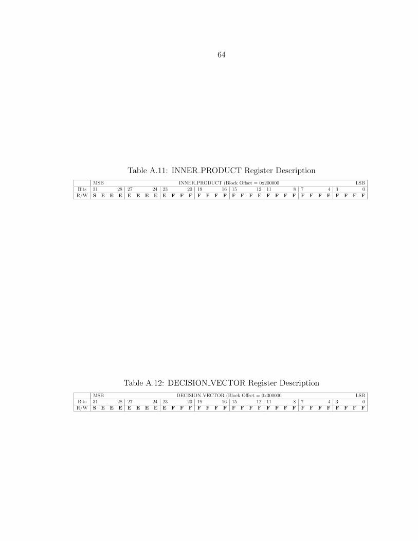
64
Table A.11: INNER PRODUCT Register Description
MSB INNER PRODUCT (Block Offset = 0x200000 LSBBits 31 28 27 24 23 20 19 16 15 12 11 8 7 4 3 0R/W S E E E E E E E E F F F F F F F F F F F F F F F F F F F F F F F
Table A.12: DECISION VECTOR Register Description
MSB DECISION VECTOR (Block Offset = 0x300000 LSBBits 31 28 27 24 23 20 19 16 15 12 11 8 7 4 3 0R/W S E E E E E E E E F F F F F F F F F F F F F F F F F F F F F F F

65
APPENDIX B
VHDL CODE

66
1 −−−−−−−−−−−−−−−−−−−−−−−−−−−−−−−−−−−−−−−−−−−−−−−−−−−−−−−−−−−−−2 −−3 −−! @ f i l e i 2 c d r i v e r . vhd4 −−! @br ie f Contro l s programming o f c l o c k genera tor over i2c5 −−! @de t a i l s Contains s t a t e machine f o r programming r e g i s t e r s
in6 −−! VersaClock c l o c k genera tor .7 −−! @author Monica Whitaker8 −−! @date September 20159 −−! @copyright Copyright (C) 2015 Ross K. Snider and Monica
Whitaker10 −−11 −− This program i s f r e e so f tware : you can r e d i s t r i b u t e i t and/or
modify12 −− i t under the terms o f the GNU General Pub l i c License as
pub l i s h ed by13 −− the Free Sof tware Foundation , e i t h e r ve r s i on 3 o f the License
, or14 −− ( a t your opt ion ) any l a t e r ve r s i on .15 −−16 −− This program i s d i s t r i b u t e d in the hope t ha t i t w i l l be
u s e fu l ,17 −− but WITHOUT ANY WARRANTY; wi thout even the imp l i ed warranty
o f18 −− MERCHANTABILITY or FITNESS FOR A PARTICULAR PURPOSE. See the19 −− GNU General Pub l i c License f o r more d e t a i l s .20 −−21 −− You shou ld have r e c e i v ed a copy o f the GNU General Pub l i c
License22 −− a long wi th t h i s program . I f not , see <h t t p ://www. gnu . org /
l i c e n s e s />.23 −−24 −− Monica Whitaker25 −− E l e c t r i c a l and Computer Engineer ing26 −− Montana S ta t e Un i v e r s i t y27 −− 610 Cob le i gh Ha l l28 −− Bozeman , MT 5971729 −− monica . whitaker@msu . montana . edu30 −−31 −−−−−−−−−−−−−−−−−−−−−−−−−−−−−−−−−−−−−−−−−−−−−−−−−−−−−−−−−−−−−32 l ibrary IEEE ; −−! Use standard l i b r a r y .33 use IEEE . STD LOGIC 1164 .ALL; −−! Use standard l o g i c e lements .34 use IEEE .NUMERIC STD.ALL; −−! Use numeric s tandard .35 −−−−−−−−−−−−−−−−−−−−−−−−−−−−−−−−−−−−−−−−−−−−−−−−−−−−−−−−−−−−−36 −−37 −−! @br ie f i 2 c d r i v e r

67
38 −−! @de t a i l s Contains s t a t e machine f o r programming r e g i s t e r sin
39 −−! VersaClock c l o c k genera tor .40 −−! @param c l k System c l o c k41 −−! @param re s e t n Reset s i g n a l42 −−! @param enab l e Enable s t a r t i n g s t a t e machine43 −−! @param i 2 c s c l Clock l i n e44 −−! @param i2c sda bi−d i r e c t i o n a l data l i n e45 −−! @param error I2C communication error46 −−! @param done Ind i c a t e s s t a t e machine complete47 −−! @param burn succes s S ta tus s i g n a l a f t e r burning
con f i g u ra t i on48 −−49 −−−−−−−−−−−−−−−−−−−−−−−−−−−−−−−−−−−−−−−−−−−−−−−−−−−−−−−−−−−−−50 entity i 2 c d r i v e r i s51 port (52 c l k : in s t d l o g i c ;53 r e s e t n : in s t d l o g i c ;54 enable : in s t d l o g i c ;55
56 i 2 c s c l : inout s t d l o g i c ;57 i 2 c s da : inout s t d l o g i c ;58
59 e r r o r : out s t d l o g i c ;60
61 done : out s t d l o g i c ;62 burn succe s s : out s t d l o g i c63 ) ;64 end entity ;65
66 architecture arch of i 2 c d r i v e r i s67 component i 2 c mas t e r i s68 GENERIC(69 i npu t c l k : INTEGER := 50 000 000 ; −−input c l o c k
speed (Hz)70 bus c l k : INTEGER := 400 000 ) ; −−speed o f s c l (Hz)71 PORT(72 c l k : IN STD LOGIC;73 r e s e t n : IN STD LOGIC;74 ena : IN STD LOGIC;75 addr : IN STD LOGIC VECTOR(6 DOWNTO 0) ;76 rw : IN STD LOGIC;77 data wr : IN STD LOGIC VECTOR(7 DOWNTO 0) ;78 busy : OUT STD LOGIC;79 data rd : OUT STD LOGIC VECTOR(7 DOWNTO 0) ;80 a ck e r r o r : BUFFER STD LOGIC;81 sda : INOUT STD LOGIC;

68
82 s c l : INOUT STD LOGIC83 ) ;84 end component ;85
86 −−address o f Clock Generator dev i c e87 −−xD4 (xD5 to read )88 constant addres s dev : s t d l o g i c v e c t o r (7 downto 0) :=89 "11010100" ;90
91 −−CONFIGURATION 0 HAS BEEN BURNED! !92 −−CHANGE Burn Reg i s t e r s f o r f u r t h e r burns93
94 −− Reg00 Name: RAM0 0095 −− Reg00 Descr ip t i on : OTP Contro l96 −− Hex Address = 0097 −− Defau l t = x”FF”98 constant Reg00 Addr : s t d l o g i c v e c t o r (7 downto 0) :=99 "00000000" ;
100 constant Reg00 Data : s t d l o g i c v e c t o r (7 downto 0) :=101 "01100001" ;102 −−−−−−−−−−−−−−−−−−−−−−−−−−−−−−−−−−−−−−−−−−−−−−−−−−−−−−−−−103 −− Reg01 Name: RAM1 XTAL1104 −− Reg01 Descr ip t i on : X1 Load Capaci tor105 −− Hex Address = 12106 −− Defau l t = 00000001107 constant Reg01 Addr : s t d l o g i c v e c t o r (7 downto 0) :=108 "00010010" ;109 constant Reg01 Data : s t d l o g i c v e c t o r (7 downto 0) :=110 "00101001" ;111 −−−−−−−−−−−−−−−−−−−−−−−−−−−−−−−−−−−−−−−−−−−−−−−−−−−−−−−−−112 −− Reg02 Name: RAM1 XTAL2113 −− Reg02 Descr ip t i on : Factory Reserved114 −− Hex Address = 13115 −− Defau l t = 00000000116 constant Reg02 Addr : s t d l o g i c v e c t o r (7 downto 0) :=117 "00010011" ;118 constant Reg02 Data : s t d l o g i c v e c t o r (7 downto 0) :=119 "00101000" ;120 −−−−−−−−−−−−−−−−−−−−−−−−−−−−−−−−−−−−−−−−−−−−−−−−−−−−−−−−−121 −− Reg03 Name: RAM1 Feedback122 −− Reg03 Descr ip t i on : Feedback In t e g e r Div ider (PLL)123 −− Hex Address = 17124 −− Defau l t = 00000011125 constant Reg03 Addr : s t d l o g i c v e c t o r (7 downto 0) :=126 "00010111" ;127 constant Reg03 Data : s t d l o g i c v e c t o r (7 downto 0) :=128 "00000110" ;

69
129 −−−−−−−−−−−−−−−−−−−−−−−−−−−−−−−−−−−−−−−−−−−−−−−−−−−−−−−−−130 −− Reg04 Name: RAM1 Feedback131 −− Reg04 Descr ip t i on : Feedback In t e g e r Div ider Bi t s (PLL)132 −− Hex Address = 18133 −− Defau l t = 00000000134 constant Reg04 Addr : s t d l o g i c v e c t o r (7 downto 0) :=135 "00011000" ;136 constant Reg04 Data : s t d l o g i c v e c t o r (7 downto 0) :=137 "01000000" ;138 −−−−−−−−−−−−−−−−−−−−−−−−−−−−−−−−−−−−−−−−−−−−−−−−−−−−−−−−−139 −− Reg05 Name: RAM2 2E140 −− Reg05 Descr ip t i on : Output Div ider In t e g e r 2141 −− Hex Address = 2e142 −− Defau l t = 11100000143 constant Reg05 Addr : s t d l o g i c v e c t o r (7 downto 0) :=144 "00101110" ;145 constant Reg05 Data : s t d l o g i c v e c t o r (7 downto 0) :=146 "10100000" ;147 −−−−−−−−−−−−−−−−−−−−−−−−−−−−−−−−−−−−−−−−−−−−−−−−−−−−−−−−−148 −− Reg06 Name: RAM6 60149 −− Reg06 Descr ip t i on : Clock1 Output Config150 −− Hex Address = 60151 −− Defau l t = 10111011152 constant Reg06 Addr : s t d l o g i c v e c t o r (7 downto 0) :=153 "01100000" ;154 constant Reg06 Data : s t d l o g i c v e c t o r (7 downto 0) :=155 "01111011" ;156 −−−−−−−−−−−−−−−−−−−−−−−−−−−−−−−−−−−−−−−−−−−−−−−−−−−−−−−−−157 −− Reg07 Name: RAM1 1D158 −− Reg07 Descr ip t i on : VCO Monitoring159 −− Hex Address = 1D160 −− Defau l t = 01101111161 constant Reg07 Addr : s t d l o g i c v e c t o r (7 downto 0) :=162 "00011101" ;163 constant Reg07 Data : s t d l o g i c v e c t o r (7 downto 0) :=164 "01001101" ;165 −−−−−−−−−−−−−−−−−−−−−−−−−−−−−−−−−−−−−−−−−−−−−−−−−−−−−−−−−166 −− Reg08 Name: RAM1 1E167 −− Reg08 Descr ip t i on : RC Contro l Reg i s t e r168 −− Hex Address = 1E169 −− Defau l t = 00000000170 constant Reg08 Addr : s t d l o g i c v e c t o r (7 downto 0) :=171 "00011110" ;172 constant Reg08 Data : s t d l o g i c v e c t o r (7 downto 0) :=173 "10010010" ;174 −−−−−−−−−−−−−−−−−−−−−−−−−−−−−−−−−−−−−−−−−−−−−−−−−−−−−−−−−175 −− Reg09 Name: RAM1 1F
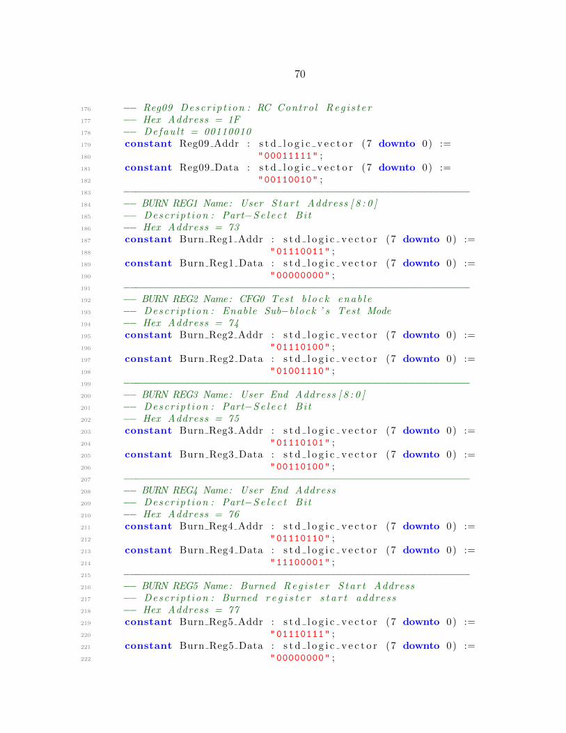
70
176 −− Reg09 Descr ip t i on : RC Contro l Reg i s t e r177 −− Hex Address = 1F178 −− Defau l t = 00110010179 constant Reg09 Addr : s t d l o g i c v e c t o r (7 downto 0) :=180 "00011111" ;181 constant Reg09 Data : s t d l o g i c v e c t o r (7 downto 0) :=182 "00110010" ;183 −−−−−−−−−−−−−−−−−−−−−−−−−−−−−−−−−−−−−−−−−−−−−−−−−−−−−−−−−184 −− BURN REG1 Name: User S t a r t Address [ 8 : 0 ]185 −− Descr ip t i on : Part−Se l e c t Bi t186 −− Hex Address = 73187 constant Burn Reg1 Addr : s t d l o g i c v e c t o r (7 downto 0) :=188 "01110011" ;189 constant Burn Reg1 Data : s t d l o g i c v e c t o r (7 downto 0) :=190 "00000000" ;191 −−−−−−−−−−−−−−−−−−−−−−−−−−−−−−−−−−−−−−−−−−−−−−−−−−−−−−−−−192 −− BURN REG2 Name: CFG0 Test b l o c k enab l e193 −− Descr ip t i on : Enable Sub−b lock ’ s Test Mode194 −− Hex Address = 74195 constant Burn Reg2 Addr : s t d l o g i c v e c t o r (7 downto 0) :=196 "01110100" ;197 constant Burn Reg2 Data : s t d l o g i c v e c t o r (7 downto 0) :=198 "01001110" ;199 −−−−−−−−−−−−−−−−−−−−−−−−−−−−−−−−−−−−−−−−−−−−−−−−−−−−−−−−−200 −− BURN REG3 Name: User End Address [ 8 : 0 ]201 −− Descr ip t i on : Part−Se l e c t Bi t202 −− Hex Address = 75203 constant Burn Reg3 Addr : s t d l o g i c v e c t o r (7 downto 0) :=204 "01110101" ;205 constant Burn Reg3 Data : s t d l o g i c v e c t o r (7 downto 0) :=206 "00110100" ;207 −−−−−−−−−−−−−−−−−−−−−−−−−−−−−−−−−−−−−−−−−−−−−−−−−−−−−−−−−208 −− BURN REG4 Name: User End Address209 −− Descr ip t i on : Part−Se l e c t Bi t210 −− Hex Address = 76211 constant Burn Reg4 Addr : s t d l o g i c v e c t o r (7 downto 0) :=212 "01110110" ;213 constant Burn Reg4 Data : s t d l o g i c v e c t o r (7 downto 0) :=214 "11100001" ;215 −−−−−−−−−−−−−−−−−−−−−−−−−−−−−−−−−−−−−−−−−−−−−−−−−−−−−−−−−216 −− BURN REG5 Name: Burned Reg i s t e r S t a r t Address217 −− Descr ip t i on : Burned r e g i s t e r s t a r t address218 −− Hex Address = 77219 constant Burn Reg5 Addr : s t d l o g i c v e c t o r (7 downto 0) :=220 "01110111" ;221 constant Burn Reg5 Data : s t d l o g i c v e c t o r (7 downto 0) :=222 "00000000" ;
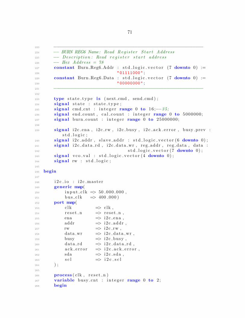
71
223 −−−−−−−−−−−−−−−−−−−−−−−−−−−−−−−−−−−−−−−−−−−−−−−−−−−−−−−−−224 −− BURN REG6 Name: Read Reg i s t e r S t a r t Address225 −− Descr ip t i on : Read r e g i s t e r s t a r t address226 −− Hex Address = 78227 constant Burn Reg6 Addr : s t d l o g i c v e c t o r (7 downto 0) :=228 "01111000" ;229 constant Burn Reg6 Data : s t d l o g i c v e c t o r (7 downto 0) :=230 "00000000" ;231 −−−−−−−−−−−−−−−−−−−−−−−−−−−−−−−−−−−−−−−−−−−−−−−−−−−−−−−−−232
233 type s t a t e t yp e i s ( next cmd , send cmd ) ;234 signal s t a t e : s t a t e t yp e ;235 signal cmd cnt : i n t e g e r range 0 to 16 ;−−35;236 signal end count , c a l c ount : i n t e g e r range 0 to 5000000;237 signal burn count : i n t e g e r range 0 to 25000000;238
239 signal i 2c ena , i2c rw , i2c busy , i 2 c a c k e r r o r , busy prev :s t d l o g i c ;
240 signal i 2c addr , s l ave addr : s t d l o g i c v e c t o r (6 downto 0) ;241 signal i 2 c da ta rd , i2c data wr , reg addr , reg data , data :242 s t d l o g i c v e c t o r (7 downto 0) ;243 signal vco va l : s t d l o g i c v e c t o r (4 downto 0) ;244 signal rw : s t d l o g i c ;245
246 begin247
248 i 2 c i o : i 2 c mas t e r249 generic map(250 i npu t c l k => 50 000 000 ,251 bus c l k => 400 000 )252 port map(253 c l k => c lk ,254 r e s e t n => r e s e t n ,255 ena => i 2c ena ,256 addr => i 2c addr ,257 rw => i2c rw ,258 data wr => i 2c data wr ,259 busy => i 2c busy ,260 data rd => i 2 c da ta rd ,261 a ck e r r o r => i 2 c a c k e r r o r ,262 sda => i 2 c sda ,263 s c l => i 2 c s c l264 ) ;265
266 process ( c lk , r e s e t n )267 variable busy cnt : i n t e g e r range 0 to 2 ;268 begin

72
269 i f ( r e s e t n = ’0 ’ ) then270 busy cnt := 0 ;271 done <= ’0 ’ ;272 s t a t e <= next cmd ;273 i 2 c ena <= ’0 ’ ;274 end count <= 0 ;275 ca l c ount <= 0 ;276 cmd cnt <= 0 ;277 e r r o r <= ’0 ’ ;278 burn count <= 0 ;279 e l s i f ( r i s i n g e d g e ( c l k ) ) then280 i f ( enable = ’1 ’ ) then281 case s t a t e i s282 when send cmd =>283 −− l a t c h busy s i g n a l284 busy prev <= i2c busy ;285 i f ( busy prev = ’0 ’ and i 2 c busy = ’1 ’ )
then286 busy cnt := busy cnt + 1 ;287 end i f ;288
289 case busy cnt i s290 when 0 =>291 i 2 c ena <= ’1 ’ ;292 i 2 c addr <= s lave addr ;293 −−always wr i t e f i r s t294 i 2 c rw <= ’0 ’ ;295 i 2 c da ta wr <= reg addr ;296 when 1 =>297 i f ( rw = ’1 ’ ) then298 −− i f reading , do so299 i 2 c rw <= rw ;300 else −−otherwise , wr i t e data301 i 2 c da ta wr <= reg data ;302 end i f ;303 when 2 =>304 i 2 c ena <= ’0 ’ ;305 i f ( i 2 c busy = ’0 ’ ) then306 −−c o l l e c t data read307 data <= i2 c da t a rd ;308 busy cnt := 0 ;309 s t a t e <= next cmd ;310 end i f ;311 end case ;312
313 when next cmd =>314 −−Burn process has known p o s s i b i l i t y

73
315 −−o f NAK316 −− i f ( i 2 c a c k e r r o r = ’1 ’ and cmd cnt /= 0)317 −− then318 −− −−s t a t e <= send cmd ;319 −− error <= ’1 ’ ;320 −− e l s e321 case cmd cnt i s322 when 0 =>323 s l ave addr <= address dev (7
downto 1) ;324 rw <= ’0 ’ ; −−wr i t e325 reg addr <= Reg01 Addr ;326 r eg data <= Reg01 Data ;327 cmd cnt <= 1 ;328 s t a t e <= send cmd ;329 when 1 =>330 reg addr <= Reg02 Addr ;331 r eg data <= Reg02 Data ;332 cmd cnt <= 2 ;333 s t a t e <= send cmd ;334 when 2 =>335 reg addr <= Reg03 Addr ;336 r eg data <= Reg03 Data ;337 cmd cnt <= 3 ;338 s t a t e <= send cmd ;339 when 3 =>340 reg addr <= Reg04 Addr ;341 r eg data <= Reg04 Data ;342 cmd cnt <= 4 ;343 s t a t e <= send cmd ;344 when 4 =>345 reg addr <= Reg05 Addr ;346 r eg data <= Reg05 Data ;347 cmd cnt <= 5 ;348 s t a t e <= send cmd ;349 when 5 =>350 reg addr <= Reg06 Addr ;351 r eg data <= Reg06 Data ;352 cmd cnt <= 6 ;353 s t a t e <= send cmd ;354 when 6 =>355 reg addr <= Reg07 Addr ;356 r eg data <= Reg07 Data ;357 cmd cnt <= 7 ;358 s t a t e <= send cmd ;359 when 7 =>360 reg addr <= Reg08 Addr ;

74
361 r eg data <= Reg08 Data ;362 cmd cnt <= 8 ;363 s t a t e <= send cmd ;364 when 8 =>365 reg addr <= Reg09 Addr ;366 r eg data <= Reg09 Data ;367 cmd cnt <= 9 ;368 s t a t e <= send cmd ;369 when 9 => −−Begin VCO ca l i b r a t i o n370 reg addr <= x"11" ;371 r eg data <= "00001100" ;372 cmd cnt <= 10 ;373 s t a t e <= send cmd ;374 when 10 => −−t o g g l e b i t 7375 reg addr <= x"1C" ;376 r eg data <= "00000101" ;377 rw <= ’0 ’ ;378 cmd cnt <= 11 ;379 s t a t e <= send cmd ;380 when 11 =>381 reg addr <= x"1C" ;382 r eg data <= "10000101" ;383 cmd cnt <= 12 ;384 s t a t e <= send cmd ;385 when 12 =>386 reg addr <= x"1C" ;387 r eg data <= "00000101" ;388 cmd cnt <= 13 ;389 s t a t e <= send cmd ;390 when 13 => −−wai t 100ms391 i f ( ca l c ount = 5000000) then392 ca l c ount <= 0 ;393 reg addr <= x"99" ;394 rw <= ’1 ’ ; −−
read395 cmd cnt <= 14 ;396 s t a t e <= send cmd ;397 else398 ca l c ount <= ca l count +
1 ;399 end i f ;400 when 14 =>401 −−s t o r e data read from
r e g i s t e r402 vco va l <= data (7 downto 3) ;403 cmd cnt <= 15 ;404 when 15 =>
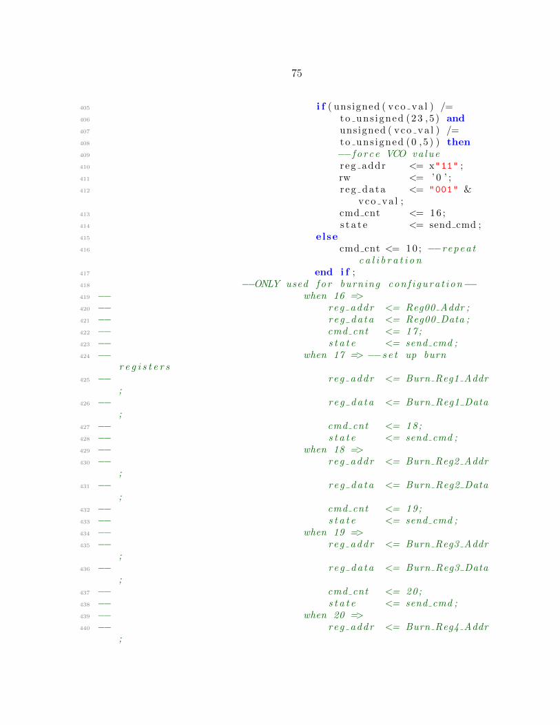
75
405 i f ( unsigned ( vco va l ) /=406 to uns igned (23 ,5 ) and407 unsigned ( vco va l ) /=408 to uns igned (0 , 5 ) ) then409 −−f o r c e VCO va lue410 reg addr <= x"11" ;411 rw <= ’0 ’ ;412 r eg data <= "001" &
vco va l ;413 cmd cnt <= 16 ;414 s t a t e <= send cmd ;415 else416 cmd cnt <= 10 ; −−repea t
c a l i b r a t i o n417 end i f ;418 −−ONLY used f o r burning con f i gura t i on−−419 −− when 16 =>420 −− reg addr <= Reg00 Addr ;421 −− r e g da ta <= Reg00 Data ;422 −− cmd cnt <= 17;423 −− s t a t e <= send cmd ;424 −− when 17 => −−s e t up burn
r e g i s t e r s425 −− reg addr <= Burn Reg1 Addr
;426 −− r e g da ta <= Burn Reg1 Data
;427 −− cmd cnt <= 18;428 −− s t a t e <= send cmd ;429 −− when 18 =>430 −− reg addr <= Burn Reg2 Addr
;431 −− r e g da ta <= Burn Reg2 Data
;432 −− cmd cnt <= 19;433 −− s t a t e <= send cmd ;434 −− when 19 =>435 −− reg addr <= Burn Reg3 Addr
;436 −− r e g da ta <= Burn Reg3 Data
;437 −− cmd cnt <= 20;438 −− s t a t e <= send cmd ;439 −− when 20 =>440 −− reg addr <= Burn Reg4 Addr
;

76
441 −− r e g da ta <= Burn Reg4 Data;
442 −− cmd cnt <= 21;443 −− s t a t e <= send cmd ;444 −− when 21 =>445 −− reg addr <= Burn Reg5 Addr
;446 −− r e g da ta <= Burn Reg5 Data
;447 −− cmd cnt <= 22;448 −− s t a t e <= send cmd ;449 −− when 22 =>450 −− reg addr <= Burn Reg6 Addr
;451 −− r e g da ta <= Burn Reg6 Data
;452 −− cmd cnt <= 23;453 −− s t a t e <= send cmd ;454 −− when 23 =>455 −− −−wai t 100ms456 −− i f ( end count = 5000000)
then457 −− cmd cnt <= 24;458 −− e l s e459 −− end count <= end count
+ 1;460 −− end i f ;461 −− when 24 => −−s t a r t burn proces s462 −− reg addr <= x ”72”;463 −− r e g da ta <= x”F0”;464 −− cmd cnt <= 25;465 −− s t a t e <= send cmd ;466 −− when 25 =>467 −− reg addr <= x ”72”;468 −− r e g da ta <= x”F8”;469 −− cmd cnt <= 26;470 −− s t a t e <= send cmd ;471 −− when 26 =>472 −− −−wai t 500ms473 −− i f ( burn count = 25000000)
then474 −− cmd cnt <= 27;475 −− burn count <= 0;476 −− e l s e477 −− burn count <=
burn count + 1;478 −− end i f ;
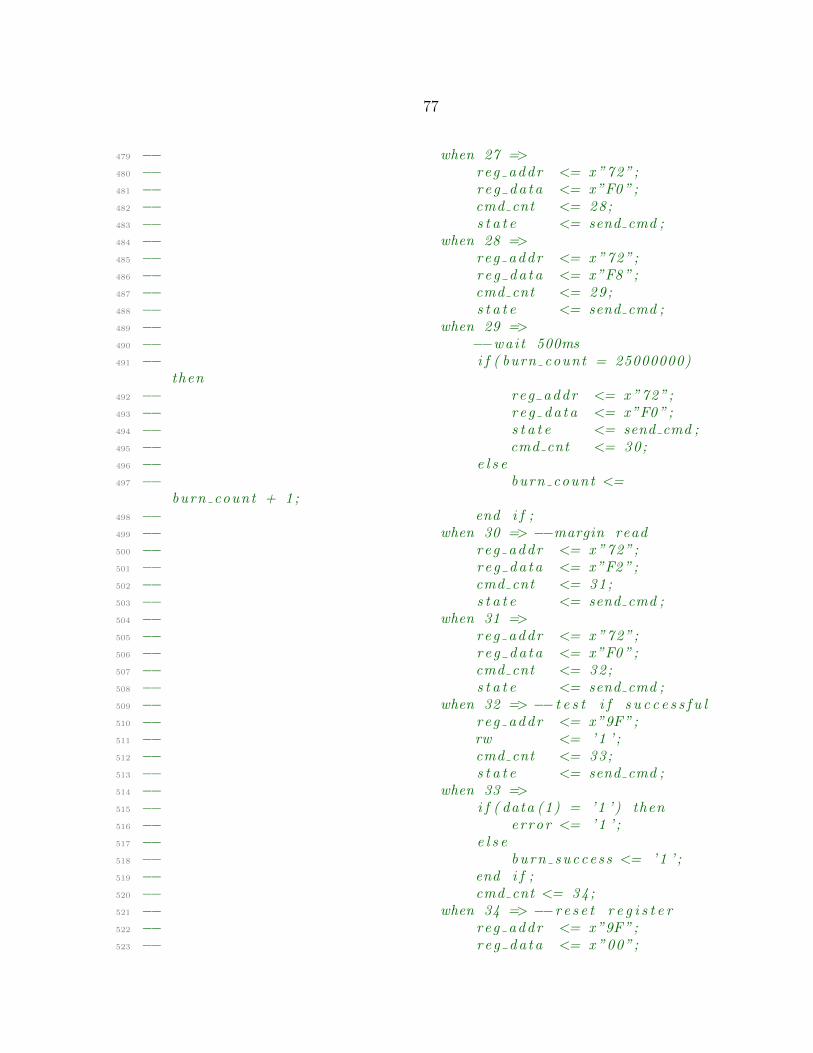
77
479 −− when 27 =>480 −− reg addr <= x ”72”;481 −− r e g da ta <= x”F0”;482 −− cmd cnt <= 28;483 −− s t a t e <= send cmd ;484 −− when 28 =>485 −− reg addr <= x ”72”;486 −− r e g da ta <= x”F8”;487 −− cmd cnt <= 29;488 −− s t a t e <= send cmd ;489 −− when 29 =>490 −− −−wai t 500ms491 −− i f ( burn count = 25000000)
then492 −− reg addr <= x ”72”;493 −− r e g da ta <= x”F0”;494 −− s t a t e <= send cmd ;495 −− cmd cnt <= 30;496 −− e l s e497 −− burn count <=
burn count + 1;498 −− end i f ;499 −− when 30 => −−margin read500 −− reg addr <= x ”72”;501 −− r e g da ta <= x”F2”;502 −− cmd cnt <= 31;503 −− s t a t e <= send cmd ;504 −− when 31 =>505 −− reg addr <= x ”72”;506 −− r e g da ta <= x”F0”;507 −− cmd cnt <= 32;508 −− s t a t e <= send cmd ;509 −− when 32 => −− t e s t i f s u c c e s s f u l510 −− reg addr <= x”9F”;511 −− rw <= ’1 ’ ;512 −− cmd cnt <= 33;513 −− s t a t e <= send cmd ;514 −− when 33 =>515 −− i f ( data (1) = ’1 ’ ) then516 −− error <= ’1 ’ ;517 −− e l s e518 −− burn succes s <= ’1 ’ ;519 −− end i f ;520 −− cmd cnt <= 34;521 −− when 34 => −−r e s e t r e g i s t e r522 −− reg addr <= x”9F”;523 −− r e g da ta <= x ”00”;

78
524 −− rw <= ’0 ’ ;525 −− cmd cnt <= 35;526 −− s t a t e <= send cmd ;527 when 16 =>−−35 =>528 done <= ’1 ’ ;529 end case ;530 −− end i f ;531 end case ;532 end i f ;533 end i f ;534 end process ;535 end architecture ;
1 −−−−−−−−−−−−−−−−−−−−−−−−−−−−−−−−−−−−−−−−−−−−−−−−−−−−−−−−−−−−−2 −−3 −−! @ f i l e r e g r e s s i on . vhd4 −−! @br ie f The l o g i s t i c r e g r e s s i on computation un i t .5 −−! @de t a i l s Computes the s t a t i s t i c a l p r o b a b i l i t y o f a p i x e l6 −−! b e l ong ing to a p a r t i c u l a r c l a s s g i ven s e v e r a l7 −−! d i f f e r e n t c l a s s c o e f f i c i e n t s and normal ized p i x e l8 −−! data .9 −−! @author Monica Whitaker
10 −−! @date September 201511 −−! @copyright Copyright (C) 2015 Ross K. Snider and12 −−! Monica Whitaker13 −−14 −− This program i s f r e e so f tware : you can r e d i s t r i b u t e i t and/or15 −− modify i t under the terms o f the GNU General Pub l i c License16 −− as pub l i s h ed by the Free Sof tware Foundation , e i t h e r ve r s i on17 −− 3 o f the License , or ( at your opt ion ) any l a t e r ve r s i on .18 −−19 −− This program i s d i s t r i b u t e d in the hope t ha t i t w i l l be20 −− use fu l , but WITHOUT ANY WARRANTY; wi thout even the imp l i ed21 −− warranty o f MERCHANTABILITY or FITNESS FOR A PARTICULAR22 −− PURPOSE. See the GNU General Pub l i c License f o r more d e t a i l s .23 −−24 −− You shou ld have r e c e i v ed a copy o f the GNU General Pub l i c25 −− License a long wi th t h i s program . I f not , see <h t t p ://www. gnu
. org / l i c e n s e s />.26 −−27 −− Monica Whitaker28 −− E l e c t r i c a l and Computer Engineer ing29 −− Montana S ta t e Un i v e r s i t y30 −− 610 Cob le i gh Ha l l31 −− Bozeman , MT 5971732 −− monica . whitaker@msu . montana . edu33 −−

79
34 −−−−−−−−−−−−−−−−−−−−−−−−−−−−−−−−−−−−−−−−−−−−−−−−−−−−−−−−−−−−−35 l ibrary IEEE ; −−! Use standard l i b r a r y .36 use IEEE . STD LOGIC 1164 .ALL; −−! Use standard l o g i c e lements .37 use IEEE .NUMERIC STD.ALL; −−! Use numeric s tandard .38 use IEEE .MATHREAL.ALL; −−! Use r e a l math l i b r a r y39
40 use work . Sensor Package . a l l ; −−! Pro jec t cons tan t s package41 −−−−−−−−−−−−−−−−−−−−−−−−−−−−−−−−−−−−−−−−−−−−−−−−−−−−−−−−−−−−−42 −−43 −−! @br ie f r e g r e s s i on44 −−! @de t a i l s Computes the s t a t i s t i c a l p r o b a b i l i t y o f a p i x e l45 −−! b e l ong ing to a p a r t i c u l a r c l a s s g i ven s e v e r a l46 −−! d i f f e r e n t c l a s s c o e f f i c i e n t s and normal ized p i x e l47 −−! data .48 −−! @param TOTAL INPUT SIZE Si ze o f a l l p a r a l l e l
p i x e l data .49 −−! @param WORD SIZE Standard word s i z e50 −−! @param i n p u t c l k P i x e l c l o c k51 −−! @param enab l e i n Enable s i g n a l from HPS52 −−! @param s u p e r p i x e l i n Vector o f a l l r e l e v an t
p i x e l in format ion f o r each p a r a l l e l channel53 −−! @param p i x e l r e s u l t s o u t Vector o f p r o b a b i l i t i e s
and p i x e l number54 −−! @param p i x e l r e s u l t s f l a g o u t Flag i n d i c a t i n g new
r e s u l t s on output55 −−! @param f r ame f l a g ou t Flag to i n d i c a t e new
frame56 −−! @param f a s t c l k Clock running at t r i p l e
the speed o f57 −−! the input c l o c k58 −−! @param hp s c l k Clock f o r s i g n a l s from
HPS59 −−! @param r s t n System ac t i v e−low r e s e t
s i g n a l60 −−! @param da t a v a l i d i n Ind i c a t e s new data
presen t on61 −−! s u p e r p i x e l i n62 −−! @param c l e a r p i x e l i n Ind i c a t e s bad p i x e l and
t r i g g e r to c l e a r the cu r r en t l y p roce s s ing p i x e l when high63 −−! @param avs s1 r ead Read r e que s t from HPS64 −−! @param av s s 1 w r i t e Write r e que s t from HPS65 −−! @param av s s1 add r e s s Data address from HPS66 −−! @param avs s1 r eadda ta Output data f o r HPS67 −−! @param av s s 1 wr i t e d a t a Input data from HPS68 −−69 −−−−−−−−−−−−−−−−−−−−−−−−−−−−−−−−−−−−−−−−−−−−−−−−−−−−−−−−−−−−−70 entity r e g r e s s i o n i s
80
71 generic (72 TOTAL INPUT SIZE : natura l :=73 NUMBEROF PARALLEL CHANNELS ∗ SUPER PIXEL SIZE ;74 WORD SIZE : natura l := 3275 ) ;76 port (77 i npu t c l k : in s t d l o g i c ;78 enab l e i n : in s t d l o g i c ;79 s u p e r p i x e l i n : in s t d l o g i c v e c t o r (
TOTAL INPUT SIZE − 1 downto 0) ;80 p i x e l r e s u l t s o u t : out s t d l o g i c v e c t o r (
NUMBER OF CLASSES∗WORD SIZE+PIXEL ADDRESS SIZE − 1downto 0) ;
81 p i x e l r e s u l t s f l a g o u t : out s t d l o g i c ;82 f a s t c l k : in s t d l o g i c ;83 hps c l k : in s t d l o g i c ;84 hp s r e s e t : in s t d l o g i c ;85 r s t n : in s t d l o g i c ;86 da t a v a l i d i n : in s t d l o g i c ;87 c l e a r p i x e l i n : in s t d l o g i c ;88
89 av s s 1 r ead : in s t d l o g i c ;90 av s s 1 w r i t e : in s t d l o g i c ;91 av s s 1 add r e s s : in s t d l o g i c v e c t o r (31 downto
0) ;92 avs s1 r eaddata : out s t d l o g i c v e c t o r (31 downto
0) ;93 av s s 1 wr i t eda ta : in s t d l o g i c v e c t o r (31 downto
0)94 ) ;95 end entity ;96
97 architecture r t l of r e g r e s s i o n i s98
99 −−−−−−−−−−−−−−−−−−−−−−−−−−−−−−−−−−−−−−−−−−−−−−−−−−−−−−−−−−−−−100 −− Component De f i n i t i o n s101 −−−−−−−−−−−−−−−−−−−−−−−−−−−−−−−−−−−−−−−−−−−−−−−−−−−−−−−−−−−−−102 component normal ize i s −−15 c y c l e l a t ency103 port (104 c l k : in s t d l o g i c ;105 r s t n : in s t d l o g i c ;106 da t a v a l i d i n : in s t d l o g i c ;107 data in : in s t d l o g i c v e c t o r (31 downto 0) ;108 dark in : in s t d l o g i c v e c t o r (31 downto 0) ;109 l i g h t I i n : in s t d l o g i c v e c t o r (31 downto 0) ;110 mean in : in s t d l o g i c v e c t o r (31 downto 0) ;111 s t ddev I i n : in s t d l o g i c v e c t o r (31 downto 0) ;
81
112 normal i zed out : out s t d l o g i c v e c t o r (31 downto 0)113 ) ;114 end component normal ize ;115
116 component f p mu l t acc i s −−4 c y c l e s117 port (118 a : in s t d l o g i c v e c t o r (31 downto 0) :=119 ( others => ’ 0 ’ ) ;120 acc : in s t d l o g i c := ’ 0 ’ ;121 a r e s e t : in s t d l o g i c := ’ 0 ’ ;122 b : in s t d l o g i c v e c t o r (31 downto 0) :=123 ( others => ’ 0 ’ ) ;124 c l k : in s t d l o g i c := ’ 0 ’ ;125 q : out s t d l o g i c v e c t o r (31 downto 0)126 ) ;127 end component ;128
129 component memory block i s130 generic (131 num elements a : natura l ;132 num elements b : natura l ;133 s i z e a dd r e s s a : natura l ;134 s i z e a dd r e s s b : natura l ;135 s i z e word a : natura l ;136 s i z e word b : natura l ;137 mem init : s t r i n g := "UNUSED"
138 ) ;139 port (140 addre s s a : in s t d l o g i c v e c t o r ( s i z e add r e s s a −1
downto 0) ;141 addres s b : in s t d l o g i c v e c t o r ( s i z e add r e s s b −1
downto 0) ;142 c l o ck a : in s t d l o g i c := ’ 1 ’ ;143 c l o ck b : in s t d l o g i c := ’ 1 ’ ;144 data a : in s t d l o g i c v e c t o r ( s i z e word a−1
downto 0) ;145 data b : in s t d l o g i c v e c t o r ( s i ze word b−1
downto 0) ;146 wren a : in s t d l o g i c := ’ 0 ’ ;147 wren b : in s t d l o g i c := ’ 0 ’ ;148 q a : out s t d l o g i c v e c t o r ( s i z e word a−1 downto
0) ;149 q b : out s t d l o g i c v e c t o r ( s i ze word b−1 downto
0)150 ) ;151 end component memory block ;152

82
153 component f i x e d t o f l o a t i s −−2 c y c l e s154 port (155 a : in s t d l o g i c v e c t o r (15 downto 0) :=156 ( others => ’ 0 ’ ) ;157 a r e s e t : in s t d l o g i c := ’ 0 ’ ;158 c l k : in s t d l o g i c := ’ 0 ’ ;159 q : out s t d l o g i c v e c t o r (31 downto 0)160 ) ;161 end component f i x e d t o f l o a t ;162
163 component channel sum i s164 generic (165 WORD SIZE : natura l := 32166 ) ;167 port (168 c l k : in s t d l o g i c ;169 f a s t c l k : in s t d l o g i c ;170 r s t n : in s t d l o g i c ;171 i n t e r c e p t i n : in s t d l o g i c v e c t o r (WORD SIZE−1
downto 0) ;172 data in : in s t d l o g i c v e c t o r (173 NUMBEROF PARALLEL CHANNELS∗
WORD SIZE−1 downto 0) ;174 r e s u l t o u t : out s t d l o g i c v e c t o r (WORD SIZE−1
downto 0)175 ) ;176 end component ;177 −−−−−−−−−−−−−−−−−−−−−−−−−−−−−−−−−−−−−−−−−−−−−−−−−−−−−−−−−−−−−178 −− Constant De f i n i t i o n s179 −−−−−−−−−−−−−−−−−−−−−−−−−−−−−−−−−−−−−−−−−−−−−−−−−−−−−−−−−−−−−180 −−v a l i d va l u e s = 1 , 2 , 4 , 8 , 16181 constant PSEUDO PARALLEL CHANNELS : natura l := 8 ;182
183 constant MEMORYWORDSHPS : natura l :=184 (NUMBER OF SPECTRAL BINS/
NUMBEROF PARALLEL CHANNELS) ∗185 PSEUDO PARALLEL CHANNELS;186 constant HPS MEM ADDR SIZE : natura l := natura l ( l og2
( r e a l (MEMORYWORDSHPS) ) ) ;187
188 constant CONVERSION LEVELS : natura l := 3 ;189 constant NORMALIZE LEVELS : natura l := 15 ;190 constant PRODUCT LEVELS : natura l := 4 ;191 −−3 c y c l e s per add192 constant COMBINATION LEVELS : natura l := 2∗(
NUMBEROF PARALLEL CHANNELS) ;
83
193 constant NUMBER LEVELS : natura l :=CONVERSION LEVELS + NORMALIZE LEVELS + PRODUCT LEVELS +COMBINATION LEVELS + 2 ;
194
195 constant ZEROS : s t d l o g i c v e c t o r (31downto 0) := x"00000000" ;
196 −−−−−−−−−−−−−−−−−−−−−−−−−−−−−−−−−−−−−−−−−−−−−−−−−−−−−−−−−−−−−197 −− Type De f i n i t i o n s198 −−−−−−−−−−−−−−−−−−−−−−−−−−−−−−−−−−−−−−−−−−−−−−−−−−−−−−−−−−−−−199 type wr i t e a r r ay i s array (1 to NUMBER OF CLASSES) of
s t d l o g i c ;200 type word array i s array (1 to NUMBER OF CLASSES) of201 s t d l o g i c v e c t o r (WORD SIZE − 1
downto 0) ;202 type c l a s s a r r a y i s array (1 to NUMBER OF CLASSES) of203 s t d l o g i c v e c t o r (WORD SIZE∗204 PSEUDO PARALLEL CHANNELS − 1
downto 0) ;205
206 type row array i s array (1 toNUMBEROF PARALLEL CHANNELS) of s t d l o g i c v e c t o r (SPECTRAL BIN ADDRESS SIZE − 1 downto 0) ;
207 type column array i s array (1 toNUMBEROF PARALLEL CHANNELS) of s t d l o g i c v e c t o r (PIXEL ADDRESS SIZE − 1 downto 0) ;
208 type i n da t a a r r ay i s array (1 toNUMBEROF PARALLEL CHANNELS) of s t d l o g i c v e c t o r (DATA SIZE− 1 downto 0) ;
209 type data ar ray i s array (1 toNUMBEROF PARALLEL CHANNELS) of s t d l o g i c v e c t o r (WORD SIZE− 1 downto 0) ;
210 type p a r t i a l s a r r a y i s array (1 to NUMBER OF CLASSES) ofdata ar ray ;
211 type product ar ray i s array (1 to NUMBER OF CLASSES) ofs t d l o g i c v e c t o r (NUMBEROF PARALLEL CHANNELS∗
WORD SIZE − 1 downto 0) ;212
213 type prod array i s array (1 toNUMBEROF PARALLEL CHANNELS) of s t d l o g i c ;
214 type p rod s i g a r r ay i s array (1 to NUMBER OF CLASSES) ofprod array ;
215
216 type d a t a l e v e l s a r r a y i s array (1 to NUMBER LEVELS) ofdata ar ray ;
217 type b in s a r r ay i s array (1 to NUMBER LEVELS) ofrow array ;

84
218 type p i x e l s a r r a y i s array (1 to NUMBER LEVELS) ofcolumn array ;
219 type l o g i c a r r a y i s array (1 to NUMBER LEVELS) ofs t d l o g i c ;
220 type mem addr array i s array (1 to NUMBER LEVELS) ofs t d l o g i c v e c t o r ( natura l ( trunc ( log2 ( r e a l (
NUMBER OF SPECTRAL BINS /NUMBEROF PARALLEL CHANNELS) ) ) )−1 downto 0) ;
221 −−−−−−−−−−−−−−−−−−−−−−−−−−−−−−−−−−−−−−−−−−−−−−−−−−−−−−−−−−−−−222 −− S igna l De f i n i t i o n s223 −−−−−−−−−−−−−−−−−−−−−−−−−−−−−−−−−−−−−−−−−−−−−−−−−−−−−−−−−−−−−224 signal da ta c l k : s t d l o g i c ;225 signal r e s e t : s t d l o g i c ;226 signal mean write : s t d l o g i c ;227 signal s tddev I wr i t e : s t d l o g i c ;228
229 signal va l id , p i x e l e r r : l o g i c a r r a y ;230
231 signal row0 : row array ;232 signal column0 : column array ;233 signal bin : b i n s a r r ay ;234 signal p i x e l : p i x e l s a r r a y ;235 signal mem address : mem addr array ;236 signal da t a f l o a t : data ar ray ;237 signal normal : data ar ray ;238 signal data : i n da t a a r r ay ;239 signal l i g h t I : d a t a l e v e l s a r r a y ;240 signal dark : d a t a l e v e l s a r r a y ;241 signal c l a s s , c l a s s s i g : c l a s s a r r a y ;242
243 signal i n t e r c e p t s : word array ;244 signal r e s u l t s : word array ;245 signal r e su l t s t emp : word array ;246 signal r e a d c l a s s : word array ;247 signal r e ad i n t e r c e p t : word array ;248 signal r e a d r e s u l t : word array ;249 signal z e r o a r r ay : word array :=250 ( others => x"00000000" ) ;251
252 signal p a r t i a l : p a r t i a l s a r r a y ;253
254 signal f i n a l p a r t i a l : p roduct ar ray ;255
256 signal c l a s s w r i t e : w r i t e a r r ay ;257 signal i n t e r c e p t w r i t e : w r i t e a r r ay ;258 signal r e s u l t w r i t e : w r i t e a r r ay ;259

85
260 signal acc : p r od s i g a r r ay ;261
262 signal mean : s t d l o g i c v e c t o r (PSEUDO PARALLEL CHANNELS∗ WORD SIZE − 1 downto 0) ;
263 signal s tddevI : s t d l o g i c v e c t o r (PSEUDO PARALLEL CHANNELS∗ WORD SIZE − 1 downto 0) ;
264
265 signal c l a s s add r : s t d l o g i c v e c t o r (HPS MEM ADDR SIZE−1 downto 0) ;
266 signal mean addr : s t d l o g i c v e c t o r (HPS MEM ADDR SIZE−1 downto 0) ;
267 signal stddev addr : s t d l o g i c v e c t o r (HPS MEM ADDR SIZE−1 downto 0) ;
268
269 signal read mean : s t d l o g i c v e c t o r (WORD SIZE − 1downto 0) ;
270 signal r ead s tddev I : s t d l o g i c v e c t o r (WORD SIZE − 1downto 0) ;
271
272 begin273
274 −− l a s t b in o f p i x e l has f i n i s h e d proce s s ing275 p i x e l r e s u l t s f l a g o u t <= ’1 ’ when ( bin (NUMBER LEVELS) (
NUMBEROF PARALLEL CHANNELS) = s t d l o g i c v e c t o r (to uns igned (NUMBER OF SPECTRAL BINS−1,SPECTRAL BIN ADDRESS SIZE) ) ) else ’ 0 ’ ;
276
277 i memory block means : memory block −−fpga on b , hps on a278 generic map(279 num elements a => MEMORYWORDSHPS,280 num elements b => NUMBER OF SPECTRAL BINS /281 NUMBER OF PARALLEL CHANNELS,282 s i z e a dd r e s s a => HPS MEM ADDR SIZE,283 s i z e a dd r e s s b => natura l ( trunc ( log2 ( r e a l (
NUMBER OF SPECTRAL BINS /284 NUMBEROF PARALLEL CHANNELS) ) ) ) ,285 s i z e word a => WORD SIZE,286 s i z e word b => PSEUDO PARALLEL CHANNELS ∗ WORD SIZE,287 mem init => "means.mif"
288 )289 port map(290 addre s s a => mean addr ,291 addres s b => mem address (CONVERSION LEVELS − 1) ,292 c l o ck a => hps c lk ,293 c l o ck b => data c lk ,294 data a => avs s1 wr i t eda ta ,295 data b => ( others => ’ 0 ’ ) ,
86
296 wren a => mean write ,297 wren b => ’ 0 ’ ,298 q a => read mean ,299 q b => mean300 ) ;301
302 mean addr <= avs s 1 add r e s s (HPS MEM ADDR SIZE−1 downto 0)when av s s 1 add r e s s (10) = ’ 1 ’ ;
303
304 i memory block stddevs : memory block −−read on b , wr i t e on a305 generic map(306 num elements a => MEMORYWORDSHPS,307 num elements b => NUMBER OF SPECTRAL BINS /308 NUMBER OF PARALLEL CHANNELS,309 s i z e a dd r e s s a => HPS MEM ADDR SIZE,310 s i z e a dd r e s s b => natura l ( trunc ( log2 ( r e a l (
NUMBER OF SPECTRAL BINS /311 NUMBEROF PARALLEL CHANNELS) ) ) ) ,312 s i z e word a => WORD SIZE,313 s i z e word b => PSEUDO PARALLEL CHANNELS ∗ WORD SIZE,314 mem init => "stddevs.mif"
315 )316 port map(317 addre s s a => stddev addr ,318 addres s b => mem address (CONVERSION LEVELS − 1) ,319 c l o ck a => hps c lk ,320 c l o ck b => data c lk ,321 data a => avs s1 wr i t eda ta ,322 data b => ( others => ’ 0 ’ ) ,323 wren a => s tddev I wr i t e ,324 wren b => ’ 0 ’ ,325 q a => read stddevI ,326 q b => s tddevI327 ) ;328
329 stddev addr <= avs s 1 add r e s s (HPS MEM ADDR SIZE−1 downto 0)when av s s 1 add r e s s (12) = ’ 1 ’ ;
330
331 g normal i ze : for j in 1 to NUMBEROF PARALLEL CHANNELSgenerate
332
333 i f i x e d t o f l o a t : f i x e d t o f l o a t334 port map(335 a => data ( j ) ,336 a r e s e t => r e s e t ,337 c l k => data c lk ,338 q => da t a f l o a t ( j )
87
339 ) ;340
341 −−normal ize by l i g h t , dark , mean , s tddev342 i n o rma l i z e : normal ize343 port map(344 c l k => data c lk ,345 r s t n => r s t n ,346 da t a v a l i d i n => va l i d (CONVERSION LEVELS) ,347 data in => da t a f l o a t ( j ) ,348 dark in => dark (CONVERSION LEVELS) ( j ) ,349 l i g h t I i n => l i g h t I (CONVERSION LEVELS) ( j ) ,350 mean in => mean(WORD SIZE∗ j−1 downto
WORD SIZE∗( j−1) ) ,351 s t ddev I i n => s tddevI (WORD SIZE∗ j−1 downto
WORD SIZE∗( j−1) ) ,352 normal i zed out => normal ( j )353 ) ;354
355 end generate ;356
357 c l a s s add r <= s t d l o g i c v e c t o r ( unsigned ( av s s 1 add r e s s (358 HPS MEM ADDR SIZE−1 downto 0) ) − 1) ;359
360 g c l a s s i f y : for i in 1 to NUMBER OF CLASSES generate361
362 i memory b l o ck in t e r c ep t s : memory block363 generic map(364 num elements a => 1 ,365 num elements b => 1 ,366 s i z e a dd r e s s a => 1 ,367 s i z e a dd r e s s b => 1 ,368 s i z e word a => WORD SIZE,369 s i z e word b => WORD SIZE,370 mem init => "UNUSED"
371 )372 port map(373 addre s s a => "0" ,374 addres s b => "0" ,375 c l o ck a => data c lk ,376 c l o ck b => hps c lk ,377 data a => ( others => ’ 0 ’ ) ,378 data b => avs s1 wr i t eda ta ,379 wren a => ’ 0 ’ ,380 wren b => i n t e r c e p t w r i t e ( i ) ,381 q a => i n t e r c e p t s ( i ) ,382 q b => r e ad i n t e r c e p t ( i )383 ) ;

88
384
385 i memory b l o ck c l a s s e s : memory block −−FPGA on b , HPS ona
386 generic map(387 num elements a => MEMORYWORDSHPS,388 num elements b => NUMBER OF SPECTRAL BINS /389 NUMBER OF PARALLEL CHANNELS,390 s i z e a dd r e s s a => HPS MEM ADDR SIZE,391 s i z e a dd r e s s b => natura l ( trunc ( log2 ( r e a l (392 NUMBER OF SPECTRAL BINS /393 NUMBEROF PARALLEL CHANNELS) ) ) ) ,394 s i z e word a => WORD SIZE,395 s i z e word b => (PSEUDO PARALLEL CHANNELS ∗396 WORD SIZE) ,397 mem init => "UNUSED"
398 )399 port map(400 addre s s a => c l a s s addr ,401 addres s b => mem address (NORMALIZE LEVELS+
CONVERSION LEVELS−1) ,402 c l o ck a => hps c lk ,403 c l o ck b => data c lk ,404 data a => avs s1 wr i t eda ta ,405 data b => ( others => ’ 0 ’ ) ,406 wren a => c l a s s w r i t e ( i ) ,407 wren b => ’ 0 ’ ,408 q a => r e a d c l a s s ( i ) ,409 q b => c l a s s ( i )410 ) ;411
412 −−used in inner product c a l c u l a t i o n413 c l a s s s i g ( i ) <= c l a s s ( i ) when va l i d (NORMALIZE LEVELS +
CONVERSION LEVELS)= ’1 ’ else ( others=> ’0 ’) ;414
415 −−Refer to r e g i s t e r d e s c r i p t i o n document416 i n t e r c e p t w r i t e ( i ) <= av s s 1 w r i t e when417 t o i n t e g e r ( unsigned ( av s s 1 add r e s s (31 downto 18) ) ) =
1 and t o i n t e g e r ( unsigned ( av s s 1 add r e s s (17downto HPS MEM ADDR SIZE) ) ) = i and av s s 1 add r e s s(HPS MEM ADDR SIZE−1 downto 0) = ZEROS(HPS MEM ADDR SIZE−1 downto 0) else ’ 0 ’ ;
418
419 c l a s s w r i t e ( i ) <= av s s 1 w r i t e when420 t o i n t e g e r ( unsigned ( av s s 1 add r e s s (31 downto 18) ) ) = 1
and t o i n t e g e r ( unsigned ( av s s 1 add r e s s (17 downtoHPS MEM ADDR SIZE) ) ) = i and av s s 1 add r e s s (

89
HPS MEM ADDR SIZE−1 downto 0) /= ZEROS(HPS MEM ADDR SIZE−1 downto 0) else ’ 0 ’ ;
421
422 r e s u l t w r i t e ( i ) <= ’1 ’ when ( bin (NUMBER LEVELS) (NUMBEROF PARALLEL CHANNELS) = s t d l o g i c v e c t o r (to uns igned (NUMBER OF SPECTRAL BINS−1,SPECTRAL BIN ADDRESS SIZE) ) ) OR p i x e l e r r (NUMBER LEVELS) = ’1 ’ else ’ 0 ’ ;
423
424 −−p i x e l r e s u l t s o u t => <pixel num , c l a s s r e s u l t s ( x16 )>425 p i x e l r e s u l t s o u t (NUMBER OF CLASSES∗WORD SIZE+
PIXEL ADDRESS SIZE−1 downto NUMBER OF CLASSES∗WORD SIZE) <= p i x e l (NUMBER LEVELS) (1 ) ;
426
427 p i x e l r e s u l t s o u t (WORD SIZE∗ i−1 downto WORD SIZE∗( i −1) )<= r e s u l t s ( i ) ;
428
429 i memory b l o ck r e su l t s : memory block −−FPGA on a , HPS onb
430 generic map(431 num elements a => NUMBER OF PIXELS,432 num elements b => NUMBER OF PIXELS,433 s i z e a dd r e s s a => PIXEL ADDRESS SIZE ,434 s i z e a dd r e s s b => PIXEL ADDRESS SIZE ,435 s i z e word a => WORD SIZE,436 s i z e word b => WORD SIZE,437 mem init => "UNUSED"
438 )439 port map(440 addre s s a => p i x e l (NUMBER LEVELS) (1 ) ,441 addres s b => av s s 1 add r e s s (PIXEL ADDRESS SIZE−1
downto 0) ,442 c l o ck a => data c lk ,443 c l o ck b => hps c lk ,444 data a => r e s u l t s ( i ) ,445 data b => ( others => ’ 0 ’ ) ,446 wren a => r e s u l t w r i t e ( i ) ,447 wren b => ’ 0 ’ ,448 q a => open ,449 q b => r e a d r e s u l t ( i )450 ) ;451
452
453 −−add p i x e l r e s u l t s across p a r a l l e l channe l s454 i channel sum sum : channel sum455 generic map(456 WORD SIZE => WORD SIZE

90
457 )458 port map(459 c l k => data c lk ,460 f a s t c l k => f a s t c l k ,461 r s t n => r s t n ,462 i n t e r c e p t i n => i n t e r c e p t s ( i ) ,463 data in => f i n a l p a r t i a l ( i ) ,464 r e s u l t o u t => r e su l t s t emp ( i )465 ) ;466
467 r e s u l t l o c k : process ( data c lk , r s t n )468 begin469 i f ( r s t n = ’0 ’ ) then470 r e s u l t s ( i ) <= ze ro a r r ay ( i ) ;471 e l s i f ( r i s i n g e d g e ( da ta c l k ) ) then472 i f ( p i x e l e r r (NUMBER LEVELS−1) = ’0 ’ ) then473 r e s u l t s ( i ) <= re su l t s t emp ( i ) ;474 else475 r e s u l t s ( i ) <= ze ro a r r ay ( i ) ;476 end i f ;477 end i f ;478 end process ;479
480 g product : for j in 1 to NUMBEROF PARALLEL CHANNELSgenerate
481
482 −−do not accumulate when : beg inn ing o f p i x e l ( f i r s t 5b in s )
483 acc ( i ) ( j ) <= ’0 ’ when ( j = 1 and bin (NORMALIZE LEVELS+CONVERSION LEVELS) (1 ) = ZEROS(SPECTRAL BIN ADDRESS SIZE − 1 downto 0) and va l i d (NORMALIZE LEVELS + CONVERSION LEVELS) = ’1 ’ ) or ( j/= 1 and bin (NORMALIZE LEVELS + CONVERSION LEVELS) ( j ) = s t d l o g i c v e c t o r ( to uns igned ( j − 1 ,SPECTRAL BIN ADDRESS SIZE) ) and va l i d (NORMALIZE LEVELS + CONVERSION LEVELS) = ’1 ’) else’ 1 ’ ;
484
485 f i n a l p a r t i a l ( i ) (WORD SIZE∗(NUMBEROF PARALLEL CHANNELS − ( j − 1) ) − 1 downtoWORD SIZE∗(NUMBEROF PARALLEL CHANNELS − j ) ) <=pa r t i a l ( i ) ( j ) ;
486
487 i f p mu l t a c c : fp mul t acc488 port map(489 a => normal ( j ) ,490 acc => acc ( i ) ( j ) ,
91
491 a r e s e t => r e s e t ,492 b => c l a s s s i g ( i ) (WORD SIZE∗ j−1 downto
WORD SIZE∗( j−1) ) ,493 c l k => data c lk ,494 q => p a r t i a l ( i ) ( j )495 ) ;496
497 end generate ;498
499 end generate ;500
501 r e s e t <= not r s t n ;502 da ta c l k <= inpu t c l k when enab l e i n = ’1 ’ else ’ 0 ’ ;503
504 −−s epara t e l o c a t i o n in format ion from input data505 ba s e l o c a t i o n : for k in 1 to NUMBEROF PARALLEL CHANNELS
generate506 row0 (k ) <= sup e r p i x e l i n ( (TOTAL INPUT SIZE −507 (NUMBER OF PARALLEL CHANNELS−k ) ∗
SUPER PIXEL SIZE−1)508 downto (TOTAL INPUT SIZE−509 (NUMBER OF PARALLEL CHANNELS−k ) ∗
SUPER PIXEL SIZE−510 SPECTRAL BIN ADDRESS SIZE) ) ;511 column0 (k ) <= sup e r p i x e l i n ( (TOTAL INPUT SIZE−512 (NUMBER OF PARALLEL CHANNELS−k ) ∗
SUPER PIXEL SIZE−513 SPECTRAL BIN ADDRESS SIZE−1) downto514 (TOTAL INPUT SIZE−(
NUMBER OF PARALLEL CHANNELS−k ) ∗515 SUPER PIXEL SIZE−
SPECTRAL BIN ADDRESS SIZE−516 PIXEL ADDRESS SIZE) ) ;517 end generate ;518
519
520 −− Address Map521 −− 1000 − beg inn ing o f mean522 −− 4000 − beg inn ing o f s tddev523 −− 100000 − beg inn ing o f c l a s s c o e f f i c i e n t s524 read mux : process ( hps c lk , hp s r e s e t )525 begin526 i f ( hp s r e s e t = ’1 ’ ) then527 avs s1 r eaddata <= ( others => ’ 0 ’ ) ;528 mean write <= ’0 ’ ;529 s tddev I wr i t e <= ’0 ’ ;530 e l s i f ( r i s i n g e d g e ( hps c l k ) ) then

92
531 i f ( av s s 1 r ead = ’1 ’ ) then532 mean write <= ’0 ’ ;533 s tddev I wr i t e <= ’0 ’ ;534 i f ( t o i n t e g e r ( unsigned ( av s s 1 add r e s s (31 downto
10) ) ) = 1) then535 avs s1 r eaddata <= read mean ;536 e l s i f ( t o i n t e g e r ( unsigned ( av s s 1 add r e s s (31
downto 10) ) ) = 4) then537 avs s1 r eaddata <= read s tddev I ;538 e l s i f ( t o i n t e g e r ( unsigned ( av s s 1 add r e s s (31
downto 18) ) ) = 1) then539 i f ( av s s 1 add r e s s (HPS MEM ADDR SIZE−1 downto
0) = ZEROS(540 HPS MEM ADDR SIZE−1 downto 0) ) then541 avs s1 r eaddata <= s t d l o g i c v e c t o r (
r e ad i n t e r c e p t (542 t o i n t e g e r ( unsigned (
av s s 1 add r e s s (543 17 downto
HPS MEM ADDR SIZE) ) ) ) );
544 else545 avs s1 r eaddata <= s t d l o g i c v e c t o r (
r e a d c l a s s (546 t o i n t e g e r ( unsigned (
av s s 1 add r e s s (17547 downto HPS MEM ADDR SIZE) ) ) ) )
;548 end i f ;549 e l s i f ( av s s 1 add r e s s (19) = ’1 ’ ) then550 avs s1 r eaddata <= s t d l o g i c v e c t o r (
r e a d r e s u l t (551 t o i n t e g e r ( unsigned (
av s s 1 add r e s s (18552 downto PIXEL ADDRESS SIZE) ) ) )
) ;553 else554 avs s1 r eaddata <= ( others => ’ 0 ’ ) ;555 end i f ;556 e l s i f ( a v s s 1 w r i t e = ’1 ’ ) then557 avs s1 r eaddata <= ( others => ’ 0 ’ ) ;558 i f ( t o i n t e g e r ( unsigned ( av s s 1 add r e s s (31 downto
10) ) ) = 1) then559 mean write <= ’1 ’ ;560 s tddev I wr i t e <= ’0 ’ ;561 e l s i f ( t o i n t e g e r ( unsigned ( av s s 1 add r e s s (31
downto 10) ) ) = 4) then

93
562 s tddev I wr i t e <= ’1 ’ ;563 mean write <= ’0 ’ ;564 else565 mean write <= ’0 ’ ;566 s tddev I wr i t e <= ’0 ’ ;567 end i f ;568 else569 avs s1 r eaddata <= ( others => ’ 0 ’ ) ;570 mean write <= ’0 ’ ;571 s tddev I wr i t e <= ’0 ’ ;572 end i f ;573 end i f ;574 end process ;575
576 −−p i p e l i n e f o r data in format ion577 data proc : process ( data c lk , r s t n )578 begin579 i f ( r s t n = ’0 ’ ) then580 for k in 1 to NUMBER LEVELS loop581 bin (k ) <= ( others => ( others => ’0 ’) ) ;582 p i x e l ( k ) <= ( others => ( others => ’0 ’) ) ;583 end loop ;584 e l s i f ( r i s i n g e d g e ( da ta c l k ) ) then585
586 for k in 1 to NUMBEROF PARALLEL CHANNELS loop587 −−l ock−in input data588 data (k ) <= sup e r p i x e l i n ( (
TOTAL INPUT SIZE−589 (NUMBER OF PARALLEL CHANNELS−k ) ∗590 SUPER PIXEL SIZE−
SPECTRAL BIN ADDRESS SIZE−591 PIXEL ADDRESS SIZE−1) downto592 (TOTAL INPUT SIZE−(593 NUMBER OF PARALLEL CHANNELS−k ) ∗594 SUPER PIXEL SIZE−
DATA PACKAGE SIZE) ) ;595
596 l i g h t I (1 ) ( k ) <= sup e r p i x e l i n ( (TOTAL INPUT SIZE−
597 (NUMBER OF PARALLEL CHANNELS−k ) ∗598 SUPER PIXEL SIZE−
DATA PACKAGE SIZE−1) downto599 (TOTAL INPUT SIZE−(600 NUMBER OF PARALLEL CHANNELS−k ) ∗601 SUPER PIXEL SIZE−
DATA PACKAGE SIZE−602 LIGHT CORRECT SIZE) ) ;

94
603
604 dark (1 ) ( k ) <= sup e r p i x e l i n ( (TOTAL INPUT SIZE−
605 (NUMBER OF PARALLEL CHANNELS−k ) ∗606 SUPER PIXEL SIZE−
DATA PACKAGE SIZE−607 LIGHT CORRECT SIZE−1) downto608 (TOTAL INPUT SIZE−(609 NUMBER OF PARALLEL CHANNELS−k ) ∗610 SUPER PIXEL SIZE−
DATA PACKAGE SIZE−611 LIGHT CORRECT SIZE−
DARK CORRECT SIZE) ) ;612 end loop ;613
614 for k in 1 to NUMBER LEVELS loop615 i f ( k = 1) then616 va l i d ( k ) <= da t a v a l i d i n ;617 p i x e l e r r ( k ) <= c l e a r p i x e l i n ;618 bin (k ) <= row0 ;619 p i x e l ( k ) <= column0 ;620 i f ( d a t a v a l i d i n = ’1 ’ ) then621 i f ( row0 (k ) = ZEROS(
SPECTRAL BIN ADDRESS SIZE − 1 downto0) ) then
622 mem address ( k ) <= ZEROS( natura l ( trunc( log2 ( r e a l (NUMBER OF SPECTRAL BINS/ NUMBEROF PARALLEL CHANNELS) ) ) )− 1 downto 0) ;
623 else −−only increment address wi th eachv a l i d input
624 mem address ( k ) <= s t d l o g i c v e c t o r (unsigned (mem address ( k ) ) + 1) ;
625 end i f ;626 end i f ;627 else628 va l i d ( k ) <= va l i d (k−1) ;629 p i x e l e r r ( k ) <= p i x e l e r r (k−1) ;630 bin (k ) <= bin (k−1) ;631 p i x e l ( k ) <= p i x e l (k−1) ;632 mem address ( k ) <= mem address (k−1) ;633 l i g h t I ( k ) <= l i g h t I (k−1) ;634 dark (k ) <= dark (k−1) ;635 end i f ;636 end loop ;637 end i f ;638 end process ;

95
639 end architecture ;
1 −−−−−−−−−−−−−−−−−−−−−−−−−−−−−−−−−−−−−−−−−−−−−−−−−−−−−−−−−−−−−2 −−3 −−! @ f i l e normal ize . vhd4 −−! @br ie f Implements norma l i za t ion o f p i x e l data5 −−! @de t a i l s U t i l i z e s mu l t i p l i c a t i o n and su b t r a c t i on6 −−! megafunct ions to normal ize incoming f l o a t i n g7 −−! po in t data va l u e s8 −−! @author Monica Whitaker9 −−! @date August 2016
10 −−! @copyright Copyright (C) 2016 Ross K. Snider and11 −−! Monica Whitaker12 −−13 −− This program i s f r e e so f tware : you can r e d i s t r i b u t e i t and/or14 −− modify i t under the terms o f the GNU General Pub l i c License15 −− as pub l i s h ed by the Free Sof tware Foundation , e i t h e r ve r s i on16 −− 3 o f the License , or ( at your opt ion ) any l a t e r ve r s i on .17 −−18 −− This program i s d i s t r i b u t e d in the hope t ha t i t w i l l be19 −− use fu l , but WITHOUT ANY WARRANTY; wi thout even the imp l i ed20 −− warranty o f MERCHANTABILITY or FITNESS FOR A PARTICULAR21 −− PURPOSE. See the GNU General Pub l i c License f o r more d e t a i l s .22 −−23 −− You shou ld have r e c e i v ed a copy o f the GNU General Pub l i c24 −− License a long wi th t h i s program . I f not , see <h t t p ://www. gnu
. org / l i c e n s e s />.25 −−26 −− Monica Whitaker27 −− E l e c t r i c a l and Computer Engineer ing28 −− Montana S ta t e Un i v e r s i t y29 −− 610 Cob le i gh Ha l l30 −− Bozeman , MT 5971731 −− monica . whitaker@msu . montana . edu32 −−33 −−−−−−−−−−−−−−−−−−−−−−−−−−−−−−−−−−−−−−−−−−−−−−−−−−−−−−−−−−−−−34 l ibrary IEEE ; −−! Use standard l i b r a r y .35 use IEEE . STD LOGIC 1164 .ALL ; −−! Use standard l o g i c e lements .36 use IEEE .NUMERIC STD.ALL ; −−! Use numeric s tandard .37 −−−−−−−−−−−−−−−−−−−−−−−−−−−−−−−−−−−−−−−−−−−−−−−−−−−−−−−−−−−−−38 −−39 −−! @br ie f normal ize40 −−! @de t a i l s U t i l i z e s mu l t i p l i c a t i o n and su b t r a c t i on41 −−! megafunct ions to normal ize incoming f l o a t i n g42 −−! po in t data va l u e s43 −−! @param c l k Input c l k44 −−! @param r s t n Act ive low r e s e t
96
45 −−! @param da t a v a l i d i n Enable s i g n a l f o r v a l i d input46 −−! @param da ta in P i x e l data va lue47 −−! @param dark in Dark co r r e c t i on va lue48 −−! @param l i g h t I i n Inve r t ed l i g h t c o r r e c t i on va lue49 −−! @param mean in Mean va lue50 −−! @param s t d d e v I i n Inve r t ed standard d e v i a t i on va lue51 −−! @param norma l i zed out Normalized p i x e l data52 −−53 −−−−−−−−−−−−−−−−−−−−−−−−−−−−−−−−−−−−−−−−−−−−−−−−−−−−−−−−−−−−−54 entity normal ize i s55 port (56 c l k : in s t d l o g i c ;57 r s t n : in s t d l o g i c ;58 da t a v a l i d i n : in s t d l o g i c ;59 data in : in s t d l o g i c v e c t o r (31 downto 0) ;60 dark in : in s t d l o g i c v e c t o r (31 downto 0) ;61 l i g h t I i n : in s t d l o g i c v e c t o r (31 downto 0) ;62 mean in : in s t d l o g i c v e c t o r (31 downto 0) ;63 s t ddev I i n : in s t d l o g i c v e c t o r (31 downto 0) ;64 normal i zed out : out s t d l o g i c v e c t o r (31 downto 0)65 ) ;66 end entity normal ize ;67
68 architecture r t l of normal ize i s69 −−−−−−−−−−−−−−−−−−−−−−−−−−−−−−−−−−−−−−−−−−−−−−−−−−−−−−−−−−−−−70 −− Component De f i n i t i o n s71 −−−−−−−−−−−−−−−−−−−−−−−−−−−−−−−−−−−−−−−−−−−−−−−−−−−−−−−−−−−−−72 component f p f un c s ub t r a c t i s −−3 cyc73 port (74 a : in s t d l o g i c v e c t o r (31 downto 0) :=75 ( others => ’ 0 ’ ) ;76 a r e s e t : in s t d l o g i c := ’ 0 ’ ;77 b : in s t d l o g i c v e c t o r (31 downto 0) :=78 ( others => ’ 0 ’ ) ;79 c l k : in s t d l o g i c := ’ 0 ’ ;80 q : out s t d l o g i c v e c t o r (31 downto 0)81 ) ;82 end component f p f un c s ub t r a c t ;83
84 component f p func mul t i s −−3 cyc85 port (86 a : in s t d l o g i c v e c t o r (31 downto 0) :=87 ( others => ’ 0 ’ ) ;88 a r e s e t : in s t d l o g i c := ’ 0 ’ ;89 b : in s t d l o g i c v e c t o r (31 downto 0) :=90 ( others => ’ 0 ’ ) ;91 c l k : in s t d l o g i c := ’ 0 ’ ;

97
92 q : out s t d l o g i c v e c t o r (31 downto 0)93 ) ;94 end component f p func mul t ;95
96 component gte compare i s97 port (98 a : in s t d l o g i c v e c t o r (31 downto 0) :=99 ( others => ’ 0 ’ ) ;
100 a r e s e t : in s t d l o g i c := ’ 0 ’ ;101 b : in s t d l o g i c v e c t o r (31 downto 0) :=102 ( others => ’ 0 ’ ) ;103 c l k : in s t d l o g i c := ’ 0 ’ ;104 q : out s t d l o g i c v e c t o r (0 downto 0)105 ) ;106 end component gte compare ;107 −−−−−−−−−−−−−−−−−−−−−−−−−−−−−−−−−−−−−−−−−−−−−−−−−−−−−−−−−−−−−108 −− Constant De f i n i t i o n s109 −−−−−−−−−−−−−−−−−−−−−−−−−−−−−−−−−−−−−−−−−−−−−−−−−−−−−−−−−−−−−110 constant NUMBER LEVELS : natura l := 15 ;111 constant ZEROS : s t d l o g i c v e c t o r (31 downto 0) :=112 ( others => ’ 0 ’ ) ;113 constant ONE : s t d l o g i c v e c t o r (31 downto 0) :=114 x"3F800000" ;115 −−−−−−−−−−−−−−−−−−−−−−−−−−−−−−−−−−−−−−−−−−−−−−−−−−−−−−−−−−−−−116 −− Type De f i n i t i o n s117 −−−−−−−−−−−−−−−−−−−−−−−−−−−−−−−−−−−−−−−−−−−−−−−−−−−−−−−−−−−−−118 type va l i d a r r a y i s array (1 to NUMBER LEVELS) of s t d l o g i c ;119 −−−−−−−−−−−−−−−−−−−−−−−−−−−−−−−−−−−−−−−−−−−−−−−−−−−−−−−−−−−−−120 −− S igna l De f i n i t i o n s121 −−−−−−−−−−−−−−−−−−−−−−−−−−−−−−−−−−−−−−−−−−−−−−−−−−−−−−−−−−−−−122 signal da ta va l i d : v a l i d a r r a y ;123
124 signal l i g h t I 1 , l i g h t I 2 , l i g h t I 3 , l i g h t I 4 , l i g h t I 5 :125 s t d l o g i c v e c t o r (31 downto 0) ;126 signal mean1 , mean2 , mean3 , mean4 , mean5 , mean6 , mean7 , mean8 :127 s t d l o g i c v e c t o r (31 downto 0) ;128 signal stdDev1 , stdDev2 , stdDev3 , stdDev4 , stdDev5 , stdDev6 ,
stdDev7 , stdDev8 , stdDev9 , stdDev10 , stdDev11 :s t d l o g i c v e c t o r (31 downto 0) ;
129 signal d i f f t emp : s t d l o g i c v e c t o r (31 downto 0) ;130 signal d i f f : s t d l o g i c v e c t o r (31 downto 0) ;131 signal corrected temp : s t d l o g i c v e c t o r (31 downto 0) ;132 signal co r r e c t ed : s t d l o g i c v e c t o r (31 downto 0) ;133 signal normalized temp : s t d l o g i c v e c t o r (31 downto 0) ;134 signal normal ized : s t d l o g i c v e c t o r (31 downto 0) ;135 signal r e s u l t : s t d l o g i c v e c t o r (0 downto 0) ;136

98
137 signal r e s e t : s t d l o g i c ;138
139 begin140
141 r e s e t <= not r s t n ;142 −−Use Dark and Ligh t to normal ize between 0 and 1143 dark sub : f p f un c s ub t r a c t144 port map(145 a => data in ,146 a r e s e t => r e s e t ,147 b => dark in ,148 c l k => c lk ,149 q => d i f f t emp150 ) ;151
152 l i g h t mu l t : fp func mul t153 port map(154 a => d i f f ,155 a r e s e t => r e s e t ,156 b => l i g h t I 4 ,157 c l k => c lk ,158 q => corrected temp159 ) ;160
161 correct compare : gte compare162 port map(163 a => corrected temp ,164 a r e s e t => r e s e t ,165 b => ONE,166 c l k => c lk ,167 q => r e s u l t168 ) ;169
170 mean sub : f p f un c s ub t r a c t171 port map(172 a => cor rec ted ,173 a r e s e t => r e s e t ,174 b => mean8 ,175 c l k => c lk ,176 q => normalized temp177 ) ;178
179 stddev mult : fp func mul t180 port map(181 a => normalized temp ,182 a r e s e t => r e s e t ,183 b => stdDev11 ,

99
184 c l k => c lk ,185 q => normal ized186 ) ;187
188 proc : process ( c lk , r s t n )189 begin190 i f ( r s t n = ’0 ’ ) then191 normal i zed out <= ZEROS;192 e l s i f ( r i s i n g e d g e ( c l k ) ) then193 −−p i p e l i n e va l u e s194 l i g h t I 1 <= l i g h t I i n ;195 l i g h t I 2 <= l i g h t I 1 ;196 l i g h t I 3 <= l i g h t I 2 ;197 l i g h t I 4 <= l i g h t I 3 ;198
199 mean1 <= mean in ;200 mean2 <= mean1 ;201 mean3 <= mean2 ;202 mean4 <= mean3 ;203 mean5 <= mean4 ;204 mean6 <= mean5 ;205 mean7 <= mean6 ;206 mean8 <= mean7 ;207
208 stdDev1 <= stddev I i n ;209 stdDev2 <= stdDev1 ;210 stdDev3 <= stdDev2 ;211 stdDev4 <= stdDev3 ;212 stdDev5 <= stdDev4 ;213 stdDev6 <= stdDev5 ;214 stdDev7 <= stdDev6 ;215 stdDev8 <= stdDev7 ;216 stdDev9 <= stdDev8 ;217 stdDev10 <= stdDev9 ;218 stdDev11 <= stdDev10 ;219
220 −−p i p e l i n e v a l i d s i g n a l221 for k in 1 to NUMBER LEVELS loop222 i f ( k = 1) then223 da ta va l i d ( k ) <= da t a v a l i d i n ;224 else225 da ta va l i d ( k ) <= data va l i d (k−1) ;226 end i f ;227 end loop ;228
229 −− Check f o r nega t i v e va l u e s230 i f ( d i f f t emp (31) = ’1 ’ ) then

100
231 d i f f <= ( others => ’ 0 ’ ) ;232 else233 d i f f <= di f f t emp ;234 end i f ;235
236 i f ( r e s u l t = "1" ) then −− cor r ec t ed i s >= 1237 co r r e c t ed <= ONE;238 else239 co r r e c t ed <= corrected temp ;240 end i f ;241
242 −−not new data , keep output at one to pre se rve innerproduct
243 i f ( da t a va l i d (NUMBER LEVELS−1) = ’1 ’ ) then244 normal i zed out <= normal ized ;245 else246 normal i zed out <= ONE;247 end i f ;248
249 end i f ;250 end process ;251 end architecture ;
1 −−−−−−−−−−−−−−−−−−−−−−−−−−−−−−−−−−−−−−−−−−−−−−−−−−−−−−−−−−−−−2 −−3 −−! @ f i l e channel sum . vhd4 −−! @br ie f Adds t o g e t h e r p a r a l l e l i npu t s5 −−! @de t a i l s Compiles sum over number o f p a r a l l e l channe l s and6 −−! adds in the 0 th c l a s s i f i c a t i o n c o e f f i c i e n t7 −−! @author Monica Whitaker8 −−! @date August 20169 −−! @copyright Copyright (C) 2016 Ross K. Snider and
10 −−! Monica Whitaker11 −−12 −− This program i s f r e e so f tware : you can r e d i s t r i b u t e i t and/or13 −− modify i t under the terms o f the GNU General Pub l i c License14 −− as pub l i s h ed by the Free Sof tware Foundation , e i t h e r ve r s i on15 −− 3 o f the License , or ( at your opt ion ) any l a t e r ve r s i on .16 −−17 −− This program i s d i s t r i b u t e d in the hope t ha t i t w i l l be18 −− use fu l , but WITHOUT ANY WARRANTY; wi thout even the imp l i ed19 −− warranty o f MERCHANTABILITY or FITNESS FOR A PARTICULAR20 −− PURPOSE. See the GNU General Pub l i c License f o r more d e t a i l s .21 −−22 −− You shou ld have r e c e i v ed a copy o f the GNU General Pub l i c23 −− License a long wi th t h i s program . I f not , see <h t t p ://www. gnu
. org / l i c e n s e s />.

101
24 −−25 −− Monica Whitaker26 −− E l e c t r i c a l and Computer Engineer ing27 −− Montana S ta t e Un i v e r s i t y28 −− 610 Cob le i gh Ha l l29 −− Bozeman , MT 5971730 −− monica . whitaker@msu . montana . edu31 −−32 −−−−−−−−−−−−−−−−−−−−−−−−−−−−−−−−−−−−−−−−−−−−−−−−−−−−−−−−−−−−−33 l ibrary IEEE ; −−! Use standard l i b r a r y .34 use IEEE . STD LOGIC 1164 .ALL ; −−! Use standard l o g i c e lements .35 use IEEE .NUMERIC STD.ALL ; −−! Use numeric s tandard .36
37 use work . Sensor Package . a l l ; −−! Pro jec t cons tan t s packagef i l e
38 −−−−−−−−−−−−−−−−−−−−−−−−−−−−−−−−−−−−−−−−−−−−−−−−−−−−−−−−−−−−−39 −−40 −−! @br ie f channel sum41 −−! @de t a i l s Compiles sum over number o f p a r a l l e l channe l s and42 −−! adds in the 0 th c l a s s i f i c a t i o n c o e f f i c i e n t43 −−! @param WORD SIZE Standard s i z e o f f l o a t i n g
po in t data44 −−! @param c l k Input c l k f o r data ra t e45 −−! @param f a s t c l k Input c l o c k running at t r i p l e46 −−! the speed o f the c l k47 −−! @param r s t n Act ive low r e s e t48 −−! @param i n t e r c e p t i n 0 th c l a s s i f i c a t i o n
c o e f f i c i e n t49 −−! @param da ta in Vector o f p r o b a b i l i t i e s50 −−! @param de c i s i o n v e c t o r Sum of a l l p r o b a b i l i t i e s in51 −−! da t a in and i n t e r c e p t i n52 −−−−−−−−−−−−−−−−−−−−−−−−−−−−−−−−−−−−−−−−−−−−−−−−−−−−−−−−−−−−−53 entity channel sum i s54 generic (55 WORD SIZE : natura l := 3256 ) ;57 port (58 c l k : in s t d l o g i c ;59 f a s t c l k : in s t d l o g i c ;60 r s t n : in s t d l o g i c ;61 i n t e r c e p t i n : in s t d l o g i c v e c t o r (WORD SIZE−1 downto
0) ;62 data in : in s t d l o g i c v e c t o r (
NUMBEROF PARALLEL CHANNELS∗ WORD SIZE−1 downto 0) ;63 r e s u l t o u t : out s t d l o g i c v e c t o r (WORD SIZE−1 downto 0)64 ) ;65 end entity ;
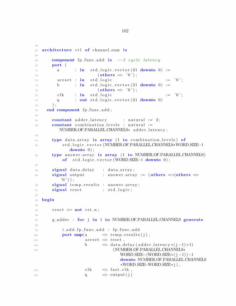
102
66
67 architecture r t l of channel sum i s68
69 component fp func add i s −−3 c y c l e l a t ency70 port (71 a : in s t d l o g i c v e c t o r (31 downto 0) :=72 ( others => ’ 0 ’ ) ;73 a r e s e t : in s t d l o g i c := ’ 0 ’ ;74 b : in s t d l o g i c v e c t o r (31 downto 0) :=75 ( others => ’ 0 ’ ) ;76 c l k : in s t d l o g i c := ’ 0 ’ ;77 q : out s t d l o g i c v e c t o r (31 downto 0)78 ) ;79 end component fp func add ;80
81 constant adde r l a t ency : natura l := 2 ;82 constant comb ina t i on l e v e l s : natura l :=
NUMBEROF PARALLEL CHANNELS∗ adde r l a t ency ;83
84 type data ar ray i s array (1 to comb ina t i on l e v e l s ) of85 s t d l o g i c v e c t o r (NUMBEROF PARALLEL CHANNELS∗WORD SIZE−1
downto 0) ;86 type answer array i s array (1 to NUMBEROF PARALLEL CHANNELS)
of s t d l o g i c v e c t o r (WORD SIZE−1 downto 0) ;87
88 signal data de lay : data ar ray ;89 signal output : answer array := ( others =>(others =>
’ 0 ’ ) ) ;90 signal t emp re su l t s : answer array ;91 signal r e s e t : s t d l o g i c ;92
93 begin94
95 r e s e t <= not r s t n ;96
97 g adder : for j in 1 to NUMBEROF PARALLEL CHANNELS generate98
99 i add fp func add : fp func add100 port map( a => t emp re su l t s ( j ) ,101 a r e s e t => r e s e t ,102 b => data de lay ( adder l a t ency ∗( j−1)+1)103 (NUMBEROF PARALLEL CHANNELS∗
WORD SIZE−(WORD SIZE∗( j−1) )−1downto NUMBEROF PARALLEL CHANNELS∗WORD SIZE−WORD SIZE∗ j ) ,
104 c l k => f a s t c l k ,105 q => output ( j )

103
106 ) ;107
108 end generate ;109
110 p i p e l i n e : process ( c lk , r s t n )111 begin112 i f ( r s t n = ’0 ’ ) then113 r e s u l t o u t <= ( others => ’ 0 ’ ) ;114 e l s i f ( r i s i n g e d g e ( c l k ) ) then115 for k in 1 to comb ina t i on l e v e l s loop116 i f ( k = 1) then117 data de lay (k ) <= data in ;118 else119 data de lay (k ) <= data de lay (k−1) ;120 end i f ;121 end loop ;122 for j in 1 to NUMBEROF PARALLEL CHANNELS loop123 i f ( j = 1) then124 t emp re su l t s ( j ) <= in t e r c e p t i n ;125 else126 t emp re su l t s ( j ) <= output ( j−1) ;127 end i f ;128 end loop ;129 r e s u l t o u t <= output (NUMBEROF PARALLEL CHANNELS) ;130 end i f ;131 end process ;132 end architecture ;
1 −−−−−−−−−−−−−−−−−−−−−−−−−−−−−−−−−−−−−−−−−−−−−−−−−−−−−−−−−−−−−2 −−3 −−! @ f i l e s o r t . vhd4 −−! @br ie f Sor t s p a r a l l e l i npu t s in descending order5 −−! @de t a i l s Sor t s input in two c l o c k c y c l e s and ou tpu t s6 −−! s o r t ed index numbers in add i t i on to so r t ed7 −−! r e s u l t s8 −−! @author Monica Whitaker9 −−! @date August 2016
10 −−! @copyright Copyright (C) 2016 Ross K. Snider and11 −−! Monica Whitaker12 −−13 −− This program i s f r e e so f tware : you can r e d i s t r i b u t e i t and/or14 −− modify i t under the terms o f the GNU General Pub l i c License15 −− as pub l i s h ed by the Free Sof tware Foundation , e i t h e r ve r s i on16 −− 3 o f the License , or ( at your opt ion ) any l a t e r ve r s i on .17 −−18 −− This program i s d i s t r i b u t e d in the hope t ha t i t w i l l be19 −− use fu l , but WITHOUT ANY WARRANTY; wi thout even the imp l i ed
104
20 −− warranty o f MERCHANTABILITY or FITNESS FOR A PARTICULAR21 −− PURPOSE. See the GNU General Pub l i c License f o r more d e t a i l s .22 −−23 −− You shou ld have r e c e i v ed a copy o f the GNU General Pub l i c24 −− License a long wi th t h i s program . I f not , see <h t t p ://www. gnu
. org / l i c e n s e s />.25 −−26 −− Monica Whitaker27 −− E l e c t r i c a l and Computer Engineer ing28 −− Montana S ta t e Un i v e r s i t y29 −− 610 Cob le i gh Ha l l30 −− Bozeman , MT 5971731 −− monica . whitaker@msu . montana . edu32 −−33 −−−−−−−−−−−−−−−−−−−−−−−−−−−−−−−−−−−−−−−−−−−−−−−−−−−−−−−−−−−−−34 l ibrary IEEE ; −−! Use standard l i b r a r y .35 use IEEE . STD LOGIC 1164 .ALL; −−! Use standard l o g i c e lements .36 use IEEE .NUMERIC STD.ALL; −−! Use numeric s tandard .37 use IEEE .MATHREAL.ALL; −−! Use r e a l math l i b r a r y38
39 use work . Sensor Package . a l l ; −−! Pro jec t cons tan t s packagef i l e
40 −−−−−−−−−−−−−−−−−−−−−−−−−−−−−−−−−−−−−−−−−−−−−−−−−−−−−−−−−−−−−41 −−42 −−! @br ie f s o r t43 −−! @de t a i l s Sor t s input in two c l o c k c y c l e s and ou tpu t s44 −−! s o r t ed index numbers in add i t i on to so r t ed45 −−! r e s u l t s46 −−! @param WORD SIZE Standard s i z e o f f l o a t i n g
po in t data47 −−! @param c l k Input c l k f o r data ra t e48 −−! @param r s t n Act ive low r e s e t49 −−! @param u l i s t i n Unsorted vec t o r o f va l u e s50 −−! @param s l i s t o u t Sorted vec t o r o f va l u e s51 −−! @param s l i s t i n d i c e s o u t Vector o f i n d i c e s o f s o r t ed
va l u e s in52 −−! s o r t ed order53 −−−−−−−−−−−−−−−−−−−−−−−−−−−−−−−−−−−−−−−−−−−−−−−−−−−−−−−−−−−−−54
55 entity s o r t i s56 generic (57 WORD SIZE : natura l := 3258 ) ;59 port (60 c l k : in s t d l o g i c ;61 r s t n : in s t d l o g i c ;
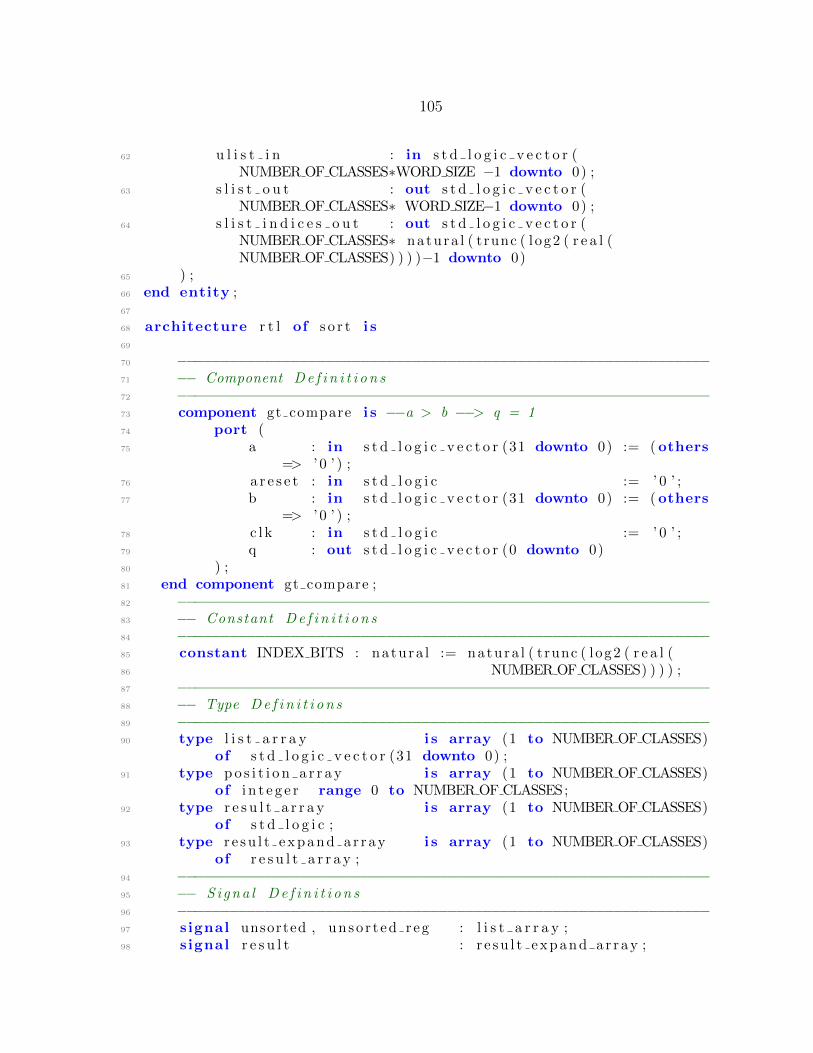
105
62 u l i s t i n : in s t d l o g i c v e c t o r (NUMBER OF CLASSES∗WORD SIZE −1 downto 0) ;
63 s l i s t o u t : out s t d l o g i c v e c t o r (NUMBER OF CLASSES∗ WORD SIZE−1 downto 0) ;
64 s l i s t i n d i c e s o u t : out s t d l o g i c v e c t o r (NUMBER OF CLASSES∗ natura l ( trunc ( log2 ( r e a l (NUMBER OF CLASSES) ) ) )−1 downto 0)
65 ) ;66 end entity ;67
68 architecture r t l of s o r t i s69
70 −−−−−−−−−−−−−−−−−−−−−−−−−−−−−−−−−−−−−−−−−−−−−−−−−−−−−−−−−−−−−71 −− Component De f i n i t i o n s72 −−−−−−−−−−−−−−−−−−−−−−−−−−−−−−−−−−−−−−−−−−−−−−−−−−−−−−−−−−−−−73 component gt compare i s −−a > b −−> q = 174 port (75 a : in s t d l o g i c v e c t o r (31 downto 0) := ( others
=> ’ 0 ’ ) ;76 a r e s e t : in s t d l o g i c := ’ 0 ’ ;77 b : in s t d l o g i c v e c t o r (31 downto 0) := ( others
=> ’ 0 ’ ) ;78 c l k : in s t d l o g i c := ’ 0 ’ ;79 q : out s t d l o g i c v e c t o r (0 downto 0)80 ) ;81 end component gt compare ;82 −−−−−−−−−−−−−−−−−−−−−−−−−−−−−−−−−−−−−−−−−−−−−−−−−−−−−−−−−−−−−83 −− Constant De f i n i t i o n s84 −−−−−−−−−−−−−−−−−−−−−−−−−−−−−−−−−−−−−−−−−−−−−−−−−−−−−−−−−−−−−85 constant INDEX BITS : natura l := natura l ( trunc ( log2 ( r e a l (86 NUMBER OF CLASSES) ) ) ) ;87 −−−−−−−−−−−−−−−−−−−−−−−−−−−−−−−−−−−−−−−−−−−−−−−−−−−−−−−−−−−−−88 −− Type De f i n i t i o n s89 −−−−−−−−−−−−−−−−−−−−−−−−−−−−−−−−−−−−−−−−−−−−−−−−−−−−−−−−−−−−−90 type l i s t a r r a y i s array (1 to NUMBER OF CLASSES)
of s t d l o g i c v e c t o r (31 downto 0) ;91 type po s i t i o n a r r a y i s array (1 to NUMBER OF CLASSES)
of i n t e g e r range 0 to NUMBER OF CLASSES;92 type r e s u l t a r r a y i s array (1 to NUMBER OF CLASSES)
of s t d l o g i c ;93 type r e su l t expand a r r ay i s array (1 to NUMBER OF CLASSES)
of r e s u l t a r r a y ;94 −−−−−−−−−−−−−−−−−−−−−−−−−−−−−−−−−−−−−−−−−−−−−−−−−−−−−−−−−−−−−95 −− S igna l De f i n i t i o n s96 −−−−−−−−−−−−−−−−−−−−−−−−−−−−−−−−−−−−−−−−−−−−−−−−−−−−−−−−−−−−−97 signal unsorted , unso r t ed reg : l i s t a r r a y ;98 signal r e s u l t : r e su l t expand a r r ay ;
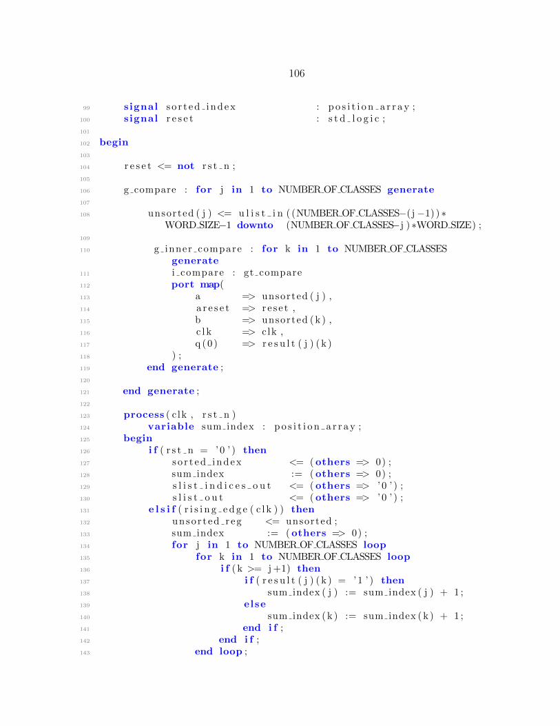
106
99 signal s o r t ed index : p o s i t i o n a r r a y ;100 signal r e s e t : s t d l o g i c ;101
102 begin103
104 r e s e t <= not r s t n ;105
106 g compare : for j in 1 to NUMBER OF CLASSES generate107
108 unsorted ( j ) <= u l i s t i n ( (NUMBER OF CLASSES−( j−1) ) ∗WORD SIZE−1 downto (NUMBER OF CLASSES−j ) ∗WORD SIZE) ;
109
110 g inner compare : for k in 1 to NUMBER OF CLASSESgenerate
111 i compare : gt compare112 port map(113 a => unsorted ( j ) ,114 a r e s e t => r e s e t ,115 b => unsorted (k ) ,116 c l k => c lk ,117 q (0 ) => r e s u l t ( j ) ( k )118 ) ;119 end generate ;120
121 end generate ;122
123 process ( c lk , r s t n )124 variable sum index : p o s i t i o n a r r a y ;125 begin126 i f ( r s t n = ’0 ’ ) then127 s o r t ed index <= ( others => 0) ;128 sum index := ( others => 0) ;129 s l i s t i n d i c e s o u t <= ( others => ’ 0 ’ ) ;130 s l i s t o u t <= ( others => ’ 0 ’ ) ;131 e l s i f ( r i s i n g e d g e ( c l k ) ) then132 unso r t ed reg <= unsorted ;133 sum index := ( others => 0) ;134 for j in 1 to NUMBER OF CLASSES loop135 for k in 1 to NUMBER OF CLASSES loop136 i f ( k >= j+1) then137 i f ( r e s u l t ( j ) ( k ) = ’1 ’ ) then138 sum index ( j ) := sum index ( j ) + 1 ;139 else140 sum index (k ) := sum index (k ) + 1 ;141 end i f ;142 end i f ;143 end loop ;

107
144 s o r t ed index ( j ) <= sum index ( j ) − 1 ; −−s t a r t from0
145 s l i s t i n d i c e s o u t (INDEX BITS∗(NUMBER OF CLASSES−146 ( s o r t ed index ( j ) ) )−1 downto INDEX BITS∗(147 NUMBER OF CLASSES−( s o r t ed index ( j )+1) ) ) <=148 s t d l o g i c v e c t o r ( to uns igned ( j , INDEX BITS) ) ;149 −−ordered l e a s t to g r e a t e s t150 s l i s t o u t (WORD SIZE∗(NUMBER OF CLASSES−
s o r t ed index ( j ) )−1151 downto WORD SIZE∗(NUMBER OF CLASSES−(
s o r t ed index ( j )+1) ) )152 <= unsor t ed reg ( j ) ;153 end loop ;154 end i f ;155 end process ;156 end architecture ;
1 −−−−−−−−−−−−−−−−−−−−−−−−−−−−−−−−−−−−−−−−−−−−−−−−−−−−−−−−−−−−−−−−−−−−−−−−−−−−
2 −−3 −−! @ f i l e o b j e c t t r a c k i n g . vhd4 −−! @br ie f Bui ld s up c l a s s i f i c a t i o n based on o b j e c t edges5 −−! @de t a i l s Uses input from hype r s p e c t r a l c l a s s i f i c a t i o n s and6 −−! monochrome edge d e t e c t i on to compi le o b j e c t7 −−! c l a s s i f i c a t i o n s over the i d e n t i f i e d p i x e l s .8 −−! @author Monica Whitaker9 −−! @date August 2016
10 −−! @copyright Copyright (C) 2016 Ross K. Snider and11 −−! Monica Whitaker12 −−13 −− This program i s f r e e so f tware : you can r e d i s t r i b u t e i t and/or14 −− modify i t under the terms o f the GNU General Pub l i c License15 −− as pub l i s h ed by the Free Sof tware Foundation , e i t h e r ve r s i on16 −− 3 o f the License , or ( at your opt ion ) any l a t e r ve r s i on .17 −−18 −− This program i s d i s t r i b u t e d in the hope t ha t i t w i l l be19 −− use fu l , but WITHOUT ANY WARRANTY; wi thout even the imp l i ed20 −− warranty o f MERCHANTABILITY or FITNESS FOR A PARTICULAR21 −− PURPOSE. See the GNU General Pub l i c License f o r more d e t a i l s .22 −−23 −− You shou ld have r e c e i v ed a copy o f the GNU General Pub l i c24 −− License a long wi th t h i s program . I f not , see <h t t p ://www. gnu
. org / l i c e n s e s />.25 −−26 −− Monica Whitaker27 −− E l e c t r i c a l and Computer Engineer ing

108
28 −− Montana S ta t e Un i v e r s i t y29 −− 610 Cob le i gh Ha l l30 −− Bozeman , MT 5971731 −− monica . whitaker@msu . montana . edu32 −−33 −−
−−−−−−−−−−−−−−−−−−−−−−−−−−−−−−−−−−−−−−−−−−−−−−−−−−−−−−−−−−−−−−−−−−−−−−−−−−
34 l ibrary IEEE ; −−! Use standard l i b r a r y .35 use IEEE . STD LOGIC 1164 .ALL ; −−! Use standard l o g i c e lements .36 use IEEE .NUMERIC STD.ALL ; −−! Use numeric s tandard .37 use IEEE .MATHREAL.ALL; −−! Use r e a l math l i b r a r y38
39 use work . Sensor Package . a l l ; −−! Pro jec t cons tan t s packagef i l e
40 −−−−−−−−−−−−−−−−−−−−−−−−−−−−−−−−−−−−−−−−−−−−−−−−−−−−−−−−−−−−−−−−−−−−−−−−−−−−
41 −−42 −−! @br ie f o b j e c t t r a c k i n g43 −−! @de t a i l s Uses input from hype r s p e c t r a l c l a s s i f i c a t i o n s and44 −−! monochrome edge d e t e c t i on to compi le o b j e c t45 −−! c l a s s i f i c a t i o n s over the i d e n t i f i e d p i x e l s .46 −−! Keeps array o f o b j e c t numbers based on p i x e l47 −−! number .48 −−! @param MAXOBJECTNUMBER Maximum number o f o b j e c t s49 −−! p o s s i b l e a t any one time50 −−! @param WORD SIZE Standard s i z e o f f l o a t i n g
po in t data51 −−! @param l i n e s c a n c l k Input c l k from transmiss ion
o f52 −−! monochrome data53 −−! @param da t a c l k Input c l o c k from
hype r s p e c t r a l54 −−! c l a s s i f i c a t i o n55 −−! @param f a s t c l k Input c l o c k running at t r i p l e56 −−! the speed o f the d a t a c l k57 −−! @param r s t n Act ive low r e s e t58 −−! @param l i n e r s t n Act ive low r e s e t f o r
l i n e s c a n c l k domain59 −−! @param l i n e s c an o b j Informat ion about o b j e c t60 −−! l o c a t i o n from l i n e s can camera61 −−! Contains l i n e number , o b j e c t62 −−! number , s t a r t p i x e l , end63 −−! p i x e l64 −−! @param new re su l t s Flag to i n d i c a t e new65 −−! h y p e r s p e c t r a l p i x e l r e s u l t s

109
66 −−! @param c l a s s r e s u l t s i n Hyper spec t ra l r e s u l t s v e c t o r67 −−! o f c l a s s p r o b a b i l i t i e s wi th68 −−! p i x e l number69 −−! @param de c i s i o n v e c t o r Vector o f o v e r a l l70 −−! p r o b a b i l i t i e s f o r c l a s s e s71 −−! and o b j e c t number .72 −−
−−−−−−−−−−−−−−−−−−−−−−−−−−−−−−−−−−−−−−−−−−−−−−−−−−−−−−−−−−−−−−−−−−−−−−−−−−
73 entity ob j e c t t r a c k i n g i s74 generic (MAXOBJECTNUMBER : natura l := 64 ;75 WORD SIZE : natura l := 3276 ) ;77 port ( l i n e s c a n c l k : in s t d l o g i c ;78 da ta c l k : in s t d l o g i c ;79 f a s t c l k : in s t d l o g i c ;80 r s t n : in s t d l o g i c ;81 l i n e r s t n : in s t d l o g i c ;82 l i n e s c a n ob j : in s t d l o g i c v e c t o r (
PIXEL ADDRESS SIZE∗2+OBJECT ADDRESS SIZE+WORD SIZE−1downto 0) ;
83 new re su l t s : in s t d l o g i c ;84 c l a s s r e s u l t s i n : in s t d l o g i c v e c t o r (
NUMBER OF CLASSES∗WORD SIZE+PIXEL ADDRESS SIZE−1downto 0) ;
85 d e c i s i o n v e c t o r : out s t d l o g i c v e c t o r (NUMBER OF CLASSES∗WORD SIZE+OBJECT ADDRESS SIZE−1downto 0)
86 ) ;87 end entity ;88
89 architecture arch of ob j e c t t r a c k i n g i s90
91 −−−−−−−−−−−−−−−−−−−−−−−−−−−−−−−−−−−−−−−−−−−−−−−−−−−−−−−−−−92 −− Component De f i n i t i o n s93 −−−−−−−−−−−−−−−−−−−−−−−−−−−−−−−−−−−−−−−−−−−−−−−−−−−−−−−−−−94 component memory block i s95 generic (96 num elements a : natura l ;97 num elements b : natura l ;98 s i z e a dd r e s s a : natura l ;99 s i z e a dd r e s s b : natura l ;
100 s i z e word a : natura l ;101 s i z e word b : natura l ;102 mem init : s t r i n g := "UNUSED"
103 ) ;104 port (

110
105 addre s s a : in s t d l o g i c v e c t o r ( s i z e add r e s s a −1downto 0) ;
106 addres s b : in s t d l o g i c v e c t o r ( s i z e add r e s s b −1downto 0) ;
107 c l o ck a : in s t d l o g i c := ’ 1 ’ ;108 c l o ck b : in s t d l o g i c := ’ 1 ’ ;109 data a : in s t d l o g i c v e c t o r ( s i z e word a−1
downto 0) ;110 data b : in s t d l o g i c v e c t o r ( s i ze word b−1
downto 0) ;111 wren a : in s t d l o g i c := ’ 0 ’ ;112 wren b : in s t d l o g i c := ’ 0 ’ ;113 q a : out s t d l o g i c v e c t o r ( s i z e word a−1
downto 0) ;114 q b : out s t d l o g i c v e c t o r ( s i ze word b−1
downto 0)115 ) ;116 end component memory block ;117
118 component fp func add i s −−3 c y c l e l a t ency119 port (120 a : in s t d l o g i c v e c t o r (31 downto 0) := ( others =>
’ 0 ’ ) ;121 a r e s e t : in s t d l o g i c := ’ 0 ’ ;122 b : in s t d l o g i c v e c t o r (31 downto 0) := ( others =>
’ 0 ’ ) ;123 c l k : in s t d l o g i c := ’ 0 ’ ;124 q : out s t d l o g i c v e c t o r (31 downto 0)125 ) ;126 end component fp func add ;127
128 −−−−−−−−−−−−−−−−−−−−−−−−−−−−−−−−−−−−−−−−−−−−−−−−−−−−−−−−−−129 −− Constant De f i n i t i o n s130 −−−−−−−−−−−−−−−−−−−−−−−−−−−−−−−−−−−−−−−−−−−−−−−−−−−−−−−−−−131 constant LINESCAN INPUT SIZE : natura l := WORD SIZE +
OBJECT ADDRESS SIZE + PIXEL ADDRESS SIZE∗2 ;132 −−Valid va l u e s = 1 ,2 ,4 ,8 ,16133 constant MEMORYRATIO : natura l := NUMBER OF CLASSES;134 constant CLASS NUMBER : natura l := natura l ( trunc ( log2 ( r e a l (
NUMBER OF CLASSES) ) ) ) ;135 constant ZEROS : s t d l o g i c v e c t o r (MEMORYRATIO∗WORD SIZE−1
downto 0) := ( others => ’ 0 ’ ) ;136
137 −−−−−−−−−−−−−−−−−−−−−−−−−−−−−−−−−−−−−−−−−−−−−−−−−−−−−−−−−−138 −− Type De f i n i t i o n s139 −−−−−−−−−−−−−−−−−−−−−−−−−−−−−−−−−−−−−−−−−−−−−−−−−−−−−−−−−−

111
140 type p i x e l a r r a y i s array (0 to NUMBER OF PIXELS) of i n t e g e rrange 0 to MAXOBJECTNUMBER;
141
142 −−−−−−−−−−−−−−−−−−−−−−−−−−−−−−−−−−−−−−−−−−−−−−−−−−−−−−−−−−143 −− S igna l De f i n i t i o n s144 −−−−−−−−−−−−−−−−−−−−−−−−−−−−−−−−−−−−−−−−−−−−−−−−−−−−−−−−−−145 signal p i x e l t r a c k e r , p r e v i o u s l i n e p i x e l s , p a s t l i n e :
p i x e l a r r a y ;146 signal r e s e t : s t d l o g i c ;147 signal f rame count : s t d l o g i c v e c t o r (WORD SIZE−1
downto 0) ;148 signal r e g r e s s l i n e : s t d l o g i c v e c t o r (WORD SIZE−1
downto 0) ;149 signal r eg reg , r e g l a t c h : s t d l o g i c v e c t o r (WORD SIZE−1
downto 0) ;150 signal p a s t l i n e s c a n l i n e : s t d l o g i c v e c t o r (WORD SIZE−1
downto 0) ;151
152 signal update mem address : s t d l o g i c v e c t o r (OBJECT ADDRESS SIZE−1 downto 0) ;
153 signal dec i s i on ve c to r t emp : s t d l o g i c v e c t o r (MEMORYRATIO∗WORD SIZE−1 downto 0) ;
154 signal mem write : s t d l o g i c ;155 signal o b j e c t c l e a r w r i t e : s t d l o g i c ;156 signal r eady wr i t e : s t d l o g i c ;157 signal r eady wr i t e2 : s t d l o g i c ;158 signal mem pixel : s t d l o g i c v e c t o r (
NUMBER OF CLASSES∗WORD SIZE−1 downto 0) ;159 signal combined pixe l : s t d l o g i c v e c t o r (
NUMBER OF CLASSES∗WORD SIZE−1 downto 0) ;160 signal new pix add : s t d l o g i c v e c t o r (
NUMBER OF CLASSES∗WORD SIZE−1 downto 0) ;161 signal new pixe l : s t d l o g i c v e c t o r (
NUMBER OF CLASSES∗WORD SIZE−1 downto 0) ;162
163 signal output mem address : s t d l o g i c v e c t o r (OBJECT ADDRESS SIZE−1 downto 0) ;
164 signal out object num : s t d l o g i c v e c t o r (OBJECT ADDRESS SIZE−1 downto 0) ;
165 signal newlinenum : s t d l o g i c v e c t o r (WORD SIZE−1downto 0) ;
166 signal p ix s t a r t , pixend : s t d l o g i c v e c t o r (PIXEL ADDRESS SIZE−1 downto 0) ;
167
168 signal object num : s t d l o g i c v e c t o r (OBJECT ADDRESS SIZE−1 downto 0) ;
169

112
170 signal s t a r t l i n e : s t d l o g i c ;171 signal r e g s t a r t l i n e : s t d l o g i c ;172 signal r e g s t a r t l i n e 2 : s t d l o g i c ;173
174 attribute noprune : boolean ;175 attribute noprune of p i x e l t r a c k e r : signal i s t rue ;176
177 begin178
179 ASSERT (MEMORYRATIO >= NUMBER OF CLASSES)180 report "Invalid number of classes for memory block"
181 severity e r r o r ;182
183 r e s e t <= not r s t n ;184
185 i c l a s s r e s u l t mem : memory block −−update on b , output on a186 generic map(187 num elements a => MAXOBJECTNUMBER,188 num elements b => MAXOBJECTNUMBER,189 s i z e a dd r e s s a => OBJECT ADDRESS SIZE,190 s i z e a dd r e s s b => OBJECT ADDRESS SIZE,191 s i z e word a => NUMBER OF CLASSES ∗ WORD SIZE,192 s i z e word b => NUMBER OF CLASSES ∗ WORD SIZE,193 mem init => "UNUSED"
194 )195 port map(196 addre s s a => output mem address ,197 addres s b => update mem address ,198 c l o ck a => data c lk ,199 c l o ck b => data c lk ,200 data a => ( others => ’ 0 ’ ) ,201 data b => combined pixe l ,202 wren a => ob j e c t c l e a r w r i t e ,203 wren b => mem write ,204 q a => dec i s i on vec to r t emp , −−r e g i s t e r e d205 q b => mem pixel206 ) ;207
208 accumulate : for k in 1 to NUMBER OF CLASSES generate209
210 i add fp func add : fp func add211 port map(212 a => mem pixel (WORD SIZE∗(NUMBER OF CLASSES−(k−1) )
−1 downto WORD SIZE∗(NUMBER OF CLASSES−k ) ) ,213 a r e s e t => r e s e t ,214 b => new pix add (WORD SIZE∗(NUMBER OF CLASSES−(k−1)
)−1 downto WORD SIZE∗(NUMBER OF CLASSES−k ) ) ,
113
215 c l k => f a s t c l k ,216 q => combined pixe l (WORD SIZE∗(NUMBER OF CLASSES−(k
−1) )−1 downto WORD SIZE∗(NUMBER OF CLASSES−k ) )217 ) ;218
219 end generate ;220
221
222 −−input from l i n e s can < l i n e#, o b j e c t#, s t a r t pix , end pix>223 a c c e p t p i x e l s : process ( l i n e s c an c l k , l i n e r s t n )224 variable c u r r e n t l i n e s c a n l i n e : s t d l o g i c v e c t o r (
WORD SIZE−1 downto 0) ;225 begin226 i f ( l i n e r s t n = ’0 ’ ) then227 p r e v i o u s l i n e p i x e l s <= ( others => 0) ;228 p i x e l t r a c k e r <= ( others => 0) ;229 r e g r e s s l i n e <= ( others => ’ 0 ’ ) ;230 p a s t l i n e s c a n l i n e <= ( others => ’ 0 ’ ) ;231 e l s i f ( r i s i n g e d g e ( l i n e s c a n c l k ) ) then232 −−l i n e coun t r e s e t = <zeros , ones , 0 ,NUMBER OF PIXELS−1>233 i f ( l i n e s c a n ob j (PIXEL ADDRESS SIZE−1 downto 0) =234 s t d l o g i c v e c t o r ( to uns igned (NUMBER OF PIXELS−1,235 PIXEL ADDRESS SIZE) ) and l i n e s c a n ob j (
PIXEL ADDRESS SIZE ∗236 2 − 1 downto PIXEL ADDRESS SIZE) =
s t d l o g i c v e c t o r (237 to uns igned (0 ,PIXEL ADDRESS SIZE) ) ) then238 s t a r t l i n e <= ’1 ’ ;239 else240 s t a r t l i n e <= ’0 ’ ;241 c u r r e n t l i n e s c a n l i n e := l i n e s c a n ob j (
LINESCAN INPUT SIZE−1 downtoLINESCAN INPUT SIZE−WORD SIZE) ;
242 object num <= l i n e s c a n ob j (LINESCAN INPUT SIZE−WORD SIZE−1 downto PIXEL ADDRESS SIZE∗2) ;
243 pixend <= l i n e s c a n ob j (PIXEL ADDRESS SIZE−1downto 0) ;
244 p i x s t a r t <= l i n e s c a n ob j (PIXEL ADDRESS SIZE∗2−1 downto PIXEL ADDRESS SIZE) ;
245 newlinenum <= l i n e s c a n ob j (LINESCAN INPUT SIZE−1downto LINESCAN INPUT SIZE−WORD SIZE) ;
246
247 i f ( unsigned ( c u r r e n t l i n e s c a n l i n e ) /=248 unsigned ( p a s t l i n e s c a n l i n e ) ) then249 −−new l i n e250 p r e v i o u s l i n e p i x e l s <= p i x e l t r a c k e r ;251 p i x e l t r a c k e r <= ( others => 0) ;

114
252 end i f ;253
254 for k in 1 to NUMBER OF PIXELS loop255 exit when k = unsigned ( pixend ) + 1 ;256 i f ( k >= unsigned ( p i x s t a r t ) and k <= unsigned (
pixend ) )257 then258 −−OBJECT NUMBER;259 p i x e l t r a c k e r ( k ) <= to i n t e g e r ( unsigned (
object num ) ) ;260 end i f ;261 end loop ;262 p a s t l i n e s c a n l i n e <= cu r r e n t l i n e s c a n l i n e ;263 r e g r e s s l i n e <= newlinenum ;264 end i f ;265 end i f ;266 end process ;267
268
269 −−one p i x e l r e s u l t a t a time , j u s t add in as needed !270 −−INPUT = <p ix#, c l a s s#, c l a s s r e s u l t>271 process ( data c lk , r s t n )272 variable pixel num : i n t e g e r range 0 to
NUMBER OF PIXELS−1;273 variable c u r r e n t l i n e : p i x e l a r r a y ;274 variable regress f rame num : s t d l o g i c v e c t o r (WORD SIZE
−1 downto 0) ;275 begin276 i f ( r s t n = ’0 ’ ) then277 new pixe l <= ( others => ’ 0 ’ ) ;278 regress f rame num := ( others => ’ 0 ’ ) ;279 update mem address <= ( others => ’ 0 ’ ) ;280 output mem address <= ( others => ’ 0 ’ ) ;281 r eady wr i t e <= ’0 ’ ;282 e l s i f ( r i s i n g e d g e ( da ta c l k ) ) then283 r e g s t a r t l i n e 2 <= s t a r t l i n e ;284 r e g s t a r t l i n e <= r e g s t a r t l i n e 2 ;285
286 r e g r e g <= r e g r e s s l i n e ;287 r e g l a t c h <= reg r e g ;288
289 i f ( r e g s t a r t l i n e = ’1 ’ ) then290 regress f rame num := ( others => ’ 0 ’ ) ;291 e l s i f ( n ew re su l t s = ’1 ’ ) then292 pixel num := t o i n t e g e r ( unsigned ( c l a s s r e s u l t s i n
(NUMBER OF CLASSES∗WORD SIZE+

115
PIXEL ADDRESS SIZE−1 downto NUMBER OF CLASSES∗WORD SIZE) ) ) ;
293 i f ( pixel num = 0) then294 regress f rame num := s t d l o g i c v e c t o r (
unsigned ( regress f rame num ) + 1) ;295 p a s t l i n e <= cu r r e n t l i n e ;296 i f ( unsigned ( regress f rame num ) = unsigned (
r e g l a t c h ) ) then297 c u r r e n t l i n e := p i x e l t r a c k e r ;298 else299 c u r r e n t l i n e := p r e v i o u s l i n e p i x e l s ;300 end i f ;301 end i f ;302 end i f ;303
304 i f ( n ew re su l t s = ’1 ’ ) then305 i f ( pixel num > 0 and pixel num < NUMBER OF PIXELS
−1) then306 i f ( c u r r e n t l i n e ( pixel num−1) /= 0 and307 c u r r e n t l i n e ( pixel num ) /= 0 and308 c u r r e n t l i n e ( pixel num+1) /= 0) then309 −−read from memory , add toge ther , re−
wr i t e to memory310 new pixe l <= c l a s s r e s u l t s i n (
NUMBER OF CLASSES∗311 WORD SIZE−1 downto 0) ;312
313 update mem address <= s t d l o g i c v e c t o r (to uns igned
314 ( c u r r e n t l i n e ( pixel num ) ,OBJECT ADDRESS SIZE) ) ;
315 r eady wr i t e <= ’1 ’ ;316 e l s i f ( c u r r e n t l i n e ( pixel num−1) = 0 and317 p a s t l i n e ( pixel num−1) /= 0) then318
319 i f ( c u r r e n t l i n e ( pixel num ) = 0 and320 p a s t l i n e ( pixel num ) /= 0) then321
322 output mem address <=s t d l o g i c v e c t o r (
323 to uns igned ( p a s t l i n e ( pixel num ) ,324 OBJECT ADDRESS SIZE) )
;325 end i f ;326 r eady wr i t e <= ’0 ’ ;327 new pixe l <= ( others => ’ 0 ’ ) ;328 else
116
329 r eady wr i t e <= ’0 ’ ;330 new pixe l <= ( others => ’ 0 ’ ) ;331 end i f ;332 else333 r eady wr i t e <= ’0 ’ ;334 new pixe l <= ( others => ’ 0 ’ ) ;335 end i f ;336 else337 new pixe l <= ( others => ’ 0 ’ ) ;338 r eady wr i t e <= ’0 ’ ;339
340 end i f ;341 new pix add <= new pixe l ;342 r eady wr i t e2 <= ready wr i t e ;−−p i p e l i n e wh i l e adder
opera t e s343 mem write <= ready wr i t e2 ;344 end i f ;345 end process ;346
347 output proc : process ( data c lk , r s t n )348 begin349 i f ( r s t n = ’0 ’ ) then350 d e c i s i o n v e c t o r <= ( others => ’ 0 ’ ) ;351 e l s i f ( r i s i n g e d g e ( da ta c l k ) ) then352 out object num <= output mem address ;353 i f ( d e c i s i on ve c to r t emp /= ZEROS) then354 d e c i s i o n v e c t o r <= out object num &
dec i s i on vec to r t emp ;355 o b j e c t c l e a r w r i t e <= ’1 ’ ;356 else357 d e c i s i o n v e c t o r <= ( others => ’ 0 ’ ) ;358 o b j e c t c l e a r w r i t e <= ’0 ’ ;359 end i f ;360 end i f ;361 end process ;362
363 end architecture ;
1 −−−−−−−−−−−−−−−−−−−−−−−−−−−−−−−−−−−−−−−−−−−−−−−−−−−−−−−−−−−−−2 −−3 −−! @ f i l e DRAM controller . vhd4 −−! @br ie f The master d r i v e r to p u l l data from DRAM.5 −−! @de t a i l s Passes bu r s t i n g reads from DRAM through b u f f e r6 −−! f o r use by system7 −−! @author Monica Whitaker8 −−! @date October 20159 −−! @copyright Copyright (C) 2015 Ross K. Snider and

117
10 −−! Monica Whitaker11 −−12 −− This program i s f r e e so f tware : you can r e d i s t r i b u t e i t and/or13 −− modify i t under the terms o f the GNU General Pub l i c License14 −− as pub l i s h ed by the Free Sof tware Foundation , e i t h e r ve r s i on15 −− 3 o f the License , or ( at your opt ion ) any l a t e r ve r s i on .16 −−17 −− This program i s d i s t r i b u t e d in the hope t ha t i t w i l l be18 −− use fu l , but WITHOUT ANY WARRANTY; wi thout even the imp l i ed19 −− warranty o f MERCHANTABILITY or FITNESS FOR A PARTICULAR20 −− PURPOSE. See the GNU General Pub l i c License f o r more d e t a i l s .21 −−22 −− You shou ld have r e c e i v ed a copy o f the GNU General Pub l i c23 −− License a long wi th t h i s program . I f not , see <h t t p ://www. gnu
. org / l i c e n s e s />.24 −−25 −− Monica Whitaker26 −− E l e c t r i c a l and Computer Engineer ing27 −− Montana S ta t e Un i v e r s i t y28 −− 610 Cob le i gh Ha l l29 −− Bozeman , MT 5971730 −− monica . whitaker@msu . montana . edu31 −−32 −−−−−−−−−−−−−−−−−−−−−−−−−−−−−−−−−−−−−−−−−−−−−−−−−−−−−−−−−−−−−33 l ibrary IEEE ;34 use IEEE . STD LOGIC 1164 .ALL;35 use i e e e . numer ic std . a l l ; −−! Use numeric s tandard36 use i e e e . math rea l . a l l ;37
38 use work . Sensor Package .ALL;39 −−−−−−−−−−−−−−−−−−−−−−−−−−−−−−−−−−−−−−−−−−−−−−−−−−−−−−−−−−−−−40 −−41 −−! @br ie f DRAM controller42 −−! @de t a i l s Passes bu r s t i n g reads from DRAM through b u f f e r43 −−! f o r use by system44 −−! @param memory clk Input r e f c l o c k
f o r DDR45 −−! @param sy s t em c l k Buf fer data
output c l o c k46 −−! @param r s t n Act ive low r e s e t47 −−! @param avm read master read Master Read
enab l e48 −−! @param avm read master address Master address49 −−! @param avm read master burs tcount Master bur s t coun t50 −−! @param avm read master readdata Master readdata51 −−! @param avm read mas ter readda tava l i d Master data v a l i d
118
52 −−! @param avm read mas ter wa i t reques t Master readwa i t r e que s t
53 −−! @param avm wr i t e mas te r wr i t e Master wr i t eenab l e
54 −−! @param avm wri te mas ter address Master wr i t eaddress
55 −−! @param avm wr i t e mas te r wr i t eda ta Master wr i t eda ta56 −−! @param avm wr i t e mas t e r wa i t r e que s t Master wr i t e
wa i t r e que s t57 −−! @param a v s c s r w r i t e S lave wr i t e
enab l e58 −−! @param av s c s r a dd r e s s S lave wr i t e
address59 −−! @param av s c s r w r i t e d a t a S lave wr i t eda ta60 −−! @param av s c s r wa i t r e q u e s t S lave wr i t e
wa i t r e que s t61 −−! @param w r i t e c l k Output o f
memory clk62 −−! @param r e a d s t a r t Enable read ing
from DDR63 −−! @param bu f f e r r e a d en Read enab l e f o r
FIFO64 −−! @param bu f f e r empty FIFO empty65 −−! @param bu f f e r r e a dda t a FIFO readdata66 −−67 −−−−−−−−−−−−−−−−−−−−−−−−−−−−−−−−−−−−−−−−−−−−−−−−−−−−−−−−−−−−−68 entity DRAM controller i s69 port ( memory clk : in s t d l o g i c ;70 sys t em c lk : in s t d l o g i c ;71 r s t n : in s t d l o g i c ;72
73 −−read master s i g n a l s74 avm read master read : out s t d l o g i c ;75 avm read master address : out s t d l o g i c v e c t o r (31
downto 0) ;76 avm read master burstcount : out s t d l o g i c v e c t o r (5
downto 0) ;77 avm read master readdata : in s t d l o g i c v e c t o r (127
downto 0) ;78 avm read master readdatava l id : in s t d l o g i c ;79 avm read master wai t request : in s t d l o g i c ;80
81 −−wr i t e master s i g n a l s −− debug wr i t i n g s i g n a l s82 avm wr i te master wr i t e : out s t d l o g i c ;83 avm wri te master address : out s t d l o g i c v e c t o r (31
downto 0) ;

119
84 avm wri te master wr i tedata : out s t d l o g i c v e c t o r (127downto 0) ;
85 avm wr i te maste r wa i t reques t : in s t d l o g i c ;86
87 −−expor t s i g n a l s f o r wr i t i n g88 a v s c s r w r i t e : in s t d l o g i c ;89 av s c s r add r e s s : in s t d l o g i c v e c t o r (31
downto 0) ;90 av s c s r w r i t e d a t a : in s t d l o g i c v e c t o r (127
downto 0) ;91 av s c s r wa i t r e qu e s t : out s t d l o g i c ;92 wr i t e c l k : out s t d l o g i c ;93
94 −−condui t expor t s i g n a l s95 r e a d s t a r t : in s t d l o g i c ; −− 1 i f wr i t e done96 bu f f e r r e ad en : in s t d l o g i c ;97 buf fer empty : out s t d l o g i c ;98 bu f f e r r e adda ta : out s t d l o g i c v e c t o r (127 downto
0)99 ) ;
100 end entity ;101
102 architecture c o n t r o l l e r a r c h of DRAM controller i s103 −−−−−−−−−−−−−−−−−−−−−−−−−−−−−−−−−−−−−−−−−−−−−−−−−−−−−−−−−−−−−104 −− Component De f i n i t i o n s105 −−−−−−−−−−−−−−−−−−−−−−−−−−−−−−−−−−−−−−−−−−−−−−−−−−−−−−−−−−−−−106 component d u a l c l o c k f i f o i s107 generic (108 lpm numwords : natura l ;109 lpm width : natura l ;110 lpm widthu : natura l ;111 rd sync de layp ipe : natura l ;112 under f l ow check ing : s t r i n g ;113 wrsync de layp ipe : natura l ) ;114 port (115 data : in s t d l o g i c v e c t o r ( lpm width − 1
downto 0)116 := ( others => ’X’ ) ;117 wrreq : in s t d l o g i c := ’X’ ;118 rdreq : in s t d l o g i c := ’X’ ;119 wrclk : in s t d l o g i c := ’X’ ;120 rdc lk : in s t d l o g i c := ’X’ ;121 a c l r : in s t d l o g i c := ’ 0 ’ ;122 q : out s t d l o g i c v e c t o r ( lpm width − 1
downto 0) ;123 rdempty : out s t d l o g i c ;124 wr f u l l : out s t d l o g i c ;

120
125 r d f u l l : out s t d l o g i c ;126 wrempty : out s t d l o g i c ;127 rdusedw : out s t d l o g i c v e c t o r ( lpm widthu − 1
downto 0) ;128 wrusedw : out s t d l o g i c v e c t o r ( lpm widthu − 1
downto 0) ;129 e c c s t a tu s : out s t d l o g i c v e c t o r (1 downto 0) ) ;130 end component d u a l c l o c k f i f o ;131 −−−−−−−−−−−−−−−−−−−−−−−−−−−−−−−−−−−−−−−−−−−−−−−−−−−−−−−−−−−−−132 −− Constant De f i n i t i o n s133 −−−−−−−−−−−−−−−−−−−−−−−−−−−−−−−−−−−−−−−−−−−−−−−−−−−−−−−−−−−−−134 constant BURST LENGTH : natura l := 32 ;135 constant BURST LENGTH SIZE : natura l := 6 ;136 constant BUFFERDEPTH : natura l := 1024 ;137 constant READDATA SIZE : natura l := DRAM DATA SIZE;138 constant TOTAL BURSTS : natura l := natura l ( trunc (
r e a l ( (NUMBER OF PIXELS∗NUMBER OF SPECTRAL BINS) /BURST LENGTH) ) ) ;
139 constant BYTES PERWORD : natura l := natura l ( trunc (r e a l (READDATA SIZE) / r e a l (8 ) ) ) ;
140 −−−−−−−−−−−−−−−−−−−−−−−−−−−−−−−−−−−−−−−−−−−−−−−−−−−−−−−−−−−−−141 −− Type De f i n i t i o n s142 −−−−−−−−−−−−−−−−−−−−−−−−−−−−−−−−−−−−−−−−−−−−−−−−−−−−−−−−−−−−−143 −− s t a t e machine s t a t e s144 type r e ad s t a t e s T i s ( i d l e ,145 f i f o w a i t ,146 mid burst ,147 f i n i s h r e a d s ) ;148 −−−−−−−−−−−−−−−−−−−−−−−−−−−−−−−−−−−−−−−−−−−−−−−−−−−−−−−−−−−−−149 −− S igna l Dec la ra t i ons150 −−−−−−−−−−−−−−−−−−−−−−−−−−−−−−−−−−−−−−−−−−−−−−−−−−−−−−−−−−−−−151 −− f i f o s i g n a l s152 signal bu f f e r w r i t e : s t d l o g i c ;153 signal b u f f e r f u l l : s t d l o g i c ;154 signal bu f f e r words : s t d l o g i c v e c t o r (9 downto 0) ;155
156 signal r e ad s t a t e : r e ad s t a t e s T ;157
158 −− ex t ra read master s i g n a l s159 −− the current read address160 signal r ead addre s s : s t d l o g i c v e c t o r (31 downto 0) ;161 −− t r a c k s the number o f b u r s t s completed162 signal burs t s comple ted : s t d l o g i c v e c t o r ( natura l ( trunc ( log2
( r e a l (TOTAL BURSTS) ) ) ) downto 0) ;163 −− t r a c k s the a v a i l a b l e room in the f i f o164 signal r o om i n f i f o : s t d l o g i c v e c t o r (10 downto 0) ;

121
165 −− t r a c k s the number o f t r an sa c t i on s t ha t are wa i t ing to bere turned
166 signal pending reads : s t d l o g i c v e c t o r (10 downto 0) ;167
168 −− ex t ra wr i t e master s i g n a l s169 −− the current wr i t e address170 signal wr i t e add r e s s : s t d l o g i c v e c t o r (31 downto 0) ;171 −− t r ack number o f va l u e s wr i t t en172 signal counter : i n t e g e r range 0 to TOTAL BURSTS∗
BURST LENGTH+1;173 −− DEBUG: a l e r t read FSM when wr i t i n g complete174 signal counter check : s t d l o g i c ;175 signal s t a r t add r e s s 1 : s t d l o g i c v e c t o r (31 downto 0) := x"
00000000" ;176
177 begin178 av s c s r wa i t r e qu e s t <= avm wr i te maste r wa i t reques t ;179 wr i t e c l k <= memory clk ;180 avm wri te master address <= av s c s r add r e s s ;181 avm wr i te master wr i te <= av s c s r w r i t e ;182 avm wri te master wr i tedata <= av s c s r w r i t e d a t a ;183
184 i d c f i f o b u f f e r : component d u a l c l o c k f i f o185 generic map(186 lpm numwords => BUFFER DEPTH,187 lpm width => DRAM DATA SIZE,188 lpm widthu => 10 ,189 rd sync de layp ipe => 4 ,190 under f l ow check ing => "OFF" ,191 wrsync de layp ipe => 4192 )193 port map(194 data => avm read master readdata ,195 wrreq => bu f f e r w r i t e ,196 rdreq => bu f f e r r e ad en ,197 wrclk => memory clk ,198 rdc lk => system clk ,199 q => bu f f e r r eaddata ,200 rdempty => buffer empty ,201 wr f u l l => b u f f e r f u l l ,202 a c l r => open ,203 e c c s t a tu s => open ,204 r d f u l l => open ,205 rdusedw => open ,206 wrempty => open ,207 wrusedw => bu f f e r words208 ) ;
122
209 −−−−−−−−−−−−−−−−−−−−−−−−−−−−−−−−−−−−−−−−−−−−−−−−−−−−−−−−−−−−−210 −−−−−−−−−−−−−−−−−−−−−−−−−−−−−−−−−−−−−−−−−−−−−−−−−−−−−−−−−−−−−211 −−READ FSM 1212 −− read l i g h t /dark matrix va l u e s −− addres se s x ”00000000” to
x”0FFFFFFF”213 −−−−−−−−−−−−−−−−−−−−−−−−−−−−−−−−−−−−−−−−−−−−−−−−−−−−−−−−−−−−−214 −−−−−−−−−−−−−−−−−−−−−−−−−−−−−−−−−−−−−−−−−−−−−−−−−−−−−−−−−−−−−215 read FSM 1 : process (memory clk , r s t n )216 begin217 i f ( r s t n = ’0 ’ or r e a d s t a r t = ’0 ’ ) then218 r e ad s t a t e <= i d l e ;219 r ead addre s s <= s t a r t add r e s s 1 ;220 burs t s comple ted <= ( others => ’ 0 ’ ) ;221 pending reads <= ( others => ’ 0 ’ ) ;222 e l s i f ( r i s i n g e d g e (memory clk ) ) then223
224 −− DEFAULT SECTION225 −− decrement the pending reads counter i f data i s re turned226 i f ( avm read master readdatava l id = ’1 ’ ) then227 pending reads <= s t d l o g i c v e c t o r ( unsigned ( pend ing reads )
− 1) ;228 end i f ;229
230 case r e ad s t a t e i s231 −− IDLE232 −− When i d l e j u s t s i t and wai t f o r the go f l a g .233 −− Only s t a r t i f the wr i t e s t a t e machine i s i d l e as i t
may234 −− be f i n i s h i n g a prev ious data t r an s f e r .235 −− S ta r t the machine by moving to the f i f o w a i t s t a t e and236 −− i n i t i a l i s i n g address and counters .237 when i d l e =>238 −− i f r e a d s t a r t = ’1 ’ then239 r e ad s t a t e <= f i f o w a i t ;240 r ead addre s s <= s t a r t add r e s s 1 ;241 pending reads <= ( others => ’ 0 ’ ) ;242 burs t s comple ted <= ( others => ’ 0 ’ ) ;243 −−end i f ;244
245 −− FIFO WAIT246 −− When in t h i s s t a t e wai t f o r the f i f o to have
s u f f i c i e n t247 −− space f o r a complete bu r s t . I f so , s t a r t a
bu r s t by248 −− moving to the mid burs t s t a t e . When moving to
mid bu r s t

123
249 −− add the bu r s t va lue to the pending readscounter .
250 when f i f o w a i t =>251 −− check t ha t f i f o has enough space f o r 32 word bu r s t252 i f ( unsigned ( r o om i n f i f o ) >= BURST LENGTH + 5) then253 r e ad s t a t e <= mid burst ;254 −− add 32 to the pending reads counter but be255 −− mindfu l t h a t a word may be re turned at
the same256 −− t ime257 i f ( avm read master readdatava l id = ’0 ’ ) then258 pending reads <= s t d l o g i c v e c t o r ( unsigned (
pend ing reads ) + BURST LENGTH) ;259 else260 pending reads <= s t d l o g i c v e c t o r ( unsigned (
pend ing reads ) + BURST LENGTH−1) ;261 end i f ;262
263 end i f ;264
265 −− MID BURST266 −− Count bu r s t s267 −− I f a l l b u r s t s complete go to f i n i s h r e a d s s t a t e .268 −− Otherwise s tay in t h i s s t a t e i f t h e r e i s room in f i f o
or269 −− re turn to f i f o w a i t i f not . As each bu r s t i s
completed270 −− increment address , b u r s t s completed counter
and pending271 −− reads counter . Be mindfu l to do noth ing i f
wa i t r e que s t272 −− i s a c t i v e273 when mid burst =>274 −− i f wa i t r e que s t i s a c t i v e do nothing , o the rw i s e . . .275 i f ( avm read master wai t request /= ’1 ’ ) then276 i f ( burs t s comple ted = s t d l o g i c v e c t o r ( to uns igned (
TOTAL BURSTS − 1 , natura l ( trunc ( log2 ( r e a l (TOTAL BURSTS) ) ) )+1) ) ) then
277 r e ad s t a t e <= f i n i s h r e a d s ;278 −− no need to check f o r pending reads complete279 −− as we ’ ve j u s t r e que s t ed another 32
words280 else281 burs t s comple ted <= s t d l o g i c v e c t o r ( unsigned (
burs t s comple ted ) + 1) ;282 r ead addre s s <= s t d l o g i c v e c t o r ( unsigned (
r ead addre s s ) + BURST LENGTH∗BYTES PERWORD) ;

124
283 i f ( unsigned ( r o om i n f i f o ) >= BURST LENGTH + 5)284 then285 r e ad s t a t e <= mid burst ;286 −− add 32 to the pending reads counter but287 −− be mindfu l t h a t a word may be
re turned288 −− at the same time289 i f ( avm read master readdatava l id = ’0 ’ ) then290 pending reads <= s t d l o g i c v e c t o r ( unsigned (
pend ing reads ) + BURST LENGTH) ;291 else292 pending reads <= s t d l o g i c v e c t o r ( unsigned (
pend ing reads ) + BURST LENGTH − 1) ;293 end i f ;294 else295 r e ad s t a t e <= f i f o w a i t ;296 end i f ;297 end i f ;298
299 end i f ;300
301 −− FINISH READS302 −− Al l the read address phases are complete but t h e r e
w i l l303 −− be readdata pending . Jus t s i t and wai t u n t i l
t h e r e i s no304 −− readdata pending and then move to i d l e s t a t e .
Note t ha t305 −− the pend ing reads counter i s decremented in
the d e f a u l t306 −− s e c t i on above .307 when f i n i s h r e a d s =>308 i f ( avm read master readdatava l id = ’1 ’ ) then309 i f ( unsigned ( pend ing reads ) = 1) then310 r e ad s t a t e <= i d l e ;311 end i f ;312 end i f ;313
314 end case ;315 end i f ;316 end process ;317
318 avm read master read <= ’1 ’ when r e ad s t a t e = mid burst else’ 0 ’ ;
319
125
320 r o om i n f i f o <= s t d l o g i c v e c t o r ( r e s i z e ( ( to uns igned (BUFFER DEPTH, natura l ( trunc ( log2 ( r e a l (BUFFERDEPTH) ) ) ) + 1)− unsigned ( bu f f e r words ) − unsigned ( pend ing reads ) ) , 11) ) ;
321
322 avm read master address <= read addre s s ;323
324 −− s imply wr i t e data in t o the f i f o as i t comes in ( reada s s e r t e d and
325 −− wa i t r e que s t not a c t i v e )326 bu f f e r w r i t e <= avm read master readdatava l id ;327
328 avm read master burstcount <= s t d l o g i c v e c t o r ( to uns igned (BURST LENGTH, BURST LENGTH SIZE) ) ;
329
330 −−−−−−−−−−−−−−−−−−−−−−−−−−−−−−−−−−−−−−−−−−−−−−−−−−−−−−−−−−−−−331 −− DEBUG sec t i on332 −−−−−−−−−−−−−−−−−−−−−−−−−−−−−−−−−−−−−−−−−−−−−−−−−−−−−−−−−−−−−333 −− −− Writes counter va l u e s f o r t e s t i n g purposes .334 −− write FSM : process (memory clk , r s t n )335 −− beg in336 −− i f ( r s t n = ’0 ’ ) then337 −−wr i t e add r e s s <= s t a r t a d d r e s s 1 ;338 −−counter check <= ’0 ’ ;339 −−counter <= 0;340 −−avm wr i t e mas te r wr i t e <= ’1 ’ ;341 −− e l s i f ( r i s i n g e d g e (memory clk ) ) then342 −− i f ( avm wr i t e mas t e r wa i t r e que s t /= ’1 ’ ) then343
344
345 −− i f ( counter = TOTAL BURSTS∗BURST LENGTH+1) then346 −− avm wr i t e mas te r wr i t e <= ’0 ’ ;347 −− counter check <= ’1 ’ ;348 −− e l s e349 −− avm wr i t e mas t e r wr i t eda ta <=
s t d l o g i c v e c t o r (350 −− t o uns i gned ( counter ,
READDATA SIZE) ) ;351 −− counter <= counter + 1;352 −− wr i t e add r e s s <= s t d l o g i c v e c t o r ( unsigned
(353 −− wr i t e add r e s s ) +
BYTES PERWORD) ;354 −− end i f ;355 −− end i f ;356 −− end i f ;357 −− end process ;358

126
359 −− a v s c s r wa i t r e q u e s t <= avm wr i t e mas t e r wa i t r e que s t ;360
361 end architecture ;
1 −−−−−−−−−−−−−−−−−−−−−−−−−−−−−−−−−−−−−−−−−−−−−−−−−−−−−−−−−−−−−−2 −−3 −−! @ f i l e x c v r co r e . vhd4 −−! @br ie f Transmission i n t e r f a c e5 −−! @de t a i l s Contains t r an s c e i v e r phy and s e r i a l l i t e core f o r6 −−! t ransmiss ion over t r an s c e i v e r s7 −−! @author Monica Whitaker8 −−! @date August 20169 −−! @copyright Copyright (C) 2016 Ross K. Snider and
10 −−! Monica Whitaker11 −−12 −− This program i s f r e e so f tware : you can r e d i s t r i b u t e i t and/or13 −− modify i t under the terms o f the GNU General Pub l i c License14 −− as pub l i s h ed by the Free Sof tware Foundation , e i t h e r ve r s i on15 −− 3 o f the License , or ( at your opt ion ) any l a t e r ve r s i on .16 −−17 −− This program i s d i s t r i b u t e d in the hope t ha t i t w i l l be18 −− use fu l , but WITHOUT ANY WARRANTY; wi thout even the imp l i ed19 −− warranty o f MERCHANTABILITY or FITNESS FOR A PARTICULAR20 −− PURPOSE. See the GNU General Pub l i c License f o r more d e t a i l s .21 −−22 −− You shou ld have r e c e i v ed a copy o f the GNU General Pub l i c23 −− License a long wi th t h i s program . I f not , see <h t t p ://www. gnu
. org / l i c e n s e s />.24 −−25 −− Monica Whitaker26 −− E l e c t r i c a l and Computer Engineer ing27 −− Montana S ta t e Un i v e r s i t y28 −− 610 Cob le i gh Ha l l29 −− Bozeman , MT 5971730 −− monica . whitaker@msu . montana . edu31 −−32 −−−−−−−−−−−−−−−−−−−−−−−−−−−−−−−−−−−−−−−−−−−−−−−−−−−−−−−−−−−−−−−33 l ibrary IEEE ; −−! Use standard l i b r a r y .34 use IEEE . STD LOGIC 1164 .ALL; −−! Use standard l o g i c e lements .35 −−−−−−−−−−−−−−−−−−−−−−−−−−−−−−−−−−−−−−−−−−−−−−−−−−−−−−−−−−−−−−−−36 −−37 −−! @br ie f xcvr core38 −−! @de t a i l s Contains t r an s c e i v e r phy and s e r i a l l i t e core f o r39 −−! t ransmiss ion over t r an s c e i v e r s40 −−! @param clk 100MHz Input c l k f o r phy
management

127
41 −−! @param x c v r r e f c l k Transce iver p l l r e f e r encec l o c k
42 −−! @param c l k da t a Clock f o r A t l an t i ci n t e r f a c e
43 −−! @param r e s e t Act ive h igh r e s e t44 −−! @param re s e t n Act ive low r e s e t45 −−! @param r x s e r i a l d a t a S e r i a l r e c e i v e r i n t e r f a c e46 −−! @param t x s e r i a l d a t a S e r i a l t ransmiss ion
i n t e r f a c e47 −−! @param tx r eady Ready s i g n a l f o r
t ransmiss ion48 −−! @param rx ready Ready s i g n a l f o r r e c e i v e r49 −−! @param s t a t r r l i n k Ind i c a t e s l i n k i s up50 −−! @param tda t Data to t ransmi t51 −−! @param tdav Data a v a i l a b l e52 −−! @param tena Enable t ransmiss ion53 −−! @param tsop Transmit s t a r t o f packe t54 −−! @param teop Transmit end o f packe t55 −−! @param t e r r Error in t ransmi t data56 −−! @param tmty Number o f empty by t e s in57 −−! t ransmi t data58 −−! @param taddr Address o f packe t to send59 −−! @param rdav Data a v a i l a b l e60 −−! @param r va l Data v a l i d61 −−! @param rdat Incoming data62 −−! @param rsop Receiver s t a r t o f packe t
s i g n a l63 −−! @param reop Receiver end o f packe t
s i g n a l64 −−! @param rer r Receive error65 −−! @param rmty Number o f empty b y t e s in66 −−! r e c e i v ed data67 −−! @param raddr Address o f packe t
r e c e i v ed68 −−! @param e r r r r c r c CRC error found69 −−! @param r e c o n f i g r e s e t Reset f o r r e c on f i g u r a t i on
i n t e r f a c e70 −−! @param re con f i g r e ad Read r e que s t71 −−! @param r e c on f i g w r i t e Write r e que s t72 −−! @param re con f i g a dd r e s s Recon f i gura t ion address73 −−! @param r e c on f i g w r i t e d a t a Data to wr i t e on74 −−! r e c on f i g u r a t i on i n t e r f a c e75 −−! @param r e c on f i g wa i t r e q u e s t Waitrequest from76 −−! r e c on f i g u r a t i on i n t e r f a c e77 −−! @param recon f i g r e adda t a Data read from78 −−! r e c on f i g u r a t i on i n t e r f a c e79 −−−−−−−−−−−−−−−−−−−−−−−−−−−−−−−−−−−−−−−−−−−−−−−−−−−−−−−−−−−−−

128
80 entity xcv r co r e i s81 generic (82 NUMBER OF LANES : natura l := 1 ;83 LANEWIDTH : natura l := 3284 ) ;85 port (86 clk 50MHz : in s t d l o g i c ;87 x c v r r e f c l k : in s t d l o g i c ;88 c lkdata : in s t d l o g i c ;89 r e s e t : in s t d l o g i c ;90 r e s e t n : in s t d l o g i c ;91 r x s e r i a l d a t a : in s t d l o g i c ;92 t x s e r i a l d a t a : out s t d l o g i c ;93
94 tx ready : out s t d l o g i c ;95 rx ready : out s t d l o g i c ;96
97 s t a t r r l i n k : out s t d l o g i c ;98
99 tdat : in s t d l o g i c v e c t o r ( ( (NUMBER OF LANES ∗ LANEWIDTH)−1) downto 0) ;
100 tdav : out s t d l o g i c ;101 tena : in s t d l o g i c ;102 tsop : in s t d l o g i c ;103 teop : in s t d l o g i c ;104 t e r r : in s t d l o g i c ;105 tmty : in s t d l o g i c v e c t o r (1 downto 0)
;106 taddr : in s t d l o g i c v e c t o r (7 downto 0)
;107
108 rdat : out s t d l o g i c v e c t o r ( ( (NUMBER OF LANES ∗ LANEWIDTH)−1) downto 0) ;
109 rdav : out s t d l o g i c ;110 r va l : out s t d l o g i c ;111 rena : in s t d l o g i c ;112 rsop : out s t d l o g i c ;113 reop : out s t d l o g i c ;114 r e r r : out s t d l o g i c ;115 rmty : out s t d l o g i c v e c t o r (1 downto
0) ;116 raddr : out s t d l o g i c v e c t o r (7 downto
0) ;117
118 e r r c r c l o c k : out s t d l o g i c ;119
120 r e c o n f i g r e s e t : in s t d l o g i c ;

129
121 r e c on f i g r e ad : in s t d l o g i c ;122 r e c o n f i g w r i t e : in s t d l o g i c ;123 r e c on f i g add r e s s : in s t d l o g i c v e c t o r (9 downto 0)
;124 r e c on f i g w r i t e d a t a : in s t d l o g i c v e c t o r (31 downto
0) ;125 r e c on f i g wa i t r e qu e s t : out s t d l o g i c ;126 r e c on f i g r e adda t a : out s t d l o g i c v e c t o r (31 downto
0)127 ) ;128 end entity ;129
130 architecture arch of xcv r co r e i s131 −−−−−−−−−−−−−−−−−−−−−−−−−−−−−−−−−−−−−−−−−−−−−−−−−−−−−−−−−−−−−132 −− Component De f i n i t i o n s133 −−−−−−−−−−−−−−−−−−−−−−−−−−−−−−−−−−−−−−−−−−−−−−−−−−−−−−−−−−−−−134 component a10 xcvr phy i s135 port (136 r x ana l o g r e s e t : in s t d l o g i c v e c t o r (0
downto 0) := ( others => ’ 0 ’ ) ;137 r x ca l bu sy : out s t d l o g i c v e c t o r (0
downto 0) ;138 r x c d r r e f c l k 0 : in s t d l o g i c := ’ 0 ’ ;139 r x c l k ou t : out s t d l o g i c v e c t o r (0
downto 0) ;140 r x c o r e c l k i n : in s t d l o g i c v e c t o r (0
downto 0) := ( others => ’ 0 ’ ) ;141 rx datak : out s t d l o g i c v e c t o r (3
downto 0) ;142 r x d i g i t a l r e s e t : in s t d l o g i c v e c t o r (0
downto 0) := ( others => ’ 0 ’ ) ;143 r x d i s p e r r : out s t d l o g i c v e c t o r (3
downto 0) ;144 r x e r r d e t e c t : out s t d l o g i c v e c t o r (3
downto 0) ;145 r x i s l o c k e d t od a t a : out s t d l o g i c v e c t o r (0
downto 0) ;146 r x i s l o c k e d t o r e f : out s t d l o g i c v e c t o r (0
downto 0) ;147 r x p a r a l l e l d a t a : out s t d l o g i c v e c t o r (31
downto 0) ;148 r x pa t t e rnde t e c t : out s t d l o g i c v e c t o r (3
downto 0) ;149 rx runn ingd i sp : out s t d l o g i c v e c t o r (3
downto 0) ;150 r x s e r i a l d a t a : in s t d l o g i c v e c t o r (0
downto 0) := ( others => ’ 0 ’ ) ;

130
151 r x sync s t a tu s : out s t d l o g i c v e c t o r (3downto 0) ;
152 t x ana l o g r e s e t : in s t d l o g i c v e c t o r (0downto 0) := ( others => ’ 0 ’ ) ;
153 t x ca l bu sy : out s t d l o g i c v e c t o r (0downto 0) ;
154 t x c l k ou t : out s t d l o g i c v e c t o r (0downto 0) ;
155 t x c o r e c l k i n : in s t d l o g i c v e c t o r (0downto 0) := ( others => ’ 0 ’ ) ;
156 tx datak : in s t d l o g i c v e c t o r (3downto 0) := ( others => ’ 0 ’ ) ;
157 t x d i g i t a l r e s e t : in s t d l o g i c v e c t o r (0downto 0) := ( others => ’ 0 ’ ) ;
158 t x p a r a l l e l d a t a : in s t d l o g i c v e c t o r (31downto 0) := ( others => ’ 0 ’ ) ;
159 t x s e r i a l c l k 0 : in s t d l o g i c v e c t o r (0downto 0) := ( others => ’ 0 ’ ) ;
160 t x s e r i a l d a t a : out s t d l o g i c v e c t o r (0downto 0) ;
161 unu s ed r x pa r a l l e l d a t a : out s t d l o g i c v e c t o r (71downto 0) ;
162 unu s ed t x pa r a l l e l d a t a : in s t d l o g i c v e c t o r (91downto 0) := ( others => ’ 0 ’ )
163 ) ;164 end component a10 xcvr phy ;165
166 component s l 2 c o r e IS167 port (168 r x p a r a l l e l d a t a o u t : in s t d l o g i c v e c t o r (31
downto 0) ;169 r x c o r e c l k : in s t d l o g i c ;170 r x c t r l d e t e c t : in s t d l o g i c v e c t o r (3
downto 0) ;171 s t a t r r p a t t d e t : in s t d l o g i c v e c t o r (3
downto 0) ;172 e r r r r d i s p : in s t d l o g i c v e c t o r (3
downto 0) ;173 t x c o r e c l k : in s t d l o g i c ;174 c t r l t c f o r c e t r a i n : in s t d l o g i c ;175 mreset n : in s t d l o g i c ;176 rx rdp c l k : in s t d l o g i c ;177 rxrdp ena : in s t d l o g i c ;178 −− r e c e i v e FIFO th r e s ho l d low − un i t s in e lements179 c t l r x r d p f t l : in s t d l o g i c v e c t o r (7
downto 0) ;180 c t l rx rdp eopdav : in s t d l o g i c ;
131
181 tx rdp c l k : in s t d l o g i c ;182 txrdp ena : in s t d l o g i c ;183 txrdp sop : in s t d l o g i c ;184 txrdp eop : in s t d l o g i c ;185 t x rdp e r r : in s t d l o g i c ;186 txrdp mty : in s t d l o g i c v e c t o r (1
downto 0) ;187 txrdp dat : in s t d l o g i c v e c t o r (31
downto 0) ;188 txrdp adr : in s t d l o g i c v e c t o r (7
downto 0) ;189 −− t ransmi t FIFO bu f f e r t h r e s h o l d h igh190 c t l t x r d p f t h : in s t d l o g i c v e c t o r (7
downto 0) ;191 f l i p p o l a r i t y : out s t d l o g i c ;192 r r e f c l k : out s t d l o g i c ;193 s t a t r r l i n k : out s t d l o g i c ;194 e r r r r 8 b e r r d e t : in s t d l o g i c v e c t o r (3
downto 0) ;195 t x p a r a l l e l d a t a i n : out s t d l o g i c v e c t o r (31
downto 0) ;196 t x c t r l e n a b l e : out s t d l o g i c v e c t o r (3
downto 0) ;197 t x c o r e c l o c k : out s t d l o g i c ;198 rxrdp sop : out s t d l o g i c ;199 rxrdp eop : out s t d l o g i c ;200 r x rdp e r r : out s t d l o g i c ;201 rxrdp mty : out s t d l o g i c v e c t o r (1
downto 0) ;202 rxrdp dat : out s t d l o g i c v e c t o r (31
downto 0) ;203 rxrdp adr : out s t d l o g i c v e c t o r (7
downto 0) ;204 rx rdp va l : out s t d l o g i c ;205 rxrdp dav : out s t d l o g i c ;206 −− At l an t i c FIFO bu f f e r i s empty207 s tat rxrdp empty : out s t d l o g i c ;208 −− At l an t i c FIFO bu f f e r ove r f l ow and data l o s t209 e r r t c r x r dp o f lw : out s t d l o g i c ;210 −− At l an t i c FIFO bu f f e r ove r f l ow and data l o s t211 e r r t x r dp o f lw : out s t d l o g i c ;212 txrdp dav : out s t d l o g i c ;213 −− f r equency o f f s e t t o l e r anc e FIFO bu f f e r ove r f l ow214 −− l i n k r e s t a r t s215 e r r r r f o f f r e o f l w : out s t d l o g i c ;216 −− f r equency o f f s e t t o l e r anc e FIFO bu f f e r under f low217 s t a t t c f o f f r e emp t y : out s t d l o g i c ;

132
218 −− end o f bad packe t charac t e r r e c e i v ed219 s t a t r r e bp r x : out s t d l o g i c ;220 −− BIP−8 error d e t e c t e d in l i n k management packe t221 e r r r r b i p 8 : out s t d l o g i c ;222 −− CRC error de t e c t e d223 e r r r r c r c : out s t d l o g i c ;224 e r r r r f c r x b n e : out s t d l o g i c ;225 e r r r r r o e r x bn e : out s t d l o g i c ;226 −− i n v a l i d l i n k management packe t r e c e i v ed227 e r r r r i n v a l i d lmp r x : out s t d l o g i c ;228 −− s t a r t o f data con t r o l word miss ing229 e r r r r m i s s i n g s t a r t d cw : out s t d l o g i c ;230 −− s t a r t and end address f i e l d s do not match231 e r r r r addr mismatch : out s t d l o g i c ;232 −− p o s s i b l e c a t a s t r o ph i c error233 e r r r r p o l r e v r e q u i r e d : out s t d l o g i c234 ) ;235 end component ;236
237 component d u a l c l o c k f i f o i s238 generic (239 enab l e e c c : s t r i n g := "FALSE" ;240 i n t ended dev i c e f am i l y : s t r i n g := "Arria 10" ;241 lpm hint : s t r i n g242 := "
DISABLE_DCFIFO_EMBEDDED_TIMING_CONSTRAINT
=TRUE" ;243 lpm numwords : natura l ;244 lpm showahead : s t r i n g := "OFF" ;245 lpm type : s t r i n g := "dcfifo" ;246 lpm width : natura l ;247 lpm widthu : natura l ;248 ove r f l ow check ing : s t r i n g := "ON" ;249 rd sync de layp ipe : natura l ;250 under f l ow check ing : s t r i n g := "ON" ;251 use eab : s t r i n g := "ON" ;252 wrsync de layp ipe : natura l253 ) ;254 port (255 data : in s t d l o g i c v e c t o r ( lpm width − 1
downto 0) := ( others => ’X’ ) ;256 wrreq : in s t d l o g i c := ’X’ ;257 rdreq : in s t d l o g i c := ’X’ ;258 wrclk : in s t d l o g i c := ’X’ ;259 rdc lk : in s t d l o g i c := ’X’ ;260 a c l r : in s t d l o g i c := ’ 0 ’ ;
133
261 q : out s t d l o g i c v e c t o r ( lpm width − 1downto 0) ;
262 rdempty : out s t d l o g i c ;263 wr f u l l : out s t d l o g i c ;264 r d f u l l : out s t d l o g i c ;265 wrempty : out s t d l o g i c ;266 rdusedw : out s t d l o g i c v e c t o r ( lpm widthu − 1
downto 0) ;267 wrusedw : out s t d l o g i c v e c t o r ( lpm widthu − 1
downto 0) ;268 e c c s t a tu s : out s t d l o g i c v e c t o r (1 downto 0)269 ) ;270 end component ;271
272 component x c v r p l l i s273 port (274 p l l c a l b u s y : out s t d l o g i c ;275 p l l l o c k e d : out s t d l o g i c ;276 pll powerdown : in s t d l o g i c := ’ 0 ’ ;277 p l l r e f c l k 0 : in s t d l o g i c := ’ 0 ’ ;278 t x s e r i a l c l k : out s t d l o g i c279 ) ;280 end component ;281
282 component x c v r r e s e t i s283 port (284 c l o ck : in s t d l o g i c := ’ 0 ’ ;285 p l l l o c k e d : in s t d l o g i c v e c t o r (0 downto 0)
:= ( others => ’ 0 ’ ) ;286 pll powerdown : out s t d l o g i c v e c t o r (0 downto 0)
;287 p l l s e l e c t : in s t d l o g i c v e c t o r (0 downto 0)
:= ( others => ’ 0 ’ ) ;288 r e s e t : in s t d l o g i c := ’ 0 ’ ;289 r x ana l o g r e s e t : out s t d l o g i c v e c t o r (0 downto 0)
;290 r x ca l bu sy : in s t d l o g i c v e c t o r (0 downto 0)
:= ( others => ’ 0 ’ ) ;291 r x d i g i t a l r e s e t : out s t d l o g i c v e c t o r (0 downto 0)
;292 r x i s l o c k e d t od a t a : in s t d l o g i c v e c t o r (0 downto 0)
:= ( others => ’ 0 ’ ) ;293 rx ready : out s t d l o g i c v e c t o r (0 downto 0)
;294 t x ana l o g r e s e t : out s t d l o g i c v e c t o r (0 downto 0)
;

134
295 t x ca l bu sy : in s t d l o g i c v e c t o r (0 downto 0):= ( others => ’ 0 ’ ) ;
296 t x d i g i t a l r e s e t : out s t d l o g i c v e c t o r (0 downto 0);
297 tx ready : out s t d l o g i c v e c t o r (0 downto 0)298 ) ;299 end component ;300
301 −−−−−−−−−−−−−−−−−−−−−−−−−−−−−−−−−−−−−−−−−−−−−−−−−−−−−−−−−−−−−302 −− S igna l De f i n i t i o n s303 −−−−−−−−−−−−−−−−−−−−−−−−−−−−−−−−−−−−−−−−−−−−−−−−−−−−−−−−−−−−−304 signal ONES : s t d l o g i c v e c t o r (
NUMBER OF LANES−1 downto 0) ;305
306 signal r x f r e q l o c k ed : s t d l o g i c v e c t o r (NUMBER OF LANES−1 downto 0) ;
307
308 signal c t l r x r d p f t l : s t d l o g i c v e c t o r (7 downto0) ;
309 signal c t l t x r d p f t h : s t d l o g i c v e c t o r (7 downto0) ;
310 signal s t a t r r l i n k m i n 2 : s t d l o g i c ;311 signal s t a t r r l i n k m i n 1 : s t d l o g i c ;312
313 signal s tat rxrdp empty : s t d l o g i c ;314 signal e r r t c r x r dp o f lw : s t d l o g i c ;315 signal e r r t x r dp o f lw : s t d l o g i c ;316 signal e r r r r f o f f r e o f l w : s t d l o g i c ;317 signal s t a t t c f o f f r e emp t y : s t d l o g i c ;318 signal s t a t r r e bp r x : s t d l o g i c ;319 signal e r r r r b i p 8 : s t d l o g i c ;320 signal e r r r r f c r x b n e : s t d l o g i c ;321 signal e r r r r r o e r x bn e : s t d l o g i c ;322 signal e r r r r i n v a l i d lmp r x : s t d l o g i c ;323 signal e r r r r m i s s i n g s t a r t d cw : s t d l o g i c ;324 signal e r r r r addr mismatch : s t d l o g i c ;325 signal e r r r r c r c : s t d l o g i c ;326
327 signal r x p a r a l l e l d a t a : s t d l o g i c v e c t o r ( (NUMBER OF LANES ∗ LANEWIDTH)−1 downto 0) ;
328 signal t x p a r a l l e l d a t a : s t d l o g i c v e c t o r ( (NUMBER OF LANES ∗ LANEWIDTH)−1 downto 0) ;
329 signal tx datak : s t d l o g i c v e c t o r (3 downto0) ;
330 signal rx datak : s t d l o g i c v e c t o r (3 downto0) ;
331

135
332 signal r x c o r e c l k : s t d l o g i c v e c t o r (NUMBER OF LANES − 1 downto 0) ;
333 signal t x c o r e c l k : s t d l o g i c v e c t o r (NUMBER OF LANES − 1 downto 0) ;
334 signal r x c l k ou t : s t d l o g i c v e c t o r (NUMBER OF LANES − 1 downto 0) ;
335 signal t x c l k ou t : s t d l o g i c v e c t o r (NUMBER OF LANES − 1 downto 0) ;
336 signal t x c o r e c l o c k : s t d l o g i c ;337 signal r r e f c l k : s t d l o g i c ;338
339 signal r x d i s p e r r : s t d l o g i c v e c t o r (3 downto0) ;
340 signal r x e r r d e t e c t : s t d l o g i c v e c t o r (3 downto0) ;
341 signal r x pa t t e rnde t e c t : s t d l o g i c v e c t o r (3 downto0) ;
342
343 signal tx ca l busy combined : s t d l o g i c v e c t o r (0 downto0) ;
344 signal t x s e r i a l c l k p l l : s t d l o g i c ;345 signal pll powerdown : s t d l o g i c ;346 signal p l l c a l b u s y : s t d l o g i c ;347 signal p l l l o c k e d : s t d l o g i c ;348 signal t x s e r i a l c l k : s t d l o g i c v e c t o r (
NUMBER OF LANES−1 downto 0) ;349
350 signal t x ca l bu sy : s t d l o g i c v e c t o r (0 downto0) ;
351 signal t x r e ady i : s t d l o g i c v e c t o r (0 downto0) ;
352 signal r x ca l bu sy : s t d l o g i c v e c t o r (0 downto0) ;
353 signal r x r e ady i : s t d l o g i c v e c t o r (0 downto0) ;
354 signal r x a n a l o g r e s e t i : s t d l o g i c v e c t o r (0 downto0) ;
355 signal r x d i g i t a l r e s e t i : s t d l o g i c v e c t o r (0 downto0) ;
356 signal t x a n a l o g r e s e t i : s t d l o g i c v e c t o r (0 downto0) ;
357 signal t x d i g i t a l r e s e t i : s t d l o g i c v e c t o r (0 downto0) ;
358
359
360 signal w req : s t d l o g i c ;361 signal r r e q : s t d l o g i c ;
136
362 signal w fu l l : s t d l o g i c ;363 signal r empty : s t d l o g i c ;364 signal e r r 8 b l o c k : s t d l o g i c ;365 signal e r r addr mismatch lock : s t d l o g i c ;366 signal e r r b i p 8 l o c k : s t d l o g i c ;367 signal e r r i n v a l i d lmp r x l o c k : s t d l o g i c ;368 signal e r r m i s s i n g l o c k : s t d l o g i c ;369 signal e r r a r r a y : s t d l o g i c v e c t o r (4 downto
0) ;370
371 begin372
373 generate ALTGX clocks :374 for i in 0 to NUMBER OF LANES−1 generate375 r x c o r e c l k ( i ) <= rx c l kou t (0 ) ;376 t x c o r e c l k ( i ) <= tx c l kou t (0 ) ;377 tx ca l busy combined ( i ) <= tx ca l bu sy ( i ) or p l l c a l b u s y
;378 end generate ;379
380 g e n e r a t e x c v r s e r i a l c l o c k s 1 :381 for i in 0 to NUMBER OF LANES−1 generate382 t x s e r i a l c l k ( i ) <= t x s e r i a l c l k p l l ;383 end generate ;384
385 u0 : component a10 xcvr phy386 port map(387 r x ana l o g r e s e t => r x an a l o g r e s e t i ,388 r x ca l bu sy => rx ca l busy ,389 r x c d r r e f c l k 0 => x cv r r e f c l k ,390 r x c l k ou t => rx c lkout ,391 r x c o r e c l k i n => r x co r e c l k ,392 rx datak => rx datak ,393 r x d i g i t a l r e s e t => r x d i g i t a l r e s e t i ,394 r x d i s p e r r => r x d i sp e r r ,395 r x e r r d e t e c t => r x e r r d e t e c t ,396 r x i s l o c k e d t od a t a => r x f r eq l o ck ed ,397 r x i s l o c k e d t o r e f => open ,398 r x p a r a l l e l d a t a => r x p a r a l l e l d a t a ,399 rx runn ingd i sp => open ,400 r x pa t t e rnde t e c t => rx pa t t e rnde t e c t ,401 r x s e r i a l d a t a (0 ) => r x s e r i a l d a t a ,402 r x sync s t a tu s => open ,403 t x ana l o g r e s e t => t x an a l o g r e s e t i ,404 t x ca l bu sy => tx ca l busy ,405 t x c l k ou t => tx c lkout ,406 t x c o r e c l k i n => t x co r e c l k ,

137
407 tx datak => tx datak ,408 t x d i g i t a l r e s e t => t x d i g i t a l r e s e t i ,409 t x p a r a l l e l d a t a => t x p a r a l l e l d a t a ,410 t x s e r i a l c l k 0 => t x s e r i a l c l k ,411 t x s e r i a l d a t a (0 ) => t x s e r i a l d a t a ,412 unu s ed r x pa r a l l e l d a t a => open ,413 unu s ed t x pa r a l l e l d a t a => ( others => ’ 0 ’ )414 ) ;415
416 u1 : s l 2 c o r e417 port map(418 r x p a r a l l e l d a t a o u t => r x p a r a l l e l d a t a ,419 r x c o r e c l k => r x c o r e c l k (0 ) ,420 r x c t r l d e t e c t => rx datak ,421 s t a t r r p a t t d e t => rx pa t t e rnde t e c t ,422 e r r r r d i s p => r x d i sp e r r ,423 t x c o r e c l k => t x c o r e c l k (0 ) ,424 c t r l t c f o r c e t r a i n => ’ 0 ’ ,425 mreset n => r e s e t n ,426 rx rdp c l k => c lkdata ,427 rxrdp ena => rena ,428 c t l r x r d p f t l => c t l r x r d p f t l ,429 c t l rx rdp eopdav => ’ 0 ’ ,430 tx rdp c l k => c lkdata ,431 txrdp ena => tena ,432 txrdp sop => tsop ,433 txrdp eop => teop ,434 t x rdp e r r => t e r r ,435 txrdp mty => tmty ,436 txrdp dat => tdat ,437 txrdp adr => taddr ,438 c t l t x r d p f t h => c t l t x r dp f t h ,439 f l i p p o l a r i t y => open ,440 r r e f c l k => r r e f c l k ,441 s t a t r r l i n k => s t a t r r l i n k m in2 ,442 e r r r r 8 b e r r d e t => r x e r r d e t e c t ,443 t x p a r a l l e l d a t a i n => t x p a r a l l e l d a t a ,444 t x c t r l e n a b l e => tx datak ,445 t x c o r e c l o c k => t x co r e c l o ck ,446 rxrdp sop => rsop ,447 rxrdp eop => reop ,448 r x rdp e r r => r e r r ,449 rxrdp mty => rmty ,450 rxrdp dat => rdat ,451 rxrdp adr => raddr ,452 rx rdp va l => rva l ,453 rxrdp dav => rdav ,

138
454 s tat rxrdp empty => stat rxrdp empty ,455 e r r t c r x r dp o f lw => e r r t c r x r dp o f lw ,456 e r r t x r dp o f lw => e r r t x rdp o f lw ,457 txrdp dav => tdav ,458 e r r r r f o f f r e o f l w => e r r r r f o f f r e o f l w ,459 s t a t t c f o f f r e emp t y => s t a t t c f o f f r e emp t y ,460 s t a t r r e bp r x => s t a t r r ebp rx ,461 e r r r r b i p 8 => e r r r r b i p 8 ,462 e r r r r c r c => e r r r r c r c ,463 e r r r r f c r x b n e => e r r r r f c r x bn e ,464 e r r r r r o e r x bn e => e r r r r r o e r x bn e ,465 e r r r r i n v a l i d lmp r x => e r r r r i n v a l i d lmp r x ,466 e r r r r m i s s i n g s t a r t d cw => e r r r r m i s s i n g s t a r t d cw ,467 e r r r r addr mismatch => er r r r addr mismatch ,468 e r r r r p o l r e v r e q u i r e d => open469 ) ;470
471 u2 : x c v r p l l472 port map(473 p l l c a l b u s y => p l l c a l bu s y ,474 p l l l o c k e d => p l l l o c k ed ,475 pll powerdown => pll powerdown ,476 p l l r e f c l k 0 => x cv r r e f c l k ,477 t x s e r i a l c l k => t x s e r i a l c l k p l l478 ) ;479
480 u3 : x c v r r e s e t481 port map(482 c l o ck => clk 50MHz ,483 p l l l o c k e d (0 ) => p l l l o c k ed ,484 pll powerdown (0) => pll powerdown ,485 p l l s e l e c t => ( others => ’ 0 ’ ) ,486 r e s e t => r e s e t ,487 r x ana l o g r e s e t => r x an a l o g r e s e t i ,488 r x ca l bu sy => rx ca l busy ,489 r x d i g i t a l r e s e t => r x d i g i t a l r e s e t i ,490 r x i s l o c k e d t od a t a => r x f r eq l o ck ed ,491 rx ready => r x r eady i ,492 t x ana l o g r e s e t => t x an a l o g r e s e t i ,493 t x ca l bu sy => tx ca l busy combined ,494 t x d i g i t a l r e s e t => t x d i g i t a l r e s e t i ,495 tx ready => t x r e ady i496 ) ;497
498 f i f o l o c k : d u a l c l o c k f i f o499 generic map(500 lpm numwords => 32 ,

139
501 lpm width => 5 ,502 lpm widthu => 5 ,503 rd sync de layp ipe => 3 ,504 wrsync de layp ipe => 3505 )506 port map(507 data => e r r r r b i p 8 & e r r r r c r c &
e r r r r i n v a l i d lmp r x &508 e r r r r m i s s i n g s t a r t d cw &
err r r addr mismatch ,509 wrreq => w req ,510 rdreq => r r eq ,511 wrclk => r r e f c l k ,512 rdc lk => c lkdata ,513 a c l r => ’ 0 ’ ,514 q => e r r a r ray ,515 rdempty => r empty ,516 wr f u l l => w fu l l ,517 r d f u l l => open ,518 wrempty => open519 ) ;520 −−Ava i l a b l e f o r f u t u r e cons i d e ra t i on521 e r r b i p 8 l o c k <= er r a r r a y (4 ) ;522 e r r c r c l o c k <= er r a r r a y (3 ) ;523 e r r i n v a l i d lmp r x l o c k <= er r a r r a y (2 ) ;524 e r r m i s s i n g l o c k <= er r a r r a y (1 ) ;525 e r r addr mismatch lock <= er r a r r a y (0 ) ;526
527 process ( r r e f c l k )528 begin529 i f ( r i s i n g e d g e ( r r e f c l k ) ) then530 i f ( w f u l l = ’0 ’ ) then531 w req <= ’1 ’ ;532 else533 w req <= ’0 ’ ;534 end i f ;535 end i f ;536 end process ;537
538 process ( c lkdata )539 begin540 i f ( r i s i n g e d g e ( c lkdata ) ) then541 i f ( r empty = ’0 ’ ) then542 r r e q <= ’1 ’ ;543 else544 r r e q <= ’0 ’ ;545 end i f ;

140
546 end i f ;547 end process ;548
549
550 −−−−−−−−−−−−−−−−−−−−−−−−−−−−−−−−−−−−−−−−−−−−−−−−−−−−−−−−−−−−−551 −− Generate Zeroes and Ones552 −−−−−−−−−−−−−−−−−−−−−−−−−−−−−−−−−−−−−−−−−−−−−−−−−−−−−−−−−−−−−553 generate ZEROES and ONES :554 for i in 0 to NUMBER OF LANES−1 generate555 ONES( I ) <= ’1 ’ ;556 end generate ;557
558 −−−−−−−−−−−−−−−−−−−−−−−−−−−−−−−−−−−−−−−−−−−−−−−−−−−−−−−−−−−−−559 −− Generate t x r eady and rx ready560 −−−−−−−−−−−−−−−−−−−−−−−−−−−−−−−−−−−−−−−−−−−−−−−−−−−−−−−−−−−−−561 tx ready <= ’1 ’ when t x r e ady i = ONES else ’ 0 ’ ;562 rx ready <= ’1 ’ when r x r e ady i = ONES else ’ 0 ’ ;563
564 c t l r x r d p f t l <= "00010010" ; −− Set a r b i t r a r i l y ( checks imu la t i on )
565 c t l t x r d p f t h <= "01110000" ; −− Set a r b i t r a r i l y ( checks imu la t i on )
566
567 −−r e g i s t e r f o r l i n k s t a t u s568 process ( clk 50MHz , r e s e t )569 begin570 i f ( r e s e t = ’1 ’ ) then571 s t a t r r l i n k m i n 1 <= ’0 ’ ;572 s t a t r r l i n k <= ’0 ’ ;573 e l s i f ( r i s i n g e d g e ( clk 50MHz ) ) then574 s t a t r r l i n k m i n 1 <= s t a t r r l i n k m i n 2 ;575 s t a t r r l i n k <= s t a t r r l i n k m i n 1 ;576 end i f ;577 end process ;578 end architecture ;

141
APPENDIX C
MATLAB CODE

142
1 %−−−−−−−−−−−−−−−−−−−−−−−−−−−−−−−−−−−−−−−−−−−−−−−−−−−−−−−−−−−−
2 % s o r t t b .m3 % Testbench f o r s o r t i n g component −− s o r t in two c y c l e s4 %
−−−−−−−−−−−−−−−−−−−−−−−−−−−−−−−−−−−−−−−−−−−−−−−−−−−−−−−−−−−−
5 clc ;6
7 s o r t hd l = hdlcos im top ;8 NUM TRIALS = 50 ;9
10 for k = 1 :NUM TRIALS11 %Bui ld a l l the random inpu t s12 in1 = s i n g l e (randn ( ) ) ;13 in2 = s i n g l e (randn ( ) ) ;14 in3 = s i n g l e (randn ( ) ) ;15 in4 = s i n g l e (randn ( ) ) ;16 in5 = s i n g l e (randn ( ) ) ;17 in6 = s i n g l e (randn ( ) ) ;18 in7 = s i n g l e (randn ( ) ) ;19 in8 = s i n g l e (randn ( ) ) ;20 in9 = s i n g l e (randn ( ) ) ;21 in10 = s i n g l e (randn ( ) ) ;22 in11 = s i n g l e (randn ( ) ) ;23 in12 = s i n g l e (randn ( ) ) ;24 in13 = s i n g l e (randn ( ) ) ;25 in14 = s i n g l e (randn ( ) ) ;26 in15 = s i n g l e (randn ( ) ) ;27 in16 = s i n g l e (randn ( ) ) ;28 in17 = s i n g l e (randn ( ) ) ;29 in18 = s i n g l e (randn ( ) ) ;30 in19 = s i n g l e (randn ( ) ) ;31 in20 = s i n g l e (randn ( ) ) ;32
33 i n pu t h i s t o r y {k} = [ in20 in19 in18 in17 in16 in15 in14 in13in12 in11 in10 in9 in8 in7 in6 in5 in4 in3 in2 in1 ] ;
34
35 %input in t o system36 [ out20 out19 out18 out17 out16 out15 out14 out13 out12 out11
out10 out9 out8 out7 out6 out5 out4 out3 out2 out1 . . .37 ind1 ind2 ind3 ind4 ind5 ind6 ind7 ind8 ind9 ind10 ind11
ind12 ind13 ind14 ind15 ind16 ind17 ind18 ind19 ind20 ]= . . .

143
38 s tep ( s o r t hd l , in1 , in2 , in3 , in4 , in5 , in6 , in7 , in8 , in9 , in10, in11 , in12 , in13 , in14 , in15 , in16 , in17 , in18 , in19 , in20 );
39
40 ou tput h i s t o ry {k} = [ out20 out19 out18 out17 out16 out15out14 out13 out12 out11 out10 out9 out8 out7 out6 out5out4 out3 out2 out1 ] ;
41 ou tpu t i nd i c e s {k} = [ ind1 ind2 ind3 ind4 ind5 ind6 ind7 ind8ind9 ind10 ind11 ind12 ind13 ind14 ind15 ind16 ind17 ind18ind19 ind20 ] ;
42 end ;43
44 l a t ency = 2 ;45 for k = 1 :NUM TRIALS−l a t ency46 o r i g i n a l = i npu t h i s t o r y {k}47 % sor t ed = ou t p u t h i s t o r y {k+l a t ency }48 so r t ed (k , : ) = output h i s t o ry {k+la t ency }49 temp = outpu t i nd i c e s {k+la t ency } ;50 % ind i c e s = doub le ( temp )51 i n d i c e s (k , : ) = double ( temp) ;52
53 %compute s o r t in MATLAB54 [ a c tua l (k , : ) , a c tua l i ndex (k , : ) ] = sort ( o r i g i n a l ) ;55
56 v a l d i f f = actual−so r t ed ;57
58 i n d d i f f = actua l index−i n d i c e s ;59 end ;60
61 T = tab l e ( sorted , a c tua l ) ;62 wr i t e t ab l e (T, ’sorted.xlsx’ ,’Range’ ,’B1’ ) ;63 T = tab l e ( i nd i c e s , a c tua l i ndex ) ;64 wr i t e t ab l e (T, ’indices.xlsx’ ,’Range’ ,’B1’ ) ;65 T = tab l e ( v a l d i f f , i n d d i f f ) ;66 wr i t e t ab l e (T, ’errors.xlsx’ ,’Range’ ,’B1’ ) ;
1 %−−−−−−−−−−−−−−−−−−−−−−−−−−−−−−−−−−−−−−−−−−−−−−−−−−−−−−−−−−−
2 % camera ra t i o s t b .m3 % Testbench f o r v e r i f i c a t i o n o f co r r e c t r a t i o c a l c u l a t i o n s4 %
−−−−−−−−−−−−−−−−−−−−−−−−−−−−−−−−−−−−−−−−−−−−−−−−−−−−−−−−−−−−−
5 clc ;6
7 s o r t hd l = hd l co s im camera r e l a t i on s ;

144
8 l i n e s = 10 ;%648;9 hyp e r l i n e s = 160 ;
10 l i n e s c a n p i x e l s = 8000 ; %1536;11 hype r p i x e l s = 1024 ; %200;12 p i x e l r a t i o = l i n e s c a n p i x e l s / hype r p i x e l s ; %7.812513 l i n e r a t i o = l i n e s / hyp e r l i n e s ; %4.0514
15 o f f s e t = f i ( 32 , 1 , 13 , 0 ) ;16 p i x r a t i o = f i ( (1/ p i x e l r a t i o ) , 0 , 32 ,32 ) ;17 l i n e r a t = f i ( (1/ l i n e r a t i o ) , 0 , 32 ,32 ) ;18 s tep ( s o r t hd l , o f f s e t , p i x r a t i o , l i n e r a t , f i ( 0 , 0 , 32 , 0 ) , f i ( 0 , 0 , 13 , 0 )
, f i ( 0 , 0 , 13 , 0 ) ) ;19
20 for k = 1 : l i n e s21 for j = 0 : l i n e s c a n p i x e l s −122 l ine = f i (k , 0 , 3 2 , 0 ) ;23 s t a r t = f i ( j , 0 , 1 3 , 0 ) ;24 end pix = f i ( j , 0 , 1 3 , 0 ) ;25
26 i n pu t h i s t o r y { j+1} = [ l ine s t a r t end pix ] ;27 [ r e g l i n e , r e g s t a r t , r eg endp ix i gnore ] = step ( s o r t hd l ,
o f f s e t , p i x r a t i o , l i n e r a t , l ine , s t a r t , end pix ) ;28 ou tput h i s t o ry { j+1} = [ r e g l i n e r e g s t a r t reg endp ix ] ;29 ou tpu t f l a g { j+1} = ignore ;30 end ;31 end ;32
33 e r r o r s = 0 ;34 sim = zeros ( l i n e s c a n p i x e l s , 2 ) ;35 ac tua l = zeros ( l i n e s c a n p i x e l s , 2 ) ;36 l a t ency = 1 ;37 for k = 1 : l i n e s38 for j = 0 : l i n e s c a n p i x e l s −1−l a t ency39 o r i g i n a l = i npu t h i s t o r y { j +1};40 computed = output h i s t o ry { j+1+la t ency } ;41 inp = f i ( o r i g i n a l (2 ) , 0 , 13 , 0 ) ;42 comp = f i ( computed (2 ) , 0 , 10 , 0 ) ;43
44 i g n o r e f l a g ( j +1) = outpu t f l a g { j+1+la t ency } ;45
46 sim ( j +1 , : ) = [ inp comp ] ;47 l i n e p i x = f i ( j , 0 , 1 3 , 0 ) ;48 act = f loor ( ( l i n e p i x+o f f s e t ) ∗ p i x r a t i o ) ;49 ac tua l ( j +1 , : ) = [ l i n e p i x act ] ;50
51 i f act ˜= comp52 e r r o r s = e r r o r s + 1 ;

145
53 end ;54 end ;55 end ;56
57 plot ( sim ( : , 1 ) ’ , sim ( : , 2 ) ’ , ’r’ ) ;58 hold on ;59 plot ( ac tua l ( : , 1 ) ’ , a c tua l ( : , 2 ) ’ , ’*’ ) ;60
61 save t e s t62 clear63 load t e s t
1 %−−−−−−−−−−−−−−−−−−−−−−−−−−−−−−−−−−−−−−−−−−−−−−−−−−−−−−−−−−−
2 % o b j e c t s t b .m3 % Testbench f o r c l a s s i f i c a t i o n o f o b j e c t s . U t i l i z e s two o b j e c t s .4 %
−−−−−−−−−−−−−−−−−−−−−−−−−−−−−−−−−−−−−−−−−−−−−−−−−−−−−−−−−−−
5 i f (˜ exist (’class_data’ ,’var’ ) )6 [ Img , s t a r t p i x , end pix ] = edge bu i l d e r (’objects_simple.png’ ) ;7 for k = 1:508 data ( : , : , k ) = x l s r ead (’results_luckycharm.xlsx’ , k+20,’B2:
F65’ ) ;9 end ;
10 c l a s s d a t a = s i n g l e ( data ) ;11 end ;12
13 clc ;14 c l a s s e s = 5 ;15 l i n e s = 192∗10;%648;16 hyp e r l i n e s = 10 ;17 l i n e s c a n p i x e l s = 1536 ;18 hype r p i x e l s = 64 ;19 p i x e l r a t i o = l i n e s c a n p i x e l s / hype r p i x e l s ; %2420 l i n e r a t i o = l i n e s / hyp e r l i n e s ; %19221 num objects = 2 ;22
23 ob j e c t s hd l = hdlcos im top ; % Set up s imu la t i on o b j e c t24
25 ob j e c t = f i ( 0 , 0 , 54 , 0 ) ;26 o f f s e t = f i ( 0 , 1 , 13 , 0 ) ;27 p i x r a t i o = f i ( (1/ p i x e l r a t i o ) , 0 , 32 ,32 ) ;28 l i n e r a t = f i ( (1/ l i n e r a t i o ) , 0 , 32 ,32 ) ;29
30 f r ame f l a g = f i ( 1 , 0 , 1 , 0 ) ;

146
31 pixel num = f i ( 0 , 0 , 10 , 0 ) ;32 c u r r e n t p i x e l = 0 ;33 da ta t r a cke r = 1 ;34 new = 0 ;35 in1 = f i ( 0 , 0 , 32 , 0 ) ;36 in2 = f i ( 0 , 0 , 32 , 0 ) ;37 in3 = f i ( 0 , 0 , 32 , 0 ) ;38 in4 = f i ( 0 , 0 , 32 , 0 ) ;39 in5 = f i ( 0 , 0 , 32 , 0 ) ;40 c u r r e n t o b j l i n e = 345 ;%271;41 for K = 0 : hyp e r l i n e s %1042 for M = 0: hype r p i x e l s %6443 i f ( c u r r e n t p i x e l == 64)44 da ta t r a cke r = data t r a cke r + 1 ;45 c u r r e n t p i x e l = 0 ;46 c u r r e n t o b j l i n e = c u r r e n t o b j l i n e + 1 ;47 end ;48 pixel num = f i ( cu r r en t p i x e l , 0 , 8 , 0 ) ;49 in1 . hex = num2hex( c l a s s d a t a ( c u r r e n t p i x e l +1 ,1 ,
da ta t r a cke r ) ) ;50 in2 . hex = num2hex( c l a s s d a t a ( c u r r e n t p i x e l +1 ,2 ,
da ta t r a cke r ) ) ;51 in3 . hex = num2hex( c l a s s d a t a ( c u r r e n t p i x e l +1 ,3 ,
da ta t r a cke r ) ) ;52 in4 . hex = num2hex( c l a s s d a t a ( c u r r e n t p i x e l +1 ,4 ,
da ta t r a cke r ) ) ;53 in5 . hex = num2hex( c l a s s d a t a ( c u r r e n t p i x e l +1 ,5 ,
da ta t r a cke r ) ) ;54 c u r r e n t p i x e l = cu r r e n t p i x e l + 1 ;55
56 new re su l t s = f i ( 1 , 0 , 1 , 0 ) ;57 for J = 1 : ( l i n e r a t i o / hype r p i x e l s )%5 l i n e s58 for X = 1 : num objects59 i f J ˜= 1 | | X ˜= 160 new re su l t s = f i ( 0 , 0 , 1 , 0 ) ;61 end ;62 ob j e c t = b i t conca t ( f i (K, 0 , 3 2 , 0 ) , f i (X, 0 , 6 , 0 ) , f i (
f loor ( p i x r a t i o ∗ s t a r t p i x ( c u r r e n t o b j l i n e ,X) ), 0 , 8 , 0 ) , f i ( f loor ( p i x r a t i o ∗ end pix (c u r r e n t o b j l i n e ,X) ) , 0 , 8 , 0 ) ) ;
63 % Run data in t o system64 [ out1 , out2 , out3 , out4 , out5 , objectnum ] = step (
ob j e c t s hd l , ob ject , new resu l t s , pixel num , in1, in2 , in3 , in4 , in5 ) ;
65 end ;66 end ;67 end ;

147
68 end ;69
70 save t e s t . mat71 clear ;72 load t e s t . mat
1 %−−−−−−−−−−−−−−−−−−−−−−−−−−−−−−−−−−−−−−−−−−−−−−−−−−−−−−−−−−
2 % norma l i z e t b .m3 % Testbench f o r normal ize component4 %
−−−−−−−−−−−−−−−−−−−−−−−−−−−−−−−−−−−−−−−−−−−−−−−−−−−−−−−−−−
5 % Sta r t i n i t i a l i z a t i o n6 i f (˜ exist (’data’ , ’var’ ) )7 load (’data.mat’ ) ;8 end ;9
10 clc ;11 i t e r a t i o n s = 1 ;12 rows = 64 ;13 columns = 64 ;14 product hd l = hdlcos im top ; % Set up s imu la t i on o b j e c t15
16 for K = 1 : i t e r a t i o n s17 for J = 0 : columns − 118 for I = 0 : rows − 119 data in = data ( I+1, J+1) ;20 darkin = dark ( I+1, J+1) ;21 l i g h t i n = l i g h t I ( I+1, J+1) ;22 meanin = means (1 , J+1) ;23 s tddev in = stddevI (1 , J+1) ;24 i n pu t h i s t o r y { I+1,J+1} = [ datain , darkin , l i g h t i n ,
meanin , s tddev in ] ;25 % Run data in t o system26 [ normal ized ] = step ( normal i ze hd l , datain , darkin ,
l i g h t i n , meanin , s tddev in ) ;27 ou tput h i s t o ry { I+1,J+1} = [ normal ized ] ;28 end ;29 end ;30 end ;31
32 % la t ency = 4 ( su b t r a c t i on ) + 1 ( comparison ) + 3 (mult ) + 1 (comparison ) +
33 % 4 ( su b t r a c t i on ) + 3 (mult )34 l a t ency = 16 ;

148
35 for I = 1 : rows+columns−l a t ency36 inputs = inpu t h i s t o r y { I }37 normal ized ( I ) = output h i s t o ry { I+la t ency }38
39 ac tua l ( I ) = normal ize ( inputs (1 ) , inputs (2 ) , inputs (3 ) , inputs(4 ) , inputs (5 ) )
40 end ;41
42 % Output r e s u l t s to f i l e43 T = tab l e ( normalized ’ , actua l ’ ) ;44 wr i t e t ab l e (T, ’normalize.xlsx’ , ’Range’ , ’B2’ , ’
WriteVariableNames’ , f a l s e ) ;
1 %−−−−−−−−−−−−−−−−−−−−−−−−−−−−−−−−−−−−−−−−−−−−−−−−−−−−−−−−−−
2 % inne r p r oduc t t b .m3 % Testbench f o r inner produc t component4 %
−−−−−−−−−−−−−−−−−−−−−−−−−−−−−−−−−−−−−−−−−−−−−−−−−−−−−−−−−−
5 % Sta r t i n i t i a l i z a t i o n6 i f (˜ exist (’data’ , ’var’ ) )7 load (’data.mat’ ) ;8 end ;9
10 clc ;11 i t e r a t i o n s = 1 ;12 rows = 200 ;13 columns = 1 ;14 product hd l = hdlcos im top ; % Set up s imu la t i on o b j e c t15 M = 0;16 for K = 1 : i t e r a t i o n s17 for J = 0 : columns − 118 for I = 0 : 4 : ( rows ) − 119 norm1 = normal ize ( data ( I+1,J+1) , dark ( I+1,J+1) ,
l i g h t I ( I+1,J+1) , means (1 , I+1) , s tddevI (1 , I+1) ) ;20 norm2 = normal ize ( data ( I+2,J+1) , dark ( I+2,J+1) ,
l i g h t I ( I+2,J+1) , means (1 , I+2) , s tddevI (1 , I+2) ) ;21 norm3 = normal ize ( data ( I+3,J+1) , dark ( I+3,J+1) ,
l i g h t I ( I+3,J+1) , means (1 , I+3) , s tddevI (1 , I+3) ) ;22 norm4 = normal ize ( data ( I+4,J+1) , dark ( I+4,J+1) ,
l i g h t I ( I+4,J+1) , means (1 , I+4) , s tddevI (1 , I+4) ) ;23 c l a s s 1 = c l a s s (1 , I+1) ;24 c l a s s 2 = c l a s s (1 , I+2) ;25 c l a s s 3 = c l a s s (1 , I+3) ;26 c l a s s 4 = c l a s s (1 , I+4) ;

149
27 i n pu t h i s t o r y {M+1,J+1} = [ norm1 , norm2 , norm3 , norm4 ,c l a s s 1 , c l a s s 2 , c l a s s 3 , c l a s s 4 ] ;
28 % Run data in t o system29 [ p a r t i a l 1 , pa r t i a l 2 , pa r t i a l 3 , pa r t i a l 4 , sum out ] = step (
product hdl , norm1 , norm2 , norm3 , norm4 , c l a s s 1 ,c l a s s 2 , c l a s s 3 , c l a s s 4 ) ;
30 ou tput h i s t o ry {M+1,J+1} = [ pa r t i a l 1 , pa r t i a l 2 , pa r t i a l 3 ,pa r t i a l 4 , sum out ] ;
31 M=M+1;32 end ;33 end ;34 end ;35
36 % la t ency = 5 ( inner product )37 % la t ency = 21 ( channel sum)38 prev ious1 = s i n g l e (0 ) ;39 prev ious2 = s i n g l e (0 ) ;40 prev ious3 = s i n g l e (0 ) ;41 prev ious4 = s i n g l e (0 ) ;42 l a t ency = 14 ; %26;43 for J=0: columns−144 for I = 0 : ( rows/4−1)−l a t ency45 K=4∗ I ;46 inputs = inpu t h i s t o r y { I+1,J+1};47 sim = output h i s t o ry { I+1+latency , J+1}48
49 norms = [ normal ize ( data (K+1,J+1) , dark (K+1,J+1) , l i g h t I (K+1,J+1) , means (1 ,K+1) , s tddevI (1 ,K+1) ) . . .
50 normal ize ( data (K+2,J+1) , dark (K+2,J+1) , l i g h t I (K+2,J+1) , means (1 ,K+2) , s tddevI (1 ,K+2) ) . . .
51 normal ize ( data (K+3,J+1) , dark (K+3,J+1) , l i g h t I (K+3,J+1) , means (1 ,K+3) , s tddevI (1 ,K+3) ) . . .
52 normal ize ( data (K+4,J+1) , dark (K+4,J+1) , l i g h t I (K+4,J+1) , means (1 ,K+4) , s tddevI (1 ,K+4) ) ] ;
53 actual sum1 = inner product ( inputs (1 ) , inputs (5 ) ,prev ious1 ) ;
54 actual sum2 = inner product ( inputs (2 ) , inputs (6 ) ,prev ious2 ) ;
55 actual sum3 = inner product ( inputs (3 ) , inputs (7 ) ,prev ious3 ) ;
56 actual sum4 = inner product ( inputs (4 ) , inputs (8 ) ,prev ious4 ) ;
57 prev ious1 = actual sum1 ;58 prev ious2 = actual sum2 ;59 prev ious3 = actual sum3 ;60 prev ious4 = actual sum4 ;61

150
62 tota l sum = actual sum1 + actual sum2 + actual sum3 +actual sum4
63 end ;64 end ;
1 %−−−−−−−−−−−−−−−−−−−−−−−−−−−−−−−−−−−−−−−−−−−−−−− −−−−−−−−−−
2 % re g r e s s i o n t b .m3 % Testbench f o r r e g r e s s i on system4 %
−−−−−−−−−−−−−−−−−−−−−−−−−−−−−−−−−−−−−−−−−−−−−−−−−−−−−−−−−−−
5 % Sta r t i n i t i a l i z a t i o n6 i f (˜ exist (’datafi’ , ’var’ ) )7 load (’test_data.mat’ ) ;8 end ;9
10 clc ;11 l i n e s = 85 ;12 bands = 160 ;13 samples = 110 ; %1024;14 c l a s s e s = 5 ; %20;15
16 r e g r e s s i o n hd l = hdlcos im top ; % Set up s imu la t i on o b j e c t17
18 in = f i ( 0 , 0 , 98 , 0 ) ;19
20 %wr i t e i n t e r c e p t s21 for K = 1 : c l a s s e s22 address = b i t conca t ( f i ( 1 , 0 , 14 , 0 ) , f i (K, 0 , 1 0 , 0 ) , f i ( 0 , 0 , 8 , 0 ) ) ;23 data = f i ( 0 , 0 , 32 , 0 ) ;24 data . hex = num2hex( c l a s s (1 ,K) ) ;25 s tep ( r e g r e s s i o n hd l , in , in , in , in , in , f i ( 0 , 0 , 1 , 0 ) , f i
( 0 , 0 , 1 , 0 ) , f i ( 1 , 0 , 1 , 0 ) , address , data ) ;26 end ;27
28 s tep ( r e g r e s s i o n hd l , in , in , in , in , in , f i ( 0 , 0 , 1 , 0 ) , f i ( 0 , 0 , 1 , 0 ), f i ( 0 , 0 , 1 , 0 ) , f i ( 0 , 0 , 32 , 0 ) , f i ( 0 , 0 , 32 , 0 ) ) ;
29
30 for K = 1 : c l a s s e s31 for J = 1 : ( bands /5) ∗832 % Address genera t ion33 address = b i t conca t ( f i ( 1 , 0 , 14 , 0 ) , f i (K, 0 , 1 0 , 0 ) , f i ( J , 0 , 8 , 0 )
) ;34 data = f i ( 0 , 0 , 32 , 0 ) ;35 data . hex = num2hex( c l a s s ( J+1,K) ) ;
151
36
37 % Write c l a s s e s38 s tep ( r e g r e s s i o n hd l , in , in , in , in , in , f i ( 0 , 0 , 1 , 0 ) , f i
( 0 , 0 , 1 , 0 ) , f i ( 1 , 0 , 1 , 0 ) , address , data ) ;39 end ;40 end ;41
42 %Empty c l o c k c y c l e s43 s tep ( r e g r e s s i o n hd l , in , in , in , in , in , f i ( 0 , 0 , 1 , 0 ) , f i ( 0 , 0 , 1 , 0 )
, f i ( 0 , 0 , 1 , 0 ) , f i ( 0 , 0 , 32 , 0 ) , f i ( 0 , 0 , 32 , 0 ) ) ;44 s tep ( r e g r e s s i o n hd l , in , in , in , in , in , f i ( 0 , 0 , 1 , 0 ) , f i ( 0 , 0 , 1 , 0 )
, f i ( 0 , 0 , 1 , 0 ) , f i ( 0 , 0 , 32 , 0 ) , f i ( 0 , 0 , 32 , 0 ) ) ;45 s tep ( r e g r e s s i o n hd l , in , in , in , in , in , f i ( 0 , 0 , 1 , 0 ) , f i ( 0 , 0 , 1 , 0 )
, f i ( 0 , 0 , 1 , 0 ) , f i ( 0 , 0 , 32 , 0 ) , f i ( 0 , 0 , 32 , 0 ) ) ;46
47 %WRITE MEANS48 for J = 1 : ( bands /5) ∗849 % Address genera t ion50 address = b i t conca t ( f i ( 1 , 0 , 22 , 0 ) , f i ( J−1 ,0 ,10 ,0) ) ;51 data = f i ( 0 , 0 , 32 , 0 ) ;52 data . hex = num2hex(means (1 , J ) ) ;53
54 % Write means55 s tep ( r e g r e s s i o n hd l , in , in , in , in , in , f i ( 0 , 0 , 1 , 0 ) , f i
( 0 , 0 , 1 , 0 ) , f i ( 1 , 0 , 1 , 0 ) , address , data ) ;56 s tep ( r e g r e s s i o n hd l , in , in , in , in , in , f i ( 0 , 0 , 1 , 0 ) , f i
( 0 , 0 , 1 , 0 ) , f i ( 1 , 0 , 1 , 0 ) , address , data ) ;57 s tep ( r e g r e s s i o n hd l , in , in , in , in , in , f i ( 0 , 0 , 1 , 0 ) , f i
( 0 , 0 , 1 , 0 ) , f i ( 1 , 0 , 1 , 0 ) , address , data ) ;58 s tep ( r e g r e s s i o n hd l , in , in , in , in , in , f i ( 0 , 0 , 1 , 0 ) , f i
( 0 , 0 , 1 , 0 ) , f i ( 1 , 0 , 1 , 0 ) , address , data ) ;59 end ;60
61 % Empty c l o c k c y c l e s62 s tep ( r e g r e s s i o n hd l , in , in , in , in , in , f i ( 0 , 0 , 1 , 0 ) , f i ( 0 , 0 , 1 , 0 )
, f i ( 0 , 0 , 1 , 0 ) , f i ( 0 , 0 , 32 , 0 ) , f i ( 0 , 0 , 32 , 0 ) ) ;63 s tep ( r e g r e s s i o n hd l , in , in , in , in , in , f i ( 0 , 0 , 1 , 0 ) , f i ( 0 , 0 , 1 , 0 )
, f i ( 0 , 0 , 1 , 0 ) , f i ( 0 , 0 , 32 , 0 ) , f i ( 0 , 0 , 32 , 0 ) ) ;64 s tep ( r e g r e s s i o n hd l , in , in , in , in , in , f i ( 0 , 0 , 1 , 0 ) , f i ( 0 , 0 , 1 , 0 )
, f i ( 0 , 0 , 1 , 0 ) , f i ( 0 , 0 , 32 , 0 ) , f i ( 0 , 0 , 32 , 0 ) ) ;65
66 %WRITE STDDEVI67 for J = 1 : ( bands /5) ∗868 % Address genera t ion69 address = b i t conca t ( f i ( 4 , 0 , 22 , 0 ) , f i ( J−1 ,0 ,10 ,0) ) ;70 data = f i ( 0 , 0 , 32 , 0 ) ;71 data . hex = num2hex( s tddevI (1 , J ) ) ;

152
72
73 % Write s t dd e v I74 s tep ( r e g r e s s i o n hd l , in , in , in , in , in , f i ( 0 , 0 , 1 , 0 ) , f i
( 0 , 0 , 1 , 0 ) , f i ( 1 , 0 , 1 , 0 ) , address , data ) ;75 s tep ( r e g r e s s i o n hd l , in , in , in , in , in , f i ( 0 , 0 , 1 , 0 ) , f i
( 0 , 0 , 1 , 0 ) , f i ( 1 , 0 , 1 , 0 ) , address , data ) ;76 s tep ( r e g r e s s i o n hd l , in , in , in , in , in , f i ( 0 , 0 , 1 , 0 ) , f i
( 0 , 0 , 1 , 0 ) , f i ( 1 , 0 , 1 , 0 ) , address , data ) ;77 s tep ( r e g r e s s i o n hd l , in , in , in , in , in , f i ( 0 , 0 , 1 , 0 ) , f i
( 0 , 0 , 1 , 0 ) , f i ( 1 , 0 , 1 , 0 ) , address , data ) ;78 end ;79
80 % Empty c l o c k c y c l e s81 s tep ( r e g r e s s i o n hd l , in , in , in , in , in , f i ( 0 , 0 , 1 , 0 ) , f i ( 0 , 0 , 1 , 0 )
, f i ( 0 , 0 , 1 , 0 ) , f i ( 0 , 0 , 32 , 0 ) , f i ( 0 , 0 , 32 , 0 ) ) ;82 s tep ( r e g r e s s i o n hd l , in , in , in , in , in , f i ( 0 , 0 , 1 , 0 ) , f i ( 0 , 0 , 1 , 0 )
, f i ( 0 , 0 , 1 , 0 ) , f i ( 0 , 0 , 32 , 0 ) , f i ( 0 , 0 , 32 , 0 ) ) ;83 s tep ( r e g r e s s i o n hd l , in , in , in , in , in , f i ( 0 , 0 , 1 , 0 ) , f i ( 0 , 0 , 1 , 0 )
, f i ( 0 , 0 , 1 , 0 ) , f i ( 0 , 0 , 32 , 0 ) , f i ( 0 , 0 , 32 , 0 ) ) ;84 s tep ( r e g r e s s i o n hd l , in , in , in , in , in , f i ( 0 , 0 , 1 , 0 ) , f i ( 0 , 0 , 1 , 0 )
, f i ( 0 , 0 , 1 , 0 ) , f i ( 0 , 0 , 32 , 0 ) , f i ( 0 , 0 , 32 , 0 ) ) ;85
86 %READ CLASSES87 for K = 1 : c l a s s e s88 for J = 1 : ( bands /5)∗8+189 % Address genera t ion90 address = b i t conca t ( f i ( 1 , 0 , 14 , 0 ) , f i (K, 0 , 1 0 , 0 ) , f i ( J
−1 ,0 ,8 ,0) ) ;91 % Read c l a s s e s92 s tep ( r e g r e s s i o n hd l , in , in , in , in , in , f i ( 0 , 0 , 1 , 0 ) , f i
( 1 , 0 , 1 , 0 ) , f i ( 0 , 0 , 1 , 0 ) , address , f i ( 0 , 0 , 32 , 0 ) ) ;93 s tep ( r e g r e s s i o n hd l , in , in , in , in , in , f i ( 0 , 0 , 1 , 0 ) , f i
( 1 , 0 , 1 , 0 ) , f i ( 0 , 0 , 1 , 0 ) , address , f i ( 0 , 0 , 32 , 0 ) ) ;94 s tep ( r e g r e s s i o n hd l , in , in , in , in , in , f i ( 0 , 0 , 1 , 0 ) , f i
( 1 , 0 , 1 , 0 ) , f i ( 0 , 0 , 1 , 0 ) , address , f i ( 0 , 0 , 32 , 0 ) ) ;95 [ ˜ , c l a s s r e a d (J ,K) ] = step ( r e g r e s s i o n hd l , in , in , in ,
in , in , f i ( 0 , 0 , 1 , 0 ) , f i ( 1 , 0 , 1 , 0 ) , f i ( 0 , 0 , 1 , 0 ) , address, f i ( 0 , 0 , 32 , 0 ) ) ;
96 end ;97 end ;98 T = tab l e ( c l a s s r e ad , c l a s s ) ;99 wr i t e t ab l e (T, ’classes.xlsx’ , ’Range’ , ’B1’ ) ;
100
101 %READ MEANS102 for J = 1 : ( bands /5) ∗8103 % Address genera t ion104 address = b i t conca t ( f i ( 1 , 0 , 22 , 0 ) , f i ( J−1 ,0 ,10 ,0) ) ;

153
105 % Read means106 s tep ( r e g r e s s i o n hd l , in , in , in , in , in , f i ( 0 , 0 , 1 , 0 ) , f i
( 1 , 0 , 1 , 0 ) , f i ( 0 , 0 , 1 , 0 ) , address , f i ( 0 , 0 , 32 , 0 ) ) ;107 s tep ( r e g r e s s i o n hd l , in , in , in , in , in , f i ( 0 , 0 , 1 , 0 ) , f i
( 1 , 0 , 1 , 0 ) , f i ( 0 , 0 , 1 , 0 ) , address , f i ( 0 , 0 , 32 , 0 ) ) ;108 s tep ( r e g r e s s i o n hd l , in , in , in , in , in , f i ( 0 , 0 , 1 , 0 ) , f i
( 1 , 0 , 1 , 0 ) , f i ( 0 , 0 , 1 , 0 ) , address , f i ( 0 , 0 , 32 , 0 ) ) ;109 [ ˜ , mean read (J , 1 ) ] = step ( r e g r e s s i o n hd l , in , in , in , in , in
, f i ( 0 , 0 , 1 , 0 ) , f i ( 1 , 0 , 1 , 0 ) , f i ( 0 , 0 , 1 , 0 ) , address , f i( 0 , 0 , 32 , 0 ) ) ;
110 end ;111 T = tab l e (mean read , means ’ ) ;112 wr i t e t ab l e (T, ’means.xlsx’ , ’Range’ , ’B1’ ) ;113
114 %READ STDDEVI115 for J = 1 : ( bands /5) ∗8116 % Address genera t ion117 address = b i t conca t ( f i ( 4 , 0 , 22 , 0 ) , f i ( J−1 ,0 ,10 ,0) ) ;118 % Read s t dd e v I119 s tep ( r e g r e s s i o n hd l , in , in , in , in , in , f i ( 0 , 0 , 1 , 0 ) , f i
( 1 , 0 , 1 , 0 ) , f i ( 0 , 0 , 1 , 0 ) , address , f i ( 0 , 0 , 32 , 0 ) ) ;120 s tep ( r e g r e s s i o n hd l , in , in , in , in , in , f i ( 0 , 0 , 1 , 0 ) , f i
( 1 , 0 , 1 , 0 ) , f i ( 0 , 0 , 1 , 0 ) , address , f i ( 0 , 0 , 32 , 0 ) ) ;121 s tep ( r e g r e s s i o n hd l , in , in , in , in , in , f i ( 0 , 0 , 1 , 0 ) , f i
( 1 , 0 , 1 , 0 ) , f i ( 0 , 0 , 1 , 0 ) , address , f i ( 0 , 0 , 32 , 0 ) ) ;122 [ ˜ , s tddev read (J , 1 ) ] = step ( r e g r e s s i o n hd l , in , in , in , in ,
in , f i ( 0 , 0 , 1 , 0 ) , f i ( 1 , 0 , 1 , 0 ) , f i ( 0 , 0 , 1 , 0 ) , address , f i( 0 , 0 , 32 , 0 ) ) ;
123 end ;124 T = tab l e ( stddev read , stddevI ’ ) ;125 wr i t e t ab l e (T, ’stddevs.xlsx’ , ’Range’ , ’B1’ ) ;126 %Set Enable127 s tep ( r e g r e s s i o n hd l , in , in , in , in , in , f i ( 0 , 0 , 1 , 0 ) , f i ( 0 , 0 , 1 , 0 )
, f i ( 1 , 0 , 1 , 0 ) , f i ( 0 , 0 , 32 , 0 ) , f i ( 1 , 0 , 32 , 0 ) ) ;128 % Set In t e r rup t Enable129 s tep ( r e g r e s s i o n hd l , in , in , in , in , in , f i ( 0 , 0 , 1 , 0 ) , f i ( 0 , 0 , 1 , 0 )
, f i ( 1 , 0 , 1 , 0 ) , f i ( 1 , 0 , 32 , 0 ) , f i ( 1 , 0 , 32 , 0 ) ) ;130 % End i n i t i a l i z a t i o n131
132 for K = 1 : l i n e s133 sum = s i n g l e ( zeros ( samples , c l a s s e s ) ) ;134
135 for J = 0 : samples − 1136 for I = 0 : 5 : bands − 1137 % Sta r t t e s t data genera t ion138 in1 = b i t conca t ( f i ( I , 0 , 8 , 0 ) , f i ( J , 0 , 1 0 , 0 ) , d a t a f i (K, I
+1,J+1) , l i g h t I f i ( I+1,J+1) , d a r k f i ( I+1,J+1) ) ;

154
139 in2 = b i t conca t ( f i ( I +1 ,0 ,8 ,0) , f i ( J , 0 , 1 0 , 0 ) , d a t a f i (K, I+2,J+1) , l i g h t I f i ( I+2,J+1) , d a r k f i ( I+2,J+1) ) ;
140 in3 = b i t conca t ( f i ( I +2 ,0 ,8 ,0) , f i ( J , 0 , 1 0 , 0 ) , d a t a f i (K, I+3,J+1) , l i g h t I f i ( I+3,J+1) , d a r k f i ( I+3,J+1) ) ;
141 in4 = b i t conca t ( f i ( I +3 ,0 ,8 ,0) , f i ( J , 0 , 1 0 , 0 ) , d a t a f i (K, I+4,J+1) , l i g h t I f i ( I+4,J+1) , d a r k f i ( I+4,J+1) ) ;
142 in5 = b i t conca t ( f i ( I +4 ,0 ,8 ,0) , f i ( J , 0 , 1 0 , 0 ) , d a t a f i (K, I+5,J+1) , l i g h t I f i ( I+5,J+1) , d a r k f i ( I+5,J+1) ) ;
143 % End t e s t data genera t ion144
145 % Run data in t o system146 s tep ( r e g r e s s i o n hd l , in1 , in2 , in3 , in4 , in5 , f i
( 1 , 0 , 1 , 0 ) , f i ( 0 , 0 , 1 , 0 ) , f i ( 0 , 0 , 1 , 0 ) , f i ( 0 , 0 , 32 , 0 ) ,f i ( 0 , 0 , 32 , 0 ) ) ;
147 end ;148 end ;149 % Wait f o r i n t e r r u p t150 i r q = f i ( 0 , 0 , 1 , 0 ) ;151 while ( i r q . data ˜= 1)152 [ i rq , ˜ ] = step ( r e g r e s s i o n hd l , in , in , in , in , in , f i
( 0 , 0 , 1 , 0 ) , f i ( 0 , 0 , 1 , 0 ) , f i ( 0 , 0 , 1 , 0 ) , f i ( 0 , 0 , 32 , 0 ) , f i( 0 , 0 , 32 , 0 ) ) ;
153 end ;154
155 for M = 1: c l a s s e s156 for J = 0 : samples − 1157 % Address genera t ion158 address = b i t conca t ( f i ( 1 , 0 , 13 , 0 ) , f i (M, 0 , 6 , 0 ) , f i ( J
, 0 , 1 3 , 0 ) ) ;159
160 % Read r e s u l t s161 s tep ( r e g r e s s i o n hd l , in , in , in , in , in , f i ( 0 , 0 , 1 , 0 ) ,
f i ( 1 , 0 , 1 , 0 ) , f i ( 0 , 0 , 1 , 0 ) , address , f i ( 0 , 0 , 32 , 0 ) ) ;162 s tep ( r e g r e s s i o n hd l , in , in , in , in , in , f i ( 0 , 0 , 1 , 0 ) ,
f i ( 1 , 0 , 1 , 0 ) , f i ( 0 , 0 , 1 , 0 ) , address , f i ( 0 , 0 , 32 , 0 ) ) ;163 [ ˜ , sum( J+1,M) ] = step ( r e g r e s s i o n hd l , in , in , in , in
, in , f i ( 0 , 0 , 1 , 0 ) , f i ( 1 , 0 , 1 , 0 ) , f i ( 0 , 0 , 1 , 0 ) ,address , f i ( 0 , 0 , 32 , 0 ) ) ;
164 end ;165 end ;166 % Clear In t e r rup t167 s tep ( r e g r e s s i o n hd l , in , in , in , in , in , f i ( 0 , 0 , 1 , 0 ) , f i
( 0 , 0 , 1 , 0 ) , f i ( 1 , 0 , 1 , 0 ) , f i ( 2 , 0 , 32 , 0 ) , f i ( 1 , 0 , 32 , 0 ) ) ;168 % Write r e s u l t s and expec ted to f i l e169 T = tab l e (sum) ;170 wr i t e t ab l e (T, ’results_lc.xlsx’ , ’Sheet’ , K, ’Range’ , ’B1’ ) ;

155
171 [ model , exact ] = c a l c u l a t i o n t e s t ( d a t a f i (K, 1 : bands , 1 :samples ) , dark , l i g h t I , means test , s t ddev I t e s t ,c l a s s t e s t ( : , 1 : c l a s s e s ) ,K) ;
172
173 end ;174
175 save t e s t d a t a176 clear ;177 load t e s t d a t a
1 %−−−−−−−−−−−−−−−−−−−−−−−−−−−−−−−−−−−−−−−−−−−−−−−−−−−−−−−−−−−−−
2 % normal ize .m3 % Compute the normal va lue as done in l o g i s t i c r e g r e s s i on
c a l c u l a t i o n4 %
−−−−−−−−−−−−−−−−−−−−−−−−−−−−−−−−−−−−−−−−−−−−−−−−−−−−−−−−−−−−−
5 function normal ized = normal ize ( data , dark , l i g h t I , mean, s tddevI)
6 d i f f = max( s i n g l e ( data − dark ) , s i n g l e (0 ) ) ;7 co r r e c t ed = min( s i n g l e ( d i f f .∗ l i g h t I ) , s i n g l e (1 ) ) ;8 normal ized = s i n g l e ( ( c o r r e c t ed − mean) .∗ s tddevI ) ;
1 %−−−−−−−−−−−−−−−−−−−−−−−−−−−−−−−−−−−−−−−−−−−−−−−−−−−−−−−−−−−−−
2 % inner produc t .m3 % Compute the inner product as done in l o g i s t i c r e g r e s s i on
c a l c u l a t i o n4 %
−−−−−−−−−−−−−−−−−−−−−−−−−−−−−−−−−−−−−−−−−−−−−−−−−−−−−−−−−−−−
5 function par t i a l sum = inner product ( normalized , c l a s s , p rev ious )6 product = s i n g l e ( normal ized ∗ c l a s s ) ;7 par t i a l sum = s i n g l e ( product + prev ious ) ;
1 %−−−−−−−−−−−−−−−−−−−−−−−−−−−−−−−−−−−−−−−−−−−−−−−−−−−−−−−−−−−−−−
2 % c a l c u l a t i o n t e s t .m3 % Compute the p r o b a b i l i t y us ing l o g i s t i c r e g r e s s i on and wr i t e to
spreadshee t4 %
−−−−−−−−−−−−−−−−−−−−−−−−−−−−−−−−−−−−−−−−−−−−−−−−−−−−−−−−−−−−−

156
5 function [ model , exact ] = c a l c u l a t i o n t e s t ( da ta f i , dark , l i g h t I ,mean in , s tddev I in , c l a s s i n , shee t )
6 [ ˜ , c l a s s e s ] = s ize ( c l a s s i n ) ;7 [ ˜ , rows , columns ] = s ize ( d a t a f i ) ;8 part ia l sum mode l = s i n g l e ( zeros ( columns , c l a s s e s ) ) ;9 pa r t i a l sum exac t = zeros ( columns , c l a s s e s ) ;
10 for M = 1: c l a s s e s11 for J = 1 : columns12 prev ious mode l = c l a s s i n (1 ,M) ; %in t e r c e p t13 p r ev i ou s a c tua l = double ( c l a s s i n (1 ,M) ) ;14 for I = 1 : rows15 norm = normal ize ( s i n g l e ( d a t a f i (1 , I , J ) ) , dark ( I , J ) ,
l i g h t I ( I , J ) , mean in ( I ) , s t ddev I i n ( I ) ) ;16 part ia l sum mode l (J ,M) = inner product (norm,
c l a s s i n ( I+1,M) , prev ious mode l ) ;17 prev ious mode l = part ia l sum mode l (J ,M) ;18
19 pa r t i a l sum exac t (J ,M) = (min(max( double ( d a t a f i(1 , I , J ) ) − double ( dark ( I , J ) ) , 0) .∗ double (l i g h t I ( I , J ) ) , 1) . . .
20 − double ( mean in ( I ) ) ) .∗ double ( s t ddev I i n ( I )) .∗ double ( c l a s s i n ( I+1,M) ) +pr ev i ou s a c tua l ;
21 p r ev i ou s a c tua l = pa r t i a l sum exac t (J ,M) ;22 end ;23 end ;24 end ;25 model = part ia l sum mode l ;26 exact = par t i a l sum exac t ;27 T = tab l e (model , exact ) ;28 wr i t e t ab l e (T, ’results_lc.xlsx’ , ’Sheet’ , sheet , ’Range’ , ’P1
’ ) ;