FPGA based smart NIR camera Haoming Zeng575280/FULLTEXT01.pdf · FPGA based smart NIR camera...
77
Mid Sweden University The Department of Information Technology and Media (ITM) Author: Haoming Zeng E-mail address: [email protected] Study programme: Master Thesis in EE, 30 points Examiner: Prof. Mattias O'Nils, [email protected] Tutors: Dr.Benny Thörnberg, [email protected] Scope: 8746 words inclusive of appendices Date: 2012-11-29 M.Sc. Thesis In Electrical Engineering, 30 points FPGA based smart NIR camera Haoming Zeng
Transcript of FPGA based smart NIR camera Haoming Zeng575280/FULLTEXT01.pdf · FPGA based smart NIR camera...
Mid Sweden University The Department of Information Technology and Media (ITM) Author: Haoming Zeng
E-mail address: [email protected]
Study programme: Master Thesis in EE, 30 points
Examiner: Prof. Mattias O'Nils, [email protected]
Tutors: Dr.Benny Thörnberg, [email protected]
Scope: 8746 words inclusive of appendices Date: 2012-11-29
M.Sc. Thesis In Electrical Engineering, 30 points
FPGA based smart NIR camera
Haoming Zeng
FPGA based smart NIR camera
Haoming Zeng
Abstract
2012-11-29
ii
Abstract Road conditions are a critical issue for road users as, if not given suffi-
cient attention, they may threaten users’ lives. The environmental pa-
rameters, such as snowy, icy, dry and wet, are important in relation to
the condition of roads. This is particularly true in relation to the north-
ern regions and greatest concern should be in relation to snowy and icy
situations. In this thesis, a system based on an InGaAs area scan sensor
utilizes NIR technology to detect water or ice on the road so as to enable
drivers to avoid slippery road conditions. The conditions caused by
freezing water on road surface are particularly dangerous and are not
easy to observe and it is hope that this project will boost traffic safety.
The system is able to assist road maintenance personnel in forecasting
and detecting slippery road conditions during winter road maintenance
(WRM).
The system, which is based on FPGA, has functionalities that display the
captured images on an HDMI monitor and send the images to the
software on a host PC via the UART protocol. An interface board, which
carries the sensor and which connects to the FPGA board, is developed
for NIR sensor. VHDL implementation and PC software design are the
works included in the project. Besides, this device is exploited utilizing
InGaAs image sensor. According to its features, it can be applied in
other applications which will also be discussed. Finally, experiments are
conducted in order to investigate the system’s operation with the varia-
tion of temperature.
Keywords: Road condition, traffic safety, WRM, NIR, FPGA.

FPGA based smart NIR camera
Haoming Zeng
Acknowledgements / Foreword
2012-11-29
iii
Acknowledgements / Foreword First of all, I want to express my appreciation to my supervisor Benny
Thörnberg for his patient guidance and intellectual support and many thanks
to the colleagues at the Electronics Design Division for providing an
excellent study environment for us.
I also want to thank Qing Liu, Xiaozhou Meng and Askan for their
discussions and cooperation. Finally, I wish to express my appreciations
to my parents, Wei Zeng and Lina Huang, for their trust and devotion. I
am forever indebted to them.

FPGA based smart NIR camera
Haoming Zeng
Table of Contents
2012-11-29
iv
Table of Contents
Abstract ............................................................................................................. ii
Acknowledgements / Foreword .................................................................. iii
Table of Contents ........................................................................................... iv
Terminology / Notation ................................................................................ vi
Abbreviations .................................................................................................. vi
List of Figures ................................................................................................ vii
1 Introduction ............................................................................................ 1
1.1 Background and problem motivation ...................................... 1
1.2 Overall aim ................................................................................... 3
1.3 Problem statement....................................................................... 3
1.4 Contribution ................................................................................. 4
1.5 Outline .......................................................................................... 4
2 Related work .......................................................................................... 5
3 Methodology .......................................................................................... 7
3.1.1 Architecture of PCB .......................................................... 8
3.1.2 Architecture of FPGA implementation ......................... 9
3.1.3 Architecture of software .................................................. 9
3.1.4 Experimental evaluation ............................................... 10
4 Design / Implementation ................................................................... 13
4.1 Hardware introduction............................................................. 13
4.1.1 NIR sensor ....................................................................... 13
4.1.2 ATLYS FPGA board ....................................................... 16
4.2 PCB design ................................................................................. 18
4.2.1 Schematic design ............................................................ 18
4.2.2 PCB layout ....................................................................... 24
4.2.3 PCB circuits testing and soldering ............................... 29
4.2.4 Device assembling .......................................................... 30
4.3 VHDL implementation ............................................................. 32
4.3.1 NIR controller implementation .................................... 32
4.3.2 Frame Buffer .................................................................... 34
4.3.3 HDMI controller ............................................................. 35
4.3.4 UART controller ............................................................. 36
4.4 PC Software design ................................................................... 37
FPGA based smart NIR camera
Haoming Zeng
Table of Contents
2012-11-29
v
4.4.1 Graphic User Interface ................................................... 37
4.4.2 Software Programming ................................................. 38
5 Results ................................................................................................... 41
5.1 Experiment result ...................................................................... 41
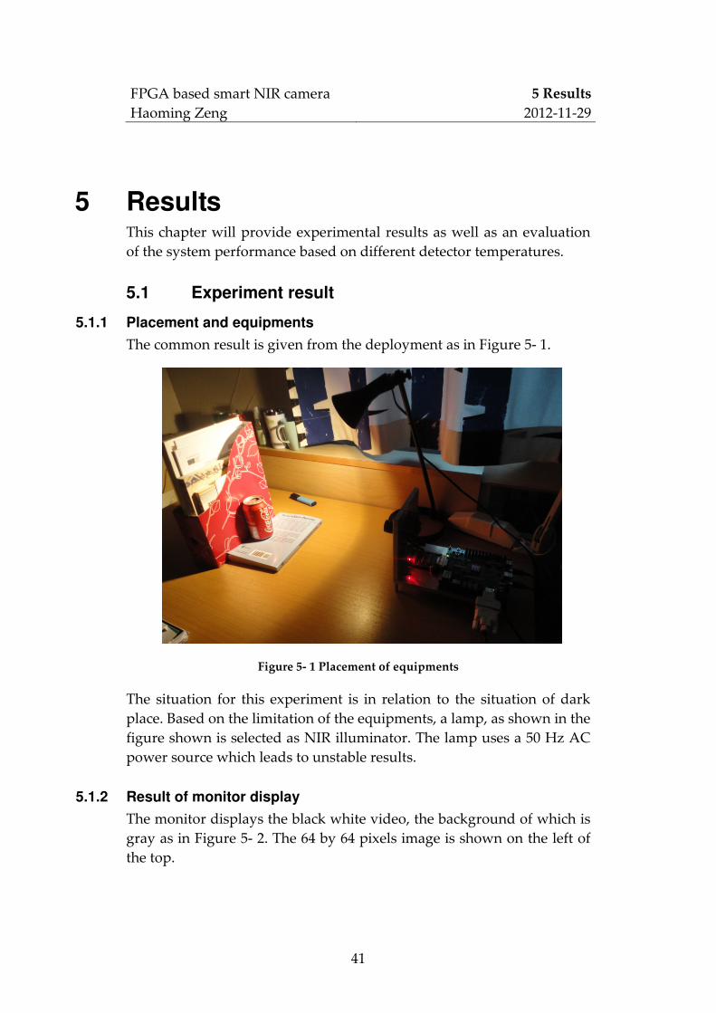
5.1.1 Placement and equipments ........................................... 41
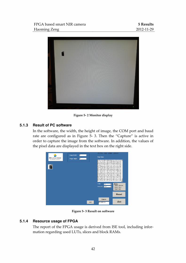
5.1.2 Result of monitor display .............................................. 41
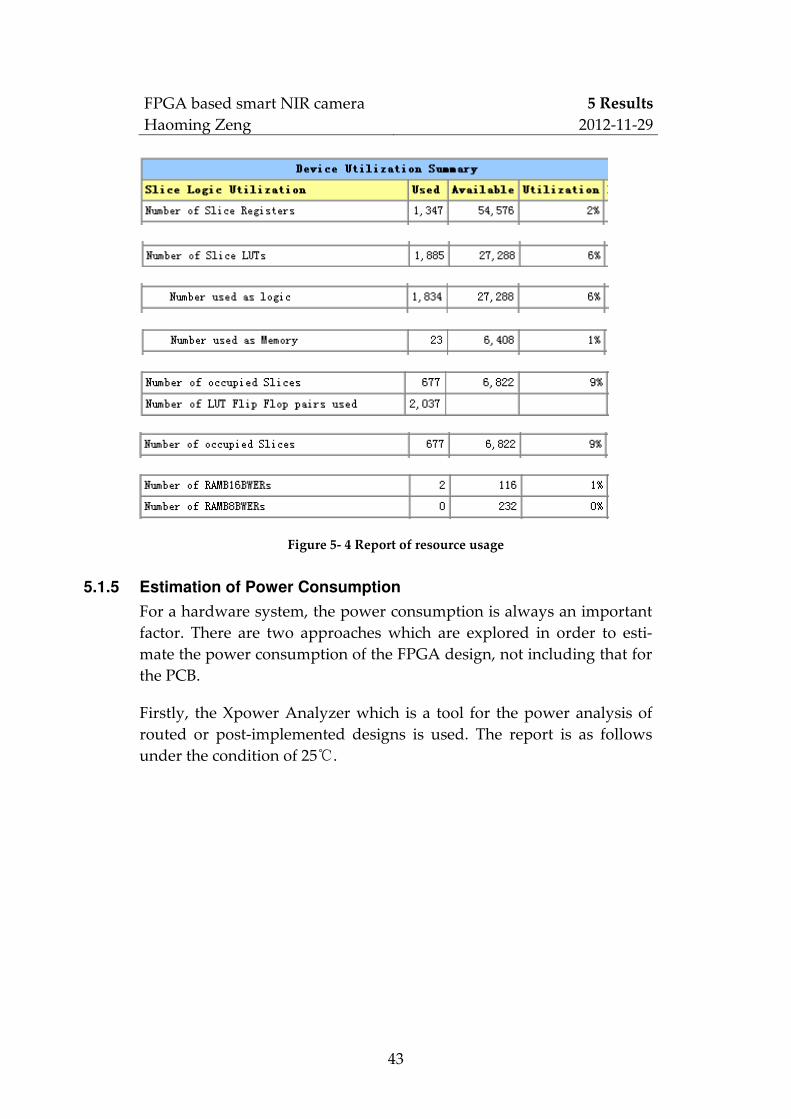
5.1.3 Result of PC software ..................................................... 42
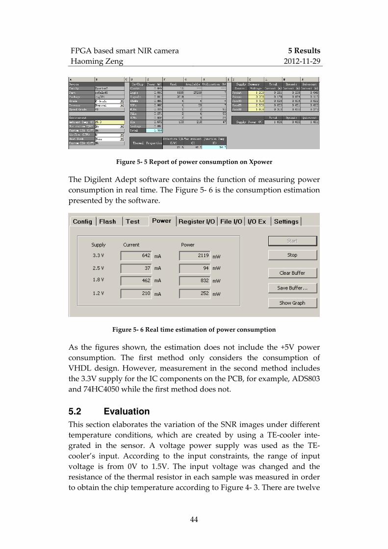
5.1.4 Resource usage of FPGA ............................................... 42
5.1.5 Estimation of Power Consumption .............................. 43
5.2 Evaluation ................................................................................... 44
6 Discussion ............................................................................................. 51
7 Conclusions .......................................................................................... 53
References ........................................................................................................ 55
Appendix A: Documentation of own developed program code ........... 57
VHDL code for NIR sensor reading (NIRReadout) ................................... 57
Pixels of NIR image generation (videoGen.vhd) ........................................ 59
VB software code ............................................................................................. 61
FPGA based smart NIR camera
Haoming Zeng
Terminology / Notation
2012-11-29
vi
Terminology / Notation
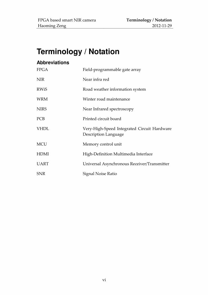
Abbreviations
FPGA Field-programmable gate array
NIR Near infra red
RWiS Road weather information system
WRM Winter road maintenance
NIRS Near Infrared spectroscopy
PCB Printed circuit board
VHDL Very-High-Speed Integrated Circuit Hardware
Description Language
MCU Memory control unit
HDMI High-Definition Multimedia Interface
UART Universal Asynchronous Receiver/Transmitter
SNR Signal Noise Ratio
FPGA based smart NIR camera
Haoming Zeng
List of Figures
2012-11-29
vii
List of Figures Figure 3- 1 Abstract of system architecture ........................................... 7
Figure 3- 3 Stereogram of implementation ........................................... 8
Figure 3- 2 Components of system ......................................................... 8
Figure 3- 4 Architecture of PCB .............................................................. 9
Figure 3- 5 Architecture of VHDL implementation ............................. 9
Figure 3- 7 Deployment of equipments ............................................... 10
Figure 3- 6 Software architecture .......................................................... 10
Figure 4- 1 NIR sensor [13] .................................................................... 13
Figure 4- 2 CMOS readout circuit ......................................................... 14
Figure 4- 3 Thermistor temperature characteristic ............................. 15
Figure 4- 4 Cooling characteristic of TE-cooler ................................... 15
Figure 4- 5 Current VS voltage .............................................................. 15
Figure 4- 6 Specifications of TE-cooler ................................................. 16
Figure 4- 7 ATLYS Board ....................................................................... 16
Figure 4- 8 ATLYS Board Components................................................ 17
Figure 4- 9 VHDC connector ................................................................. 18
Figure 4- 10 NIR Sensor Library ........................................................... 18
Figure 4- 11 Circuit for 4.5V power generator .................................... 19
Figure 4- 12 ADS803 converter circuit ................................................. 19
Figure 4- 13 ADC reference voltage circuit ......................................... 20
Figure 4- 14 Circuit for 2.5V generation ............................................... 20
Figure 4- 15 Circuit for -5V generation ................................................ 21
Figure 4- 16 Digital level characters ..................................................... 22
Figure 4- 17 Overview of the device ..................................................... 23
Figure 4- 18 Male board schematic ....................................................... 24
Figure 4- 19 Female board schematic ................................................... 24
Figure 4- 20 Layers specification ........................................................... 25
Figure 4- 21 Overview of PCB design .................................................. 26
Figure 4- 22 Different power source of PCB design ........................... 26
Figure 4- 24 PCB outline dimension ..................................................... 27
Figure 4- 23 The dimension of VHDCP connector ............................. 27
Figure 4- 25 Manufactured PCB design ............................................... 29
Figure 4- 26 Metal base of device .......................................................... 30
Figure 4- 27 NIR sensor dimension ...................................................... 30
Figure 4- 28 Holds on vertical metal board ......................................... 31
Figure 4- 29 End product of project ...................................................... 31
FPGA based smart NIR camera
Haoming Zeng
List of Figures
2012-11-29
viii
Figure 4- 30 Timing chart of NIR sensor .............................................. 32
Figure 4- 31 Timing diagram of ADS803 ............................................. 32
Figure 4- 32 Work flow of NIR controller ............................................ 33
Figure 4- 33 Entity of NIR controller .................................................... 33
Figure 4- 34 Frame buffer architecture ................................................. 34
Figure 4- 35 HDMI interface .................................................................. 35
Figure 4- 36 Entity of HDMI controller ................................................ 36
Figure 4- 37 UART Entity ....................................................................... 36
Figure 4- 38 Software GUI ..................................................................... 37
Figure 4- 39 GUI on running ................................................................. 38
Figure 4- 40 Basic work flow of software ............................................ 39
Figure 5- 1 Placement of equipments ................................................... 41
Figure 5- 2 Monitor display ................................................................... 42
Figure 5- 3 Result on software ............................................................... 42
Figure 5- 4 Report of resource usage .................................................... 43
Figure 5- 5 Report of power consumption on Xpower ...................... 44
Figure 5- 6 Real time estimation of power consumption .................. 44
Figure 5- 7 The placement of equipments ........................................... 45
Figure 5- 8 A captured image ................................................................ 46
Figure 5- 9 Diagrams of meanA, meanB, meanA-meanB and stdA 48
Figure 5- 10 tendency chart of images’ SNR ....................................... 48
Figure 5- 11 Histograms of region A and B ......................................... 49
Figure 5- 12 Maximum value of region A and minimum value of
region B ............................................................................................. 50
FPGA based smart NIR camera
Haoming Zeng
1 Introduction
2012-11-29
1
1 Introduction The report addresses an approach to developing an FPGA-based hard-
ware framework integrating NIR sensor. The background of the project
is in relation to the monitoring of winter road conditions. Additionally,
according to NIR technology, the system is also able to be applied in
other applications which will also be introduced. In this chapter, the
background and the motivation behind the project will be presented.
Furthermore an overall aim and the problems associated with the pro-
ject are stated. An outline of the thesis will also be given at the end of
this chapter.
1.1 Background and problem motivation
Road traffic safety always draws people’s attention, since road traffic
forms major part in the daily lives of many people and thus is directly
related to them. In order to improve road traffic safety, the detection of
the road condition has now become a crucial issue. It is essential that
official departments do take necessary measures to ensure safety as far
as possible. Road weather information system (RWiS) is one of the
world’s most widely implemented weather information services for
road traffic [1], providing information, such as radar and satellite im-
ages, which is given in real time to WRM personnel. The Swedish RWiS
has more than 600 roadside stations equipped with sensors, which are
able to measure several metrological variables [2]. The UK spends £482
million on the primary road network, while £1069 million is the cost
involved for winter maintenance of local roads [3]. Based on a study of
many cases, it is obviously that it is essential to have timely knowledge
of road condition.
Over the years, based on the inventions and applications relating to high
level technology and the maintenance personnel’s action, road traffic
safety has been improved and the traffic accident rate has been reduced
in many countries [3]. However, the problem do still exists.
There are many factors which can lead to traffic accidents, such as
sudden illness, drink driving etc. The slipperiness of the road is one of
the most dangerous situations, especially in northern regions such as
Sweden, Finland etc. where the low temperature can easily cause slipery

FPGA based smart NIR camera
Haoming Zeng
1 Introduction
2012-11-29
2
road. For example, in Finland, about 25% of all fatal accidents occur on
icy and snowy road surfaces [2]. Additionally, in Edmonton, Canada,
40% of the traffic accidents occur due to ice/snow or rain covering road
[3]. It is thus extremely important that the maintenance personnel pay
sufficient attention and perform suitable and timely actions on the
WRM. It is also necessary to inform the road users of abnormal road
situations in order to reduce the risk of traffic accidents.
The serious problem caused by the slipperiness of the road is always the
result of the formation of icy patches which will readily occurred after
rain or snow on a frosty road. It is caused by an objective factor, which
can be avoided, if sufficient measures are taken. However, a bad situa-
tion is faced that when the ice on road is thin and thus may be difficult
to observe but which is extremely dangerous. Under these conditions,
highly accurate and highly efficiency methods are always required.
Knowledge relating to the road surface temperature provides important
information with regards to an ice slipperiness warning system. Hence,
in this paper, a system based on NIR technology is proposed in order to
solve this problem and an evaluation of it will also be made.
Historically, in 1800, Herschel used a prism to separate the electromag-
netic spectrum and thus was able to discover the NIR region. In the
early 1920s, many NIR experiments were carried out, but it was not
widely applied until the mid 1960s. The potential of the NIR technique
was realized by Karl Norris and he used technique in an industrial field
under the name “Morden NIRS”. The reason why the NIR technology
was utilized based on its important features. Infrared light has a longer
wavelength than visible light and its wavelength corresponds to a
frequency range approximately 1 to 400 THz, and includes most of
thermal radiation emitted by objects [4]. Based on the principle, the
system is able to manage the monitoring of the road surface.
NIRS (Near Infrared spectroscopy) is a method based on molecular
overtone and combination vibrations. The absorption bands are promi-
nent in NIR region in relation to the -CH, -NH, -OH, -SH functional
group. NIRS technique covers both the wavelength range adjacent to
the mid infrared and the visible region. Based on this technique, the
proposed system can provide a sense of the situation relating to ice and
water.

FPGA based smart NIR camera
Haoming Zeng
1 Introduction
2012-11-29
3
NIR has also been applied practically in areas, including agriculture,
remote monitoring, medical uses, material science etc [5].
In terms of the platform and based on the rapid development of silicon
technology, FPGA has been chosen due to its high performance and
high capacity features which make it suitable for a complex hardware
design such as image processing.
1.2 Overall aim
This thesis project’s overall aim is to develop a primary hardware
framework for an NIR camera in relation to capturing, storing and
displaying images. In addition, an analysis of the images will also be
evaluated.
According to the proposal, the overall aim is divided into four parts to
show more detail.
● Develop an interface PCB board for NIR image sensor
● VHDL implementation for display and communication with PC
● Software design on PC for storage
● Analyse the generated images by NIR sensor
1.3 Problem statement
In this thesis project, during the design of the interface board, the prob-
lems associated with the type of required circuit are studied. The solu-
tion for this includes a high speed amplifier, high speed AD conversion
circuit and 5V and 3.3V logic level conversion circuits. In addition, a
compatible connector for ATLYS FPGA board should be carried, which
has an influence on the thickness and shape of the PCB board.
In terms of VHDL implementation, the problems arise from the control
of the NIR sensor and the pixels generation, communication with the PC
via the UART protocol, and the display of the images on an HDMI
monitor. During the programming, the delay of the AD conversion
should also be considered.
In software design, the problems that send the command to FPGA and
receive data and save the image as a BMP file should be solved. A
FPGA based smart NIR camera
Haoming Zeng
1 Introduction
2012-11-29
4
highly robust system, friendly GUI and low error rate of receiving data
are required for the software thus requiring many tests.
After the hardware structure has been designed and the PCB manufac-
tured, the soldering components onto the PCB also requires a strategy to
be adopted in order to ensure that each part works in a satisfactory
manner. Finally, an investigation is processed to evaluate the images’
quality under a variation in temperature.
1.4 Contribution
The FPGA platform operates with functions for monitor displaying and
a mechanism for frame buffering, which are provided by my supervisor
Benny Thörnberg. The function of UART communication has been
performed by Ashkan Hashemi, while the function of the sensor readout
and some modifications to the UART communication are conducted by
the author of this report.
The VB software and PCB are also designed by the author. Some of the
circuits for the PCB design have been provided by the author’s supervi-
sor. Additionally, the assembling of device has been performed with
assistance from author’s supervisor.
1.5 Outline
Chapter 2 states the related work of the project;
Chapter 3 provides a model for the system. Additionally, the PCB,
FPGA implementation and software’s architecture will be illustrated.
Chapter 4 elaborates the procedures during the implementation and
provides the detail of the design.
The result is presented in Chapter 5 and a conclusion/discussion is given
in Chapter 6.
FPGA based smart NIR camera
Haoming Zeng
2 Related work
2012-11-29
5
2 Related work Many methods have been exploited in recent years for road traffic safety.
For northern regions, the slipperiness of road problem is the out-
standing problem and a mounted sensor is one approach to studying it.
It is possible to forecast the frost on the road surface which may lead to
it becoming slippery [6].
Furthermore, there is a comparison between a passive and active sensor
made by Patrik Jonsson for road detection consideration [7]. He also
conducted research combining meteorological sensors and camera
images from RWiS in order to improve the road condition classification
[8]. Methods such as neural networks [8], Support Vector Machines
(SVM) [9], multivariate analysis [10] and etc are also studied.
All objects emit energies called thermal radiation due to its temperature
and IR is sensitive to this. Based on this feature, many applications have
been developed such as night vision devices, thermal imaging, commu-
nications and etc [11].
According to the research, IR has a higher reliability than mounted
sensors when applied to surface temperature reading during wet,
snowy or icy road conditions [12]. Additionally, NIR is one kind of IR
with 0.75um to 1.4um wavelength. NIR technology has been used in
freezing point detection in some cases [13]. Thus the NIR technology is
dedicate to this project’s development.

FPGA based smart NIR camera
Haoming Zeng
2 Related work
2012-11-29
6

FPGA based smart NIR camera
Haoming Zeng
3 Methodology
2012-11-29
7
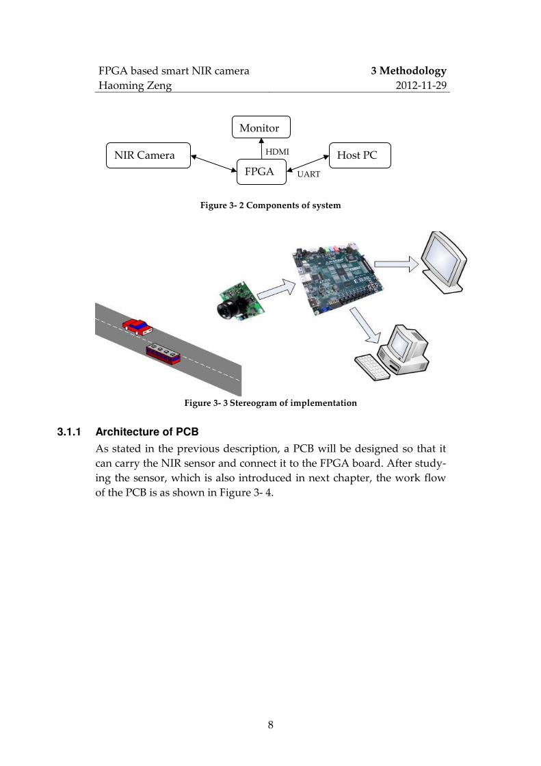
3 Methodology The purpose of the system is elaborated in the previous chapter and
thus the architecture of the whole system will be described.
The whole system basic operation flow chart is shown as Figure 3- 1:
Figure
1) Image capture: NIR sensor is planned to be applied for image
capturing. It is necessary to design a PCB board to
read out the data from the sensor.
2) Image processing: This step is realized in the FPGA board for which
ATLYS is chosen. Displaying the images on an
HDMI interface monitor is an essential part in or-
der to study the result. It also operates to send im-
age data to a host PC via UART protocol. This
process will be implemented in the FPGA board.
3) Further processing: Finally, it is able to restore,save and display the
image after receiving data from the second step.
Hence the image can be used for analysis, for in-
stance, by using MATLAB. The functions will be
realized by means of the software on a PC.
After analysing the functions of each part, the architecture can be de-
fined as the diagram Figure 3- 2 and the stereogram Figure 3- 3.
Image capture Image processing Further processing
Figure 3- 1 Abstract of system architecture
FPGA based smart NIR camera
Haoming Zeng
3 Methodology
2012-11-29
8
Figure 3- 3 Stereogram of implementation
3.1.1 Architecture of PCB
As stated in the previous description, a PCB will be designed so that it
can carry the NIR sensor and connect it to the FPGA board. After study-
ing the sensor, which is also introduced in next chapter, the work flow
of the PCB is as shown in Figure 3- 4.
NIR Camera
FPGA
Monitor
Host PC HDMI
UART
Figure 3- 2 Components of system
FPGA based smart NIR camera
Haoming Zeng
3 Methodology
2012-11-29
9
Figure 3- 4 Architecture of PCB
3.1.2 Architecture of FPGA implementation
VHDL is the language used for the FPGA implementation. The func-
tions for this part are to receive the data from the sensor, generate pixel
data and a timing sequence, display the captured images on monitor
with an HDMI interface, and communicate with a host PC via USB.
Accordingly, the general architecture of FPGA system is as shown in
Figure 3- 5.
Figure
3.1.3 Architecture of software
The software is used for receiving data and saving them into a file on the
PC.
Some demands were required after due consideration. Firstly, GUI is
necessary for the user’s convenience. The port and bound rate is select-
able in the interface. Other functions such as displaying the received
NIR Controller Frame Buffer
DDR2 on Board
NIR Camera Monitor
PC
Control read
Save read
HDMI Protocol
UART Protocol
FPGA Implementation
Figure 3- 5 Architecture of VHDL implementation
FPGA based smart NIR camera
Haoming Zeng
3 Methodology
2012-11-29
10
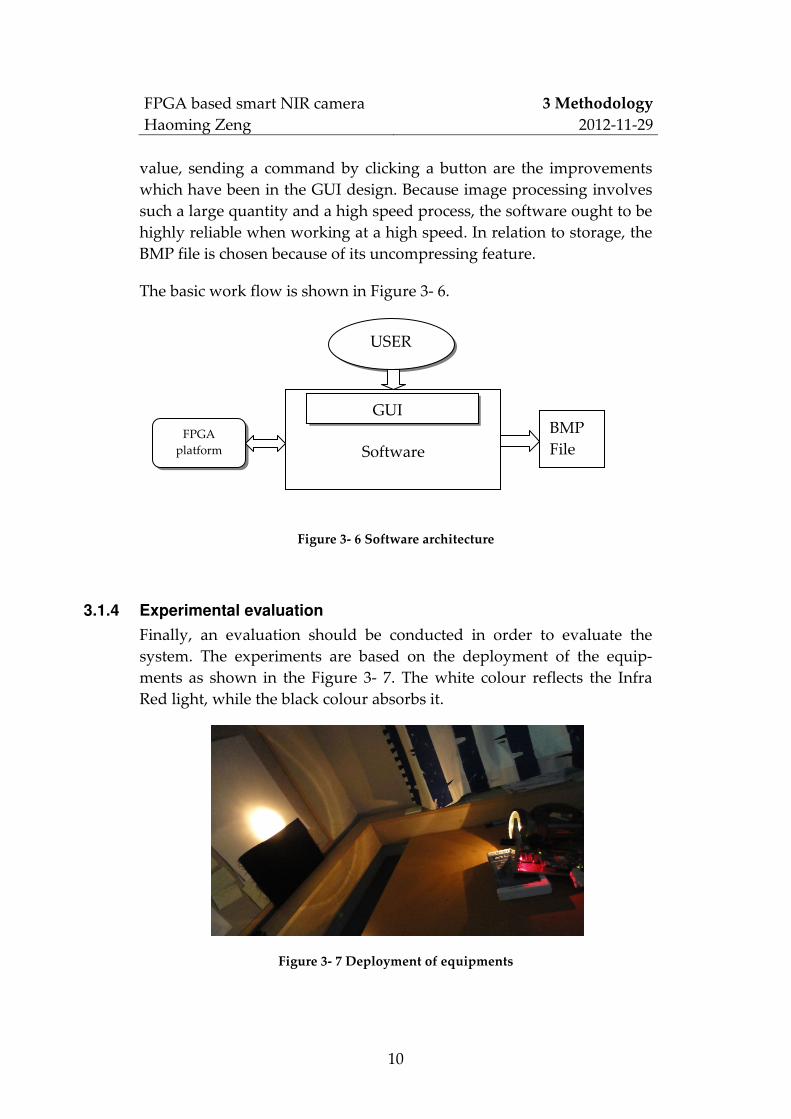
value, sending a command by clicking a button are the improvements
which have been in the GUI design. Because image processing involves
such a large quantity and a high speed process, the software ought to be
highly reliable when working at a high speed. In relation to storage, the
BMP file is chosen because of its uncompressing feature.
The basic work flow is shown in Figure 3- 6.
3.1.4 Experimental evaluation
Finally, an evaluation should be conducted in order to evaluate the
system. The experiments are based on the deployment of the equip-
ments as shown in the Figure 3- 7. The white colour reflects the Infra
Red light, while the black colour absorbs it.
Figure 3- 7 Deployment of equipments
USER
GUI
Software FPGA
platform
BMP
File
Figure 3- 6 Software architecture

FPGA based smart NIR camera
Haoming Zeng
3 Methodology
2012-11-29
11
It is thus able to capture an image for which half is white and the other
half black. The region A, obtained from the white part, is the foreground
and B, obtained from black part, is background. After the calculations by
means of the formula below, the SNR of images can be known. The
calculation will be conducted by using MATLAB.
SNR = (meanA-meanB)/stdA
Formula- 1 SNR calculation
According to the feather of the NIR detector, it integrates a one stage
cooler, which is able to control the detector’s temperature and a thermis-
tor by which the temperature is known after measurements are taken
according to Figure 4- 3. Hence, it is possible to study the variations of
the SNR with the changing of the sensor’s temperature.
Additionally, after compilation by means of an ISE tool, a report will be
generated which provides the information of FPGA usage, including
the used LUTs and the slices and block RAMs. The Xpower Analyzer,
which is integrated in the ISE tool and is a tool for the power analysis of
routed or post-implemented designs, is used. The Digilent Adept soft-
ware contains the function of measuring the power consumption in real
time. These three tools will provide more details in relation to the sys-
tem.

FPGA based smart NIR camera
Haoming Zeng
3 Methodology
2012-11-29
12
FPGA based smart NIR camera
Haoming Zeng
4 Design / Implementation
2012-11-29
13
4 Design / Implementation This chapter focuses on the implementation of the system including
schematic and layout design for the PCB, soldering components onto
PCB, the assembling of the device, the FPGA implementation and the
software design. However, before this, an introduction of the hardware
components is essential for further understanding.
4.1 Hardware introduction
4.1.1 NIR sensor
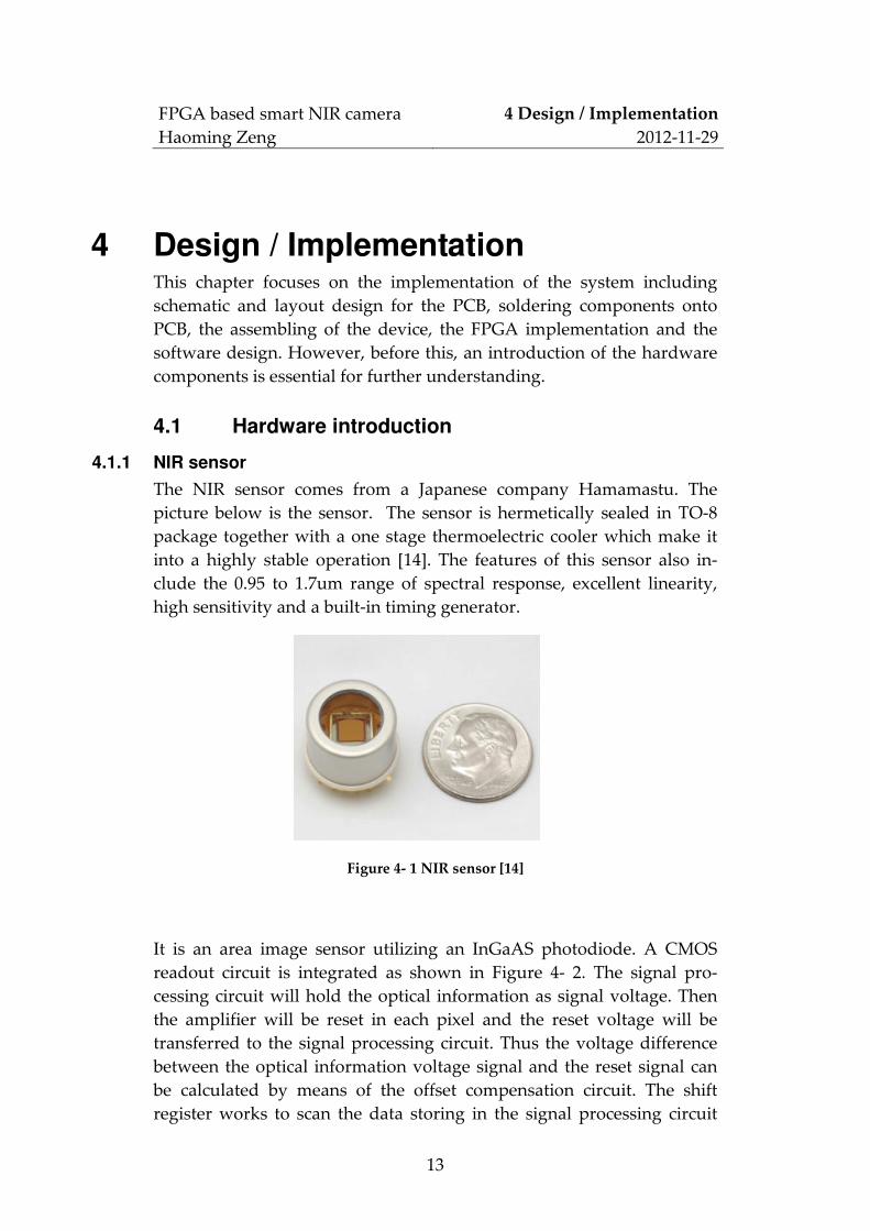
The NIR sensor comes from a Japanese company Hamamastu. The
picture below is the sensor. The sensor is hermetically sealed in TO-8
package together with a one stage thermoelectric cooler which make it
into a highly stable operation [14]. The features of this sensor also in-
clude the 0.95 to 1.7um range of spectral response, excellent linearity,
high sensitivity and a built-in timing generator.
Figure 4- 1 NIR sensor [14]
It is an area image sensor utilizing an InGaAS photodiode. A CMOS
readout circuit is integrated as shown in Figure 4- 2. The signal pro-
cessing circuit will hold the optical information as signal voltage. Then
the amplifier will be reset in each pixel and the reset voltage will be
transferred to the signal processing circuit. Thus the voltage difference
between the optical information voltage signal and the reset signal can
be calculated by means of the offset compensation circuit. The shift
register works to scan the data storing in the signal processing circuit
FPGA based smart NIR camera
Haoming Zeng
4 Design / Implementation
2012-11-29
14
from right to left. The image sensor is able to generate 64 by 64 pixels’
two dimensional infrared imaging. Each pixel size is 50*50 um and the
image size is 3.2*3.2mm. Thus an optical lens is required to in order to
obtain a wider visual field.
Figure 4- 2 CMOS readout circuit
The sensor can also be applied in many applications, for instance, ther-
mal imaging monitor, laser beam profiler and near infrared image
detection which are listed in its datasheet.
Because a one stage cooler is integrated in the image sensor, an evalua-
tion will take advantage of it in order to investigate the operation of the
system under various temperature conditions.
According to the purpose of the project, the system may work in ex-
treme environments. The cooler is able to control the sensor’s tempera-
ture during the operation of the system so as to ensure the quality of the
results. Hence, from the experiments, it is important to study the impact
of the cooler. In the datasheet, three diagrams are given as follows in
order to illustrate how to select the input power source.

FPGA based smart NIR camera
Haoming Zeng
4 Design / Implementation
2012-11-29
15
Figure 4- 3 Thermistor temperature characteristic
Figure 4- 4 Cooling characteristic of TE-cooler
Figure 4- 5 Current VS voltage
According to Figure 4- 3, Figure 4- 4 and Figure 4- 5, it can be seen that a
constant voltage power source can be given in order to adjust the tem-
FPGA based smart NIR camera
Haoming Zeng
4 Design / Implementation
2012-11-29
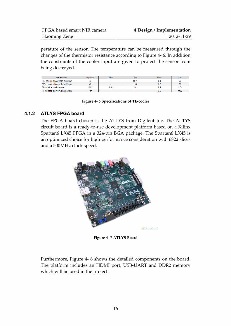
16
perature of the sensor. The temperature can be measured through the
changes of the thermistor resistance according to Figure 4- 6. In addition,
the constraints of the cooler input are given to protect the sensor from
being destroyed.
Figure 4- 6 Specifications of TE-cooler
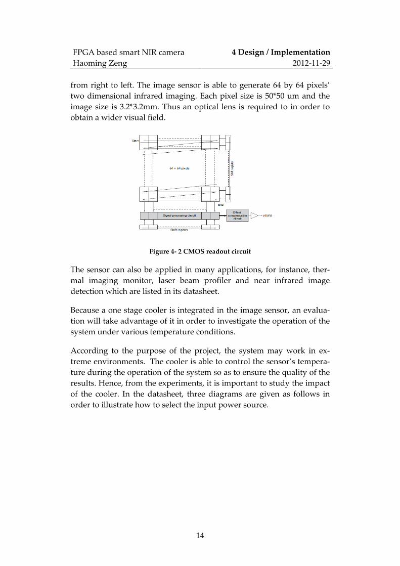
4.1.2 ATLYS FPGA board
The FPGA board chosen is the ATLYS from Digilent Inc. The ALTYS
circuit board is a ready-to-use development platform based on a Xilinx
Spartan6 LX45 FPGA in a 324-pin BGA package. The Spartan6 LX45 is
an optimized choice for high performance consideration with 6822 slices
and a 500MHz clock speed.
Figure 4- 7 ATLYS Board
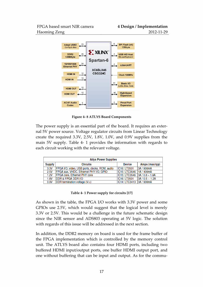
Furthermore, Figure 4- 8 shows the detailed components on the board.
The platform includes an HDMI port, USB-UART and DDR2 memory
which will be used in the project.
FPGA based smart NIR camera
Haoming Zeng
4 Design / Implementation
2012-11-29
17
Figure 4- 8 ATLYS Board Components
The power supply is an essential part of the board. It requires an exter-
nal 5V power source. Voltage regulator circuits from Linear Technology
create the required 3.3V, 2.5V, 1.8V, 1.0V, and 0.9V supplies from the
main 5V supply. Table 4- 1 provides the information with regards to
each circuit working with the relevant voltage.
Table 4- 1 Power supply for circuits [17]
As shown in the table, the FPGA I/O works with 3.3V power and some
GPIOs use 2.5V, which would suggest that the logical level is merely
3.3V or 2.5V. This would be a challenge in the future schematic design
since the NIR sensor and ADS803 operating at 5V logic. The solution
with regards of this issue will be addressed in the next section.
In addition, the DDR2 memory on board is used for the frame buffer of
the FPGA implementation which is controlled by the memory control
unit. The ATLYS board also contains four HDMI ports, including two
buffered HDMI input/output ports, one buffer HDMI output port, and
one without buffering that can be input and output. As for the commu-
FPGA based smart NIR camera
Haoming Zeng
4 Design / Implementation
2012-11-29
18
nication with the PC, there is an USB-UART bridge provided on board,
allowing the board to communicate with the PC based on a UART
protocol. On the PC, a driver for this bridge from EXRA should be
installed.
In order to connect the FPGA platform and the NIR camera, the expan-
sion connector must be studied in order to design an interface with the
PCB. Figure 4- 9 shows the connector’s general view. The black dots are
connected to the ground.
Figure 4- 9 VHDC connector
4.2 PCB design
4.2.1 Schematic design
Based on the information previously introduced, first of all, the schemat-
ic should be designed for this PCB board in order to provide an interface
between the sensor and the FPGA board. In the previous chapter, the
survey of the design has been discussed. The schematic for each part
will be illustrated in the following section.
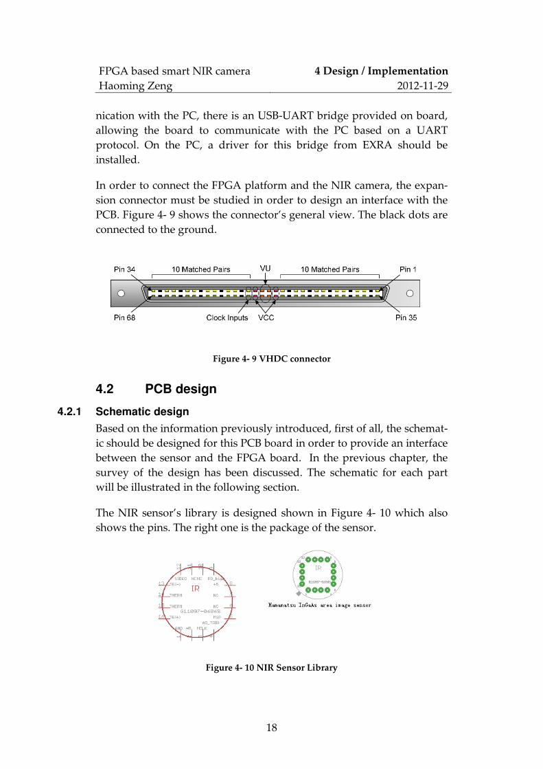
The NIR sensor’s library is designed shown in Figure 4- 10 which also
shows the pins. The right one is the package of the sensor.
Figure 4- 10 NIR Sensor Library
FPGA based smart NIR camera
Haoming Zeng
4 Design / Implementation
2012-11-29
19
As shown in Figure 4- 10, MSP is the signal for starting a new frame and
for determining the exposure time. The AD_TROG indication of the
output voltage is the pixel value. MCLK is the working clock with a
maximal 40MHz. PD_bias requires a 4.5V power source. The circuit
shown in Figure 4- 11 is able to achieve this value by adjusting the
potential meter.
Figure 4- 11 Circuit for 4.5V power generator
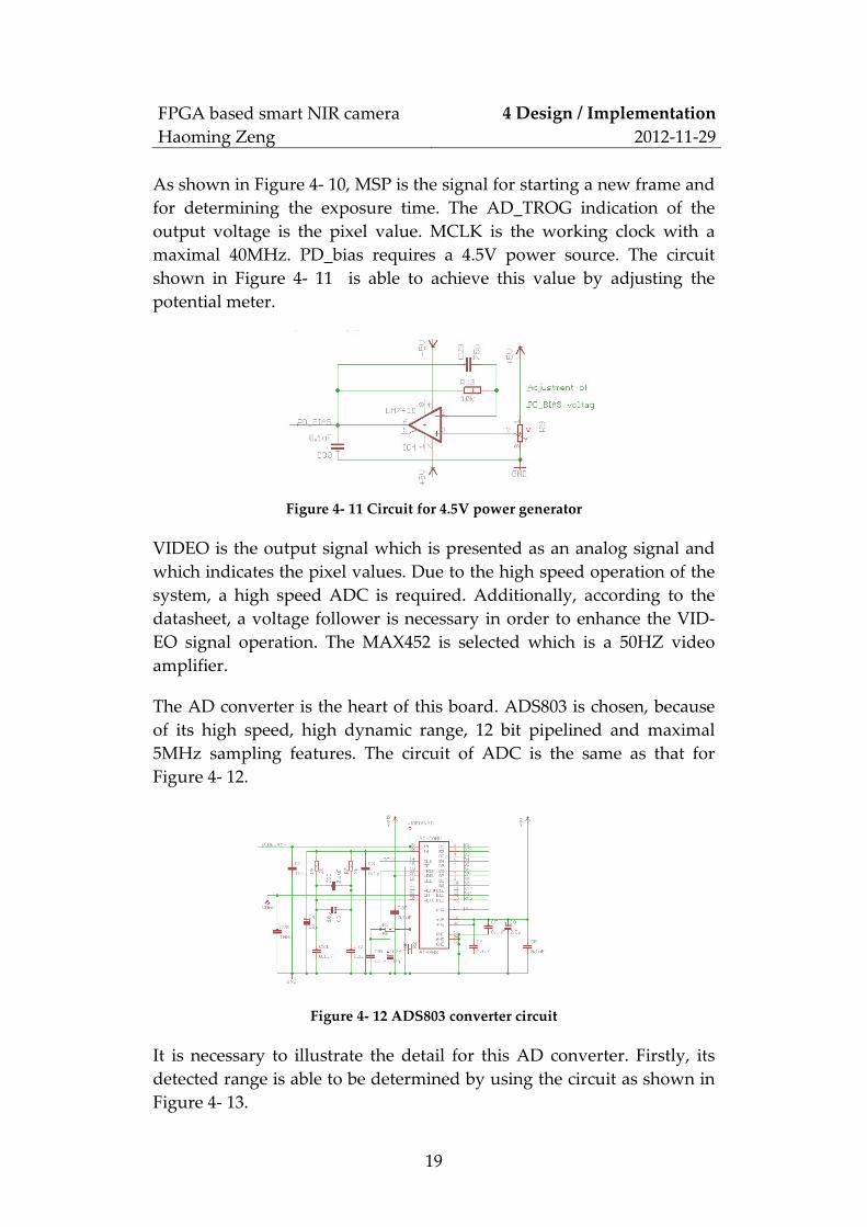
VIDEO is the output signal which is presented as an analog signal and
which indicates the pixel values. Due to the high speed operation of the
system, a high speed ADC is required. Additionally, according to the
datasheet, a voltage follower is necessary in order to enhance the VID-
EO signal operation. The MAX452 is selected which is a 50HZ video
amplifier.
The AD converter is the heart of this board. ADS803 is chosen, because
of its high speed, high dynamic range, 12 bit pipelined and maximal
5MHz sampling features. The circuit of ADC is the same as that for
Figure 4- 12.
Figure 4- 12 ADS803 converter circuit
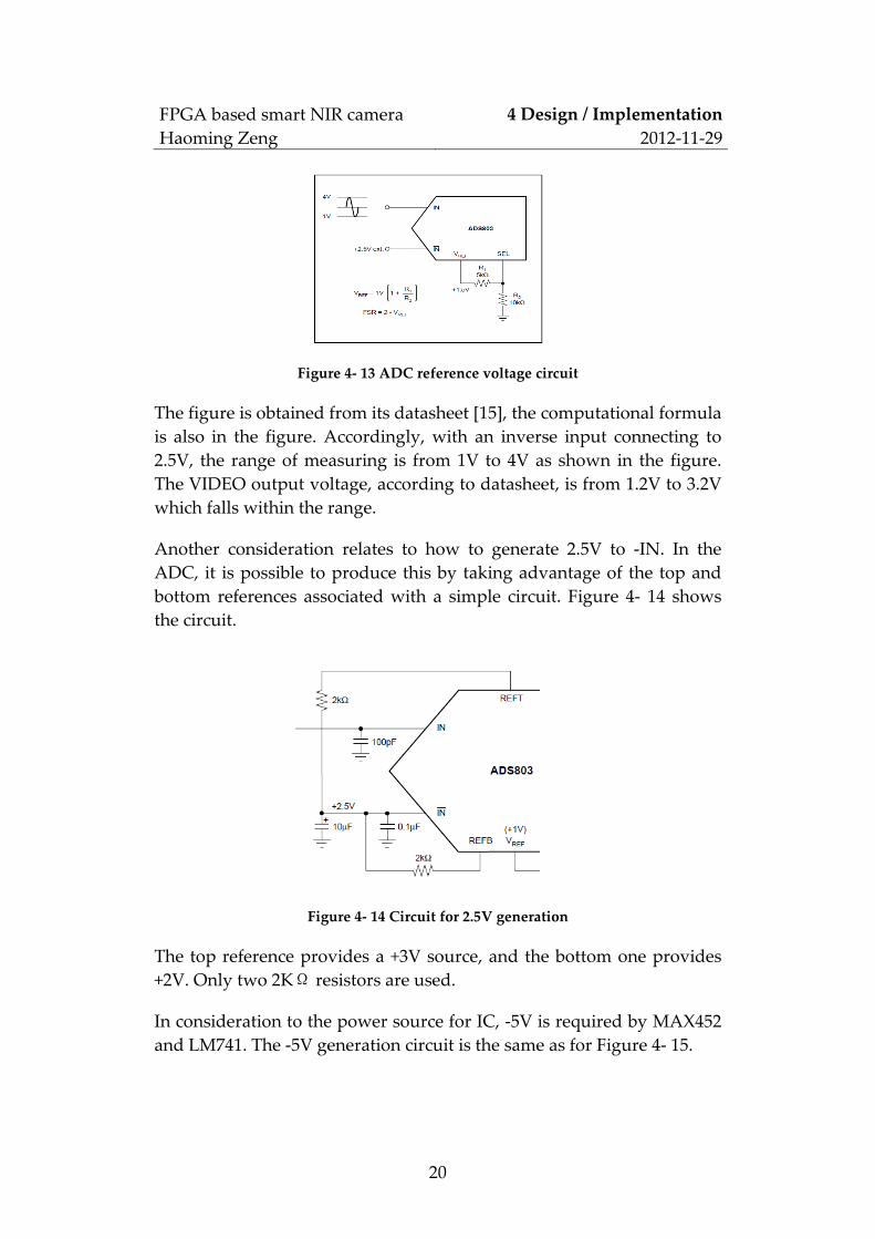
It is necessary to illustrate the detail for this AD converter. Firstly, its
detected range is able to be determined by using the circuit as shown in
Figure 4- 13.
FPGA based smart NIR camera
Haoming Zeng
4 Design / Implementation
2012-11-29
20
Figure 4- 13 ADC reference voltage circuit
The figure is obtained from its datasheet [15], the computational formula
is also in the figure. Accordingly, with an inverse input connecting to
2.5V, the range of measuring is from 1V to 4V as shown in the figure.
The VIDEO output voltage, according to datasheet, is from 1.2V to 3.2V
which falls within the range.
Another consideration relates to how to generate 2.5V to -IN. In the
ADC, it is possible to produce this by taking advantage of the top and
bottom references associated with a simple circuit. Figure 4- 14 shows
the circuit.
Figure 4- 14 Circuit for 2.5V generation
The top reference provides a +3V source, and the bottom one provides
+2V. Only two 2KΩ resistors are used.
In consideration to the power source for IC, -5V is required by MAX452
and LM741. The -5V generation circuit is the same as for Figure 4- 15.
FPGA based smart NIR camera
Haoming Zeng
4 Design / Implementation
2012-11-29
21
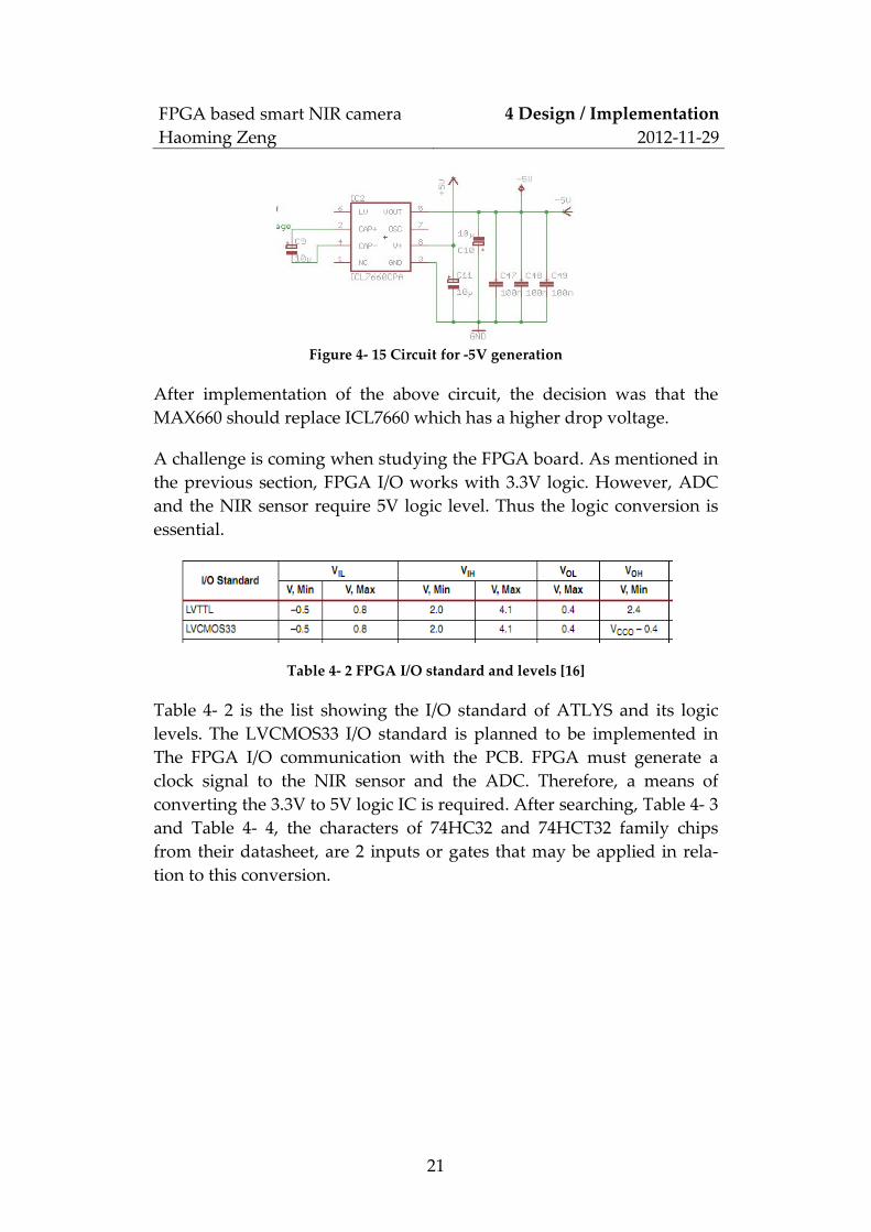
Figure 4- 15 Circuit for -5V generation
After implementation of the above circuit, the decision was that the
MAX660 should replace ICL7660 which has a higher drop voltage.
A challenge is coming when studying the FPGA board. As mentioned in
the previous section, FPGA I/O works with 3.3V logic. However, ADC
and the NIR sensor require 5V logic level. Thus the logic conversion is
essential.
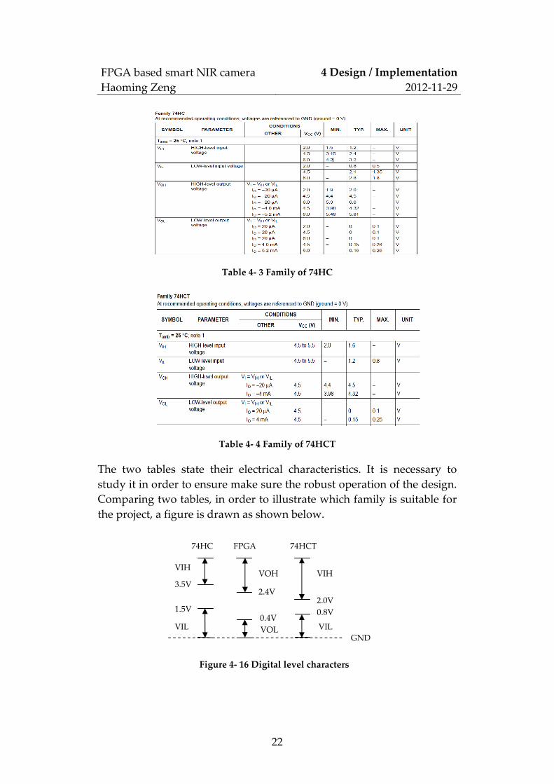
Table 4- 2 FPGA I/O standard and levels [16]
Table 4- 2 is the list showing the I/O standard of ATLYS and its logic
levels. The LVCMOS33 I/O standard is planned to be implemented in
The FPGA I/O communication with the PCB. FPGA must generate a
clock signal to the NIR sensor and the ADC. Therefore, a means of
converting the 3.3V to 5V logic IC is required. After searching, Table 4- 3
and Table 4- 4, the characters of 74HC32 and 74HCT32 family chips
from their datasheet, are 2 inputs or gates that may be applied in rela-
tion to this conversion.
FPGA based smart NIR camera
Haoming Zeng
4 Design / Implementation
2012-11-29
22
Table 4- 3 Family of 74HC
Table 4- 4 Family of 74HCT
The two tables state their electrical characteristics. It is necessary to
study it in order to ensure make sure the robust operation of the design.
Comparing two tables, in order to illustrate which family is suitable for
the project, a figure is drawn as shown below.
3.5V
1.5V
VIH
VIL
74HC FPGA
VOH
2.4V
0.4V
VOL
2.0V
0.8V
GND
74HCT
VIL
VIH
Figure 4- 16 Digital level characters
FPGA based smart NIR camera
Haoming Zeng
4 Design / Implementation
2012-11-29
23
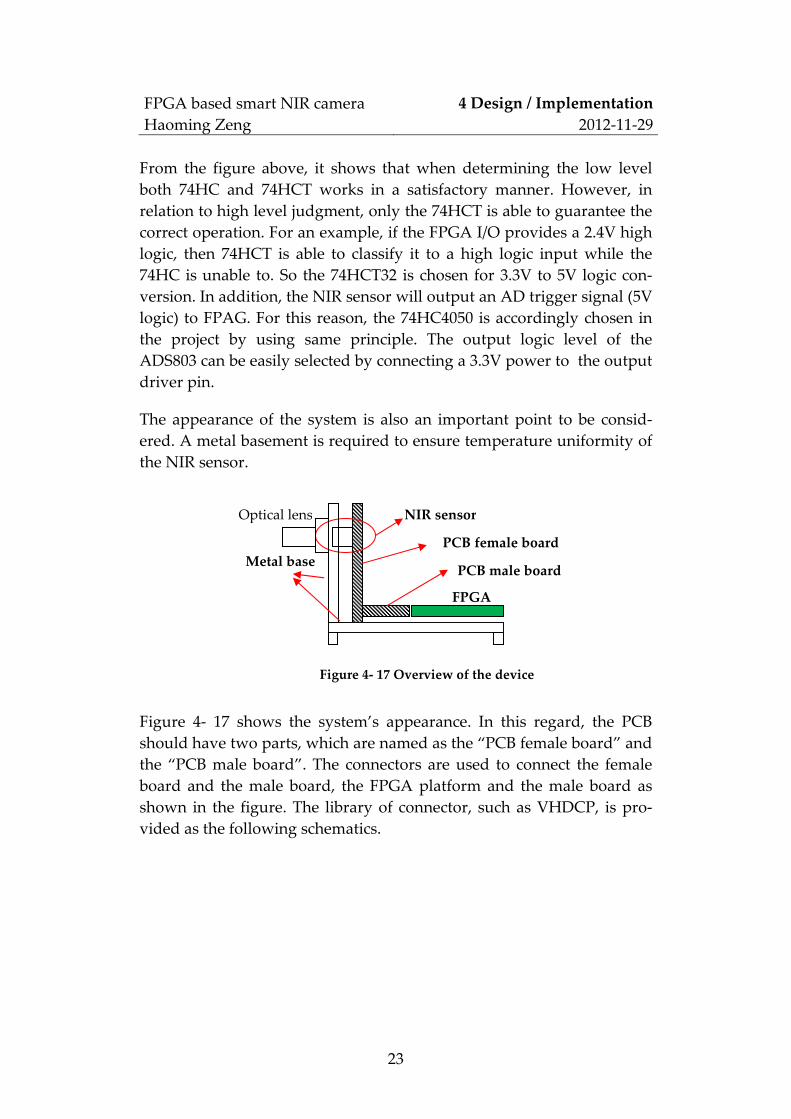
From the figure above, it shows that when determining the low level
both 74HC and 74HCT works in a satisfactory manner. However, in
relation to high level judgment, only the 74HCT is able to guarantee the
correct operation. For an example, if the FPGA I/O provides a 2.4V high
logic, then 74HCT is able to classify it to a high logic input while the
74HC is unable to. So the 74HCT32 is chosen for 3.3V to 5V logic con-
version. In addition, the NIR sensor will output an AD trigger signal (5V
logic) to FPAG. For this reason, the 74HC4050 is accordingly chosen in
the project by using same principle. The output logic level of the
ADS803 can be easily selected by connecting a 3.3V power to the output
driver pin.
The appearance of the system is also an important point to be consid-
ered. A metal basement is required to ensure temperature uniformity of
the NIR sensor.
Figure 4- 17 shows the system’s appearance. In this regard, the PCB
should have two parts, which are named as the “PCB female board” and
the “PCB male board”. The connectors are used to connect the female
board and the male board, the FPGA platform and the male board as
shown in the figure. The library of connector, such as VHDCP, is pro-
vided as the following schematics.
FPGA
NIR sensor
PCB female board
PCB male board Metal base
Optical lens
Figure 4- 17 Overview of the device
FPGA based smart NIR camera
Haoming Zeng
4 Design / Implementation
2012-11-29
24
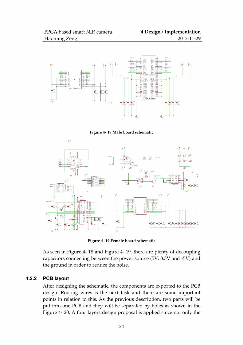
Figure 4- 18 Male board schematic
Figure 4- 19 Female board schematic
As seen in Figure 4- 18 and Figure 4- 19, there are plenty of decoupling
capacitors connecting between the power source (5V, 3.3V and -5V) and
the ground in order to reduce the noise.
4.2.2 PCB layout
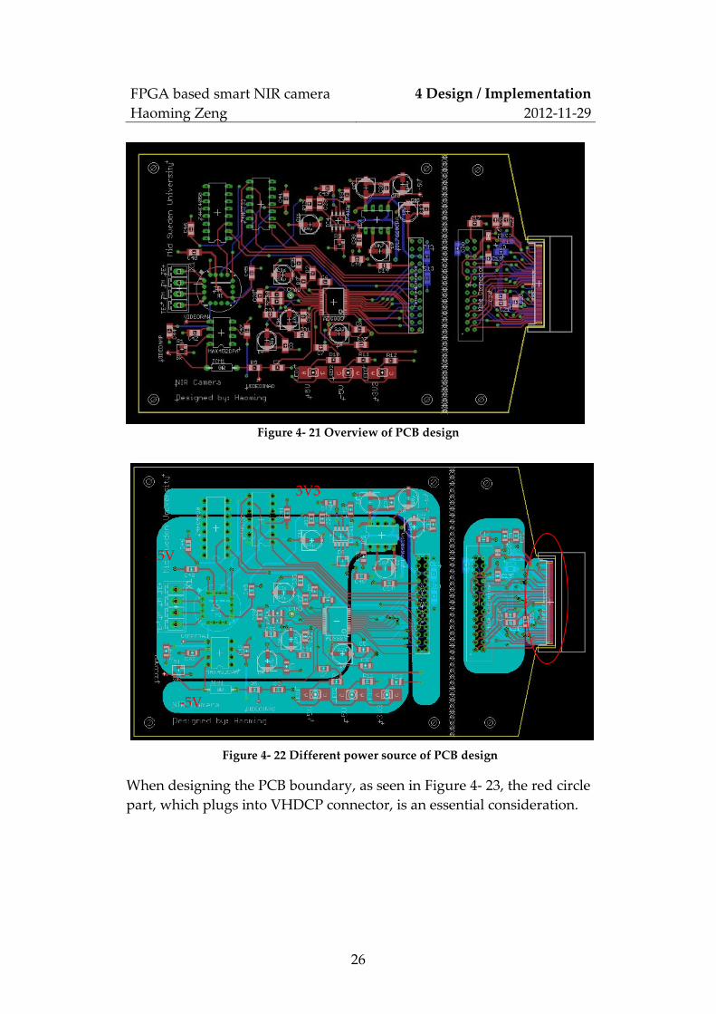
After designing the schematic, the components are exported to the PCB
design. Rooting wires is the next task and there are some important
points in relation to this. As the previous description, two parts will be
put into one PCB and they will be separated by holes as shown in the
Figure 4- 20. A four layers design proposal is applied since not only the
FPGA based smart NIR camera
Haoming Zeng
4 Design / Implementation
2012-11-29
25
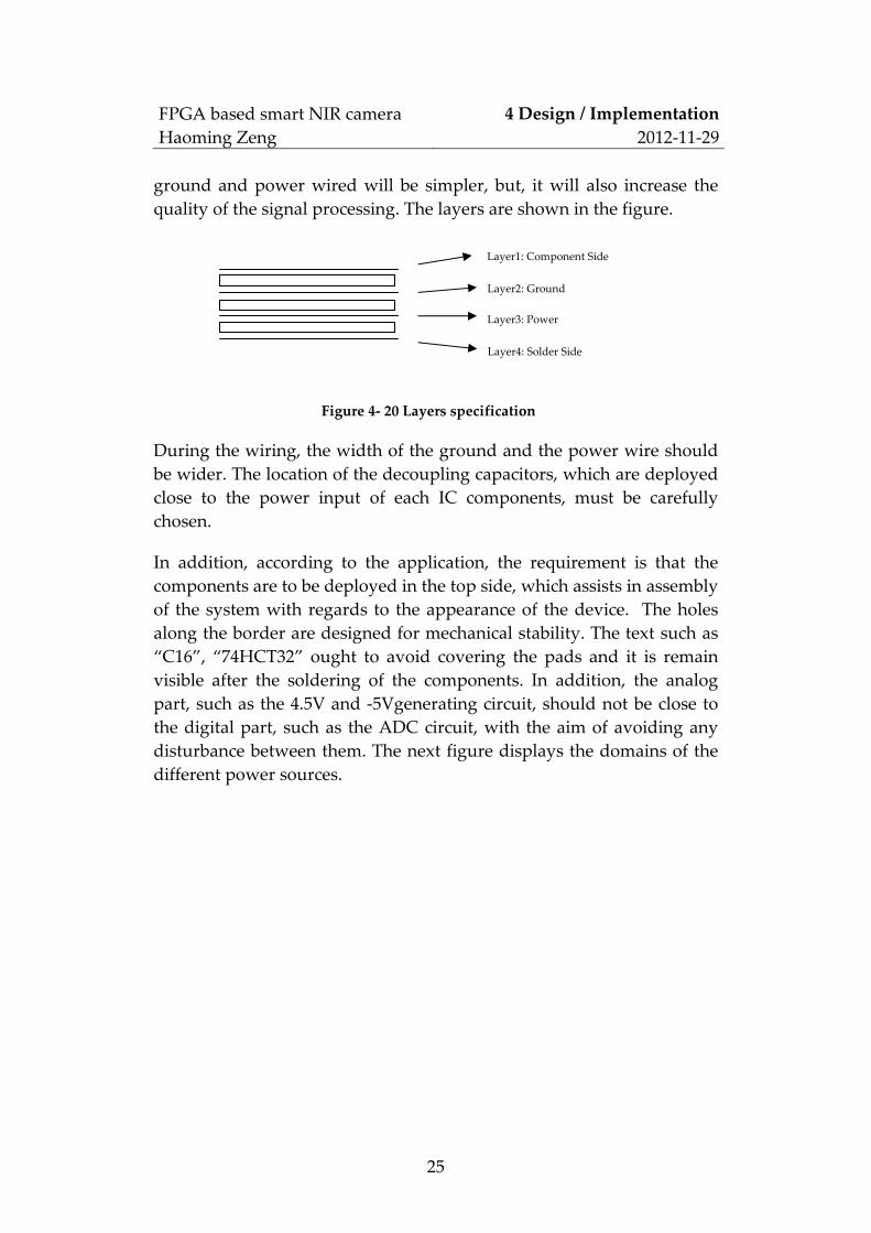
ground and power wired will be simpler, but, it will also increase the
quality of the signal processing. The layers are shown in the figure.
During the wiring, the width of the ground and the power wire should
be wider. The location of the decoupling capacitors, which are deployed
close to the power input of each IC components, must be carefully
chosen.
In addition, according to the application, the requirement is that the
components are to be deployed in the top side, which assists in assembly
of the system with regards to the appearance of the device. The holes
along the border are designed for mechanical stability. The text such as
“C16”, “74HCT32” ought to avoid covering the pads and it is remain
visible after the soldering of the components. In addition, the analog
part, such as the 4.5V and -5Vgenerating circuit, should not be close to
the digital part, such as the ADC circuit, with the aim of avoiding any
disturbance between them. The next figure displays the domains of the
different power sources.
Layer1: Component Side
Layer2: Ground
Layer3: Power
Layer4: Solder Side
Figure 4- 20 Layers specification
FPGA based smart NIR camera
Haoming Zeng
4 Design / Implementation
2012-11-29
26
Figure 4- 21 Overview of PCB design
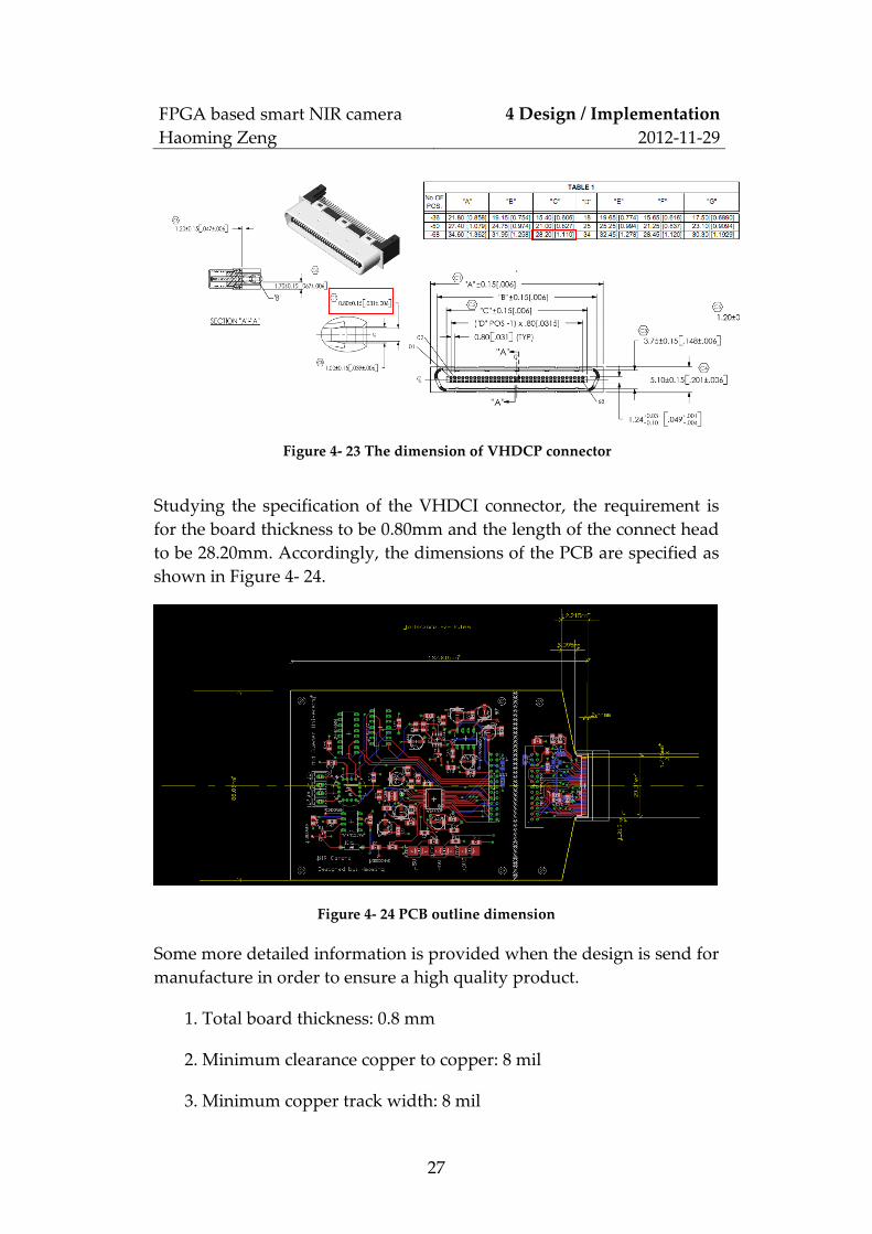
When designing the PCB boundary, as seen in Figure 4- 23, the red circle
part, which plugs into VHDCP connector, is an essential consideration.
5V
3V3
-5V
Figure 4- 22 Different power source of PCB design
FPGA based smart NIR camera
Haoming Zeng
4 Design / Implementation
2012-11-29
27
Studying the specification of the VHDCI connector, the requirement is
for the board thickness to be 0.80mm and the length of the connect head
to be 28.20mm. Accordingly, the dimensions of the PCB are specified as
shown in Figure 4- 24.
Figure 4- 24 PCB outline dimension
Some more detailed information is provided when the design is send for
manufacture in order to ensure a high quality product.
1. Total board thickness: 0.8 mm
2. Minimum clearance copper to copper: 8 mil
3. Minimum copper track width: 8 mil
Figure 4- 23 The dimension of VHDCP connector
FPGA based smart NIR camera
Haoming Zeng
4 Design / Implementation
2012-11-29
28
4. Copper thickness for Layer1 and Layer 4: min 18 um
5. Copper thickness for Layer2 and Layer 3: min 35 um
6. Material: FR4
7. Design tool version: “Eagle 5.11.0 Professional”. Board file
NIRversion11.brd is supplied as reference.
Furthermore, the files listed in Table 4- 5 are required by the factory.
File
extension
Used for Layer
.cmp Copper tracks, Vias, Pads Layer 1, Component side
.ly2 Ground plane, Vias, Pads Layer2
.ly3 Power supply plane, Vias, Pads Layer3
.sol Copper tracks, Vias, Pads Layer 4, Solder side
.plc Printing Silkscreen on component side
.pls Printing Silkscreen on solder side
.stc Solder stop mask Solder stop mask on component side
.sts Solder stop mask Solder stop mask on solder side
.drd Drills, Holes Drill data
.lyx Cutting of board edges Physical board outline drawing
Table 4- 5 Required files and its specification
Figure 4- 25 shows the actual appearance after manufacturing.
FPGA based smart NIR camera
Haoming Zeng
4 Design / Implementation
2012-11-29
29
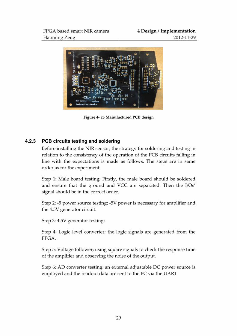
Figure 4- 25 Manufactured PCB design
4.2.3 PCB circuits testing and soldering
Before installing the NIR sensor, the strategy for soldering and testing in
relation to the consistency of the operation of the PCB circuits falling in
line with the expectations is made as follows. The steps are in same
order as for the experiment.
Step 1: Male board testing; Firstly, the male board should be soldered
and ensure that the ground and VCC are separated. Then the I/Os’
signal should be in the correct order.
Step 2: -5 power source testing; -5V power is necessary for amplifier and
the 4.5V generator circuit.
Step 3: 4.5V generator testing;
Step 4: Logic level converter; the logic signals are generated from the
FPGA.
Step 5: Voltage follower; using square signals to check the response time
of the amplifier and observing the noise of the output.
Step 6: AD converter testing; an external adjustable DC power source is
employed and the readout data are sent to the PC via the UART
FPGA based smart NIR camera
Haoming Zeng
4 Design / Implementation
2012-11-29
30
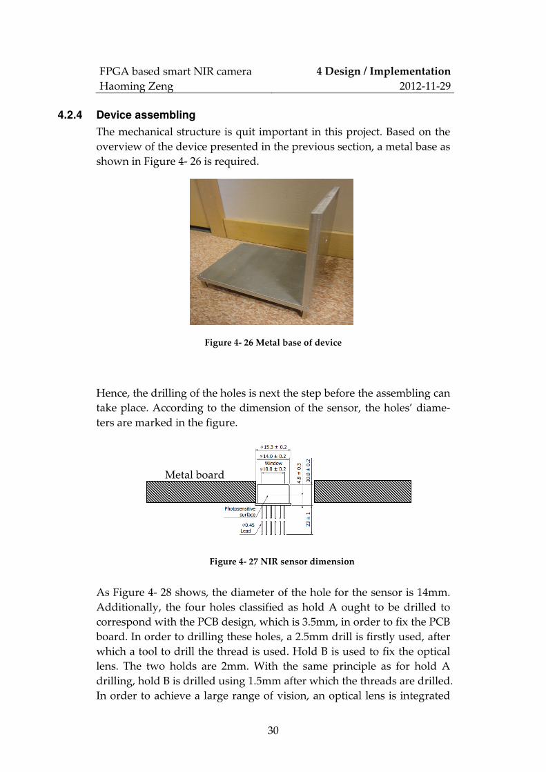
4.2.4 Device assembling
The mechanical structure is quit important in this project. Based on the
overview of the device presented in the previous section, a metal base as
shown in Figure 4- 26 is required.
Figure 4- 26 Metal base of device
Hence, the drilling of the holes is next the step before the assembling can
take place. According to the dimension of the sensor, the holes’ diame-
ters are marked in the figure.
As Figure 4- 28 shows, the diameter of the hole for the sensor is 14mm.
Additionally, the four holes classified as hold A ought to be drilled to
correspond with the PCB design, which is 3.5mm, in order to fix the PCB
board. In order to drilling these holes, a 2.5mm drill is firstly used, after
which a tool to drill the thread is used. Hold B is used to fix the optical
lens. The two holds are 2mm. With the same principle as for hold A
drilling, hold B is drilled using 1.5mm after which the threads are drilled.
In order to achieve a large range of vision, an optical lens is integrated
Metal board
Figure 4- 27 NIR sensor dimension
FPGA based smart NIR camera
Haoming Zeng
4 Design / Implementation
2012-11-29
31
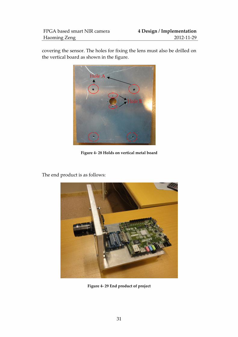
covering the sensor. The holes for fixing the lens must also be drilled on
the vertical board as shown in the figure.
Figure 4- 28 Holds on vertical metal board
The end product is as follows:
Figure 4- 29 End product of project
Hole A
Hole B

FPGA based smart NIR camera
Haoming Zeng
4 Design / Implementation
2012-11-29
32
4.3 VHDL implementation
The FPGA handles the image data from the sensor for displaying and
sending to the PC. As for the previous description of the VHDL imple-
mentation architecture, this part contains the NIR controller, Frame
Buffer, DDR signal processing, HDMI signal processing and UART
signal processing.
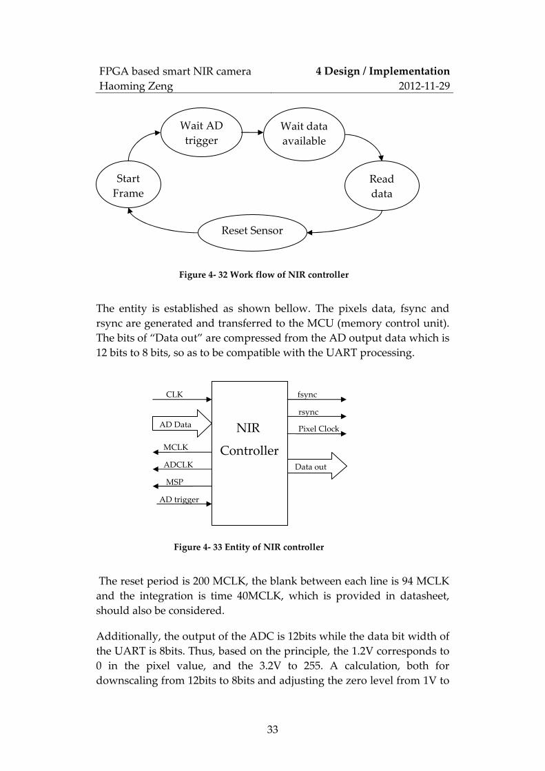
4.3.1 NIR controller implementation
The NIR controller outputs the clock signal, start signal to the NIR
sensor and the clock signal to the AD converter. The AD converter
generates 12 bits of data to the controller. Figure 4- 30 is the timing chart
of the sensor. Figure 4- 31 is the AD converter’s time diagram.
Figure 4- 30 Timing chart of NIR sensor
Figure 4- 31 Timing diagram of ADS803
After a new frame is started, which is triggered by MSP signal, a 90
MCLK blank period will follow. Then the NIR sensor will output the
AD trigger signal within the period of the 8 MCLK. When the AD trig-
ger’s signal is coming, the AD converter will generate the corresponding
data after 6 clock cycles of the AD. The step is named as “wait data
available”. According to this mechanism, the work flow is designed.
FPGA based smart NIR camera
Haoming Zeng
4 Design / Implementation
2012-11-29
33
The entity is established as shown bellow. The pixels data, fsync and
rsync are generated and transferred to the MCU (memory control unit).
The bits of “Data out” are compressed from the AD output data which is
12 bits to 8 bits, so as to be compatible with the UART processing.
The reset period is 200 MCLK, the blank between each line is 94 MCLK
and the integration is time 40MCLK, which is provided in datasheet,
should also be considered.
Additionally, the output of the ADC is 12bits while the data bit width of
the UART is 8bits. Thus, based on the principle, the 1.2V corresponds to
0 in the pixel value, and the 3.2V to 255. A calculation, both for
downscaling from 12bits to 8bits and adjusting the zero level from 1V to
CLK
AD Data
MCLK
ADCLK
MSP
AD trigger
fsync
rsync
Pixel Clock
Data out
NIR
Controller
Start
Frame
Wait AD
trigger
Wait data
available
Read
data
Reset Sensor
Figure 4- 32 Work flow of NIR controller
Figure 4- 33 Entity of NIR controller
FPGA based smart NIR camera
Haoming Zeng
4 Design / Implementation
2012-11-29
34
1.2V, is thus required. The formula is constructed in order to manage
this and is also applied in the VHDL project.
Equation (1): Din*(REFT-REFB)/2^12= Vadc - 1V
Equation (2): Dout*(VDmax-VDmin)/2^8= Vadc - VDmin
According to Equation 1 and 2, the formula is calculated as Formula 1.
Equation (3): Dout = Din*3/32 – 25.6
Formula- 2 Downscaling calculation
In the application, the REFT is 4V, and the REFB is 1V. Vadc is the
output voltage of the AD converter. VDmax is the maximum value of
the sensor’s output while VDmin is the minimum value. Din is the
integer value after conversion from the 12 bits value by the VHDL
function. Dout is converted to the 8bits value finally as the output for
the UART controller.
4.3.2 Frame Buffer
The frame buffer receives data from the NIR controller and stores them
into the DDR. And the HDMI and the UART controller will read out the
frame data out. These controlling processes are realized by the MCU.
As shown in the Figure 4- 34, the MCU has 3 ports. Port A reads data
from the NIR controller. Port B writes data into the DDR and reads them
out. Port C sends data to the UART or the HDMI which is chosen by the
Memory Control Unit
Port A Port B Port C
FIFO FIFO
NIR controller DDR HDMI UART
Frame buffer
FIFO
Figure 4- 34 Frame buffer architecture
FPGA based smart NIR camera
Haoming Zeng
4 Design / Implementation
2012-11-29
35
PC command. If the PC sends data to the FPGA, the data will be send
out to the PC via the UART. At the same time, the monitor will be
turned off. After a whole frame has been transferred to the PC, the
frame will be stored as a BMP file without compression, and the monitor
will work again. This module is designed by Digilent.
4.3.3 HDMI controller
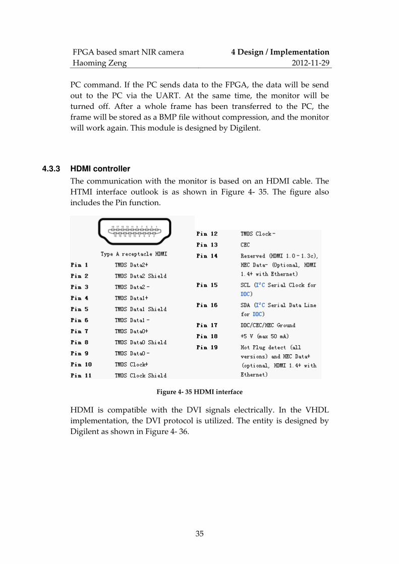
The communication with the monitor is based on an HDMI cable. The
HTMI interface outlook is as shown in Figure 4- 35. The figure also
includes the Pin function.
Figure 4- 35 HDMI interface
HDMI is compatible with the DVI signals electrically. In the VHDL
implementation, the DVI protocol is utilized. The entity is designed by
Digilent as shown in Figure 4- 36.

FPGA based smart NIR camera
Haoming Zeng
4 Design / Implementation
2012-11-29
36
4.3.4 UART controller
The UART controller is in charge of the communication with the PC.
When the PC sends a command to the FPGA, the image data will be
read from the Frame Buffer and sent to the PC by means of the UART
controller. The entity of the UART controller is as shown in Figure 4- 37.
The UART will set the PC_COMMAND to ‘1’ after receiving command
from the PC. The PC_COMMAND gives the command to the system to
disconnect the monitor, reset the Frame Buffer address pointer and
connect the Frame Buffer to the UART controller.
CLK FIFO_RESET
PC_COMMAND
RXD
TX_DATA
RESET
RD
UART
Controller
READY
WR
RX_FULL
RX_AVAIL
TX_BUSY
TX_AVAIL
TXD
RX_DATA
CLK TMDS_TX_CLK_P
TMDS_TX_CLK_N
SERSTB
SERCLK
Red (0 to 7)
Pixel Clock
HDMI
Controller
Green (0 to 7)
Blue (0 to 7)
2*Pixel Clock
TMDS_TX_2_P
TMDS_TX_2_N
TMDS_TX_1_P
TMDS_TX_1_N
TMDS_TX_0_N
TMDS_TX_0_N
Figure 4- 36 Entity of HDMI controller
Figure 4- 37 UART Entity
FPGA based smart NIR camera
Haoming Zeng
4 Design / Implementation
2012-11-29
37
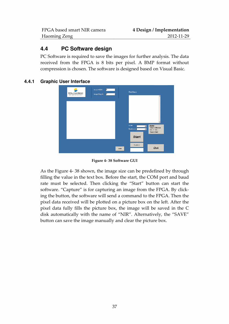
4.4 PC Software design
PC Software is required to save the images for further analysis. The data
received from the FPGA is 8 bits per pixel. A BMP format without
compression is chosen. The software is designed based on Visual Basic.
4.4.1 Graphic User Interface
Figure 4- 38 Software GUI
As the Figure 4- 38 shown, the image size can be predefined by through
filling the value in the text box. Before the start, the COM port and baud
rate must be selected. Then clicking the “Start” button can start the
software. “Capture” is for capturing an image from the FPGA. By click-
ing the button, the software will send a command to the FPGA. Then the
pixel data received will be plotted on a picture box on the left. After the
pixel data fully fills the picture box, the image will be saved in the C
disk automatically with the name of “NIR”. Alternatively, the “SAVE”
button can save the image manually and clear the picture box.
FPGA based smart NIR camera
Haoming Zeng
4 Design / Implementation
2012-11-29
38
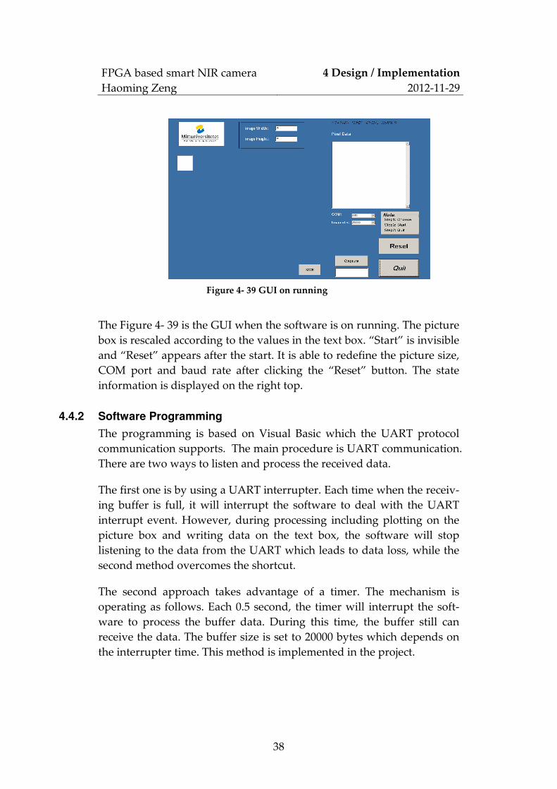
The Figure 4- 39 is the GUI when the software is on running. The picture
box is rescaled according to the values in the text box. “Start” is invisible
and “Reset” appears after the start. It is able to redefine the picture size,
COM port and baud rate after clicking the “Reset” button. The state
information is displayed on the right top.
4.4.2 Software Programming
The programming is based on Visual Basic which the UART protocol
communication supports. The main procedure is UART communication.
There are two ways to listen and process the received data.
The first one is by using a UART interrupter. Each time when the receiv-
ing buffer is full, it will interrupt the software to deal with the UART
interrupt event. However, during processing including plotting on the
picture box and writing data on the text box, the software will stop
listening to the data from the UART which leads to data loss, while the
second method overcomes the shortcut.
The second approach takes advantage of a timer. The mechanism is
operating as follows. Each 0.5 second, the timer will interrupt the soft-
ware to process the buffer data. During this time, the buffer still can
receive the data. The buffer size is set to 20000 bytes which depends on
the interrupter time. This method is implemented in the project.
Figure 4- 39 GUI on running

FPGA based smart NIR camera
Haoming Zeng
4 Design / Implementation
2012-11-29
39
Start
0.5 s?
Read data
from buffer
Picture box
full? Save image
No
No
Yes
Yes
Figure 4- 40 Basic work flow of software

FPGA based smart NIR camera
Haoming Zeng
4 Design / Implementation
2012-11-29
40
FPGA based smart NIR camera
Haoming Zeng
5 Results
2012-11-29
41
5 Results This chapter will provide experimental results as well as an evaluation
of the system performance based on different detector temperatures.
5.1 Experiment result
5.1.1 Placement and equipments
The common result is given from the deployment as in Figure 5- 1.
Figure 5- 1 Placement of equipments
The situation for this experiment is in relation to the situation of dark
place. Based on the limitation of the equipments, a lamp, as shown in the
figure shown is selected as NIR illuminator. The lamp uses a 50 Hz AC
power source which leads to unstable results.
5.1.2 Result of monitor display
The monitor displays the black white video, the background of which is
gray as in Figure 5- 2. The 64 by 64 pixels image is shown on the left of
the top.
FPGA based smart NIR camera
Haoming Zeng
5 Results
2012-11-29
42
Figure 5- 2 Monitor display
5.1.3 Result of PC software
In the software, the width, the height of image, the COM port and baud
rate are configured as in Figure 5- 3. Then the “Capture” is active in
order to capture the image from the software. In addition, the values of
the pixel data are displayed in the text box on the right side.
Figure 5- 3 Result on software
5.1.4 Resource usage of FPGA
The report of the FPGA usage is derived from ISE tool, including infor-
mation regarding used LUTs, slices and block RAMs.
FPGA based smart NIR camera
Haoming Zeng
5 Results
2012-11-29
43
Figure 5- 4 Report of resource usage
5.1.5 Estimation of Power Consumption
For a hardware system, the power consumption is always an important
factor. There are two approaches which are explored in order to esti-
mate the power consumption of the FPGA design, not including that for
the PCB.
Firstly, the Xpower Analyzer which is a tool for the power analysis of
routed or post-implemented designs is used. The report is as follows
under the condition of 25℃.
FPGA based smart NIR camera
Haoming Zeng
5 Results
2012-11-29
44
Figure 5- 5 Report of power consumption on Xpower
The Digilent Adept software contains the function of measuring power
consumption in real time. The Figure 5- 6 is the consumption estimation
presented by the software.
Figure 5- 6 Real time estimation of power consumption
As the figures shown, the estimation does not include the +5V power
consumption. The first method only considers the consumption of
VHDL design. However, measurement in the second method includes
the 3.3V supply for the IC components on the PCB, for example, ADS803
and 74HC4050 while the first method does not.
5.2 Evaluation
This section elaborates the variation of the SNR images under different
temperature conditions, which are created by using a TE-cooler inte-
grated in the sensor. A voltage power supply was used as the TE-
cooler’s input. According to the input constraints, the range of input
voltage is from 0V to 1.5V. The input voltage was changed and the
resistance of the thermal resistor in each sample was measured in order
to obtain the chip temperature according to Figure 4- 3. There are twelve

FPGA based smart NIR camera
Haoming Zeng
5 Results
2012-11-29
45
samples captured to analyze the variation of the SNR of the images as
the temperature changing.
In order to achieve high quality results, numerous measures have been
taken in order to reduce noise or disturbance as much as possible. The
experiments were conducted at night which can avoid the disturbance
from solar light, and the room lights are also turned off. Additionally, a
flashlight is used as the illuminator, because the flashlight uses DC
power which is better than the lamp using 50HZ AC. Although the
power consumed by the flashlight is rather pretty high and the experi-
ments will thus take a longer time, for the sake of maintaining the uni-
form of illumination, a constant DC power source is applied instead of
the battery. Figure 5- 7 is the experimental set up.
Figure 5- 7 The placement of equipments
The black colour can absorb the NIR, while the white can reflect it. After
the arrangement of the equipments, the images are captured as shown
in Figure 5- 8.
FPGA based smart NIR camera
Haoming Zeng
5 Results
2012-11-29
46
Figure 5- 8 A captured image
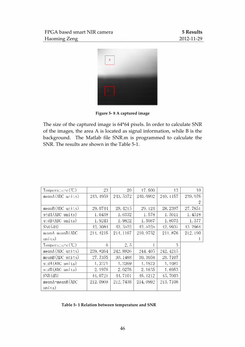
The size of the captured image is 64*64 pixels. In order to calculate SNR
of the images, the area A is located as signal information, while B is the
background. The Matlab file SNR.m is programmed to calculate the
SNR. The results are shown in the Table 5-1.
Temperature(℃) 23 20 17.500 13 10 meanA(ADC units) 243.4959 243.5372 240.0992 240.1157 239.9752 meanB(ADC units) 29.0744 29.4215 29.124 28.2397 27.7851 stdA(ADC units) 1.6438 1.6332 1.578 1.5011 1.4518 stdB(ADC units) 1.9243 1.9822 1.5087 1.8075 1.577 SNR(dB) 42.3084 42.3522 42.5225 42.9937 43.2964 meanA-meanB(ADC units) 214.4215 214.1157 210.9752 211.876 212.1901 Temperature(℃) 6 2.5 -1 -3 meanA(ADC units) 239.8264 242.8926 244.405 242.4215 meanB(ADC units) 27.7355 30.1488 30.3058 28.7107 stdA(ADC units) 1.3271 1.2369 1.1873 1.1087 stdB(ADC units) 2.1976 2.0276 2.1635 1.6953 SNR(dB) 44.0721 44.7101 45.1212 45.7003 meanA-meanB(ADC units) 212.0909 212.7438 214.0992 213.7108
Table 5- 1 Relation between temperature and SNR
FPGA based smart NIR camera
Haoming Zeng
5 Results
2012-11-29
47
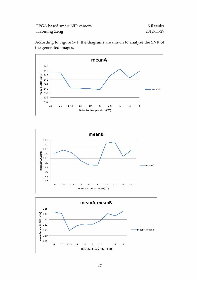
According to Figure 5- 1, the diagrams are drawn to analyze the SNR of
the generated images.
FPGA based smart NIR camera
Haoming Zeng
5 Results
2012-11-29
48
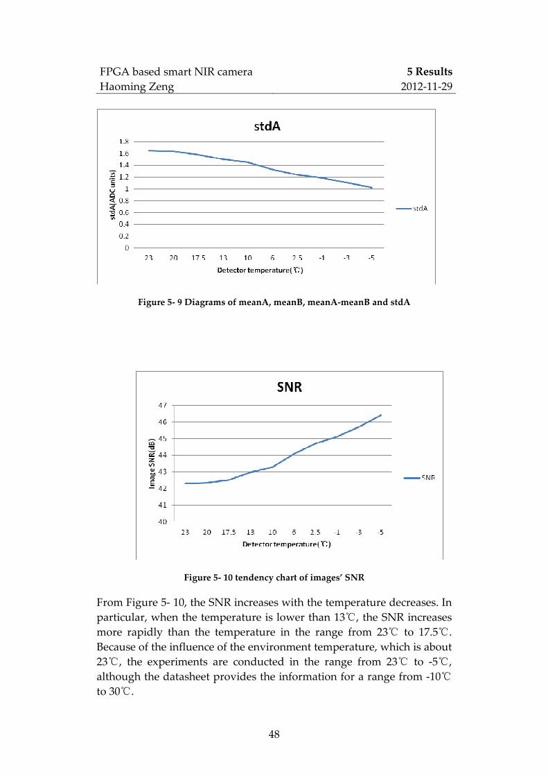
Figure 5- 9 Diagrams of meanA, meanB, meanA-meanB and stdA
Figure 5- 10 tendency chart of images’ SNR
From Figure 5- 10, the SNR increases with the temperature decreases. In
particular, when the temperature is lower than 13℃, the SNR increases
more rapidly than the temperature in the range from 23℃ to 17.5℃.
Because of the influence of the environment temperature, which is about
23℃, the experiments are conducted in the range from 23℃ to -5℃,
although the datasheet provides the information for a range from -10℃
to 30℃.

FPGA based smart NIR camera
Haoming Zeng
5 Results
2012-11-29
49
Temperature: 23℃
Temperature: -5℃
Figure 5- 11 Histograms of region A and B
Temperature: 23℃

FPGA based smart NIR camera
Haoming Zeng
5 Results
2012-11-29
50
Temperature: -5℃
Figure 5- 12 Maximum value of region A and minimum value of region B
In order to achieve a high quality evaluation, the Figure 5- 11 and Figure
5- 12 are posted so as to take the consideration of detector saturation
which will also have an influence on the image SNR, too. The analyze
will be described in the discussion part.
FPGA based smart NIR camera
Haoming Zeng
6 Discussion
2012-11-29
51
6 Discussion An FPGA based real time NIR camera is developed in this thesis project.
A PCB, including the considerations in relation to the logic level conver-
sion, power source generation, analog to digital signal conversion and
assembling of device, has been designed and verified successfully.
VHDL implementation enables the FPGA to readout the image data
from the sensor, display this on the monitor and send it to the PC. In
addition, the PC software has a friendly GUI and is full of the functions
required. The BMP file can be utilized in further processing.
The performance of the system has been evaluated under different
temperatures. From the result, it obviously shows that the system works
is in a satisfactory manner. It is also the case that the SNR of images are
boosted as the sensor’s temperature is decreasing. Although according
to the datasheet of the NIR sensor, there is a one stage cooler available,
which is able to control the sensor within the range of 30℃ to -10℃, the
room temperature might have an influence on that, which might be
because of a too high thermal resistance in the connection of the detector
metal to the cooler aluminium, which leads to the sensor temperature in
the range of 23℃ to -5℃ during the experiments.
Then the influence of the illumination should be analyzed. The parame-
ters drawn as shown in Figure 5- 9 will assist in this analysis.
MeanA is the mean value of the region A, which is treated as the
foreground and B is the background. The tendency of meanA and
meanB is related to the variations of the illumination’s intensity.
However, the signal=meanA–meanB still remained almost constant
during the entire measurement, with only a 1.6% variation. From the
tendency of stdB, it is known that the fluctuations of the background are
small. However, the noise represented by stdA decreases and the signal
= meanA-meanB increases as the temperature decreases. Thus the SNR
boosts as in the description in the result chapter.
Figure 5- 11 shows the histograms of regions A and B under the differ-
ent temperatures. After zooming in on the figures, the max value and
min value are the same as in Figure 5- 12. Thus the max value is
246.5(3.126V), and the min value is 24.5(1.39V) in -5℃. Comparing these
FPGA based smart NIR camera
Haoming Zeng
6 Discussion
2012-11-29
52
with the values at 23℃, it is thus known that the detector is saturated at
-5℃. According to the Formula- 1, meanA will abate leading to a reduc-
tion of the SNR.
Additionally, based on the limited conditions, the investigation was
conducted without measuring the temperature of the sensor. The resis-
tance of thermal resistor was measured in order to obtain the chip
temperature and then the results were recorded. In addition, the exper-
iments for the SNR investigation should avoid solar light. However, the
summer night is short while the experiments took a long time and thus
the evaluation of the SNR images under the variation of temperature
proved not to be as successful as was hoped.
In relation to the aim of detecting the ice or water covering on the road
surface, the experiments should be conducted in the future to attempt to
detect that by analyzing the images received. After verification, the
method will be integrated into the FPGA platform.
FPGA based smart NIR camera
Haoming Zeng
7 Conclusions
2012-11-29
53
7 Conclusions
With regards to the aim of exploiting a system for monitoring the
ice/water on road surface, the thesis has drawn an approach to develop
a hardware device based on NIR technology.
The NIR image sensor requires high speed processing which is able to
be managed by FPGA. The whole system contains three parts, including
the interface PCB, FPGA processing and host PC software. All the im-
plementations are described in the paper. The parts are accomplished
separated, and then the combination is performed successfully.
From the experiments, in general, the system does achieve the purpose
in relation to the building of the hardware structure. From the result, the
objects exist in the bmp image in accordance with the expectation. The
evaluation experiments were performed by utilizing a one stage cooler,
which was integrated into the NIR sensor. How the cooler affects on the
SNR images can also be studied. A metal base, will have an influence on
the system temperature uniformity, based on its thermal conductivity,
which was used to fix the system. However, it will enhance the system
performance.
A future continuance of this work should be to place the system into a
practical situation in which more disturbance factors exit. In addition,
the images stored in the PC should be analyzed by some method in
order to have knowledge as to that whether the ice/water is able to be
classified. Finally, the method may be applied into the FPGA platform to
make the system achieve the final goal.

FPGA based smart NIR camera
Haoming Zeng
2012-11-29
54
FPGA based smart NIR camera
Haoming Zeng
References
2012-11-29
55
References [1] Swedish Road Administration, “Road weather information sys-
tem”
[2] J. Norrman, M. Eriksson, and S. Lindqvist, ”Relationships be-
tween road slipperiness, traffic accident risk and winter road
maintenance activity,” September 5, 2000
[3] K. Andersson, ” Winter Road Conditions and Traffic Accidents
in Sweden and UK” 2010
[4] WuHan, “Infrared Introduction” 2010.
[5] C.-P. Sherman Hsu ,“Infrared Spectroscopy” 2010
[6] SIRWEC, A Guide to Road Weather Systems. 2007, Standing Inter-
national Road Weather Commission.
[7] P. Jonsson,” ROAD STATUS SENSORS A COMPARISON OF
ACTIVE AND PASSIVE SENSORS” Mid Sweden University,
2009
[8] P. Jonsson, "Road Condition Discrimination using Weather Data
and Camera Images," Unpublished, Mid Sweden University,
2010.
[9] P. Conrad, and M. Foedisch, "Performance evaluation of color
based road detection using neural nets and support vector ma-
chines." pp. 157-160, 2003.
[10] T. Li, S. Zhu, and M. Ogihara, “Using discriminant analysis for
multi-class classification: an experimental investigation,”
Knowledge and Information Systems, vol. 10, no. 4, pp. 453-472,
2006.
[11] J. VILLANUEVA ” Infrared Light” July 2009
[12] P. Jonsson,” Infrared Thermometry in winter road maintenance”
Mid Sweden University
FPGA based smart NIR camera
Haoming Zeng
References
2012-11-29
56
[13] W. Dehui, W. Xiaohong “Research on soft measuring for freez-
ing point of diesel fuel based on NIR spec-trometry” 2007
[14] “InGaAs area image sensor”, Hamamatsu, Sep, 2011
[15] “12-Bit, 5MHz Sampling ANALOG-TO-DIGITAL CONVERTER”,
Texas Instruments, Sep, 2002
[16] “Spartan-6 FPGA Data Sheet: DC and Switching Characteristics”,
Oct, 2011
[17] “Atlys reference manual”,
http://www.digilentinc.com/Products/Detail.cfm?NavPath=2,400,
836&Prod=ATLYS December 19, 2011

FPAG based smart NIR camera
Haoming Zeng
Appendix A: Documentation of
own developed program code
2012-11-29
57
Appendix A: Documentation of own developed program code
VHDL code for NIR sensor reading (NIRReadout)
library IEEE;
use IEEE.STD_LOGIC_1164.ALL;
-- Uncomment the following library declaration if using
-- arithmetic functions with Signed or Unsigned values
--use IEEE.NUMERIC_STD.ALL;
-- Uncomment the following library declaration if instantiating
-- any Xilinx primitives in this code.
--library UNISIM;
--use UNISIM.VComponents.all;
entity NIRReadout is
Port ( ADCLK : in STD_LOGIC;
MSP : in STD_LOGIC;
ADTrigger : in STD_LOGIC;
RowStart : out STD_LOGIC;
ADData : in STD_LOGIC_VECTOR (11 downto 0);
PData : out STD_LOGIC_VECTOR (11 downto 0));
end NIRReadout;
architecture Behavioral of NIRReadout is
begin
readout: process( ADCLK)
variable RowCount : integer := 0;
variable ColCount : integer := 0;
variable ReadCount : integer := 0; ---- For delay of AD conversion
variable PixelCount : integer := 0;
variable StartCount : STD_LOGIC := '0';
variable agoFlag : STD_LOGIC := '0';

FPAG based smart NIR camera
Haoming Zeng
Appendix A: Documentation of
own developed program code
2012-11-29
58
variable ADtmp : STD_LOGIC_VECTOR (11 downto 0) :=
(others=>'0');
begin
if(ADCLK'event and ADCLK = '0') then
if (MSP = '0') then ---- Reset signals and variables
RowCount := 0;
ColCount := 0;
agoFlag := '1';
StartCount := '0';
ReadCount := 0;
end if;
if (ADTrigger = '1') then ---- Detecting falling edge
agoFlag := '1';
elsif(ADTrigger = '0') then
if(agoFlag = '1') then
agoFlag := '0';
StartCount := '1';
ReadCount := 0;
end if;
end if;
if StartCount = '1' then
if(ReadCount <= 100) then -- Avoid ReadCount overflow
ReadCount := ReadCount + 1;
end if;
if ReadCount = 7 then ------7 is wait cycles for AD
conversion
StartCount := '0';
ADtmp := ADDATA;
ColCount := ColCount + 1;
if(ColCount = 1) then
RowCount := RowCount + 1;
if RowCount>= 2 then
RowStart <= '1';
end if;
elsif(ColCount = 64) then -----
ColCount := 0;
FPAG based smart NIR camera
Haoming Zeng
Appendix A: Documentation of
own developed program code
2012-11-29
59
RowStart <= '0';
end if;
end if;
end if;
PData <= ADtmp;
end if;
end process;
end Behavioral;
Pixels of NIR image generation (videoGen.vhd)
library IEEE;
use IEEE.STD_LOGIC_1164.ALL;
-- Uncomment the following library declaration if using
-- arithmetic functions with Signed or Unsigned values
--use IEEE.NUMERIC_STD.ALL;
-- Uncomment the following library declaration if instantiating
-- any Xilinx primitives in this code.
--library UNISIM;
--use UNISIM.VComponents.all;
entity NIRReadout is
Port ( ADCLK : in STD_LOGIC;
MSP : in STD_LOGIC;
ADTrigger : in STD_LOGIC;
RowStart : out STD_LOGIC;
ADData : in STD_LOGIC_VECTOR (11 downto 0);
PData : out STD_LOGIC_VECTOR (11 downto 0));
end NIRReadout;
architecture Behavioral of NIRReadout is
begin
readout: process( ADCLK)
FPAG based smart NIR camera
Haoming Zeng
Appendix A: Documentation of
own developed program code
2012-11-29
60
variable RowCount : integer := 0;
variable ColCount : integer := 0;
variable ReadCount : integer := 0; ---- For delay of AD conversion
variable PixelCount : integer := 0;
variable StartCount : STD_LOGIC := '0';
variable agoFlag : STD_LOGIC := '0';
variable ADtmp : STD_LOGIC_VECTOR (11 downto 0) :=
(others=>'0');
begin
if(ADCLK'event and ADCLK = '0') then
if (MSP = '0') then ---- Reset signals and variables
RowCount := 0;
ColCount := 0;
agoFlag := '1';
StartCount := '0';
ReadCount := 0;
end if;
if (ADTrigger = '1') then ---- Detecting falling edge
agoFlag := '1';
elsif(ADTrigger = '0') then
if(agoFlag = '1') then
agoFlag := '0';
StartCount := '1';
ReadCount := 0;
end if;
end if;
if StartCount = '1' then
if(ReadCount <= 100) then -- Avoid ReadCount overflow
ReadCount := ReadCount + 1;
end if;
if ReadCount = 7 then ------7 is wait cycles for AD
conversion
StartCount := '0';
ADtmp := ADDATA;
ColCount := ColCount + 1;
FPAG based smart NIR camera
Haoming Zeng
Appendix A: Documentation of
own developed program code
2012-11-29
61
if(ColCount = 1) then
RowCount := RowCount + 1;
if RowCount>= 2 then
RowStart <= '1';
end if;
elsif(ColCount = 64) then -----
ColCount := 0;
RowStart <= '0';
end if;
end if;
end if;
PData <= ADtmp;
end if;
end process;
end Behavioral;
VB software code
'''''''''''''''''''''''''''''''''''''''''''''''''''
'Author: Haoming Zeng
'
'Create Date: 2012-07-01
'
'Description: 1. The software is able to receive data via UART.
' 2. plot the image in the form
' 3. save the image as BMP file.
'
'Additional Comments: For more information, please check specification
'
'''''''''''''''''''''''''''''''''''''''''''''''''''
Dim Hstrbuffer As String
Dim strData As String
Dim strlen As Integer
FPAG based smart NIR camera
Haoming Zeng
Appendix A: Documentation of
own developed program code
2012-11-29
62
Dim ReceiveCount As Integer
Dim ReceiveCountH As Integer
Dim dRow, dCol As Integer
Dim Index As Integer
Dim imgWidth As Integer ' the width of image
Dim imgHeight As Integer ' the height of image
Private Sub Command1_Click() ' Start command
Dim a As Integer
dRow = 0
dCol = 0
imgWidth = CInt(Text1.Text)
imgHeight = CInt(Text2.Text)
Picture1.Width = imgWidth + 4 ' 4 is for boundry
Picture1.Height = imgHeight + 4
Picture1.ScaleMode = 3
Picture1.AutoRedraw = True
If (Combo1.ListIndex > -1) Then
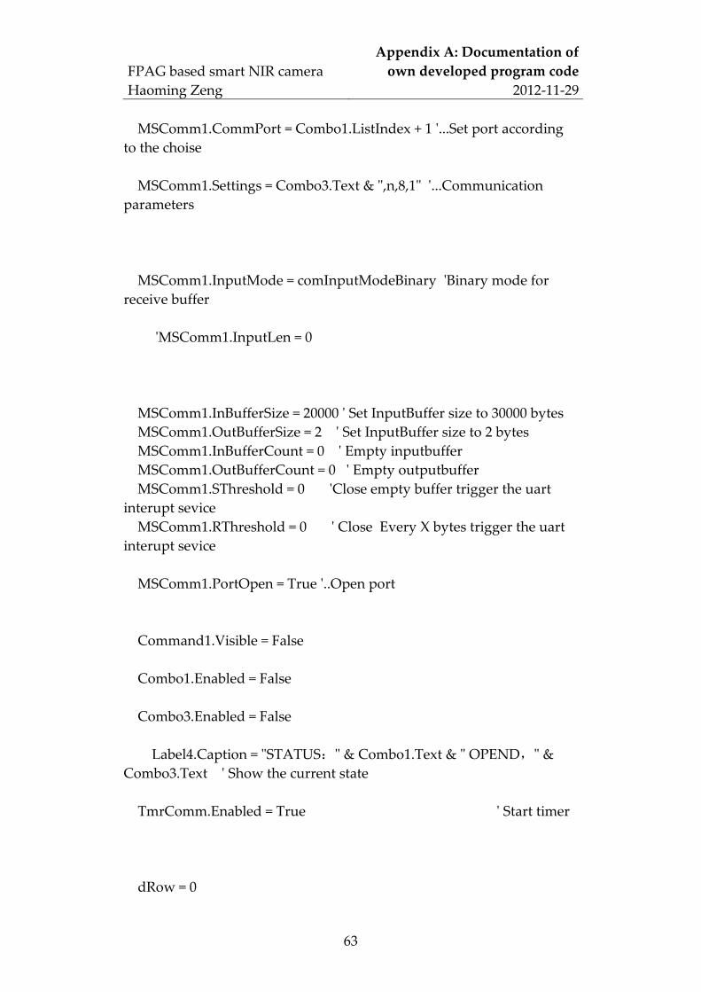
FPAG based smart NIR camera
Haoming Zeng
Appendix A: Documentation of
own developed program code
2012-11-29
63
MSComm1.CommPort = Combo1.ListIndex + 1 '...Set port according
to the choise
MSComm1.Settings = Combo3.Text & ",n,8,1" '...Communication
parameters
MSComm1.InputMode = comInputModeBinary 'Binary mode for
receive buffer
'MSComm1.InputLen = 0
MSComm1.InBufferSize = 20000 ' Set InputBuffer size to 30000 bytes
MSComm1.OutBufferSize = 2 ' Set InputBuffer size to 2 bytes
MSComm1.InBufferCount = 0 ' Empty inputbuffer
MSComm1.OutBufferCount = 0 ' Empty outputbuffer
MSComm1.SThreshold = 0 'Close empty buffer trigger the uart
interupt sevice
MSComm1.RThreshold = 0 ' Close Every X bytes trigger the uart
interupt sevice
MSComm1.PortOpen = True '..Open port
Command1.Visible = False
Combo1.Enabled = False
Combo3.Enabled = False
Label4.Caption = "STATUS:" & Combo1.Text & " OPEND," &
Combo3.Text ' Show the current state
TmrComm.Enabled = True ' Start timer
dRow = 0
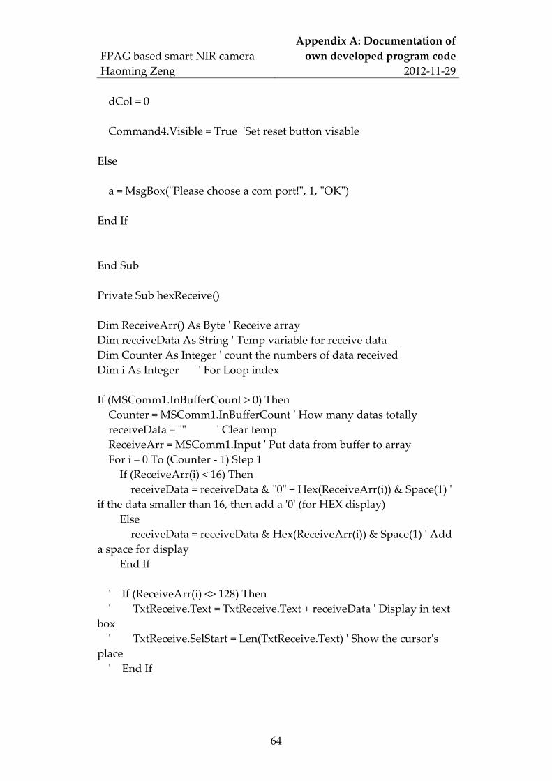
FPAG based smart NIR camera
Haoming Zeng
Appendix A: Documentation of
own developed program code
2012-11-29
64
dCol = 0
Command4.Visible = True 'Set reset button visable
Else
a = MsgBox("Please choose a com port!", 1, "OK")
End If
End Sub
Private Sub hexReceive()
Dim ReceiveArr() As Byte ' Receive array
Dim receiveData As String ' Temp variable for receive data
Dim Counter As Integer ' count the numbers of data received
Dim i As Integer ' For Loop index
If (MSComm1.InBufferCount > 0) Then
Counter = MSComm1.InBufferCount ' How many datas totally
receiveData = "" ' Clear temp
ReceiveArr = MSComm1.Input ' Put data from buffer to array
For i = 0 To (Counter - 1) Step 1
If (ReceiveArr(i) < 16) Then
receiveData = receiveData & "0" + Hex(ReceiveArr(i)) & Space(1) '
if the data smaller than 16, then add a '0' (for HEX display)
Else
receiveData = receiveData & Hex(ReceiveArr(i)) & Space(1) ' Add
a space for display
End If
' If (ReceiveArr(i) <> 128) Then
' TxtReceive.Text = TxtReceive.Text + receiveData ' Display in text
box
' TxtReceive.SelStart = Len(TxtReceive.Text) ' Show the cursor's
place
' End If

FPAG based smart NIR camera
Haoming Zeng
Appendix A: Documentation of
own developed program code
2012-11-29
65
Picture1.PSet (dCol, dRow), RGB(CInt(ReceiveArr(i)),
CInt(ReceiveArr(i)), CInt(ReceiveArr(i))) 'Draw pixel
'Picture1.PSet (dRow, dCol), CInt(ReceiveArr(i)) 'Draw pixel
dCol = dCol + 1
If dCol = imgWidth Then
dCol = 0
dRow = dRow + 1
If dRow = imgHeight Then
dRow = 0
SavePicture Picture1.Image, "c:\NIR" & CStr(Index) & ".bmp"
'Save into bmp file
Index = Index + 1
End If
End If
Next i
TxtReceive.Text = TxtReceive.Text + receiveData ' Display in text box
TxtReceive.SelStart = Len(TxtReceive.Text) ' Show the cursor's place
End If
''''''''''''''''''''''''''''''''''''''''''''''''''''''''''
'This counter will lead to software crash
'if the PC in bad condition (such as too much software running at the
same time)
''''''''''''''''''''''''''''''''''''''''''''''''''''''''''
ReceiveCount = ReceiveCount + Counter ' Count how many datas
received in total
If ReceiveCount > 10000 Then 'Due to one integer can not display a
value which out of range
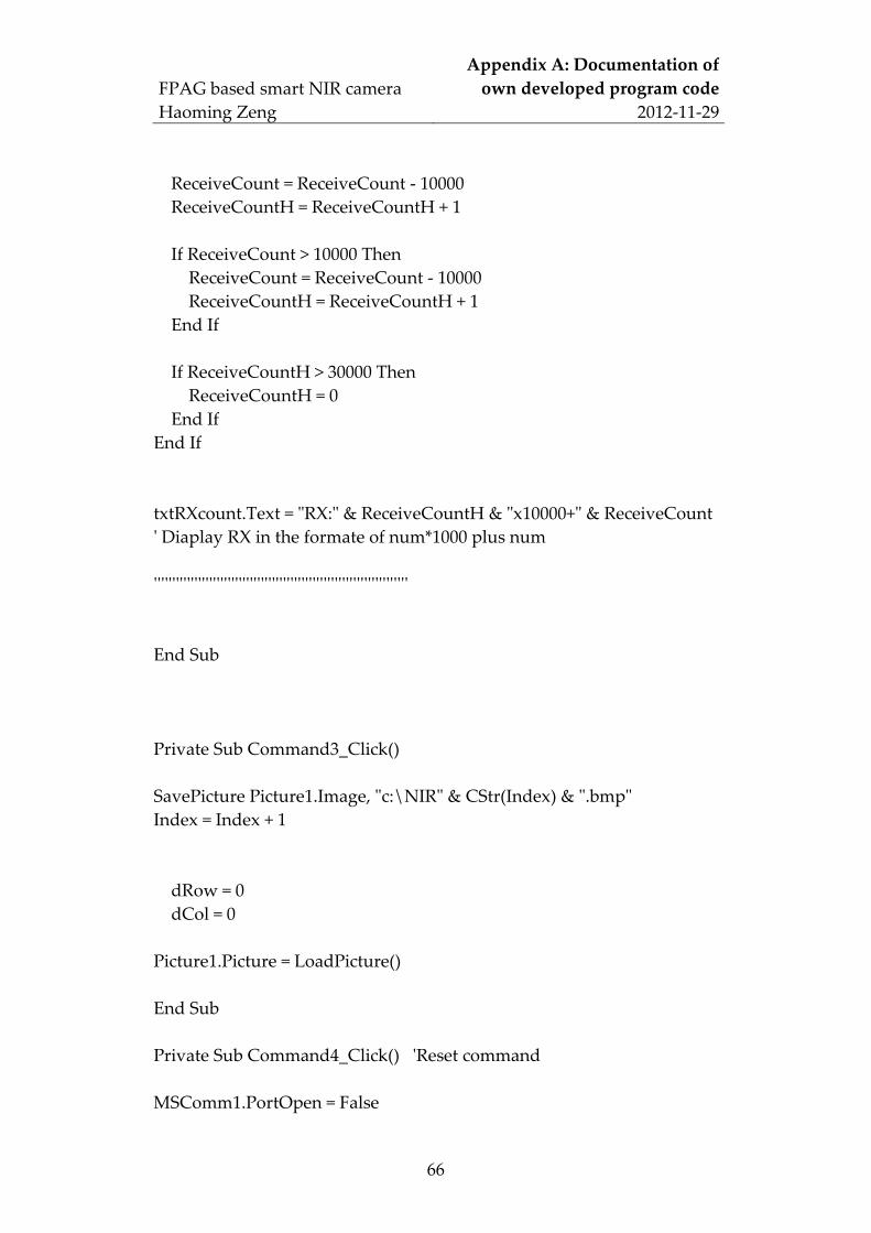
FPAG based smart NIR camera
Haoming Zeng
Appendix A: Documentation of
own developed program code
2012-11-29
66
ReceiveCount = ReceiveCount - 10000
ReceiveCountH = ReceiveCountH + 1
If ReceiveCount > 10000 Then
ReceiveCount = ReceiveCount - 10000
ReceiveCountH = ReceiveCountH + 1
End If
If ReceiveCountH > 30000 Then
ReceiveCountH = 0
End If
End If
txtRXcount.Text = "RX:" & ReceiveCountH & "x10000+" & ReceiveCount
' Diaplay RX in the formate of num*1000 plus num
'''''''''''''''''''''''''''''''''''''''''''''''''''''''''''''''''''''
End Sub
Private Sub Command3_Click()
SavePicture Picture1.Image, "c:\NIR" & CStr(Index) & ".bmp"
Index = Index + 1
dRow = 0
dCol = 0
Picture1.Picture = LoadPicture()
End Sub
Private Sub Command4_Click() 'Reset command
MSComm1.PortOpen = False
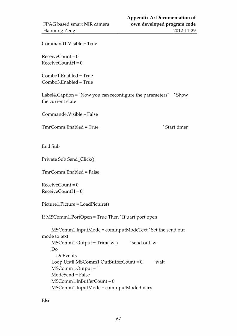
FPAG based smart NIR camera
Haoming Zeng
Appendix A: Documentation of
own developed program code
2012-11-29
67
Command1.Visible = True
ReceiveCount = 0
ReceiveCountH = 0
Combo1.Enabled = True
Combo3.Enabled = True
Label4.Caption = "Now you can reconfigure the parameters" ' Show
the current state
Command4.Visible = False
TmrComm.Enabled = True ' Start timer
End Sub
Private Sub Send_Click()
TmrComm.Enabled = False
ReceiveCount = 0
ReceiveCountH = 0
Picture1.Picture = LoadPicture()
If MSComm1.PortOpen = True Then ' If uart port open
MSComm1.InputMode = comInputModeText ' Set the send out
mode to text
MSComm1.Output = Trim("w") ' send out 'w'
Do
DoEvents
Loop Until MSComm1.OutBufferCount = 0 'wait
MSComm1.Output = ""
ModeSend = False
MSComm1.InBufferCount = 0
MSComm1.InputMode = comInputModeBinary
Else

FPAG based smart NIR camera
Haoming Zeng
Appendix A: Documentation of
own developed program code
2012-11-29
68
MsgBox "Port is closed,please open it", 48, "NIR Pro" ' Warnning for
Port not open
End If
TmrComm.Enabled = True
End Sub
Private Sub TmrComm_Timer() 'Every preset time arriving (Set the
interval parameter of Timmer)
Dim Rx_buff() As Byte
Dim okstring As String
Dim ReceivedLen As Integer
TmrComm.Enabled = False 'Close timmer
If MSComm1.InBufferCount > 0 Then 'Check receive buffer
Call hexReceive
End If
TmrComm.Enabled = True 'Open timmer
End Sub
Private Sub Command2_Click() ' For QUIT
'...Quit
Unload Me
End Sub
Private Sub Form_Load() ' When the form is loaded
Combo1.AddItem "COM1"
Combo1.AddItem "COM2"
Combo1.AddItem "COM3"
Combo1.AddItem "COM4"
Combo1.AddItem "COM5"
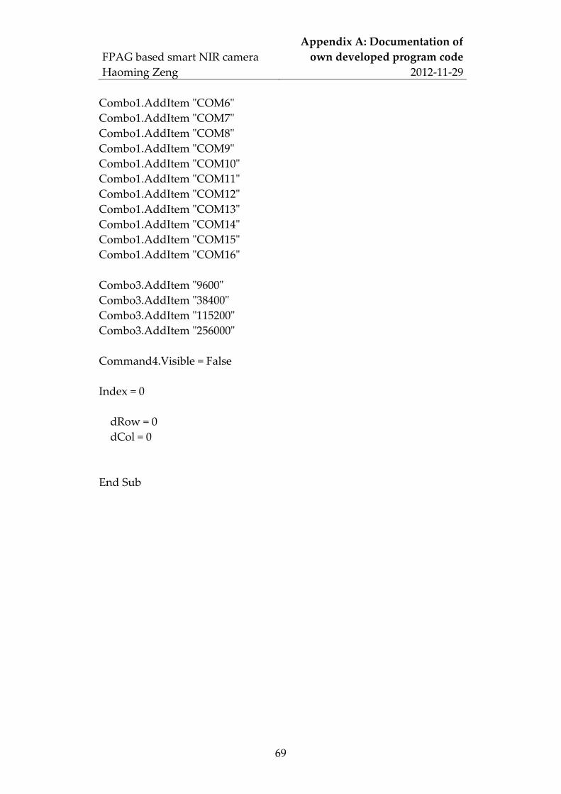
FPAG based smart NIR camera
Haoming Zeng
Appendix A: Documentation of
own developed program code
2012-11-29
69
Combo1.AddItem "COM6"
Combo1.AddItem "COM7"
Combo1.AddItem "COM8"
Combo1.AddItem "COM9"
Combo1.AddItem "COM10"
Combo1.AddItem "COM11"
Combo1.AddItem "COM12"
Combo1.AddItem "COM13"
Combo1.AddItem "COM14"
Combo1.AddItem "COM15"
Combo1.AddItem "COM16"
Combo3.AddItem "9600"
Combo3.AddItem "38400"
Combo3.AddItem "115200"
Combo3.AddItem "256000"
Command4.Visible = False
Index = 0
dRow = 0
dCol = 0
End Sub