Development of a CMOS pixel sensor with on-chip artificial ...
174
HAL Id: tel-02517257 https://tel.archives-ouvertes.fr/tel-02517257 Submitted on 24 Mar 2020 HAL is a multi-disciplinary open access archive for the deposit and dissemination of sci- entific research documents, whether they are pub- lished or not. The documents may come from teaching and research institutions in France or abroad, or from public or private research centers. L’archive ouverte pluridisciplinaire HAL, est destinée au dépôt et à la diffusion de documents scientifiques de niveau recherche, publiés ou non, émanant des établissements d’enseignement et de recherche français ou étrangers, des laboratoires publics ou privés. Development of a CMOS pixel sensor with on-chip artificial neural networks Ruiguang Zhao To cite this version: Ruiguang Zhao. Development of a CMOS pixel sensor with on-chip artificial neural networks. High En- ergy Physics - Experiment [hep-ex]. Université de Strasbourg, 2019. English. NNT : 2019STRAE050. tel-02517257
Transcript of Development of a CMOS pixel sensor with on-chip artificial ...

HAL Id: tel-02517257https://tel.archives-ouvertes.fr/tel-02517257
Submitted on 24 Mar 2020
HAL is a multi-disciplinary open accessarchive for the deposit and dissemination of sci-entific research documents, whether they are pub-lished or not. The documents may come fromteaching and research institutions in France orabroad, or from public or private research centers.
L’archive ouverte pluridisciplinaire HAL, estdestinée au dépôt et à la diffusion de documentsscientifiques de niveau recherche, publiés ou non,émanant des établissements d’enseignement et derecherche français ou étrangers, des laboratoirespublics ou privés.
Development of a CMOS pixel sensor with on-chipartificial neural networks
Ruiguang Zhao
To cite this version:Ruiguang Zhao. Development of a CMOS pixel sensor with on-chip artificial neural networks. High En-ergy Physics - Experiment [hep-ex]. Université de Strasbourg, 2019. English. �NNT : 2019STRAE050�.�tel-02517257�

UNIVERSITÉ DE STRASBOURG Logo Ecole
doctorale
ÉCOLE DOCTORALE Physique et Chimie-Physique
Institut pluridisciplinaire Hubert Curien (IPHC) - UMR 7178
THÈSE présentée par :
Ruiguang ZHAO
soutenue le : 20 Décembre 2019
pour obtenir le grade de : Docteur de l’université de Strasbourg
Discipline/ Spécialité : Électronique, Microélectronique, Photonique
Development of a CMOS pixel sensor with on-chip artificial neural networks
THÈSE dirigée par :
M. HU Yann Professeur, Université de Strasbourg RAPPORTEURS :
M. DE LA TAILLE Christophe Directeur, Laboratoire OMEGA M. BERRY François Professeur, Institut PASCAL
AUTRES MEMBRES DU JURY : M. PRIGENT Michel Professeur, Institut XLIM Mme. COURTIN Sandrine Professeur, Université de Strasbourg M. BESSON Auguste Maître de Conférences, Université de Strasbourg


I
Contents
!
Contents ................................................................................................................. I
Acknowledgements .............................................................................................. V
List of Figures .................................................................................................... VII
List of Tables ....................................................................................................... XI
Résumé en Français ........................................................................................ XIII
Introduction .................................................................................................. XXIII
1 International Linear Collider ....................................................................... 1
1.1 ILC Project ............................................................................................... 1
1.1.1 Physics Programs of the ILC ............................................................ 2
1.1.2 ILC Layout ....................................................................................... 4
1.2 ILC Experimental Conditions .................................................................. 5
1.2.1 Beam Structure ................................................................................. 5
1.2.2 Beam Background ............................................................................ 5
1.3 International Large Detector .................................................................... 6
1.3.1 Vertex Detector ................................................................................. 7
1.3.2 Silicon Tracking Part ...................................................................... 11
1.3.3 Time Projection Chamber ............................................................... 11
1.3.4 Calorimeter System ........................................................................ 12
1.3.5 Muon System .................................................................................. 12
1.3.6 Coil and Yoke System ..................................................................... 12
1.4 Motivation .............................................................................................. 12

Contents
II
1.4.1 Challenges for Track Reconstruction ............................................. 12
1.4.2 Trajectory of Charged Particles ...................................................... 14
1.4.3 Principle for Particle Recognition .................................................. 17
1.5 Summary ................................................................................................ 18
1.6 Bibliography .......................................................................................... 19
2 Semiconductor Detectors ............................................................................ 23
2.1 Carriers Generation ................................................................................ 24
2.1.1 Carriers Generated by Photons ....................................................... 24
2.1.2 Carriers Generation by Charged Particles ...................................... 25
2.2 Carriers Transport .................................................................................. 26
2.2.1 Drift ................................................................................................ 26
2.2.2 Diffusion ......................................................................................... 26
2.3 P-N Junction........................................................................................... 27
2.3.1 Forward Bias................................................................................... 28
2.3.2 Reverse Bias ................................................................................... 28
2.4 Metal-Oxide-Semiconductor .................................................................. 29
2.5 Silicon Detector Types ........................................................................... 30
2.5.1 Strip Detector .................................................................................. 30
2.5.2 CCD ................................................................................................ 32
2.5.3 Hybrid Pixel Sensor ........................................................................ 33
2.5.4 DEPFET Sensor .............................................................................. 34
2.5.5 Monolithic Active Pixel Sensor ...................................................... 34
2.5.6 Conclusions .................................................................................... 36
2.6 Summary ................................................................................................ 38
2.7 Bibliography .......................................................................................... 39
3 Artificial Neural Networks for Pattern Recognition ................................ 43
3.1 Pattern Recognition ................................................................................ 43
3.2 Biological and Artificial Neuron ............................................................ 45
3.2.1 Biological Neurons ......................................................................... 45
3.2.2 Artificial Neuron ............................................................................. 46
3.2.3 Activation Function ........................................................................ 47
3.3 Types of Artificial Neural Networks ...................................................... 49
3.3.1 Multi-Layer Perceptron (MLP) ...................................................... 50
3.4 Feature Extraction .................................................................................. 51

Contents
III
3.5 ANN Supervised Learning ..................................................................... 52
3.5.1 BP Algorithm .................................................................................. 53
3.6 ANN in HEP .......................................................................................... 57
3.7 Challenges for ANN Implementation .................................................... 59
3.8 Summary ................................................................................................ 60
3.9 Bibliography .......................................................................................... 61
4 FPGA Implementation of ANN for Reconstructing Incident Angles ..... 65
4.1 Raw Data Acquisition System ............................................................... 66
4.1.1 CMOS Pixel Sensor ........................................................................ 67
4.1.2 2 Rotations Support ........................................................................ 68
4.1.3 Readout Chain ................................................................................ 73
4.2 Implementations in the FPGA ............................................................... 74
4.2.1 Interface to Read in Raw Data ........................................................ 76
4.2.2 Cluster Search ................................................................................. 79
4.2.3 Data Format Conversion ................................................................. 86
4.2.4 Feature Extraction ........................................................................... 87
4.2.5 Normalized Features ....................................................................... 93
4.2.6 ANN Implementation ..................................................................... 93
4.2.7 DeNormalized Module ................................................................... 96
4.2.8 Interface to Output .......................................................................... 97
4.3 Test results ............................................................................................. 99
4.3.1 Analysis and Discussion ............................................................... 100
4.4 Summary .............................................................................................. 102
4.5 Bibliography ........................................................................................ 103
5 An On-chip Algorithm for Cluster Search .............................................. 105
5.1 Motivation ............................................................................................ 105
5.2 Algorithm for Cluster Search ............................................................... 106
5.2.1 Algorithm for One Column .......................................................... 107
5.2.2 Steps for a Cluster......................................................................... 110
5.2.3 Supplementary Explanation .......................................................... 112
5.3 Simulation Results ............................................................................... 115
5.3.1 Cluster Windows ........................................................................... 115
5.3.2 Seed Thresholds ............................................................................ 117
5.3.3 Algorithm in the FPGA VS. Algorithm Proposed ........................ 118

Contents
IV
5.4 Discussion ............................................................................................ 120
5.4.1 Large Clusters ............................................................................... 120
5.4.2 Separated Parts ............................................................................. 122
5.4.3 Overlap Parts ................................................................................ 123
5.5 Algorithm Implementation................................................................... 124
5.5.1 Implementation of the 64-column Algorithm ............................... 124
5.5.2 Timing ........................................................................................... 127
5.5.3 Simulation of the 256-column Implementation ............................ 129
5.5.4 Synthesized Result of the 64-column Implementation ................. 130
5.6 Summary .............................................................................................. 132
5.7 Bibliography ........................................................................................ 133
6 Conclusions and Perspectives ................................................................... 135

V
Acknowledgements
I would like to thank China Scholarship Council (CSC) for the financial support
during my doctoral study at University of Strasbourg France and Institut
Pluridisciplinaire Hubert Curien (IPHC), CNRS.
This thesis was made possible by the support of many individuals during my past
four years in France. I would like to express my sincere gratitude to my supervisor Prof.
Yann HU and Marc WINTER, the leader of the CMOS-ILC research group, for
offering me the opportunity to work in IPHC. Their guidance has been helpful during
my research and for writing this thesis. I sincerely appreciate Dr. Auguste BESSON for
his guidance and fruitful suggestions throughout my doctoral study, the analysis of the
simulation result, and providing the corrections and suggestions for this thesis.
I am grateful to Dr. Christine HU-GUO, the director of the microelectronic group,
for giving me insightful guidance for my design and providing exhaustive suggestions
for my publications and posters.
I would like to thank Prof. Michel PAINDAVOINE, in Electronics, Signal and
Image Processing of Burgundy University, for communication and guidance at the
beginning of my thesis. I would like to thank Luis alejandro PEREZ PEREZ and
Mathieu GOFFE for their help in the whole process of the raw data acquisition and the
ANN training. I am grateful to Kimmo JAASKELAINEN for his help in the FPGA
system design. I would like to thank Claude COLLEDANI and Guy DOZIERE for
providing help and offering encouragements during my doctoral period.
I would also like to thank all my colleagues in IPHC: Jerome BAUDOT, Frederic
MOREL, Abdelkader HIMMI, Gregory BERTOLONE, Isabelle VALIN, Maciej
KACHEL, Gilles CLAUS, Mathieu SPECHT, Christian ILLINGER, Andrei

Acknowledgements
VI
DOROKHOV, Pham Thanh HUNG and Yu ZHANG for their kind help and technical
support in my work.
I would like to express my respect to doctoral candidates, Julian HEYMES and Yue
ZHAO, of our group. We got together to share ideas, discussed processes and analysed
results.
I am so appreciated to my friends Jiahui FAN, Siyu LU who gave me faithful
supports during the whole stage of my thesis.
Last but not least, I would like to thank my parents for raising me and making me
be surrounded by unconditional support, understanding and love. I am very grateful to
my future girlfriend, thanks for her absence during my doctoral period and did not hurt
my heart.

VII
List of Figures
Figure 1: International Grand Detector (ILD) et Silicon Detector (SiD). ........................... XIV
Figure 2: Les formes de cluster générées par des particules du processus physique VS.
l'arrière-plan de faisceau. ........................................................................................................ XV
Figure 3: L'ANN implémentée dans le FPGA. .................................................................... XVI
Figure 4: . Le résultat du test de 500 trames de données brutes dans chaque angle d'incidence
donné. .................................................................................................................................. XVII
Figure 5: La description de la procédure de l'algorithme. ................................................... XIX
Figure 6: Structure de l'algorithme implémenté dans une matrice à 64 colonnes. ................ XX
Figure 1.1: Schematic layout of the ILC in the 250 GeV staged configuration [18]. ............... 4
Figure 1.2: Beam structure of the ILC. ..................................................................................... 5
Figure 1.3: Illustration of the pinch effect and generation of beamstrahlung photons in bunch
collisions. ................................................................................................................................... 6
Figure 1.4: Two detectors and the "push-pull" mode [25]. ....................................................... 7
Figure 1.5: Quadrant view of the ILD detector concept. Dimensions are in mm [26]. ............ 7
Figure 1.6: Impact parameter resolution (a) Finite single point resolution (b) Multiple
scattering. .................................................................................................................................. 8
Figure 1.7: Impact parameter resolution as a function of the particle momentum. .................. 9
Figure 1.8: Vertex detector scheme of the ILD. ..................................................................... 10
Figure 1.9: ILD schemes of the silicon tracking system. ........................................................ 11
Figure 1.10: Beam background features simulation [29]. ...................................................... 13
Figure 1.11: Schematic diagram of tracks generated by particles, one is created by a particle
with high momentum (blue) and others are created by particles with low momenta. ............. 13
Figure 1.12: Helix trajectory of charged particles under the effect of the magnetic field. ..... 14
Figure 1.13: Trajectory projection of a charged particle on the transverse plane. .................. 14
Figure 1.14: Incident angle θT as a function of the particle transverse momentum (PT). ....... 16
Figure 1.15: Trajectory projection of a charged particle on the parallel plane. ...................... 17
Figure 1.16: Schematic diagram of an incident angle on the vertex detector. ........................ 17
Figure 1.17: Cluster shapes generated by particles from the physics process and particles from
the beam background. .............................................................................................................. 18

List of Figures
VIII
Figure 2.1: Typical semiconductor detector system. .............................................................. 23
Figure 2.2: Generation of electrons and holes by absorption of photons, the energy loss=
Eg, >Eg, and < Eg [5]. ............................................................................................................. 25
Figure 2.3: P-N junction (a) Depletion region (b) Energy band diagram. .............................. 27
Figure 2.4: P-N junction under forward bias (a) Depletion region (b) Energy band diagram.28
Figure 2.5: P-N junction under reverse bias (a) Depletion region (b) Energy band diagram. 28
Figure 2.6: N-type Metal-Oxide-Semiconductor structure. .................................................... 29
Figure 2.7: An n-type MOS under accumulation, depletion and inversion conditions [10]. .. 29
Figure 2.8: Single-sided strip detector (a) DC coupled strip detector (b) AC coupled strip
detector [13]. ........................................................................................................................... 31
Figure 2.9: Operation principle of a double-sided strip detector [17]. ................................... 32
Figure 2.10: Timing diagram of voltage schemes to transport charge through a three-phase
CCD. ........................................................................................................................................ 32
Figure 2.11: A simplified schematic diagram of a single pixel in a hybrid silicon detector, it is
composed of a sensor part and a readout electronics part [24]. ............................................... 33
Figure 2.12: Schematic layout of the DEPFET [27]. ............................................................. 34
Figure 2.13: Schematic of the first-generation MAPS structure. ........................................... 35
Figure 2.14: Schematic of the second-generation MAPS structure. ....................................... 35
Figure 2.15: Typical in-pixel readout circuit [30]. ................................................................. 36
Figure 3.1: Examples of cluster shapes (a) Cluster shape generated by charged particles from
the physics event (b) Cluster shape generated by charged a charged particle from the beam
background. ............................................................................................................................. 44
Figure 3.2: Connections between two biological neurons. ..................................................... 45
Figure 3.3: Computational model of artificial neurons. ......................................................... 46
Figure 3.4: McCulloch-Pitts model of an artificial neuron. ................................................... 47
Figure 3.5: Sigmoid activation functions. .............................................................................. 48
Figure 3.6: Taxonomy of feedforward and feedback network architectures [13]. ................. 49
Figure 3.7: Connection architectures of Multi-Layer Perceptron. .......................................... 50
Figure 3.8: Training and test phase [25]. ................................................................................ 52
Figure 3.9: Signal-flow graph of output neuron j. .................................................................. 55
Figure 3.10: Signal-flow graph of hidden neuron j. ............................................................... 56
Figure 3.11: Basic coincidence electric circuit. ...................................................................... 58
Figure 4.1: Main procedures of the offline methodology. The training and the test process in
TMVA have been accomplished by my colleague Luis alejandro PEREZ PEREZ .............. 65
Figure 4.2: Schematic diagram of the raw data acquisition system. ...................................... 66
Figure 4.3: CMOS pixel sensor MIMOSA 18 (a) Layout of MIMOSA 18 (b) The pixel
structure of the MIMOSA18 [3]. ............................................................................................. 67
Figure 4.4: Schematic of the 2 rotations support. ................................................................... 68
Figure 4.5: Simulation result of the correlation between incident angle φ, θ and α, β. .......... 72
Figure 4.6: Schematic diagram of the MIMOSA 18 readout chain [4]. ................................. 73
Figure 4.7: FPGA development board (Nexys Video Artix-7 FPGA) used in our study. ....... 74
Figure 4.8: Main procedures and timing in the FPGA device. ............................................... 75

List of Figures
IX
Figure 4.9: Frame format stored in a binary file (256×256 pixels). ....................................... 77
Figure 4.10: Timing waveform to read in raw data of an example from PC to the FPGA device.
................................................................................................................................................. 79
Figure 4.11: Incident angles of charged particles. .................................................................. 80
Figure 4.12: Algorithm for cluster search implemented in the FPGA device. ....................... 81
Figure 4.13: Steps of searching neighbour pixels around seed pixel. .................................... 82
Figure 4.14: Cluster counts found by algorithms with different cluster windows. ................ 84
Figure 4.15: Cluster counts of an elongated cluster found by the three algorithms. .............. 85
Figure 4.16: Simulation of cluster counts and effective surface. ........................................... 85
Figure 4.17: Format of Single-precision floating-point [10]. ................................................. 86
Figure 4.18: Stopping power for positive muons in cupper Straggling functions in silicon for
500MeV pions, normalized to unity at the most probable value Δp/x [12]. ............................ 88
Figure 4.19: The main axis of a cluster. ................................................................................. 88
Figure 4.20: Position of a fired pixel in a cluster. .................................................................. 90
Figure 4.21: Correlation between two coordinate systems. .................................................... 91
Figure 4.22: Structure of the artificial neural network. .......................................................... 93
Figure 4.23: Digital circuit of the artificial neural network. .................................................. 95
Figure 4.24: Reconstructed information format of a cluster. .................................................. 97
Figure 4.25: Timing of transporting the output result of one memory cell. ........................... 98
Figure 4.26: Reconstructed results of a frame of raw data (a) The content of reconstructed
results (b) First cluster shape (c) Second cluster shape. .......................................................... 99
Figure 4.27: Difference between the mean value of reconstructed angles and the incident angle.
............................................................................................................................................... 100
Figure 4.28: Distribution of reconstructed angles θrec versus incident angles θinc. ............... 101
Figure 5.1: Definition of a seed pixel in a cluster. ................................................................ 107
Figure 5.2: Flowchart of the algorithm proposed. ................................................................ 108
Figure 5.3: Comparison between the data [3] and the max_value register. .......................... 109
Figure 5.4: Comparison between the column seed pixel and the neighbour max_value registers.
............................................................................................................................................... 109
Figure 5.5: Information of an example cluster. ..................................................................... 110
Figure 5.6: Processing steps of the example cluster. ............................................................. 111
Figure 5.7: Two "seed pixels" in the same column, pixel A is the seed pixel, pixel B is a part of
the cluster. ............................................................................................................................... 114
Figure 5.8: Two "seed pixels" in the same row, pixel A is the seed pixel, pixel B is a part of the
cluster...................................................................................................................................... 114
Figure 5.9: Simulation results of cluster counts found by algorithms proposed in this chapter
with different cluster windows (7×7 and 5×5 cluster window). ............................................. 116
Figure 5.10: Simulation results of the percentage of lost cluster counts between algorithms
with the 7×7 and the 5×5 cluster window. .............................................................................. 117
Figure 5.11: Simulation results of cluster counts by algorithms with different seed thresholds.
................................................................................................................................................ 118
Figure 5.12: Simulation results of cluster counts found by the algorithm proposed VS.

List of Figures
X
implemented in the FPGA device. .......................................................................................... 119
Figure 5.13: Example of a large cluster in a matrix of 7×9 pixels. ...................................... 121
Figure 5.14: Example of separated parts in a matrix of 7×7 pixels. ..................................... 122
Figure 5.15: Example of overlap parts in a matrix of 8×7 pixels. ........................................ 123
Figure 5.16: Schematic of the algorithm implemented in 64 columns. ................................ 125
Figure 5.17: Implementation of the cluster search unit. ....................................................... 126
Figure 5.18: Timing of generating two seed pixels at one row. ............................................ 128
Figure 5.19: Simulation of cluster counts found by the algorithm with different modules. . 129
Figure 5.20: Schematic of MCA and ANN modules implemented for modules of the
32-column matrix. ................................................................................................................. 131
Figure 6.1: Schematic diagram of a seed pixel in a 3×3 cluster window. A cluster is composed
of one seed pixel (P0) and 4 fired pixels. Two possible seed pixels (P0 and P1) are compared
with their 8 neighbours in the 3×3 cluster window. Due to charge of P1 is fewer than P0, just
pixel P0 is defined as a seed pixel in the 3×3 cluster window. .............................................. 141
Figure 6.2: Schematic diagram of a seed pixel in a 5×5 cluster window. Charges of the 3 fired
pixels in the 3×3 cluster window are replaced by seed pixel charge. Processed by step 4, charges
of the fired pixels are larger than their neighbours, pixel P0 is extracted as the seed pixel in the
5×5 cluster window. .............................................................................................................. 141
Figure 6.3: Schematic structure of a pixel for cluster search. .............................................. 142
Figure 6.4: Steps of on-chip feature extraction. ................................................................... 142
Figure 6.5: Example of on-chip feature extraction. The convolution operation is processed
between the four operators and a cluster at a step of 2 pixels. Four submatrices are created and
presented in level 1. The convolution operation is processed again between the four operators
and these submatrices at a step of 1 pixel. 16 values are produced in level 2. Convolution
procedures of three values in submatrix in level 1 is shown. ................................................ 143

XI
List of Tables
Table 1-1: Major physics processes to be studied by the ILC [17]. .......................................... 3
Table 1-2: Parameter a and b for detectors. .............................................................................. 9
Table 1-3: Parameters of the design composed of three layers of double-sided ladders [26]. 10
Table 1-4: Minimum transverse momentum of a particle to arrive different layers (Rlayer is the
radius of the vertex detector and R is the radius of the particle trajectory). ............................ 15
Table 2-1: Advantages and disadvantages of these detector technologies [6]. ....................... 37
Table 4-1: The setting of the angle θ, φ, and α, β. .................................................................. 73
Table 5-1: Simulation results of the occupied surface and power consumption of the 64-column
implementation. ..................................................................................................................... 130

XIII
Résumé en Français
A. Introduction
Le modèle standard de la physique des particules est un cadre théorique utilisé pour
décrire les particules fondamentales constituant la matière ordinaire et les forces
fondamentales. Les expériences de physique des hautes énergies (HEP) sont conçues
pour rechercher des particules fondamentales via des collisions parmi une grande
quantité de particules de haute énergie. Divers détecteurs sont équipés autour du point
d’interaction pour détecter et enregistrer les informations relatives aux collisions.
L'ILC (International Linear Collider) est un projet d'accélérateur linéaire de particules
proposé pour les expériences HEP, en complément du LHC (Large Hadron Collider) au
CERN. En raison de leur courte durée de vie, de l'ordre de plusieurs picosecondes, les
quarks lourds doivent être reconnus par les trajectoires partant du vertex de la
décroissance secondaire. Le détecteur de vertex (VTX) sera situé près du point
d’interaction.
Dans les expériences HEP, différents types de détecteurs à semi-conducteurs ont
été utilisés pour la détection et la mesure de la position du passage des particules. Les
capteurs à pixels CMOS (CPS) également appelés capteurs monolithiques à pixels
actifs (MAPS) et proposés par des chercheurs de l'IPHC-Strasbourg (Institut
Pluridisciplinaire Hubert Curien), intègrent sur un même substrat l'électronique pour la
détection et la lecture des signaux. Les CPS constituent un condidali naturel pour
l'équipement du VTX, car ils offrent un très bon compromis entre la granularité, le
budget de matière, la tolérance au rayonnement et la vitesse de lecture. Ils ont été
utilisés pour la jouvence du détecteur PiXeL (PXL) de l'expérience STAR au RHIC et

Résumé en Français
XIV
sont actuellement en phase de production pour la mise à jour de l'ITS (Inner Tracking
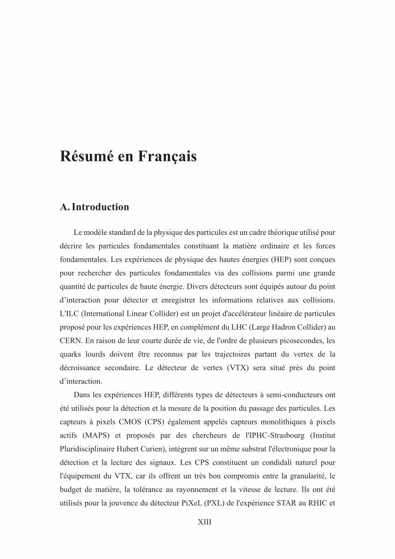
System) de l'expérience ALICE-LHC. Comme le montre la figure 1, Le point
d'interaction est entouré de deux détecteurs , (International Grand Detector (ILD) et
Silicon Detector (SiD)), qui fonctionnent selon un schéma push-pull pour partager la
même luminosité.
Figure 1: International Grand Detector (ILD) et Silicon Detector (SiD).
Dans le détecteur de vertex de l'ILC, la simulation Monte-Carlo montre qu'un
nombre élevé d'impacts supplémentaires seront générés par des électrons résultant de
processus liés au bruit de fond des faisceaux. Leur impulsion se trouve typiquement
dans la gamme de 10-100 MeV/c, et est généralement à celle des particules issues
d'événements associés à des processus physiques.
Sous l'effet du champ magnétique dans le détecteur, les électrons provenant du
bruit de fond, en raison de leur faible impulsion, traversent les détecteurs avec un grand
angle d'incidence par rapport à la normale au plan des détecteurs. Les paires
électrons-trous, environ ~80 e-h/µm, sont créées par le processus d'ionisation lorsque
les particules chargées traversent la couche épitaxiale. Les électrons sont collectés par
la diode de collection implantée dans chaque pixel. Les amas de pixels (clusters)
générés par les électrons issus du bruit de fond présentent des formes plutôt allongés
comme le montre la figure 2. En considérant les réseaux neuronaux artificiels (ANNs)
qui ont été largement utilisés dans le domaine de la reconnaissance de motifs, notre
groupe à l'IPHC a proposé d'explorer le concept d'un capteur à pixels CMOS avec des
ANNs intégrés pour marquer et supprimer les pixels touchés (hits) générés par ces
électrons.

Résumé en Français
XV
Figure 2: Les formes de cluster générées par des particules du processus physique VS.
l'arrière-plan de faisceau.
Au cours de ma thèse de doctorat, je me suis concentré sur l'étude d'un capteur à
pixels CMOS avec des ANNs intégrés portant sur les aspects suivants :
I. L'implémentation de modules de prétraitement et d'un ANN dans un composant
FPGA pour l'étude de faisabilité ;
II. Un algorithme pour la recherche de clusters, qui fait partie des modules de
prétraitement, a été proposé en vue d'être intégré dans la conception de l'ASIC
(Application-Specific Integrated Circuit).
B. Travail Doctoral
1) L'implémentation dans un FPGA
Pour concevoir le capteur à pixels CMOS avec des réseaux neuronaux artificiels
intégrés, la première étape est l'étude de faisabilité qui consiste à comparer la mise en
œuvre de l'ANN dans le FPGA à celui mise en œuvre dans un software. Les deux
implémentations sont exploitées par une méthode offline, ce qui signifie que les
données brutes utilisées sont acquises par un système indépendant.
Le système d'acquisition de données brutes a été mis en place pour recueillir des
données brutes à partir d'un capteur existant, MIMOSA 18, illuminé par une source β⁻
de 90Sr. Un support à 2 rotations est utilisé pour placer le CPS. Dans le cas où la source
serait fixe, l'angle θ d'incidence des particules chargées peut être choisi en ajustant les
angles entre le support et le plan de référence.
Dans la procédure d'apprentissage effectuée par le logiciel appelé Toolkit for
Multivariate Data Analysis (TMVA), une grande quantité de données brutes a été
recueillie pour chaque angle θ d'incidence donné (10 au total) afin de former les poids
Résumé en Français
XVI
de l'ANN.
Pour l'implémentation de l'ANN dans le FPGA, j'ai déterminé d'abord les entrées
de l'ANN en utilisant des modules de prétraitement. Ensuite, j'ai implémenté ces
modules de prétraitement et l'ANN dans une carte de développement NEXYS VIDEO
FPGA en utilisant le langage de description matérielle. La procédure de test a été
accomplie dans le FPGA. 500 trames de données brutes ont été échantillonnées pour
chaque angle d'incidence donné afin de tester l'ANN. Les données brutes ont été
introduites dans le FPGA puis traitées par CDS (Correlated Double Sampling) et des
valeurs de pixel de 12 bits sont générées.
a. Modules de prétraitement
Les modules de prétraitement contiennent principalement la recherche de clusters
et l'extraction de paramètres. Le module de recherche de clusters est utilisé pour trouver
les pixels de départ et localiser les clusters dans la trame des valeurs de pixels. Les
modules d'extraction de fonctionnalités sont utilisés pour produire des paramètres
caractérisant un cluster. Quatre paramètres sont définis : la charge totale d'un cluster, la
charge d'un pixel de départ, les écarts-types maximum et minimum. Le module MCA
(Main Component Analysis) fait partie de l'extraction des fonctionnalités implémenté
dans le FPGA et est utilisé pour calculer les écarts-types maximum et minimum.
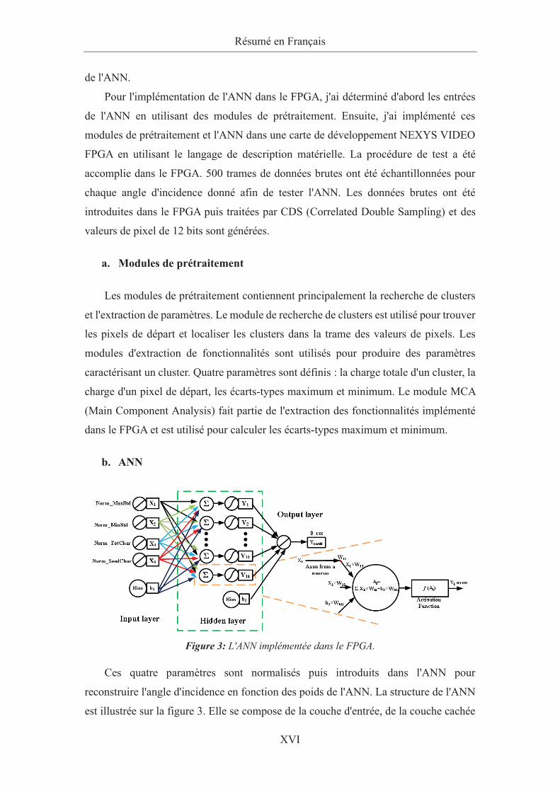
b. ANN
Figure 3: L'ANN implémentée dans le FPGA.
Ces quatre paramètres sont normalisés puis introduits dans l'ANN pour
reconstruire l'angle d'incidence en fonction des poids de l'ANN. La structure de l'ANN
est illustrée sur la figure 3. Elle se compose de la couche d'entrée, de la couche cachée

Résumé en Français
XVII
et de la couche de sortie. La couche d'entrée est composée de 4 neurones d'entrée et d'1
neurone de biais. La couche cachée qui vient après celle d'entrée a 14 neurones de
calcul et 1 neurone de biais. Le nombre de neurones de la couche cachée est déterminé
par la procédure d'apprentissage dans le software, en prenant en compte un équilibre
entre la complexité et les performances de la structure de l'ANN. La fonction
d'activation utilisée dans l'ANN est une tangente hyperbolique.
c. Résultats
(a). La distribution de l'angle reconstruit θrec
par le FPGA.
(b). La différence entre la valeur moyenne des
angles reconstitués ((((((((((((((((((((((((((((((((((((((((((((((((((((((((( ) et l'angle incident θinc.
Figure 4: . Le résultat du test de 500 trames de données brutes dans chaque angle d'incidence
donné.
Dans la procédure de test, j'ai enregistré et analysé les angles d'incidence
reconstruits. La figure 4(a) présente la distribution des angles reconstruits (θrec). Au
fure et à mesure que l'angle d'incidence (θinc) augmente, le pourcentage d'angles
reconstruits (θrec) entre 60 et 90 degrés augmente alors que le pourcentage d'angles
reconstruits (θrec) entre 30 et 50 degrés diminue. Compte tenu de l'application
spécifique du détecteur, la gamme d'angles reconstruits d'intérêt est comprise entre 50 à
75 degrés. Tout d'abord, les formes de clusters générées par des particules d'angles
d'incidence inférieurs à 50 degrés ne varient évidemment pas ou très peu. De plus, ces
angles d'incidence peuvent être directement reconstruites à partir des informations des
hits données par une échelle double-face (double-sided ladder). D'autre part, en raison
de la limitation de la fenêtre 7×7, les entrées ANN extraites des clusters présentent des
caractéristiques similaires si l'angle d'incidence est supérieur à 78 degrés.
La figure 4(b) représente la différence « D », voir dans la formule (1), entre la
valeur moyenne des angles reconstruits ( ) et l'angle d'incidence (θinc) ; notons que

Résumé en Français
XVIII
les résultats reconstruits par le FPGA sont présentés en rouge et ceux reconstruits par le
logiciel TMVA en bleu. On remarque que les angles reconstruits par les deux méthodes
ont la même valeur moyenne, ce qui valide l'étude de faisabilité. Cependant, ils ne
coïncident pas complètement en raison de la différence dans la précision des données
entre le hardware et le software.
De plus, les différences entre et θinc, que ce soient pour le FPGA ou pour le
TMVA, n'ont pas encore atteint un niveau de précision permettant de prédire l'angle
d'incidence réel car la structure de l'ANN et la procédure de formation doivent encore
être optimisées. Idéalement, la différence entre et l'angle d'incidence (θinc) devrait
se situer près de l'axe X (y=0).
Même si l’ANN n’a pas permis une reconstruction très précise, comme indiqué, les
résultats reconstruits présentent clairement la même tendance que la variété d'angles
d'incidence. En outre, la preuve du principe que les particules laissent une "signature"
qui dépend de l'angle d'incidence a été établie.
2) Un algorithme sur l'ASIC pour la recherche de cluster:
Le module de recherche de cluster implémenté dans le FPGA ne peut pas être
transplanté directement dans la conception ASIC. En premier lieu, un grand nombre de
mémoires serait nécessaire pour stocker une trame entière de valeurs de pixels; en
second lieu, beaucoup de ressource calcul et de temps seraient nécessaires pour détecter
les pixels voisins. J'ai proposé propose un algorithme pour la recherche de cluster qui
peut être intégré dans le capteur à pixels CMOS et collecter des clusters en temps réel.
a. Algorithm
Au lieu de rechercher des pixels de départ dans une matrice pixel par pixel,
l'algorithme recherche un pixel de départ en temps réel dans le processus de lecture de
la valeur de pixel ligne par ligne. Le pixel de départ est admis en comparant les pixels
situés au-dessus et en dessous de celui-ci et les pixels les plus grands situés dans les
colonnes gauche et droite d'une certaine plage de fenêtres. La procédure de l’algorithme
est illustrée à la figure 5.

Résumé en Français
XIX
Figure 5: La description de la procédure de l'algorithme.
b. Simulation
J'ai élaboré l'algorithme en code C et l'ai simulé. 500 trames de données brutes pour
chaque angle d'incidence donné sont utilisées pour tester ces algorithmes. Le résultat
montre que l'algorithme atteint le même niveau de comptage des clusters que les autres
algorithmes, y compris celui implémenté dans le FPGA.
c. Implémentation
La mise en oeuvre de l'algorithme est basée sur une matrice à modulo 2N-colonnes.
La figure 6 montre un exemple de deux modules de 32 colonnes (N=5). Les entrées de
l'implémentation sont les sorties des 64 ADC de colonne. Le niveau 1 se compose de 32
unités, chacune implémentant l'algorithme de recherche de cluster. Le niveau 2 a sept
(pour la fenêtre de 7×7) multiplexeurs 32-1. Le nombre de multiplexeurs est déterminé
par la taille de la fenêtre dans l'algorithme.

Résumé en Français
XX
Figure 6: Structure de l'algorithme implémenté dans une matrice à 64 colonnes.
J'ai implémenté la structure à 64 colonnes avec différents paramètres et effectué la
synthèse de ces implémentations en ciblant la technologie CMOS TowerJazz 0,18 µm.
Il n'y a pas de différence significative entre les implémentations dans une matrice à
modulo de 16 colonnes (N=4), 32-colonnes (N=5) et 64 colonnes (N=6) en termes de
surface occupée et de puissance dissipée. Toutefois, compte tenu de l'extraction des
fonctionnalités et du module ANN qui suivent la mise en œuvre de la recherche de
cluster, une surface occupée et une dissipation de puissances accrues sont nécessaires si
le modulo de 16 colonnes est utilisé. Ces deux paramètres d'évaluation peuvent être
diminués en utilisant la fenêtre de 5×5 au lieu de celle de 7×7. Ceux-ci pourraient
encore être améliorés avec une horloge à basse fréquence ou un ADC de basse
résolution. Si l'on choisit la technologie CMOS 65 nm, la densité d'intégration
augmente impliquant une diminution de la surface occupée et de la puissance
consommée. Si l'on utilise un substrat présentant une couche épitaxiale de haute
résistivité, une fenêtre de cluster plus petite peut alors être utilisée car les formes de
cluster générées par les particules sont réduites.
C. R&D
Sur la base des recherches de la thèse, le concept d'un capteur à pixels CMOS avec
des ANNs intégrés sera étudié plus avant en mettent l'accent sursous les deux aspects
suivants :
Optimiser l'ANN pour améliorer la précision de reconstruction:
L'architecture ANN doit être optimisée, telle que le nombre de neurones d'entrée.
Plusieurs fonctionnalités peuvent être introduites pour présenter un cluster. L'ANN
pourrait recevoir en entrée davantage de données brutes pour optimiser les poids afin

Résumé en Français
XXI
d'accroître la précision de la reconstruction.
Développer des modules fonctionnels sur puce pour réaliser la conception
matérielle complète
Une solution pour diminuer la dissipation de puissance de cette conception sera
d'optimiser le système de contrôle grâce à la technique dite de Power Gating qui permet
de couper l'alimentation des modules non utilisés. Pour la couche épitaxiale à haute
résistivité, la consommation d'énergie et les surfaces occupées du module seront
réduites grâce à l'application d'une petite fenêtre en clusters (5×5). En plus, un
algorithme sera proposé pour l'extraction des paramètres des clusters et intégré dans
l'ASIC.
Si la technologie CMOS 65 nm est utilisee à l'avenir, la surface occupée sera
réduite car une densité de circuit plus élevée est fournie; une réduction significative de
la consommation d'énergie pourra être obtenue en raison de la faible source de courant.
La technologie d'intégration 3D pourrait également être appliquée pour intégrer des
ANN dans le capteur àde pixels CMOS. La matrice de pixels et les modules de
traitement numérique (recherche de cluster, extraction de caractéristiques et ANN)
pourraient alors être séparés en différents niveaux.


XXIII
Introduction
High Energy Physics (HEP) experiments are established to extend and improve the
understanding of the universe. In machines of HEP experiments, physics particles are
accelerated and then taken into collisions. Various detectors equipped are used to record
and measure the products of the collisions. The International Linear Collider (ILC) as a
complementary experiment to the Large Hadron Collider (LHC) has been proposed.
The current program of the ILC for a 125 GeV Higgs boson will be processed at a
centre-of-mass energy of 250 GeV. The International Large Detector (ILD) and the
Silicon Detector(SiD) are two detector concepts that will be installed around the
interaction point and operated in a push-pull scheme to share the same luminosity.
Vertex detectors are located at the most inner part of a detector to measure the primary
interaction vertex and secondary vertices from decay particles under cooperation from
other tracking detectors. The vertex detector of the ILD consists of a cylindrical
concentric multi-layer structure to achieve an excellent spatial point resolution. On the
vertex detector, a large number of hits will be generated by electrons coming from the
beam background. These extra hits will increase the data flow and reduce the
bandwidth of the system. The momentum of these electrons coming from the beam
background typically lie in the range of 10-100 MeV/c, which is lower than that of
particles coming from physics events. Due to the effect of multiple scattering, the
reconstruction of tracks generated by low momentum particles is significantly
degraded.
In order to tag and remove the extra hits generated by background particles, this
thesis aims to make contributions to the development of a CMOS pixel sensor with
on-chip artificial neural networks.

Introduction
XXIV
Electron-hole pairs about ~80 e-h/µm are created by the ionization process when a
charged particle passes through the epitaxial layer of CMOS pixel sensors. Because of
diffusion, electrons generated are collected by two or more independent pixels that
constitute a charge cluster which expresses hit information. Under the effect of the
magnetic field in the detector, electrons from the beam background, owing to low
momenta, will cross the vertex detector with a large incident angle. Clusters generated
by these electrons (large incident angles) present rather elongated shapes.
CMOS pixel sensors (CPS), also named Monolithic Active Pixel Sensors (MAPS)
are monolithic devices that integrate signal sensing and readout electronics on the same
substrate. They offer an attractive balance among granularity, material budget, radiation
tolerance and readout speed. CMOS pixel sensors have been used in the PiXeL detector
(PXL) upgrade of the STAR experiment at RHIC and now are being built for the
upgrades of the Inner Tracking System (ITS) of the ALICE-LHC experiment.
Artificial Neural Networks (ANNs) are computational modules that are inspired by
the biological neural network. An ANN consists of processing units and connections
between these units. It has been proved that ANNs are suitable for pattern recognition
in a wide variety of field.
In this thesis, we study the feasibility of integrating ANNs within CPS to
reconstruct incident angles of particles. In addition, an algorithm for cluster search is
proposed to integrate into the CPS for real-time preprocessing.
The thesis is organized as follows,
· In chapter 1, ILC physics processes and layout are introduced briefly. Then,
major experimental conditions including beam structure and beam background
are presented. ILD, especially the vertex detector part, is presented. Finally,
due to challenges existing for multi-layer vertex detector targeting at low
momentum particles, the motivation of a CMOS pixel sensor with on-chip
artificial neural networks is provided. The trajectory of charged particles under
the effect of the magnetic field is projected on both the transverse and parallel
plane respectively and described.
· In chapter 2, the pinciple of carriers generation and transport in semiconductors
are introduced. Then, structures and bias modes of P-N junctions and
Metal-Oxide-Semiconductors are expressed. Lastly, several types of silicon
detectors are presented and compared.
· In chapter 3, pattern recognition is introduced firstly. The biological and

Introduction
XXV
artificial neuron structure and principle are explained. Then, a multi-layer
perceptron structure is presented. Next, the feature extraction procedure and
supervised learning procedure of ANN is outlined. ANN' applications in the
HEP are presented.
· In chapter 4, the feasibility study of the CMOS pixel sensor with on-chip ANNs,
which is achieved by the off-line method, is described in detail. Firstly, a raw
data acquisition system, including CMOS pixel sensor, 2 rotations support and
readout china is illustrated. Then, the entire design implemented in a Field
Programmable Gate Array (FPGA) development board is introduced in detail,
including the cluster search module, the feature extraction module and the
ANN structure. Lastly, the reconstruction results of incident angles by the ANN
are compared and analysed.
· In chapter 5, an on-chip algorithm for cluster search is proposed and presented.
Firstly, the motivation for the algorithm is given. Secondly, the algorithm is
illustrated in detail, including the principle description and detail step
demonstration. Then, simulation results are presented. Next, the discussion of
the algorithm is provided targeting at three cases of the cluster shape. Finally,
the implementation of the algorithm is expressed and the synthesized result of
the implementation is analysed.
· In conclusions, the results obtained in this thesis are summarized. In the end,
perspectives for the CPS integrated with ANNs are presented, including an
in-pixel algortihm for cluster search and an structure for feature extraction.


1
1 International Linear Collider
The ILC was proposed for the High Energy Physics (HEP) and encouraged by
requirements on the precision measurement of the Higgs Boson. The International
Linear Collider (ILC) is introduced briefly in the chapter, and the development
motivation of a CMOS Pixel Sensor (CPS) with on-chip Artificial Neural Networks
(ANNs) is also illustrated. Firstly, physics programs and the baseline of the ILC are
presented. Secondly, ILC experimental conditions and the International Large Detector
(ILD) are illustrated. The chapter ends with a description of the motivation for
developing a CMOS pixel sensor with on-chip ANNs, that is tagging and removing hits
generated by charged particles coming from the beam background based on the cluster
shapes.
1.1 ILC Project
Everything in the universe is found to be made from fundamental particles. A lot of
scientists are devoted to experimental and theoretical efforts, in order to explore the
nature of fundamental particles. The Standard Model (SM) is a theoretical framework,
which is proposed to explain the principle of fundamental particles constituents of
ordinary matter and related forces (including electromagnetic, weak, and strong
interactions, excepting the gravitational force). The current Standard Model was
finalized in the early 1970s, which has explained almost all results of HEP experiments
to date. For instance, the model has forecast the existence of quarks, the top quark, and
the tau neutrino and been confirmed. The Standard Model has become established as a

Chapter 1: International Linear Collider
2
well-tested physics theory [1][2].
HEP experiments are designed to research fundamental particles via collisions and
conversion among a large amount of high-energy particles. In machines, two beams of
particles are moved in opposite directions and accelerated, then brought into collisions
at the interaction point. Various detectors are equipped around the interaction point to
detect and record information of collisions [3][4].
In the past, a large number of high energy physics experiments and equipment have
been designed and established by physicists [5]. In 2012, a particle with a mass of about
125GeV was discovered by the ATLAS and CMS Collaborations at the Large Hadron
Collider (LHC) which is located at Geneva Switzerland [6]. Many properties of the
particle are in accordance with the postulated Higgs boson of the Standard Model.
Details of the Higgs boson and the presence or not of other anticipated new particles
need to be studied to complete the Standard Model framework. More precise
measurements of the Higgs boson can be achieved by lepton colliders which provide
the well-defined initial state of collisions and clean background level [7][8][9][10].
In 2001, a common conclusion was proposed by all three regional organizations
(ACFA in Asia, HEPAP in North America, and ECFA in Europe) of the HEP field: The
next major project in the HEP would be an electron-positron linear collider with a
centre-of-mass energy of 500 GeV named International Linear Collider [11][12]. In
autumn 2012, the Japanese high-energy physics community proposed to locate the ILC
in Japan. In 2013, after the discovery of the Higgs boson, the Technical Design Report
(TDR) for the ILC accelerator was published. The machine was designed to achieve a
centre–of–mass energy of 500 GeV [13][14].
According to the recommendation from the Japan Association of High Energy
Physicists (JAHEP) [15], the initial program of the ILC for a 125 GeV Higgs boson
would be started with a centre-of-mass energy of 250 GeV [7]. The ILC project is
divided into three phases, the preparation phase (2019/20-2022/2023), the construction
phase (foreseen from 2023) and the commissioning phase (foreseen 2031-2032) [16].
1.1.1 Physics Programs of the ILC
Major physics processes to be studied at various centre-of-mass energies (from 90
GeV to 1000 GeV) in the ILC are shown in table 1-1, Standard Model reactions and
physics goals are presented.

Chapter 1: International Linear Collider
3
Table 1-1: Major physics processes to be studied by the ILC [17].
Energy Reaction Physics goal
91 GeV e+e- → Z Ultra-precision electroweak
160 GeV e+e- → WW Ultra-precision W mass
250 GeV
(Current)
e+e- → Zh Precision Higgs couplings
350-400 GeV
(Upgrade)
e+e- → t t Top quark mass and couplings
e+e- → WW Precision W couplings
e+e- → v v h Precision Higgs couplings
500 GeV
(Upgrade)
e+e- → f f Precision search for Z’
e+e- → t t h Higgs coupling to top
e+e- → Zhh Higgs self-coupling
e+e- → x x Search for supersymmetry
e+e- → AH, H+H- Search for extended Higgs states
700-1000 GeV
(Upgrade)
e+e- → v v hh Higgs self-coupling
e+e- → v v VV Composite Higgs sector
e+e- → v v t t Composite Higgs and top
e+e- → t t * Search for supersymmetry
In the ILC, electrons and their antiparticles (positrons) are accelerated and collided
at high energy. The physics process of the ILC at a centre-of-mass energy of 250 GeV is
the reaction e+ e− → Zh. The current program of the ILC (250 GeV) will focus on
high-precision and model-independent measurements of the Higgs boson coupling. In
addition, it will search for direct new physics in exotic Higgs decays and in
pair-production of weakly interacting particles, even exploration of beyond the
Standard Model physics.
In the future, the ILC will be upgraded for raising the centre-of-mass energy to 500
GeV even 1 TeV. With the raising of the centre-of-mass energy, the ILC can be used to
take precision studies of the top quark and measurement of the top Yukawa coupling, to
determine the strength of the Higgs boson’s nonlinear self-interaction and to search for
new particles.

Chapter 1: International Linear Collider
4
1.1.2 ILC Layout
Figure 1.1: Schematic layout of the ILC in the 250 GeV staged configuration [18].
The schematic layout of the ILC in the current 250 GeV configuration is shown in
figure 1.1. It is composed of two linear accelerators that face each other, stretching
approximately 20.5 kilometres in length. Main parts of the ILC system are expressed as
[7]:
1. Electrons (e-) and Positrons (e+) Sources. They are designed to produce 5 GeV
beam pulses.
2. Damping Ring (DR). There are two oval DRs housing in a common tunnel,
operating at a beam energy of 5 GeV. Each oval DR has 3.2 km circumference.
They are used to accept electron and positron beams with large emittances and
produce the low-emittance beams, to dampen the incoming beam jitter to
provide highly stable beams and to delay bunches from the source.
3. Main Linac. Two main linacs are used to accelerate beams from 5 GeV to the
maximum 125 GeV. Each main linac is comprised of two parts. The first part is
a two-stage bunch compressor system. Beams are accelerated to 15 GeV in the
second stage and the bunch length is reduced from 6 mm to 0.33 mm. The
second part following the two-stage bunch compressor is the main linac which
is about 6 km.
4. Ring To Main Linac (RTML). It is the connection part between the DR and the
entrance of the main linac. It is used to transport of the beams from the DR to
upstream ends of the main linac, collimate the beam halo generated in the DR.
5. Beam Delivery System (BDS). Two BDSs are used to transport and focus
beams from two main linacs to the interaction point, then take beams into

Chapter 1: International Linear Collider
5
collisions. Each BDS is 2254 m long from the end of the main linac to the
interaction point.
1.2 ILC Experimental Conditions
Major experimental conditions of the ILC are introduced in the section, including
the beam structure and the beam background. Experimental conditions determine some
requirements for design of the detector.
1.2.1 Beam Structure
Figure 1.2: Beam structure of the ILC.
As presented in figure 1.2, the beam structure of the ILC is composed of trains at a
frequency of 5 Hz (5 trains/second). Each train maintains about 727 µs constituted by
1312 bunches. A bunch is separated from the other by ~554 ns. Between two trains
there is a period of ~199 ms named beamless time [7][13].
The beam structure is related to the design of detectors in the ILC. Average power
consumption of detectors can be reduced by switching off during beamless time which
occupies about 99% period. The known interval between every two bunches and trains
makes a possible to achieve detectors without triggers. The read-out strategy and
sequence are can be implemented between two bunches or after a train [19].
1.2.2 Beam Background
Beamstrahlung is the most important background in the ILC which is created via
the bunch interacting with the electromagnetic field of another bunch. In the approach
procedure of electron and positron bunches which have strong electric fields, as the

Chapter 1: International Linear Collider
6
small size of bunches indicates that they possess a very high space charge. As shown in
figure 1.3, under the effect of the electromagnetic field of bunches, two beams from
opposite directions do not point to each other directly, while towards the centre of the
oncoming bunch, which is named the pinch effect. Beamstrahlung photons are
generated by the beam-beam interaction to radiate the energy [20][21].
Electron-positron pairs with low momenta are released around the interaction point by
beamstrahlung photons, which makes a major contribution to the machine-induced
background [22][23].
Figure 1.3: Illustration of the pinch effect and generation of beamstrahlung photons in bunch
collisions.
Low momentum electrons and positrons produced by beamstrahlung photons hit
on detectors and make an influence on physics measurements. Momenta of these
particles typical lie in the range of 10-100 MeV/c [19]. These background particles are
from the interaction region, forward region and even the detector region.
1.3 International Large Detector
High precision detectors will be equipped in the ILC to provide excellent vertexing
and tracking capabilities. Two concepts of detectors, the Silicon Detector (SiD) and the
ILD, are developed. The two detectors are swapped into the interaction point within the
scheme named "push-pull", to achieve the sharing of the luminosity [17][24], as shown
in figure 1.4.

Chapter 1: International Linear Collider
7
Figure 1.4: Two detectors and the "push-pull" mode [25].
The ILD is designed as a multi-purpose detector concept, which has been
optimised on the respect of precision. As shown in figure 1.5, the concept schematic is
composed of a vertex detector, a hybrid main tracking system, including a silicon
tracking part and a Time Projection Chamber (TPC), a calorimeter system and the outer
detector including a muon system and a coil and yoke system.
Figure 1.5: Quadrant view of the ILD detector concept. Dimensions are in mm [26].
1.3.1 Vertex Detector
The vertex detector is used to measure primary interaction vertices and secondary
vertices from decay particles. It is located in the most inner layer around the interaction
point of the ILD. For the physics program of the ILC, the vertex detector will play
important role on flavour tagging, displaced vertex charge determination and tracking
capability for the low momentum particles that cannot reach the main tracking system.
The vertex detector is designed based on the ILC experimental conditions and some
physics constraints (spatial resolution and material budget, etc.)
Impact Parameter Resolution
Chapter 1: International Linear Collider
8
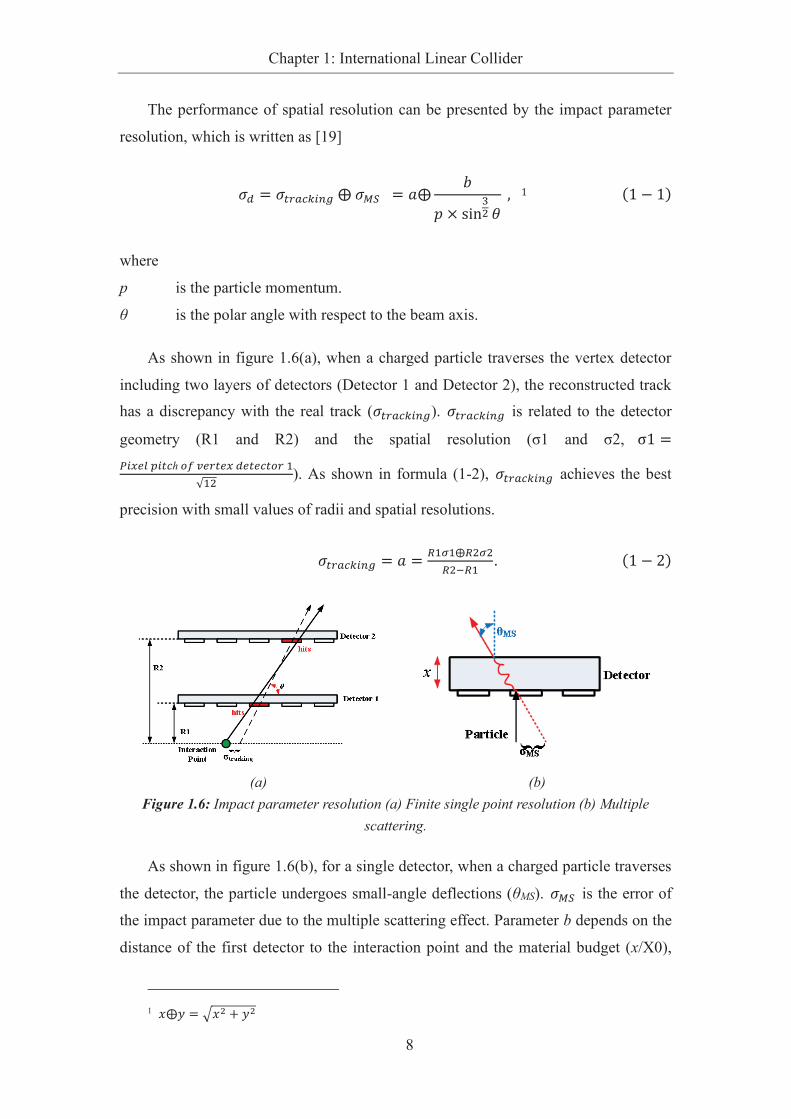
The performance of spatial resolution can be presented by the impact parameter
resolution, which is written as [19]
!" = !#$%&'()*+,+!-. ++= /, 01 × sin23 4 +5+++1+++++++++++++++++++++++++++67 8 79 where
p is the particle momentum.
θ is the polar angle with respect to the beam axis.
As shown in figure 1.6(a), when a charged particle traverses the vertex detector
including two layers of detectors (Detector 1 and Detector 2), the reconstructed track
has a discrepancy with the real track (!#$%&'()*). !#$%&'()* is related to the detector
geometry (R1 and R2) and the spatial resolution (σ1 and σ2, +:7 =;(<>?+@(#&ℎ+AB+C>$#><+">#>&#A$+DED3 ). As shown in formula (1-2), !#$%&'()* achieves the best
precision with small values of radii and spatial resolutions.
!#$%&'()* = / = FDGD,F3G3F3HFD I+++++++++++++++++++++++++++++++++++ 67 8 J9
(a) (b)
Figure 1.6: Impact parameter resolution (a) Finite single point resolution (b) Multiple
scattering.
As shown in figure 1.6(b), for a single detector, when a charged particle traverses
the detector, the particle undergoes small-angle deflections (θMS). !-. is the error of
the impact parameter due to the multiple scattering effect. Parameter b depends on the
distance of the first detector to the interaction point and the material budget (x/X0),
1 K,L = MK3 N L3

Chapter 1: International Linear Collider
9
where X0 is the radiation length of the scattering medium.
0 = O7 × 7PIQ+6RST9 × U KVW × X7 N WIWPY ln Z KVW[\++++++++++++67 8 P9 Some examples of parameter a and b in formula (1-1) for other experiments are
shown in table 1-2. Parameter a and b are set as ≤ 5 (µm) and ≤ 10 (µm‧GeV) for the
ILD.
Table 1-2: Parameter a and b for detectors.
a (µm) b (µm‧GeV)
LEP 25 70
SLD 8 33
LHC 12 70
RHIC-II 13 19
ILD ≤5 ≤10
The impact parameter resolution of ILD (a=5 µm and b=10 µm‧GeV) is simulated
according to the formula (1-1). As shown in figure 1.7, the polar angle (θ) is fixed (30,
60, 90 degrees), the impact parameter resolution increases as the momentum of the
charged particle decreases. The track generated by a low momentum charged particle
will make larger deflection than that by a high momentum charged particle.
Figure 1.7: Impact parameter resolution as a function of the particle momentum.
Requirements
In order to meet experimental conditions and the impact parameter resolution of
the ILC, requirements for the ILD are as follows:
Chapter 1: International Linear Collider
10
Ø Read-out time ~2-9 µs
Ø Spatial resolution: <= 3 μm (corresponding to a pitch of ~17 µm);
Ø Material budget: O(0.15% X0/layer);
Ø A first layer located at a radius of ~1.6 cm;
Ø Occupancy: ~ 5 part/cm2/BX.
Ø Radiation hardness: O(100kRad) and O(1×10¹¹neq(1Mev)) /year (layer 1).
Ø Power dispation: ~50 mW / cm2.
Geometries
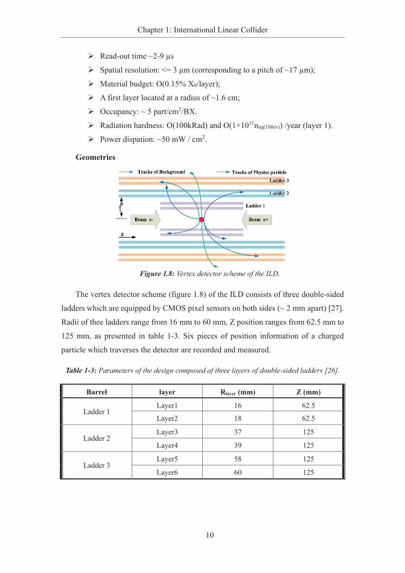
Figure 1.8: Vertex detector scheme of the ILD.
The vertex detector scheme (figure 1.8) of the ILD consists of three double-sided
ladders which are equipped by CMOS pixel sensors on both sides (~ 2 mm apart) [27].
Radii of thee ladders range from 16 mm to 60 mm, Z position ranges from 62.5 mm to
125 mm, as presented in table 1-3. Six pieces of position information of a charged
particle which traverses the detector are recorded and measured.
Table 1-3: Parameters of the design composed of three layers of double-sided ladders [26].
Barrel layer Rlayer (mm) Z (mm)
Ladder 1 Layer1 16 62.5
Layer2 18 62.5
Ladder 2 Layer3 37 125
Layer4 39 125
Ladder 3 Layer5 58 125
Layer6 60 125

Chapter 1: International Linear Collider
11
1.3.2 Silicon Tracking Part
The silicon tracking part is a complement component of the main tracking system
for the track reconstruction capability. It is made up of four components to measure
particles’ momenta, including the Silicon Inner Tracker (SIT), the Silicon External
Tracker (SET), the Forward Tracking Detector (FTD) and the Endcap Tracking
Detector (ETD).
Figure 1.9: ILD schemes of the silicon tracking system.
As shown in figure 1.9, the SIT and the SET are barrel components. The SIT is
positioned between the vertex detector and the TPC, and constituted by 2 double layers
of CMOS pixels sensors. The SET is located between the TPC and the Electromagnetic
CALorimeter (ECAL, see figure 1.5), it is composed of 2 layers of silicon strip
detectors. The FTD consists of 7 tracking disks that are positioned between the beam
pipe and the TPC, the first two disks which are closed to the vertex detector are pixel
detectors and the other five disks are silicon strip detectors. The ETD is located
between the TPC end plate and the ECAL, providing a precise point for tracks that go
into the endcap [26][28].
1.3.3 Time Projection Chamber
The Time Projection Chamber (TPC) is a central component of the main tracking
system. It is about 4.6 m in length, from 33 cm to 180 cm in radii. The TPC is optimised
for 3-dimensional point resolution (better than 100 µm in rφ, and about 1 mm in Z)
which provides large accuracy for the reconstruction. For charged particles with
momenta above 100 MeV, the tracking efficiency up to nearly 100% simulated
realistically with full backgrounds. The TPC providing particle identification

Chapter 1: International Linear Collider
12
capabilities by the specific energy loss (dE/dx).
1.3.4 Calorimeter System
Calorimeters are used to measure the energy of a particle. In the particle flow
approach, all particles in an event are reconstructed individually. The calorimeter
system for ILD consists of a nearly cylindrical barrel calorimeter and two large end cap
calorimeters. Each calorimeter is composed of the ECAL and the Hadronic
CALorimeter (HCAL), which is designed to identify photons and neutral hadrons
respectively and measure their energy.
1.3.5 Muon System
The muon system is used to identify muons in the ILD by some measurement
stations outside the solenoid coil. It is implemented by square tiles of 30×30 mm2 and a
thickness of 10 mm, with the Silicon PhotoMultiplier (SiPM) readout.
1.3.6 Coil and Yoke System
A large volume superconduction coil surrounding calorimeters is used to supply
the magnetic field for a nominal 3.5 T and maximum 4 T solenoidal central field. The
iron yoke surrounding the coil is used to identify muons and catch tails of hadronic
showers. It returns the flux of the magnetic and reduces the outside stray fields.
1.4 Motivation
There are a large amount of hits generated by charged particles coming from the
beam background (low momentum). Our group in the IPHC proposed to integrate the
Artificial Neural Network into CMOS pixel sensor to tag and remove hits generated by
these particles. The motivation of the concept is described in the section.
1.4.1 Challenges for Track Reconstruction
For the ILC program at the centre-of-mass energy of 250 GeV, data rate

Chapter 1: International Linear Collider
13
requirement for the vertex detector is ~3 Gbits/s with the safety factor of 3, which is
~30%-50% data flow of the total system. A large fraction of the data flow is related to
hits generated by particles coming from the beam background. As simulation result
shown in figure 1.10, 104 hits are generated on the layer 1 of the vertex detector by
particles with momenta of 10 MeV/c. Particles from the beam background have typical
lower momenta (~10-100 MeV/c) [19] than particles coming from the physics process.
Figure 1.10: Beam background features simulation [29].
Track reconstruction for low-momentum particles is challenging. Due to the
multiple scattering effect, particles with low momenta make obvious deflections when
they are traversing a layer of the detector leading to the failure of reconstruction. In
figure 1.11, hits and tracks of different momentum particles in a 6-layer detector are
presented and compared. Firstly, these deflections formed by low momentum particles
produce many segments of different layers, which cannot be merged. Secondly, low
momentum particles creating large deflections on the track may hit only one layer of
the detector (just a single hit), resulting in the lack of information for reconstruction.
Figure 1.11: Schematic diagram of tracks generated by particles, one is created by a particle
with high momentum (blue) and others are created by particles with low momenta.

Chapter 1: International Linear Collider
14
1.4.2 Trajectory of Charged Particles
In detectors of the ILC, under the effect of the magnetic field, charged particles
move along the helix trajectory. The helix trajectory is shown in figure 1.12. Vertex
represents the vertex detector of the ILD, z presents the beam direction, the momentum
(P) of the particle is decomposed into the transverse momentum (PT) and the
momentum along the Z-axis (PZ).
Figure 1.12: Helix trajectory of charged particles under the effect of the magnetic field.
The trajectory is projected on both the transverse and parallel plane respectively to
illustrate and analyse.
Trajectory Projected on Transverse Plane
As indicated in figure 1.13, the trajectory of an electron (e-) is projected on the
transverse plane (plane xy) and presents a circle movement. The electron hits on the
vertex detector and the incident angle projected is named θT.
Figure 1.13: Trajectory projection of a charged particle on the transverse plane.
The centripetal force of the electron is supplied by the Lorentz force:

Chapter 1: International Linear Collider
15
]^_ = `a^3O 5++++++++++++++++++++++++++++++++++++++++++++++++67 8 b9 Where
v is the speed of the electron.
B is the magnetic field perpendicular to the direction of the electron, measured in
Tesla.
q is the electron charge.
m is the rest mass of the electron.
γ is a constant value.
R is the radius of the trajectory measured in meter.
According to formula (1-4), the momentum of the electron in the magnetic field is
expressed as
c = `a^ = ]_O+5 Zdefghj+km‧ah [I++++++++++++++++++++++++++67 8 o9
Applying unit conversion to the formula (1-5), the transverse momentum is
cp q WIP × _rtu × Orau5+++vdefgh w xSTy z++5+++++++++++++++++++++++67 8 Q9 According to formula (1-6), the minimum transverse momentum required for an
electron to arrive at different layers is as follows (without the influence of energy loss
and scattering in the trajectory and B = 3.5 T):
Table 1-4: Minimum transverse momentum of a particle to arrive different layers (Rlayer is the
radius of the vertex detector and R is the radius of the particle trajectory).
Layer Rlayer(mm) R(mm) PT(MeV/c)
1 16 8 8.4
2 18 9 9.5
3 37 19.5 19.5
4 39 19.5 20.5
5 58 29 30.5
6 60 30 31.5
In figure 1.13, incident angle 4p . is the angle between the tangent line at the hit
point and the normal line of the vertex detector, calculated as

Chapter 1: International Linear Collider
16
4p = {J 8 /|y}h vO?%~>$DJ × O z = {J 8 /|y}h vWIP × _ × O?%~>$DJ × cp z5+++++++67 8 �9 where
Rlayer1 is the radius of the first layer vertex detector, which is 16mm [26].
According to formula (1-7), θT as a function of the transverse momentum is plotted
in figure 1.14. θT decreases as the transverse momentum of the particle increases.
Particles from the beam background (typical 10-100 MeV/c) [19] possess larger
incident angles than particles from the physics event due to low momenta.
Figure 1.14: Incident angle θT as a function of the particle transverse momentum (PT).
Trajectory Projected on Parallel Plane
In figure 1.15, the trajectory of the electron projected on a parallel plane, where
Z-axis represents the beam line, Vertex layer 1 presents the location of the ladder 1
whose |Z| is 62.5 mm [26], be is the angle between the trajectory and Z-axis,
4� = �����n vO?%~>$DK z5++++++++++++++++++++++++++++++++67 8 Y9 where
x is the distance along the Z-axis from the interaction point to the hit location.

Chapter 1: International Linear Collider
17
Figure 1.15: Trajectory projection of a charged particle on the parallel plane.
Minimum angle be that can generate a hit on the vertex detector is 14.36 degrees,
calculated as
4��() = �����n vO?%~>$D��� z = �����n v 7QQJIoz = 7bIPQ+6�Sm9I++++++++67 8 �9 1.4.3 Principle for Particle Recognition
Considering the artificial neural network successfully applied in many fields of
pattern recognition, our group in the IPHC proposed a CMOS pixel sensor with
artificial neural networks to identify and remove hits generated by particles from the
beam background for reducing the bandwidth (maximum rate of data transfer) of the
data stream and improving tracking capability.
Figure 1.16: Schematic diagram of an incident angle on the vertex detector.
As shown in figure 1.16, angle θb and θT is the projection of the incident angle (θ)
on two planes respectively. Under the situation that θb has a fixed value, the incident
angle (θ) increases as the particle transverse momentum decreases (PT). Particles from
the beam background (typical lower momenta) possess larger incident angles into the
vertex detector than those of particles from physics events.

Chapter 1: International Linear Collider
18
Figure 1.17: Cluster shapes generated by particles from the physics process and particles from
the beam background.
When a charged particle passing through the epitaxial layer of the CPS vertex
detector, electron-hole pairs are created by the ionization process about typical ~80
e-h/µm. Electrons are collected by the diode in each pixel. If the hit is at nearby the
border of pixels, electrons would be collected by two or more independent pixels.
These independent pixels constitute a charge cluster which expresses hit information.
Especially with the decrease in the size of the pixel geometry, the charge-sharing effect
becomes more obvious and important [30][31][32]. In figure 1.17, the larger incident
angle of a background particle leads to producing an elongated cluster shape. The
difference in clusters generated by the two particles makes it possible to tag and remove
hits generated by background particles using artificial neural networks.
1.5 Summary
The ILC project and the motivation of a CMOS pixel sensor with on-chip artificial
neural networks are introduced in the chapter. In the ILC, a large amount of hits are
generated by particles coming from the beam background which have low momenta.
Due to the multiple scattering, tracks make large deflections for these particles, leading
to the failure on the track reconstruction. Our group propose a CPS with on-chip ANNs
to tag and remove hits generated by these particles. Under the effect of the magnetic
field, particles with low momenta produce large incident angles on the vertex detector
and create elongated cluster shapes. An ANN is implemented to reconstruct the
incident angle and tag the hit.
The principle and technology of semiconductor detector will be introduced in the
next chapter.

Chapter 1: International Linear Collider
19
1.6 Bibliography
[1]. https://home.cern/science/physics/standard-model
[2]. Brau, James, Yasuhiro Okada, and Nicholas Walker. "Ilc reference design report volume
1-executive summary." arXiv preprint arXiv:0712.1950 (2007).
[3]. Edwards, Donald A., and Michael J. Syphers. An introduction to the physics of high energy
accelerators. John Wiley & Sons, 2008.
[4]. Wille, Klaus. The physics of particle accelerators: an introduction. Clarendon Press,
2000.
[5]. https://ilchome.web.cern.ch/ilc/project
[6]. https://home.cern/science/accelerators/large-hadron-collider
[7]. Bambade, Philip, et al. "The International Linear Collider: A Global Project." arXiv
preprint arXiv:1903.01629 (2019).
[8]. Barish, Barry, and James E. Brau. "The International Linear Collider." International
Journal of Modern Physics A 28.27 (2013): 1330039.
[9]. Behnke, Ties. "The international linear collider." Fortschritte der Physik 58.7‐9 (2010):
622-627.
[10]. Adams, T., et al. "Terascale physics opportunities at a high statistics, high energy neutrino
scattering experiment: nuSOnG." International Journal of Modern Physics A 24.04
(2009): 671-717.
[11]. Loew, Gregory A. "Report from the international linear collider technical review
committee." Proceedings of the 2003 Particle Accelerator Conference. Vol. 1. IEEE,
2003.
[12]. Loew, Gregory. International Linear Collider Technical Review Committee: Second
Report, 2003. No. SLAC-R-606. Stanford Linear Accelerator Center, Menlo Park, CA
(US), 2003.
[13]. Adolphsen, Chris. The International Linear Collider Technical Design Report-Volume 3.
II: Accelerator Baseline Design. No. arXiv: 1306.6328; ILC-REPORT-2013-040;
ANL-HEP-TR-13-20; BNL-100603-2013-IR; IRFU-13-59; CERN-ATS-2013-037;
COCKCROFT-13-10; CLNS-13-2085; DESY-13-062; FERMILAB-TM-2554;
IHEP-AC-ILC-2013-001; INFN-13-04-LNF; JAI-2013-001; JINR-E9-2013-35;
JLAB-R-2013-01; KEK-REPORT-2013-1; KNU-CHEP-ILC-2013-1; LLNL-TR-635539;
SLAC-R-1004; ILC-HIGRADE-REPORT-2013-003. Argonne National Lab.(ANL),

Chapter 1: International Linear Collider
20
Argonne, IL (United States); Thomas Jefferson National Accelerator Facility (TJNAF),
Newport News, VA (United States); Brookhaven National Laboratory (BNL), Upton, NY
(United States); SLAC National Accelerator Lab., Menlo Park, CA (United States); Fermi
National Accelerator Lab.(FNAL), Batavia, IL (United States), 2013.
[14]. Adolphsen, Chris. The International Linear Collider Technical Design Report-Volume 3.
I: Accelerator\& in the Technical Design Phase. No. arXiv: 1306.6353;
ILC-REPORT-2013-040; ANL-HEP-TR-13-20; BNL-100603-2013-IR; IRFU-13-59;
CERN-ATS-2013-037; COCKCROFT-13-10; CLNS-13-2085; DESY-13-062;
FERMILAB-TM-2554; IHEP-AC-ILC-2013-001; INFN-13-04-LNF; JAI-2013-001;
JINR-E9-2013-35; JLAB-R-2013-01; KEK-REPORT-2013-1; KNU-CHEP-ILC-2013-1;
LLNL-TR-635539; SLAC-R-1004; ILC-HIGRADE-REPORT-2013-003. Argonne
National Lab.(ANL), Argonne, IL (United States); Thomas Jefferson National Accelerator
Facility (TJNAF), Newport News, VA (United States); Brookhaven National Laboratory
(BNL), Upton, NY (United States); SLAC National Accelerator Lab., Menlo Park, CA
(United States); Fermi National Accelerator Lab.(FNAL), Batavia, IL (United States),
2013.
[15]. Japan Association of High Energy Physicists (JAHEP), “A proposal for a phased
execution of the international linear collider project,” http://www.jahep.org/
office/doc/201210_ILC_staging_e.pdf (2012).
[16]. Bambade, Philip, et al. "The International Linear Collider. A European
Perspective." arXiv preprint arXiv:1901.09825(2019).
[17]. Baer, Howard, et al. "The International linear collider technical design report-volume 2:
physics." arXiv preprint arXiv:1306.6352 (2013).
[18]. https://cds.cern.ch/record/2655225/files/TDR-machine-layout-cartoon-staged-mirror.pn
g
[19]. Besson, Auguste Guillaume. "The ILC Vertex Detector requirements." PoS (2017): 047.
[20]. Vogel, Adrian. "Beam-induced backgrounds in detectors at the ILC." (2008).
[21]. Yokoya, Kaoru, and Pisin Chen. "Beam-beam phenomena in linear colliders." Frontiers
of Particle Beams: Intensity Limitations. Springer, Berlin, Heidelberg, 1992. 415-445.
[22]. Chen, Pisin. Disruption, beamstrahlung, and beamstrahlung pair creation. No.
SLAC-PUB-4822; CONF-8806243-31. Stanford Linear Accelerator Center, Menlo Park,
CA (USA), 1988.
[23]. Zolotorev, M. S., E. A. Kuraev, and V. G. Serbo. Estimates of electromagnetic
background processes for the VLEPP project. No. SLAC-TRANS-0227. 1987.

Chapter 1: International Linear Collider
21
[24]. Parker, Brett, et al. Functional Requirements on the Design of the Detectors and the
Interaction Region of an e+e- Linear Collider with a Push-Pull Arrangement of Detectors.
No. SLAC-PUB-13657. 2009.
[25]. Tim Barklow. The SiD Detector at ILC, The European Physical Society Conference on
High Energy Physics (EPS-HEP) 2017, Venice, Italy, July 08, 2017.
[26]. Behnke, Ties. The international linear collider technical design report-volume 4:
detectors. No. arXiv: 1306.6329; ILC-REPORT-2013-040; ANL-HEP-TR-13-20;
BNL-100603-2013-IR; IRFU-13-59; CERN-ATS-2013-037; COCKCROFT-13-10;
CLNS-13-2085; DESY-13-062; FERMILAB-TM-2554; IHEP-AC-ILC-2013-001;
INFN-13-04-LNF; JAI-2013-001; JINR-E9-2013-35; JLAB-R-2013-01;
KEK-REPORT-2013-1; KNU-CHEP-ILC-2013-1; LLNL-TR-635539; SLAC-R-1004;
ILC-HIGRADE-REPORT-2013-003. Argonne National Lab.(ANL), Argonne, IL (United
States); Pacific Northwest National Lab.(PNNL), Richland, WA (United States); SLAC
National Accelerator Lab., Menlo Park, CA (United States); Fermi National Accelerator
Lab.(FNAL), Batavia, IL (United States), 2013.
[27]. Simon, Frank. "Higgs Physics at future Linear Colliders-A Case for precise
Vertexing." arXiv preprint arXiv:1401.6302(2014).
[28]. The ILD Detector at the ILC, “Ties Behnke Deutsches Elektronen Synchroton, DESY,
Germany.https://indico.cern.ch/event/765096/contributions/3295752/attachments/178527
6/2906298/ILD_European_Strategy_Document.pdf
[29]. A. Perez , et al. "Beamstrahlung background simulation status report", AWLC 2017
workshop, June 30, 2017.
[30]. Maj, P., et al. "Comparison of the charge sharing effect in two hybrid pixel detectors of
different thickness." Journal of Instrumentation 10.02 (2015): C02006.
[31]. Maj, P., et al. "Algorithms for minimization of charge sharing effects in a hybrid pixel
detector taking into account hardware limitations in deep submicron technology." Journal
of Instrumentation 7.12 (2012): C12020.
[32]. Mathieson, K., et al. "Charge sharing in silicon pixel detectors." Nuclear Instruments and
Methods in Physics Research Section A: Accelerators, Spectrometers, Detectors and
Associated Equipment 487.1-2 (2002): 113-122.

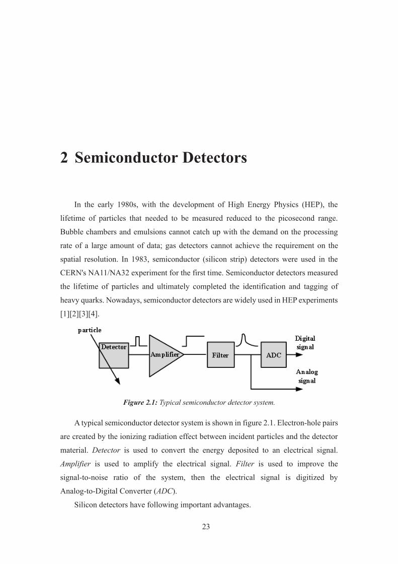
23
2 Semiconductor Detectors
In the early 1980s, with the development of High Energy Physics (HEP), the
lifetime of particles that needed to be measured reduced to the picosecond range.
Bubble chambers and emulsions cannot catch up with the demand on the processing
rate of a large amount of data; gas detectors cannot achieve the requirement on the
spatial resolution. In 1983, semiconductor (silicon strip) detectors were used in the
CERN's NA11/NA32 experiment for the first time. Semiconductor detectors measured
the lifetime of particles and ultimately completed the identification and tagging of
heavy quarks. Nowadays, semiconductor detectors are widely used in HEP experiments
[1][2][3][4].
Figure 2.1: Typical semiconductor detector system.
A typical semiconductor detector system is shown in figure 2.1. Electron-hole pairs
are created by the ionizing radiation effect between incident particles and the detector
material. Detector is used to convert the energy deposited to an electrical signal.
Amplifier is used to amplify the electrical signal. Filter is used to improve the
signal-to-noise ratio of the system, then the electrical signal is digitized by
Analog-to-Digital Converter (ADC).
Silicon detectors have following important advantages.

Chapter 2: Semiconductor Detectors
24
Ø Low ionization energy
Average 3.6 eV energy is needed to generate one electron-hole pair in
silicon detectors. 30 eV energy is needed for gas detectors to generate one
electron-ion pair.
Ø High density
Due to the high density of silicon material, the number of electron-hole
pairs are large. For a Minimum Ionizing Particle (MIP), the number of
ionized electron-hole pairs is about 80 e-/um, the average energy loss is about
300 eV/µm (3.6 eV/e-h).
Ø Fast signal speed
Compared with liquid or gas detectors, silicon detectors process the
electrical signal fast.
Basic properties and types of semiconductor detectors (Si detector) are described in
the chapter. Firstly, generation and transportation of carriers in semiconductor detectors
are described. Then, basic components of semiconductor detectors, the P-N junction
and the MOS structure, are introduced. Finally, various kinds of semiconductor
detectors are given and compared.
2.1 Carriers Generation
In this section, the generation of carriers is described based on two types of
particles: photons and charged particles.
2.1.1 Carriers Generated by Photons
An incident photon is absorbed or scattered when it passes through semiconductor
detectors. The energy loss of the incident photon is produced since the physical process
including the Photoelectric effect, the Compton effect and the Electron-Positron pair
production. Contributions of different physical processes depend on the photon energy
and the material.
As illustrated in figure 2.2, if the energy loss of the photon is greater or equal to the
energy of the band gap (EG), an electron will be lifted to the conduction band and a hole
will be left in the valence band. If the energy loss is less than the energy of the band gap

Chapter 2: Semiconductor Detectors
25
(EG), it is possible that the photon would be absorbed since local states in the band gap
due to lattice imperfections exist [5].
Figure 2.2: Generation of electrons and holes by absorption of photons, the energy loss=
Eg, >Eg, and < Eg [5].
2.1.2 Carriers Generation by Charged Particles
A charged particle passes through semiconductor detectors, due to the ionization
effect, electron-hole pairs will be created around the track. The average energy of the
charged particle used to create an electron-hole pair is 3.6 eV which is about three times
larger than the band gap of 1.1 eV. The average energy loss of the charged particle can
be calculated as the Bethe-Bloch formula (2-1):
8���K = b{��|>3a>y3�3 ���3 �7J �e Ja>y3�3`3t�%<�3 8 �3 8 7J�6`9�I+++++6J 8 79 In formula (2-1), NA is the Avogadro’s number (6.0221415×10²³mol-1), re is the
classical electron radius, me is the electron mass, c is the velocity of light, z is the charge
of the incident particle. Z is the atomic number of the absorber. Tmax is the maximum
kinetic energy that can be imparted to a free electron in a single collision, I is the mean
excitation energy, β is the relativistic boost and the γ is the Lorentz factor. The term δ is
a density correction. The unit of results is MeV g−1cm2 [6][7].

Chapter 2: Semiconductor Detectors
26
2.2 Carriers Transport
In semiconductor detectors, currents are generated by the movement of free
carriers. Two types of currents are introduced to describe the transportation of free
carriers in the semiconductor: The drift current and the diffusion current.
2.2.1 Drift
The drift current is formed due to an external electric field applied to
semiconductor detectors. Free carriers (electrons and holes) are forced by the electric
field in different directions.
�)"$(B# = ]e�)�+I+++++++++++++++++++++++++++++++++++++++++++6J 8 J9 �@"$(B# = ]1�@�+I++++++++++++++++++++++++++++++++++++++++++++6J 8 P9!
The density of the electron and hole drift current (A/cm2) is expressed as formula
(2-2) and (2-3), respectively: p and n are the number of holes and electrons per cubic
centimetre; q is the elementary charge (1.602×10⁻¹⁹ C); µn and µp are the mobility of
electrons and holes, with the unit of cm2/V‧s; E is the electric field with the unit of V/cm.
The total density of the drift current is:
�"$(B# = ]e�)� N ]1�@�+I++++++++++++++++++++++++++++++6J 8 b9 2.2.2 Diffusion
The diffusion current is formed thanks to the variation of the carrier concentration.
Free carriers move from the high concentration region to the low concentration region
when there is a difference between concentration gradients of the two regions. The
density of the diffusion current (A/cm2) is expressed in formula (2-5) and (2-6),
respectively: Dp and Dn are diffusion coefficients for holes and electrons; p and n are
the number of holes and electrons per cubic centimetre; q is the elementary charge.
�)"(BB = +++]�) �e�K I++++++++++++++++++++++++++++++++++++++++++++6J 8 o9

Chapter 2: Semiconductor Detectors
27
�@"(BB = 8]�@ �1�K I+++++++++++++++++++++++++++++++++++++++++++6J 8 Q9 The total density of the diffusion current is:
�"(BB = ]�) �e�K +8 ]�@ �1�K ++++++++++++++++++++++++++++++++++6J 8 �9 2.3 P-N Junction
(a) (b)
Figure 2.3: P-N junction (a) Depletion region (b) Energy band diagram.
P-N junctions are basic structures of semiconductor electronics. A P-N junction
(figure 2.3 (a)) is produced by joining together the N-type and P-type semiconductor.
The principle of the P-N junction is described as follows: Firstly, free electrons in
the N-type side diffuse to the P-type side and overcome the junction. Then, the free
electrons recombine with holes nearby the junction in the P-type side. Donor ions left in
the N-type side are positively charged and acceptor ions left in the P-type side are
negatively charged. As a result, a built-in electric field pointing from N-type to P-type
is created. The built-in electric field rejects the diffusion of carriers and keeps the
dynamic equilibrium of the concentration.
No free charge carriers can rest in the region located around the junction between
two sides, which is named the depletion region. According to the energy band
schematic shown in figure 2.3 (b), it implies that extra energy is needed to transport an
electron to overcome the depletion region.
The state of the P-N junction will be changed if the extra bias is applied. States
under the forward bias and the reverse bias are described. The drift current in the P-N
junction is not changed with the variety of the bias voltage as the number of minority
charge carriers is limited [8][9].

Chapter 2: Semiconductor Detectors
28
2.3.1 Forward Bias
(a) (b)
Figure 2.4: P-N junction under forward bias (a) Depletion region (b) Energy band diagram.
In figure 2.4 (a), a forward bias is applied to the P-N junction, which means that the
P-type side is connected to a positive voltage and the N-type side is connected to a
negative voltage. The negative voltage pushes free electrons in the N-type side move to
the depletion region and recombine with holes, leading to the depletion region thinner
and the built-in electric field weakened. In figure 2.4 (b), the barrier of the depletion
region decreases, and the energy required to transport an electron reduces under the
forward bias.
2.3.2 Reverse Bias
(a) (b)
Figure 2.5: P-N junction under reverse bias (a) Depletion region (b) Energy band diagram.
In figure 2.5 (a), a reverse bias is applied to the P-N junction. Electrons nearby the
junction are attracted by the positive voltage applied to the N-type side, move away
from the depletion region, leading to the depletion region wider and the built-in electric
field strengthened. In figure 2.5 (b), the barrier of the depletion region is increased

Chapter 2: Semiconductor Detectors
29
under reversed bias and the energy used to transport electrons from the N-type side to
the P-type side becomes large.
2.4 Metal-Oxide-Semiconductor
Figure 2.6: N-type Metal-Oxide-Semiconductor structure.
The Metal-Oxide-Semiconductor (MOS) diode is a basic structure used in the
semiconductor device. It is composed of three layers, an oxide layer, a metal layer
called gate (G) and a P-type or N-type semiconductor layer named substrate or body (B).
An N-type channel MOS structure is shown in figure 2.6. Heavily doped polysilicon
layers are often used instead of gate metal. Typically, voltages are applied to the gate
(VG) and body contact (VB).
Figure 2.7: An n-type MOS under accumulation, depletion and inversion conditions [10].
Three bias modes (accumulation, depletion and inversion, see figure 2.7) and
corresponding capacitance of the MOS diode are varied with the bias voltage applied to
the gate and the body (VGB). VFB is the flat band voltage which makes the energy band
of the semiconductor side present horizontally. The flat band indicates that there is no
charge present in the oxide or at the oxide-semiconductor interface. In traditional
MOSFET models, VT is defined as the gate voltage that will drive the channel under the
gate into strong charge inversion cases [11].

Chapter 2: Semiconductor Detectors
30
Accumulation
In the case of accumulation, the voltage applied to the gate and body contact is less
than the flatband voltage (VGB < VFB). Carrier densities change accordingly in its
surface region. Negative and positive charges are induced in the gate and the body,
respectively. Holes are accumulated under the oxide-semiconductor interface.
Depletion
In the case of depletion, the voltage applied to the gate and body contact is larger
than the flat band voltage and less than the threshold voltage (VFB < VGB < VT). Positive
charges are produced at the interface between the metal gate and the oxide. Holes in the
body are repelled and a depletion region is created.
Inversion
In the case of inversion, the voltage applied to the gate and substrate contact is
larger than the threshold voltage (VT < VGB). With the voltage VGB increases, negative
charges created at the interface become more and the depletion region is wider, leading
to the surface of semiconductor inverts to N-type, an inversion layer is formed.
2.5 Silicon Detector Types
With the development of physics and the improvement for various HEP
experiments, several types of silicon detectors have been proposed and established.
Including strip detectors, Charged Coupled Devices (CCDs), hybrid pixel detectors,
DEPleted Field Effect Transistor (DEPFET) detectors and Monolithic Active Pixel
Sensors (MAPS) are introduced.
2.5.1 Strip Detector
With the introduction of the planar process proposed by Krammer in 1980 to
replace the technology of surface barrier, high-quality silicon detectors that have
extremely low reverse currents can be implemented [12]. Thanks to the technology of
photolithography, requirements on resolution and rate can be achieved by dividing the
sensor into segments. Single-sided and double-sided strip detectors are described.
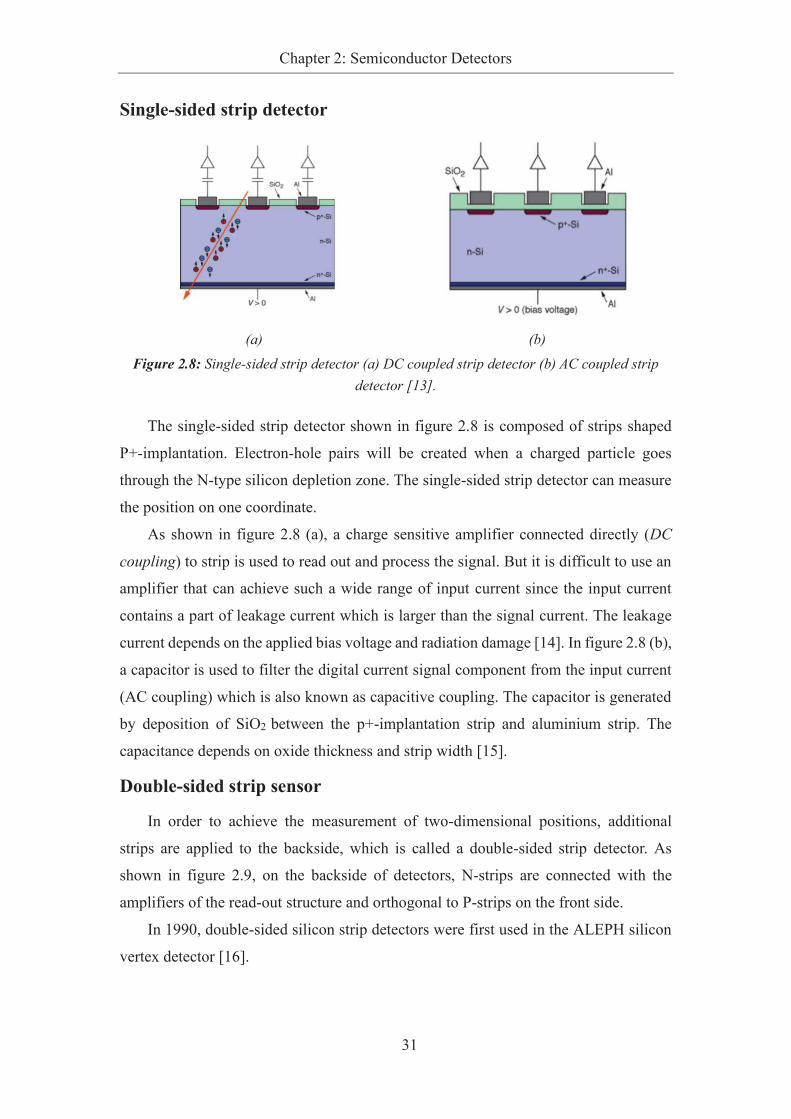
Chapter 2: Semiconductor Detectors
31
Single-sided strip detector
(a) (b)
Figure 2.8: Single-sided strip detector (a) DC coupled strip detector (b) AC coupled strip
detector [13].
The single-sided strip detector shown in figure 2.8 is composed of strips shaped
P+-implantation. Electron-hole pairs will be created when a charged particle goes
through the N-type silicon depletion zone. The single-sided strip detector can measure
the position on one coordinate.
As shown in figure 2.8 (a), a charge sensitive amplifier connected directly (DC
coupling) to strip is used to read out and process the signal. But it is difficult to use an
amplifier that can achieve such a wide range of input current since the input current
contains a part of leakage current which is larger than the signal current. The leakage
current depends on the applied bias voltage and radiation damage [14]. In figure 2.8 (b),
a capacitor is used to filter the digital current signal component from the input current
(AC coupling) which is also known as capacitive coupling. The capacitor is generated
by deposition of SiO2 between the p+-implantation strip and aluminium strip. The
capacitance depends on oxide thickness and strip width [15].
Double-sided strip sensor
In order to achieve the measurement of two-dimensional positions, additional
strips are applied to the backside, which is called a double-sided strip detector. As
shown in figure 2.9, on the backside of detectors, N-strips are connected with the
amplifiers of the read-out structure and orthogonal to P-strips on the front side.
In 1990, double-sided silicon strip detectors were first used in the ALEPH silicon
vertex detector [16].

Chapter 2: Semiconductor Detectors
32
Figure 2.9: Operation principle of a double-sided strip detector [17].
2.5.2 CCD
CCDs are built in a pixel array structure based on blocks of MOS capacitors. As
shown in figure 2.10, each pixel is subdivided into three parts by gate elements.
Positive voltages are applied to gates to generate potential wells in the substrate.
Electrons created by incident particles are stored in potential wells, which is illustrated
as a collection of grey. The charge is transferred along each column from pixel to pixel
to the read-out node via controlling voltages of gates.
Figure 2.10: Timing diagram of voltage schemes to transport charge through a three-phase
CCD.
The timing diagram to transport charges through a three-phase CCD system is
shown in figure 2.10. Three gates in each pixel are controlled by the clock signal P1, P2

Chapter 2: Semiconductor Detectors
33
and P3, respectively. All pulsed of three clock signals have a duty cycle of 50% and
their mutual phase shift is 120 degree. At t(0), signal P1 and P3 are held low while
signal P2 is held high. A potential well is created under the gate controlled by P2 of
pixel 1. At t(1), signal P3 is lifted to the high level to make the charge transport from the
gate to the next one [18][19].
CCD structures were first used in the vertex detector of the NA32 experiment in
1983, and then 96 two-dimensional CCDs with a total of 307 Mpixel were used in the
SLD’s upgraded vertex detector [20].
2.5.3 Hybrid Pixel Sensor
Gaalema proposed a readout chip that can be used with the Ge PIN array to
perform X-ray inspection, which is the first demonstration of the concept of a hybrid
detector [21][22]. A schematic diagram of a single pixel of a hybrid detector is shown in
figure 2.11, where a sensor part is connected to a readout electronics part by using the
bump-bonding process. In the sensor part, electrons and holes are separated by a bias
voltage applied to electrodes. Charge signals are converted and processed in the
read-out electronic part. The material and manufacturing processes of the two parts can
be optimized separately targeting at different applications [23].
Figure 2.11: A simplified schematic diagram of a single pixel in a hybrid silicon detector, it is
composed of a sensor part and a readout electronics part [24].
In 1992, hybrid detectors were first successfully tested in the heavy-ion experiment
WA94 [25]. Four experiments installed on the Large Hadron Collider (LHC) collider
from 1998 to 2006 were equipped with hybrid pixel detectors [26].

Chapter 2: Semiconductor Detectors
34
2.5.4 DEPFET Sensor
Figure 2.12: Schematic layout of the DEPFET [27].
DEPFET structures were proposed in 1980 by J.Kemmer and G.Lutz [28]. The
schematic layout of a DEPFET is shown in figure 2.12. A Field Effect Transistor (FET)
is integrated on the N-type depleted silicon bulk. There is a deep N-doping region under
the FET gate named the internal or the second gate. Electrons generated by incident
particles are collected by the internal gate. Modulation of the transistor channel current
is generated as the potential of the internal gate varies. A positive voltage pulse is
applied to the clear gate to reset electrons [3][27][29].
Vertex detectors in the BELLE II being installed will contain two layers of highly
granular DEPFET Pixel Detector (PXD) [2]. The requirement of spatial resolution is 15
μm, the PXD will have pixel sizes of 50×50 μm2 (Layer 1) and 50×75 μm2 (Layer 2) in
order to achieve the resolution.
2.5.5 Monolithic Active Pixel Sensor
In 2000, researchers of the LEPSI and IReS proposed a Monolithic Active Pixel
Sensor (MPAS) for charged particle tracking and imaging [30]. The MAPS structure
integrates signal sensing and readout electronics on the same substrate. They offer an
attractive balance among granularity, material budget, radiation tolerance and readout
speed [31].
Sensor diode
A schematic of the first-generation of MAPS structure is shown in figure 2.13. A
photodiode is formed by the P-N junction generated between the N-well and the
epitaxial layer (P-type). Doping levels of P-well (P+ type) and P-substrate (P++ type)

Chapter 2: Semiconductor Detectors
35
are higher than the epitaxial layer (P- type), leading to the generation of two potential
barriers. A potential barrier is located at the boundary region between the epitaxial layer
and the P-well. The other potential barrier is located at the boundary region between the
epitaxial layer and the P-substrate.
Figure 2.13: Schematic of the first-generation MAPS structure.
A charged particle traverses the MAPS detector, the energy released by the particle
are converted and typically ~80 electron-hole pairs are generated per micron. Electrons
created in the epitaxial layer diffuse thermally and gather at the N-well collection
electrode. Due to the high level of the P-type doping, more of electrons generated in the
substrate are recombined, just few electrons can drift to the epitaxial layer and be
collected by the collection electrode.
Figure 2.14: Schematic of the second-generation MAPS structure.
In the first-generation MAPS structure, only NMOS transistor can be used in a
pixel. An N-well which is used to host PMOS transistor would compete for charge
collection with N-well/P-epi diodes. In order to avoid this situation, a deep P-well in the
P-substrate is proposed to shield the N-well from the epitaxial layer or substrate in the
second-generation structure, as shown in figure 2.14. The deep P-well prevents the
N-well from collecting electrons, therefore allowing the use of full complementary
CMOS in the pixel [30][32][33].
In pixelated detectors, the electrons diffusion leads to the charge can be shared by
two or more pixels. Especially for smaller pixel size detectors, the effect of charge

Chapter 2: Semiconductor Detectors
36
sharing will be more prominent.
Read-out circuit
A typical in-pixel readout circuit for MAPS structures is shown in figure 2.15,
which is composed of three transistors. M1 is controlled by the signal RESET to reset
the sensing diode. M2 connected to the sensing diode is an input transistor of a source
follower. M3 is controlled by the signal ROW_SEL to select the row of pixel to output.
Figure 2.15: Typical in-pixel readout circuit [30].
The MAPS structure was first used in the vertex detector upgrade of the STAR
(Solenoidal Tracker at RHIC) experiment at RHIC (Relativistic Heavy Ion Collider).
The ALPIDE used in the ALICE experiment is a monolithic pixel sensor will be
fabricated in the 180 nm CMOS imaging sensor process of TowerJazz. It achieves
detection efficiency above 99%, the power consumption less than 40 mW/cm2, a spatial
resolution of around 5 µm. These features all have met even exceeded requirements of
the ALICE experiment, even after neutron irradiation to 1.7×10¹³ 1 MeV neq/cm2 [34].
2.5.6 Conclusions
Single-sided strip detector measures 1 coordinate, while Double-sided strip
detector could give a 2-dimensional position of a particle track. However, the
measurement will be ambiguous, Ghost hits, if more than one particle hits the strip.
Due to the complicated manufacturing procedures, the expensive cost is needed for the
Double-sided strip detector [35]. A limitation for CCD is low readout speed which
depends on the size of the pixel matrix. The charge has to be transferred for long
distances in columns of pixels before reaching the readout line. The Charge Transfer
Efficiency (CTE) is used to measure the quality of the charge transported from one

Chapter 2: Semiconductor Detectors
37
pixel to another, which should be close to 1. CCD is sensitivity to radiation damage,
which makes the charge transfer efficiency degradation. The hybrid pixel sensor
provides low detector capacitance, low leakage current and large signal-to-noise ratio.
Due to a large number of readout channels, large power consumption and expensive
cost are needed [36]. The DEPFET provides an excellent low noise performance which
can achieve a good spatial resolution and a fast readout speed [37]. The DEPFET
detector is not used in a hadron collider since its performance can be destroyed by
additional charges from the radiation damage [6]. Functions of the sensor and amplifier
are combined in the detector. The MAPS structure is manufactured using standard
CMOS technology, leading to some attractive features including low cost, low material
budget, simple readout architecture, high spatial resolution, etc. And the technology
makes it possible to integrate more processing module into circuit. Our concept is to
integrate the ANN into a CMOS pixel sensor to reconstruct the incident angle and tag
the hits generated by particles from the beam background.
Table 2-1: Advantages and disadvantages of these detector technologies [6].
Technology Advantages Disadvantages
Strip detector Large area possible
Fast speed Expensive cost
CCD
Industry standard
High spatial resolution
Integrated amplification
Slow speed
Not radiation hard
Large power consumption
Need different voltages
Hybrid pixel
low detector capacitance
low leakage current
large signal-to-noise ratio
Large channel number
large power consumption
Expensive cost
DEPFET
Integrated amplification
Low power consumption
Low noise
Fast readout speed
Only small devices
Not radiation hard
High power at CLEAR
No industry standard
MAPS
Standard IC process
Integrated amplification
Low noise
Low power
High spatial resolution
Only small devices

Chapter 2: Semiconductor Detectors
38
2.6 Summary
Basic properties and types of semiconductor detectors (Si detector) are described
in the chapter. Generation and transportation of carriers are described. Basic
components, the P-N junction and the MOS structure, also introduced. Typical silicon
detectors used for HEP experiments are introduced and compared. Artificial neural
networks will be introduced briefly in the next chapter.

Chapter 2: Semiconductor Detectors
39
2.7 Bibliography
[1]. Knoll, Glenn F. Radiation detection and measurement. John Wiley & Sons, 2010.
[2]. Hartmann, Frank. "Silicon tracking detectors in high-energy physics." Nuclear Instruments
and Methods in Physics Research Section A: Accelerators, Spectrometers, Detectors and
Associated Equipment 666 (2012): 25-46.
[3]. Moser, Hans-Günther. "Silicon detector systems in high energy physics." Progress in
Particle and Nuclear Physics63.1 (2009): 186-237.
[4]. Michael Moll, "An introduction to Silicon Detectors with focus on High Energy Physics
applications, " SIMDET 2016, 05-07 September 2016, LPNHE Paris.
[5]. Lütz, G. "Semiconductor radiation detectors: Device physics." (2007).
[6]. Hartmann, Frank. Evolution of silicon sensor technology in particle physics. Vol. 231.
Springer, 2008.
[7]. Amsler, C., and Particle Data Group. "1 (2008) and 2009 partial update for the 2010
edition. PL B667." (2009).
[8]. Neamen, Donald A. Semiconductor physics and devices: basic principles. New York, NY:
McGraw-Hill,, 2012.
[9]. Spieler, Helmuth. Semiconductor detector systems. Vol. 12. Oxford university press, 2005.
[10]. Van Zeghbroeck, Bart. "Principles of semiconductor devices." Colarado University 34
(2004).
[11]. Ortiz-Conde, Adelmo, et al. "Revisiting MOSFET threshold voltage extraction
methods." Microelectronics Reliability 53.1 (2013): 90-104.
[12]. Kemmer, Josef. "Fabrication of low noise silicon radiation detectors by the planar
process." Nuclear Instruments and Methods 169.3 (1980): 499-502.
[13]. Silvia Masciocchi, " Semiconductor detectors - 3", SS2017, Heidelberg June 14, 2017.
[14]. http://www.hephy.at/user/friedl/diss/html/node21.html
[15]. Vito Manzari, " Silicon Detectors Lecture 2" , The 5th Egyptian School on High Energy
Physics, 14 – 19, November 2015 Egypt.
[16]. Moser, Hans-Günther. "Experience with the ALEPH silicon vertex detector." Nuclear
Instruments and Methods in Physics Research Section A: Accelerators, Spectrometers,
Detectors and Associated Equipment 310.1-2 (1991): 490-492.
[17]. "5. Silicon Strip Detectors, " MPI HLL

Chapter 2: Semiconductor Detectors
40
[18]. Theuwissen, Albert J. Solid-state imaging with charge-coupled devices. Vol. 1. Springer
Science & Business Media, 2006.
[19]. Janesick, James R. Scientific charge-coupled devices. Vol. 117. Bellingham: SPIE press,
2001.
[20]. Abe, Koya, et al. "Design and performance of the SLD vertex detector: a 307 Mpixel
tracking system." Nuclear Instruments and Methods in Physics Research Section A:
Accelerators, Spectrometers, Detectors and Associated Equipment 400.2-3 (1997):
287-343.
[21]. Gaalema, Steve. "Low noise random-access readout technique for large PIN detector
arrays." IEEE Transactions on Nuclear Science 32.1 (1985): 417-418.
[22]. Heijne, Erik HM. "Semiconductor micropattern pixel detectors: a review of the
beginnings." Nuclear Instruments and Methods in Physics Research Section A:
Accelerators, Spectrometers, Detectors and Associated Equipment 465.1 (2001): 1-26.
[23]. Awadalla, Salah. Solid-state radiation detectors: technology and applications. CRC
Press, 2015.
[24]. Wermes, Norbert. "Pixel detectors for charged particles." Nuclear Instruments and
Methods in Physics Research Section A: Accelerators, Spectrometers, Detectors and
Associated Equipment 604.1-2 (2009): 370-379.
[25]. Beker, H., et al. "A hybrid silicon pixel telescope tested in a heavy-ion
experiment." Nuclear Instruments and Methods in Physics Research Section A:
Accelerators, Spectrometers, Detectors and Associated Equipment 332.1-2 (1993):
188-201.
[26]. Delpierre, P. "A history of hybrid pixel detectors, from high energy physics to medical
imaging." Journal of Instrumentation 9.05 (2014): C05059.
[27]. M. Vos et al., DEPFET active pixel detectors, PoS(VERTEX 2009)015.
[28]. Kemmer, J., and Gerhard Lutz. "New detector concepts." Nuclear Instruments and
Methods in Physics Research Section A: Accelerators, Spectrometers, Detectors and
Associated Equipment 253.3 (1987): 365-377.
[29]. Wermes, Norbert, et al. "New results on DEPFET pixel detectors for radiation imaging
and high energy particle detection." IEEE Transactions on Nuclear Science 51.3 (2004):
1121-1128.
[30]. Turchetta, R., et al. "A monolithic active pixel sensor for charged particle tracking and
imaging using standard VLSI CMOS technology." Nuclear Instruments and Methods in

Chapter 2: Semiconductor Detectors
41
Physics Research Section A: Accelerators, Spectrometers, Detectors and Associated
Equipment 458.3 (2001): 677-689.
[31]. Hu-Guo, Ch, et al. "CMOS pixel sensor development: a fast read-out architecture with
integrated zero suppression." Journal of Instrumentation 4.04 (2009): P04012.
[32]. Snoeys, W. "CMOS monolithic active pixel sensors for high energy physics." Nuclear
Instruments and Methods in Physics Research Section A: Accelerators, Spectrometers,
Detectors and Associated Equipment 765 (2014): 167-171.
[33]. Cavicchioli, C., et al. "Design and characterization of novel monolithic pixel sensors for
the ALICE ITS upgrade." Nuclear Instruments and Methods in Physics Research Section
A: Accelerators, Spectrometers, Detectors and Associated Equipment 765 (2014):
177-182.
[34]. Mager, M., and ALICE Collaboration. "ALPIDE, the Monolithic Active Pixel Sensor for
the ALICE ITS upgrade." Nuclear Instruments and Methods in Physics Research Section
A: Accelerators, Spectrometers, Detectors and Associated Equipment 824 (2016):
434-438.
[35]. Thomas Bergauer. "Silicon Detectors in High Energy Physics", HEPHY Vienna.
http://www.hephy.at/fileadmin/user_upload/Lehre/Unterlagen/Detektoren_Berga
uer/2018/VO-4-2018-SemiconductorDetectors.pdf
[36]. Doris Eckstein. "Solid State Detectors.", DESY.
http://www.desy.de/~garutti/LECTURES/ParticleDetectorSS12/L6_SiliconLectur
e.pdf
[37]. Richter, Rainer Helmut, et al. "Design and technology of DEPFET pixel sensors for linear
collider applications." Nuclear Instruments and Methods in Physics Research Section A:
Accelerators, Spectrometers, Detectors and Associated Equipment 511.1-2 (2003):
250-256.


43
3 Artificial Neural Networks for Pattern
Recognition
Artificial Neural Networks (ANNs) are computational modules that are inspired by
the biological neural network [1]. ANNs, consisting of processing units and
connections (weights) between these units, have been proved to be universal
approximators for a domain of boolean function by the logical calculus [2]. ANNs used
nowadays are evaluated and developed on the basis of the computational model
introduced by Warren McCulloch and Walter Pitts in 1943 [3] and have been used in a
wide variety of field for pattern recognation successfully, including finance, weather,
control, medicine, physics, etc [4][5][6][7].
My thesis propose to integrate ANNs into a CMOS pixel sensor for tagging and
removing hits generated by particles from the beam background. In this chapter, firstly,
the basic principle of artificial neurons are introduced; Next, the Multi-Layer
Perceptron (MLP) which is employed in the thesis, is described; Then, ANN supervised
learning modes and the Back Propagation (BP) algorithm are illustrated. Finally, ANN
applications in the field of high energy physics (HEP) are reviewed briefly.
3.1 Pattern Recognition
Human beings can perform some tasks such as reading hand-written digits,
recognizing traffic signals, etc. Decision processes made by human beings are related to
the identification of patterns in the brain. Pattern recognition is an attempt to grasp the

Chapter 3: Artificial Neural Networks for Pattern Recognition
44
mechanism of decision-making processes and build machines that can perform
decisions like human beings [8][9].
“Pattern recognition is about assigning labels to objects. Objects are
described by a set of measurements called also attributes or features” [10]
When a charged particle passes a CMOS pixel sensor, electrons generated are
collected by several pixels. These pixel values constitute a cluster which presents hit
information of the charged particle. As shown in the figure 3.1, each cluster shape is
represented in a 5×5 pixels matrix. Due to the charged particle from the beam
background have lower momentum than the particle from the physics event, resulting
to generating an elongated cluster shape. We proposed to regress the incident angle of
each cluster by the artificial neural network and then tag and remove hits generated by
charged particles from the beam background.
(a) (b)
Figure 3.1: Examples of cluster shapes (a) Cluster shape generated by charged particles from
the physics event (b) Cluster shape generated by charged a charged particle from the beam
background.
Procedures of pattern recognition are divided into two phases: training and test. As
for the example shown in figure 3.1, in the training phase, training datasets consisting
of lots of cluster shapes and their corresponding incident angles are used to train
parameters (weights) of the machine. Inputted cluster shapes are classed in advance and
their incident angles are known. In the test phase, incident angles are recognized based
on inputted cluster shapes and the weights of the artificial neural network.
In general, pattern recognition is separated into two categories (classification and
regression) according to tasks: In classification tasks, inputs of the machine are
assigned to discrete classes and outputs represent labels of discrete classes. In

Chapter 3: Artificial Neural Networks for Pattern Recognition
45
regression tasks, outputs are values of continuous variables [11].
3.2 Biological and Artificial Neuron
In human brains, biological neural networks which perform decision-making
processes consist of basic components of the biological neuron. Inspired by the
biological neuron, artificial neuron models are proposed and developed as the basic unit
of the ANN. Principles of biological neurons and artificial neurons are introduced in the
section.
3.2.1 Biological Neurons
A human brain has an average of ~100 billion biological neurons that emerge a
wide variety of shapes and sizes in different parts. Biological neurons are
interconnected by synapses. For instance, the pyramidal cell is one of the most common
types of cortical neurons, which can receive 10000 or more synapses [12].
Figure 3.2: Connections between two biological neurons.
Two biological neurons are shown in figure 3.2. Every biological neuron is a single
processing unit. A biological neuron consists of a cell body (soma), an axon and
dendrites. The cell body contains a nucleus which is used to control the cell activity.
Dendrites are used to carry impulse signals generated by other neurons into the cell
body and the axon is used to take impulse signals out from the cell body [12]. The
synapse between the dendrite and an axon terminal of another neuron is used to
converts the electrical signal into a chemical signal, release a neurotransmitter.
The process of the signal generated and transported in a biological neuron as

Chapter 3: Artificial Neural Networks for Pattern Recognition
46
follows: Firstly, neurotransmitters released by previous neurons diffuse across the
synapse. Then, in the receiver neuron, according to the neurotransmitters, input impulse
signals are generated and transmitted to the cell body. The receiver neuron will be
activated if the sum of impulse signals exceeds a threshold. Finally, an output impulse
signal is generated in the cell body and transmitted to the axon. The input impulse
signals can be inhibitory or exciting by neurotransmitters depending on the type of a
synapse. Synapses have the function to learn from activities that they have participated
since their effectiveness is adjusted by impulse signals transported in cell bodies
[13][14].
3.2.2 Artificial Neuron
Artificial neurons, basic components of ANNs, are designed and developed
inspired by the biological neuron. According to the constitution and function, three
elements of an artificial neuron model are identified as follows:
1. Weights. For a biological neural network, two neurons are connected by a
synapse which can be trained by activities. For an artificial neuron, the effect of
a synapse is embodied by the weight between two neurons.
2. A summing junction. For a biological neuron, input impulse signals are
summed up and compared with the threshold. For an artificial neuron, inputs
are weighted and then added together in a summing junction.
3. An activation function. For a biological neuron, a threshold function is used to
determine the neuron is activated or not. For an artificial neuron, including
threshold or other nonlinear functions can be used as activation functions.
Figure 3.3: Computational model of artificial neurons.

Chapter 3: Artificial Neural Networks for Pattern Recognition
47
A computational model of artificial neurons is shown in figure 3.3, where x1, x2….
xn are inputs, x0 is a fixed bias input. w0, w1……wn are corresponding weights. The
value of the summing junction (v) is calculated as
^ =�K( × �( N K� ×��)(�D +I+++++++++++++++++++++++++++++6P 8 79
Then, the value of the summing junction (v) is fed into the activation function
(φ(x)), y is the output of the artificial neuron, expressed as
L = �6^9+I+++++++++++++++++++++++++++++++++++++++++++++++++6P 8 J9 3.2.3 Activation Function
Activation functions �6K9 determine the output of an artificial neuron. In the
section, two types of activation functions for artificial neuron models are described.
Threshold activation function
The threshold activation function is presented in formula (3-3). If the input is
nonnegative, the output of the activation function is 1, otherwise, the output is 0.
�6K9 = �7+++++++++++++f�+++K � WW+++++++++++++f�+++K W¡+++++++++++++++++++++++++++++++++6P 8 P9
Figure 3.4: McCulloch-Pitts model of an artificial neuron.
The artificial neuron employed with the threshold activation function is named
McCulloch-Pitts model which was proposed in 1943 by McCulloch and Pitts. As
shown in figure 3.4, where X1, X2 …Xn are inputs, y is the output, w1, w2 …wn are
corresponding weights to inputs, φ(x) is the threshold activation function, u presents a
certain threshold. The output of the McCulloch-Pitts model is expressed as

Chapter 3: Artificial Neural Networks for Pattern Recognition
48
L = � ���( × V()(�D 8 d�I+++++++++++++++++++++++++++6P 8 b9
The certain threshold (u) can be thought of as the product of the fixed bias input and its
weight (X0×W0, see figure 3.3).
Sigmoid Activation Function
Sigmoid functions represent a category of activation functions whose shapes are
letter "S" (see figure 3.5). They are most commonly used for nonlinear tasks and
present a balance between linear and nonlinear behaviour [14]. Common sigmoid
functions contain Uni-polar sigmoid, Bi-polar sigmoid and Tanh. Expressions of these
sigmoid activation functions are shown in formula (3-5), (3-6) and (3-7) [15].
Figure 3.5: Sigmoid activation functions.
· Uni-Polar Sigmoid Function
�6K9 = 77 N SH< +5+++++K ¢ 68£5£9+5++++�6K9 ¢ 6W579I++++++++6P 8 o9 · Bipolar Sigmoid Function
�6K9 = 7 8 SH<7 N SH< +5+++++K ¢ 68£5£95+++�6K9 ¢ 687579I++++++++6P 8 Q9 · Hyperbolic Tangent Function (Tanh)
�6K9 = ��n¤6K9 = S< 8 SH<S< N SH< + 5 K ¢ 68£5£9+5 �6K9 ¢ 687579I+++6P 8 �9

Chapter 3: Artificial Neural Networks for Pattern Recognition
49
3.3 Types of Artificial Neural Networks
The ANN is viewed as a computing system composed of many interconnected
artificial neurons. In 1994, Simon Haykin provided a definition of a neural network
which was adapted from Aleksander and Morton (1990): [8][14][16]
“A neural network is a massively parallel distributed processor made up of
simple processing units that has a natural propensity for storing experiential
knowledge and making it available for use. It resembles the brain in two
respects:
1. Knowledge is acquired by the network from its environment through a
learning process.
2. Interneuron connection strengths, known as synaptic weights, are used to
store the acquired knowledge.”
According to connection architectures, ANNs can be grouped into two categories:
Feedforward networks and Feedback networks, as shown in figure 3.6.
In the feedforward network, the signal flow is in the direction from input neurons
to output neurons. The output of feedforward networks is independent of previous
network states, which means that there is no signal loop and output is produced only
based on inputs. Typical examples of feedforward networks contain the Single Layer
Perceptron, the Multi-Layer Perceptron (MLP) and the Radial Basis Function Nets.
Figure 3.6: Taxonomy of feedforward and feedback network architectures [13].

Chapter 3: Artificial Neural Networks for Pattern Recognition
50
In the feedback network, the output of one neuron is connected with inputs of
neurons of previous layers. The output of feedback networks is produced based on
inputs and the previous network state [17]. Typical examples of the feedback network
contain Hopfield networks, Kohonen’s SOM, ART model [13].
3.3.1 Multi-Layer Perceptron (MLP)
The Multi-Layer Perceptron (MLP) has been employed in a variety of applications,
which is commonly composed of an input layer, an output layer and some hidden layers.
The architectures of a typical MLP with a single hidden layer are presented in figure 3.7.
A MLP structure was used in my thesis for reconstructing incident angles of charged
particles. Neurons of the input layer take features extracted from an object into the
system. Main calculation processes are accomplished in the hidden layer which is
composed of artificial neurons. The weight between every two neurons in different
layers are supplied according to the learning rule of the neural network [18][19]. The
result of the output neuron indicates a class label (classification tasks) of the object or
an accurate value (regression tasks).
Figure 3.7: Connection architectures of Multi-Layer Perceptron.
An output (¥)) of the MLP is calculated as shown in formula (3-8). In a hidden
neuron, weighted inputs including the input bias connection (W0iI×X0) are summed up,
then fed into an activation function module. In an output neuron, outputs of all hidden
neurons are weighed, then only summed up [20] or then fed into an activation function.
It can be found that there is no activation function achieved for output neurons in the
formula.

Chapter 3: Artificial Neural Networks for Pattern Recognition
51
¥) =�¦�()§ × �¨�6�©(ª ×�©�� V©«¬'
(�� +5+++++++++++++++++++++++++6P 8 Y9 where �©(ª is the weight connecting input neuron j to hidden neuron i.
�()§ is the weight connecting hidden neuron i to output neuron n.
3.4 Feature Extraction
Feature extraction is one of preprocessing procedures for the ANN. In the issues of
artificial neural networks, feature extraction makes important role in the regression or
classification of data with a high dimension. In general, input variables of the artificial
neural network have some correlations, the feature extraction make reduction on the
dimensionality of inputs via producing a set of features. Simultaneously, these features
should keep enough characteristics of input variables for the regression or classification
problems [21][22].
We proposed to regress the incident angle of a charged particle by the MLP. As
shown in figure 3.1, a cluster is composed by 5×5 pixels. If there is no procedure of
feature extraction, values of the matrix (5×5 pixels) need to be fed into the artificial
neural network as inputs.
In order to reduce the computational complication and to improve the
generalization ability of classifiers, feature extraction is implemented in our design.
The feature extraction procedure is applied to the original input variables, which
reduces inputs by selecting and combing some original variables. The feature
extraction procedure is considered as a mapping process from the n-dimensional space
to a lower-dimension feature space [9][11][23]. Some features of a cluster shape are
extracted to represent hit information. As shown in figure 3.8, the same feature
extraction procedure is implemented in both the training and the test phase. The feature
extraction process, including zooming, shaping, etc, reduces the complexity of input
variables and speeds up the computation process of the system. It has been approved
that the feature-based pattern recognition system operates much faster than a
pixel-based system [24].

Chapter 3: Artificial Neural Networks for Pattern Recognition
52
Figure 3.8: Training and test phase [25].
Principal component analysis (PCA), or Main Component Analysis (MCA), is a
statistical method for feature extraction which has been used in various applications. It
converts a set of possibly correlated variables into a set of linearly uncorrelated
variables (principal components) by an orthogonal transformation. The targets of PCA
are to extract the most important information from correlated variables, compress the
size of the data set [26]. The principal components are linear combinations of variables
with maximal variance. It means to find the “main axis” of the cluster shape. Projection
on the principal axis explains more of the variance of the data than projection on any
other axis [27].
3.5 ANN Supervised Learning
The ANN classifies labels or calculates values based on input variables and
weights. There are two approaches to train weights of an ANN: supervised and
unsupervised. And the supervised learning is employed in our design to train the ANN.
Supervised learning means that the ANN is trained with a "teacher". In the training
dataset, input vectors and outputs (class labels or target results) of the ANN all are
specified. The learning method is implemented for setting the weights of the artificial
neural network. The errors of all artificial neurons are minimized continuously by
iteration until the accuracy of output neurons are acceptable.
In the forward phase, initial weights between every two neurons are chosen
randomly at the beginning of the training process. The signal is forward propagated
from input neurons to output neurons. Inputs are fed into the ANN and the actual output
is calculated based on initial weights.
In the backward phase, the error between the actual output and the specified target
result is calculated. The weight is adjusted to generate a closer error between the

Chapter 3: Artificial Neural Networks for Pattern Recognition
53
desired and the actual output for the next iteration.
This training procedure is finished until the ANN achieve an acceptable accuracy
of actual outputs for a given input set. The supervised learning procedure is used in our
design by software. The weights of the MLP will be settle down if the incident angle
reconstructed by the MLP is acceptable compared with the real incident angle.
Training datasets should be large and enough to contain all the cluster information
to train weights of the artificial neural network. The feature extraction module is used to
choose and extract enough features of a cluster to represent hit information. In our
design, features of each cluster are determined and optimized according to the training
procedure implemented in the software [9][14][28].
3.5.1 BP Algorithm
For the approach of supervised learning, the Back-Propagation (BP) algorithm is
the most efficient learning algorithm for the backward phase to minimize errors of all
artificial neurons in the MLP due to its simplicity.
The mechanism of the BP algorithm was presented by P. Werbos in his Ph.D. thesis
to make a learning algorithm for a network [29]. The term “back propagation” was
developed after 1985 and popularized by a book entitled Parallel Distributed
Processing [30][31][32].
The BP algorithm applied in the MLP performs as follows:
1. An MLP structure is designed, and weights are initialized;
2. A set of training example inputs are chosen and fed into the MLP;
3. The example inputs are propagated in the forward phase and obtained the
actual output;
4. The error between specified target result and the actual output is calculated
according to an error function, and then propagated in the backward phase layer
by layer;
5. The gradient of the error function with respect to the weight is calculated.
Weights are adjusted to minimize the overall error signal;
6. Above steps are repeated according to different example inputs to update
weights until the error signal is satisfactorily small [33][34].
In the training procedure, gradient descent is used to optimize weights to minimize

Chapter 3: Artificial Neural Networks for Pattern Recognition
54
the error function. Weights are adjusted iteratively by operating in many times to the
training dataset. Weights are updated as the formula:
�6g9 = �6g 8 79 N �6g9+5+++++++++++++++++++++++++++++++++++6P 8 �9 where
t is one iteration in the training process.
w is the weight to be updated.
Weights are updated to find a local minimum result by applying correction �6g9 to �6g9. The correction is proportional to the negative of the gradient of the error
function at the current point, it is calculated as follows:
�6g9 = 8® ¯°6e9¯�6e9++5++++++++++++++++++++++++++++++ 6P 8 7W9 where °6e9 is the error function between the specified target result and the actual output. �6e9 is the weight to be updated. ® is the learning rate parameter of the back-propagation algorithm. It represents
the size of the steps taken and the minus signal in the formula means gradient
descent in the weight space.
The error signal between the specified target result and the actual output of neuron
j is calculated as
S©6e9 = �©6e9 8 L©6e9+5++++++++++++++++++++++++++++++++++6P 8 779 where �©6e9 is the specified target result of the neuron j for the training example number n. L©6e9 is the actual output of the neuron j for the training example number n.
The error function of neuron j is expressed as
°©6e9 = 7J S©36e9I+++++++++++++++++++++++++++++++++++++++++6P 8 7J9 The error function of the whole ANN is calculated as

Chapter 3: Artificial Neural Networks for Pattern Recognition
55
°6e9 = 7J�S©36e9©¢± +5+++++++++++++++++++++++++++++++++++++++ 6P 8 7P9 where
C is the collection of all neurons in the output layer.
In the back phase for adjusting the network, the correction �6g9 presents the
variety that will be applied on weights based on the error function. �6g9 of neuron j
is calculated depending on the location of a neuron, divided into the output neuron and
in the hidden neuron
Neuron j in the output layer
Corresponding connections of the output neuron j updated are shown in figure 3.9,
where X0(n) is the input from the previous layer, dj(n) is the specified target result of the
neuron, φ(x) is the activation function, vj(n) is the value of the summing junction. For
the output neuron j, the specified target result is supplied by the training dataset.
Figure 3.9: Signal-flow graph of output neuron j.
Value of the summing junction vj(n) in the neuron j is produced as
©̂6e9 =��(©6e9 × K(6e9�(�� +5+++++++++++++++++++++++++++++ 6P 8 7b9
where
m is the number of inputs of neuron j. �(©6e9 is the weight between neuron i and neuron j. �(�6e9 is the weight of the bias
neuron in the previous layer.
The actual output value of the neuron j is calculated as

Chapter 3: Artificial Neural Networks for Pattern Recognition
56
L©6e9 = �© Z ©̂6e9[++5++++++++++++++++++++++++++++++++++++++ 6P 8 7o9 where �j is the activation function of the neuron j.
The back-propagation algorithm is used to minimize the error function °6e9 (see
formula (3-13)). The gradient of the error function for weight is expressed as
¯°6e9¯�(©6e9 = ¯°6e9¯S©6e9 ¯S©6e9¯L©6e9 ¯L©6e9¯ ©̂6e9 ¯ ©̂6e9¯�(©6e9 = 8S©6e9�(² Z ©̂6e9[ K(6e9+5+++6P 8 7Q9 The correction �(©6e9 applied to �(©6e9 is expressed as
�(©6e9 = 8® ¯°6e9¯�(©6e9 = ®S©6e9�(² Z ©̂6e9[ K(6e9++I++++++++++++++++++6P 8 7�9 Neuron j in the hidden layer
Figure 3.10: Signal-flow graph of hidden neuron j.
Corresponding connections of the hidden neuron j updated are shown in figure
3.10. Where X0(n) is the input from the previous layer, dk(n) is the specified target result
of the output neuron k, f(x) and φ(x) are activation functions for the hidden neuron and
the output neuron respectively, mj(n) and Vj(n) are values of summing junctions in the
hidden neuron and the output neuron respectively. For the hidden neuron, there is no
specified target result, the error signal can be calculated recursively.
According to the definition of correction �6g9, it is calculated for the neuron j in
the hidden layer as
�(©6e9 = 8® ¯°6e9¯�(©6e9 = 8® ¯°6e9¯a©6e9 ¯a©6e9¯d©6e9 ¯d©6e9¯�(©6e9+5++++++++6P 8 7Y9

Chapter 3: Artificial Neural Networks for Pattern Recognition
57
where
¯a©6e9¯d©6e9 = �©² Zd©6e9[I+++++++++++++++++++++++++++++++ 6P 8 7�9 ¯d©6e9¯�(©6e9 = K(6e9I+++++++++++++++++++++++++++++++++++++++++++6P 8 JW9
¯°6e9¯a©6e9 = ¯°6e9¯S'6e9 ¯S'6e9¯a©6e9 =�S'6e9 ¯S'6e9¯^'6e9'¯^'6e9¯a©6e9I+++++++++6P 8 J79
The specified target result of neuron k is provided as dk(n). The error signal of the
output neuron is calculated as
S'6e9 = �'6e9 8 L'6e9 = �'6e9 8 �'³^'6e9´I+++++++++++++6P 8 JJ9 ¯S'6e9¯^'6e9 = 8�(²³^'6e9´I+++++++++++++++++++++++++++++++6P 8 JP9
^'6e9 for the output neuron k is calculated as
^'6e9 = +��©'6e9 × a©6e95#©�� ++++++++++++++++++++++++++++ 6P 8 Jb9
where
t is the number of inputs of output neuron k . �©'6e9 is the weight between hidden neuron j and output neuron t. ��'6e9 is the
weight of the bias neuron in the hidden layer.
¯^'6e9¯a©6e9 = �©'6e9I++++++++++++++++++++++++++++++++++++++++6P 8 Jo9 3.6 ANN in HEP
ANNs were introduced in the field of HEP by B. Denby in 1988 [35], then they
have been used for the physics study including finding tracks, data analysis and
triggering applications, which widely used is the MLP based on the back-propagation
algorithm [36].

Chapter 3: Artificial Neural Networks for Pattern Recognition
58
Carsten Peterson proposed in the publication [37] that in the next generation of
accelerators, very high multiplicity events need to be processed at an extremely rapid
rate even after a low-level trigger. An ANN algorithm for finding tracks in high energy
physics experiments was presented. Considering the development prospects of Very
Large Scale Integration VLSI), the author proposed to solve problems of particle
trajectory search via the hardware implementation of the ANN structure.
In the offline data analysis, ANNs have been used for track and vertex
reconstruction, particle identification and discrimination calorimeter energy estimation
and jet tagging. An MLP neural network was the first used by a group from the
DELPHI collaboration to classify decays of the Z into c, b, and s quarks. The MLP
structure was composed of 19 input neurons, 25 hidden neurons and 3 output neurons
that were used to encode the three classes of decays. Successful applications have
prompted ANNs to play a role in the remaining three Large Electron-Positron (LEP)
experiments [38][39]. In the Tevatron experiment, feedforward neural networks were
used to measure the top quark mass or search leptoquarks. In the BaBar experiment,
they were used to extract the result about the decay of B mesons [36][40][41].
The typical multilevel HEP trigger system is used to reject background events and
obtain rare interesting events. The basic coincidence circuit is the component of a
typical trigger system, which is similar to the Hopfield model of biological neurons. As
shown in figure 3.11, a voltage divider circuit composed of four resistances converts
the voltages from the four inputs voltage into a current I, and the current is converted to
a voltage and presented. In the comparator, if the voltage (VC) is above a threshold (Vth),
a voltage level is expressed at the output of the unit. The weights of an ANN can be
coded by the four resistor values (R1-R4) in the voltage divider circuit [36].
Figure 3.11: Basic coincidence electric circuit.
A commercial analog neural network chip named ETANN was tested by the group
from the Fermilab. Track parameters of charged particles traversing a drift chamber

Chapter 3: Artificial Neural Networks for Pattern Recognition
59
were found by the chip in real-time. The chamber was a prototype of the muon chamber
for the D0 detector. There were 3 TVC voltages and 3 pad latch voltage as inputs, and
64 hidden neurons and 64 output neurons in the ANN structure. Since the limitation
from the number of available neurons of the chip, track parameters obtained were not
very efficient. However, it was not used in the actual physics experiment [42].
The experiments H1 in Hadron-Electron Ring Accelerator (HERA) was used to
study the momentum distribution of constituents within the proton and measure the
coupling strength of the gluon to the different quarks. A 4-level trigger system was used
in order to reduce the high rate to about 100 Hz, in where the level-2 trigger was
accomplished with a hardware ANN which was composed of 3 layers. The output of the
neural network was used to separate physics events from the background. It was the
first neural network trigger in a running HEP experiment [43].
In 2007, E.Won used a Xilinx SPARTAN XC3S4000 FPGA chip to implement an
ANN structure [44], studied and discussed the feasibility for pattern recognition in the
first-level trigger circuit. The 3-layer MLP structure contains 5 input neurons, 6 hidden
neurons, and 1 output neuron. The ANN was trained completely on the software.
Parameters, including the weight and threshold, are obtained. The ANN integrated with
the FPGA hardware was tested. Due to a certain gap between the data width and the
software, the accuracy of the recognition results of the ANN declined to some extent.
However, the authors verified the possibility of applying the structure of the ANN to
the trigger decision circuit of the first level. In the Belle experiment, the researchers
applied ANN technology to the upgraded first-level full-trigger system [45][46].
3.7 Challenges for ANN Implementation
In our design, ANNs will be integrated into the hardware of a CPS for tagging and
removing hits generated by particles from beam background. Challenges exist for
implementing ANN into ASIC by digital circuit process.
Data precision. It is one important index for hardware implementation. For
instance, low precision on weights means the design owes advantages on the power
consumption, occupied surface and operation speed; high precision of weights leads to
a highly reliable output by the final implementation. The final implementation is the
result of a balance between performance and resource cost [47].

Chapter 3: Artificial Neural Networks for Pattern Recognition
60
Mathematic unit. In the hardware implementation, mathematical units need to be
achieved to perform complex calculation, including in feature extraction modules and
activation function modules. For example, the sigmoid activation function needs
complex mathematical units’ implementation. Look-up-Table (LUT) method can be
used in the hardware to present the mathematical unit, which means the low precision
and long operation time. Or the mathematical method is alternative, which means
approximates the nonlinear function by a combination of some linear functions.
Inevitably, large power consumption and occupied surfaces are needed for
implementing enough linear functions to reach a high-level precision. Mathematic unit
implementations are a trade-off between power consumption, area and performance
[48][49].
Learning procedure. Weights of the ANN can be trained by the off-chip or on-chip.
By the off-chip method, weights are trained in the software and then transplanted into
the hardware. The method can perform the training procedure fast and accurately.
However, ANN structures and weights implemented in the hardware are fixed. By the
on-chip method, the training procedure is processed by the hardware, which may result
in low weight precision and large power consumption. However, compared to fixed
weights generated by the off-chip solution, weights trained by on-chip can improve the
real-time of the design [50].
3.8 Summary
In this chapter, relevant basic contents of ANNs are introduced, including the
artificial neuron module and multi-layer perceptron structure. The feature extraction
module is explained. Then the ANN supervised learning and back-propagation
algorithm is illustrated. The ANN used in the high energy physics experiment is
reviewed. The chapter is end up with the discussion of the challenges for ANN
implementation in the ASIC.
In the next chapter, the ANN implementation in a FPGA device will be presented,
the reconstructed results will be compared and analysed.

Chapter 3: Artificial Neural Networks for Pattern Recognition
61
3.9 Bibliography
[1]. van Gerven, Marcel, and Sander Bohte, eds. Artificial neural networks as models of neural
information processing. Frontiers Media SA, 2018.
[2]. Pospíchal, Jiří, and Vladimír Kvasnička. "70th Anniversary of Publication: Warren
McCulloch & Walter Pitts-A Logical Calculus of the Ideas Immanent in Nervous
Activity." Emergent Trends in Robotics and Intelligent Systems. Springer, Cham, 2015.
1-10
[3]. McCulloch, Warren S., and Walter Pitts. "A logical calculus of the ideas immanent in
nervous activity." The bulletin of mathematical biophysics 5.4 (1943): 115-133.
[4]. Sibanda, Wilbert, and Philip Pretorius. "Artificial neural networks-a review of applications
of neural networks in the modeling of hiv epidemic." International Journal of Computer
Applications 44.16 (2012): 1-9.
[5]. Kamruzzaman, Joarder, ed. Artificial neural networks in finance and manufacturing. IGI
Global, 2006.
[6]. Devi, Ch Jyosthna, et al. "ANN approach for weather prediction using back
propagation." International Journal of Engineering Trends and Technology 3.1 (2012):
19-23.
[7]. Roe, Byron P., et al. "Boosted decision trees as an alternative to artificial neural networks
for particle identification." Nuclear Instruments and Methods in Physics Research Section
A: Accelerators, Spectrometers, Detectors and Associated Equipment 543.2-3 (2005):
577-584.
[8]. Ripley, Brian D., and N. L. Hjort. Pattern recognition and neural networks. Cambridge
university press, 1996.
[9]. Fukunaga, Keinosuke. "Introduction to statistical pattern recognition." (1990).
[10]. Kuncheva, Ludmila I. Combining pattern classifiers: methods and algorithms. John
Wiley & Sons, 2004.
[11]. Bishop, Christopher M. Neural networks for pattern recognition. Oxford university press,
1995.
[12]. Agatonovic-Kustrin, S., and R. Beresford. "Basic concepts of artificial neural network
(ANN) modeling and its application in pharmaceutical research." Journal of
pharmaceutical and biomedical analysis 22.5 (2000): 717-727.

Chapter 3: Artificial Neural Networks for Pattern Recognition
62
[13]. Jain, Anil K., Jianchang Mao, and K. M. Mohiuddin. "Artificial neural networks: A
tutorial." Computer 3 (1996): 31-44.
[14]. Haykin, Simon S. Neural networks and learning machines/Simon Haykin. New York:
Prentice Hall, 2009.
[15]. Karlik, Bekir, and A. Vehbi Olgac. "Performance analysis of various activation functions
in generalized MLP architectures of neural networks." International Journal of Artificial
Intelligence and Expert Systems 1.4 (2011): 111-122.
[16]. Haykin, Simon. Neural networks: a comprehensive foundation. Prentice Hall PTR, 1994.
[17]. Kasabov, Nikola K. Foundations of neural networks, fuzzy systems, and knowledge
engineering. Marcel Alencar, 1996.
[18]. Ruck, Dennis W., Steven K. Rogers, and Matthew Kabrisky. "Feature selection using a
multilayer perceptron." Journal of Neural Network Computing 2.2 (1990): 40-48.
[19]. Pandey, P. C., and S. V. Barai. "Multilayer perceptron in damage detection of bridge
structures." Computers & structures 54.4 (1995): 597-608.
[20]. Kůrková, Věra. "Kolmogorov's theorem and multilayer neural networks." Neural
networks 5.3 (1992): 501-506.
[21]. Park, Myoung Soo, and Jin Young Choi. "Theoretical analysis on feature extraction
capability of class-augmented PCA." Pattern recognition 42.11 (2009): 2353-2362.
[22]. Rosipal, Roman, et al. "Kernel PCA for feature extraction and de-noising in nonlinear
regression." Neural Computing & Applications 10.3 (2001): 231-243.
[23]. Mao, Jianchang, and Anil K. Jain. "Artificial neural networks for feature extraction and
multivariate data projection." IEEE transactions on neural networks 6.2 (1995): 296-317.
[24]. Viola, Paul, and Michael J. Jones. "Robust real-time face detection." International
journal of computer vision 57.2 (2004): 137-154.
[25]. Nguyen, Hai Thanh, Katrin Franke, and Slobodan Petrović. "Reliability in a
feature-selection process for intrusion detection." Reliable Knowledge Discovery.
Springer, Boston, MA, 2012. 203-218.
[26]. Abdi, Hervé, and Lynne J. Williams. "Principal component analysis." Wiley
interdisciplinary reviews: computational statistics 2.4 (2010): 433-459.
[27]. Bro, Rasmus, and Age K. Smilde. "Principal component analysis." Analytical
Methods 6.9 (2014): 2812-2831.
[28]. Kantardzic, Mehmed. Data mining: concepts, models, methods, and algorithms. John
Wiley & Sons, 2011.
[29]. P. Werbos. Beyond Regression. Phd thesis, Harvard University, 1974.

Chapter 3: Artificial Neural Networks for Pattern Recognition
63
[30]. Rumelhart, David E., Geoffrey E. Hinton, and Ronald J. Williams. Learning internal
representations by error propagation. No. ICS-8506. California Univ San Diego La Jolla
Inst for Cognitive Science, 1985.
[31]. McClelland, James L., David E. Rumelhart, and PDP Research Group. "Parallel
distributed processing." Explorations in the Microstructure of Cognition 2 (1986):
216-271.
[32]. LeCun, Yann, et al. "A theoretical framework for back-propagation." Proceedings of the
1988 connectionist models summer school. Vol. 1. CMU, Pittsburgh, Pa: Morgan
Kaufmann, 1988.
[33]. Gardner, Matt W., and S. R. Dorling. "Artificial neural networks (the multilayer
perceptron)—a review of applications in the atmospheric sciences." Atmospheric
environment 32.14-15 (1998): 2627-2636.
[34]. Zhao, Yi. Combination of Wireless sensor network and artifical neuronal network: a new
approach of modeling. Diss. Université de Toulon, 2013.
[35]. Denby, B. "Neural networks and cellular automata in experimental high energy
physics." Computer Physics Communications 49.3 (1988): 429-448.
[36]. Teodorescu, Liliana. "Artificial neural networks in high-energy physics." (2008).
[37]. Peterson, Carsten. "Track finding with neural networks." Nuclear Instruments and
Methods in Physics Research Section A: Accelerators, Spectrometers, Detectors and
Associated Equipment 279.3 (1989): 537-545.
[38]. Abreu, Paulo, et al. "Classification of the hadronic decays of the Z0 into b and c quark
pairs using a neural network." Physics Letters B 295.3-4 (1992): 383-395.
[39]. Denby, Bruce. "Neural networks in high energy physics: a ten year
perspective." Computer Physics Communications 119.2-3 (1999): 219-231.
[40]. Abachi, S., et al. "Direct measurement of the top quark mass." Physical Review
Letters 79.7 (1997): 1197.
[41]. Abbott, B., et al. "Search for scalar leptoquark pairs decaying to electrons and jets in p̄ p
collisions." Physical Review Letters79.22 (1997): 4321.
[42]. Lindsey, Clark S., et al. "Real time track finding in a drift chamber with a VLSI neural
network." Nuclear Instruments and Methods in Physics Research Section A: Accelerators,
Spectrometers, Detectors and Associated Equipment 317.1-2 (1992): 346-356.
[43]. Köhne, J. K., et al. "Realization of a second level neural network trigger for the H1
experiment at HERA." Nuclear Instruments and Methods in Physics Research Section A:
Chapter 3: Artificial Neural Networks for Pattern Recognition
64
Accelerators, Spectrometers, Detectors and Associated Equipment 389.1-2 (1997):
128-133.
[44]. Won, Eunil. "A hardware implementation of artificial neural networks using field
programmable gate arrays." Nuclear Instruments and Methods in Physics Research
Section A: Accelerators, Spectrometers, Detectors and Associated Equipment 581.3
(2007): 816-820.
[45]. https://belle.kek.jp/
[46]. Won, Eunil, Hyuncheong Ha, and Yoshihito Iwasaki. "Upgrade of the level 1 global
trigger system in the Belle experiment." IEEE Transactions on Nuclear Science 55.1
(2008): 122-125.
[47]. Ferreira, Pedro, et al. "Artificial neural networks processor–a hardware implementation
using a fpga." International Conference on Field Programmable Logic and Applications.
Springer, Berlin, Heidelberg, 2004.
[48]. Amin, Hesham, K. Memy Curtis, and Barrie R. Hayes-Gill. "Piecewise linear
approximation applied to nonlinear function of a neural network." IEE
Proceedings-Circuits, Devices and Systems 144.6 (1997): 313-317.
[49]. Mitra, Subhrajit, and Paramita Chattopadhyay. "Challenges in implementation of ANN in
embedded system." 2016 International Conference on Electrical, Electronics, and
Optimization Techniques (ICEEOT). IEEE, 2016.
[50]. Forssell, Mats. "Hardware Implementation of Artificial Neural Networks." (2014).

65
4 FPGA Implementation of ANN for
Reconstructing Incident Angles
In order to tag and remove hits induced by charged particles coming from the beam
background, our group in IPHC proposed to integrate Artificial Neural Networks
(ANNs) into a CMOS Pixel Sensor (CPS). Background particles possess low momenta,
leading to the generation of large incident angles and elongated cluster shapes. Incident
angles can be used for identifying particles and reconstructing tracking. Due to the
design of the prototype chip requires a lot of time and resources, ANNs were
implemented in a Field Programmable Gate Array (FPGA) device to reconstruct
incident angles for the feasibility study. An offline methodology was employed for
gathering raw data and training weights, as shown in figure 4.1.
Figure 4.1: Main procedures of the offline methodology. The training and the test process in
TMVA have been accomplished by my colleague Luis alejandro PEREZ PEREZ
· An independent raw data acquisition system was established to collect raw
data of a CPS under different incident angles.
· The Toolkit for Multivariate Data Analysis (TMVA) [1] was used to train

Chapter 4: FPGA Implementation of ANN for Reconstructing Incident Angles
66
and test the ANN structure. This part has been accomplished with my
colleague Luis alejandro PEREZ PEREZ.
· A FPGA device was used to implement the ANN and all preprocessing
modules. The ANN implementation was tested and analysed.
The feasibility study is described in the chapter. Firstly, the raw data acquisition
system is illustrated; Next, the FPGA implementation of the ANN and preprocessing
modules are described and explained in detail; Finally, test results of the ANN
implementation are shown, incident angles reconstructed are compared with the results
reconstructed by the ANN implemented in the TMVA and analysed.
4.1 Raw Data Acquisition System
The raw data acquisition system is used to collect raw data (training datasets and
test datasets) and corresponding incident angles supplied to the training process and the
test process. Cluster information is extracted from each frame of raw data.
1. In the training process. According to the supervised learning, features
extracted from clusters and specified target results (corresponding incident
angles) are fed into the ANN to train weights.
2. In the test process. Features are fed into the ANN to reconstruct an incident
angle based on weights.
Figure 4.2: Schematic diagram of the raw data acquisition system.

Chapter 4: FPGA Implementation of ANN for Reconstructing Incident Angles
67
The data acquisition system supports a CPS to expose under the radiation of a β⁻
source 90Sr. Cluster information will be produced if charged particles hit on the CPS.
The schematic diagram and main components of the system are shown in figure 4.2.
Ø A dark chamber (box) was used to supply the dark environment to prevent
the light influence from the surrounding.
Ø A CMOS pixel sensor (MIMOSA 18) was bonded on the device test board
(see section 4.1.1).
Ø A 2 rotations support was employed to tune angles between the CPS and the
reference plane (see section 4.1.2).
Ø A readout chain was used to transmit data and signals. Raw analog data is
read out from the CPS, converted to digital data and transferred to PC (see
section 4.1.3).
Ø A source support was used to place the β⁻ source 90Sr.
4.1.1 CMOS Pixel Sensor
MIMOSA18 is a CMOS pixel sensor fabricated in the AMS 0.35 µm OPTO
process with a standard epitaxial layer thickness of 14 µm (~ 10 – 15 Ω·cm). The total
charge of a hit is related to the thickness of the epitaxial layer, about ~80 e-h pair/µm
can be generated by charged particles. The standard epitaxial layer results in the typical
total charge of O(1000e-) [2].
(a) (b)
Figure 4.3: CMOS pixel sensor MIMOSA 18 (a) Layout of MIMOSA 18 (b) The pixel structure
of the MIMOSA18 [3].
As shown in figure 4.3(a), a MIMOSA 18 sensor consists of 4 submatrices
(A0~A3). Each submatrix contains 256×256 pixels with a pitch of 10 µm and provides

Chapter 4: FPGA Implementation of ANN for Reconstructing Incident Angles
68
an active area of 5×5 mm². One submatrix of the sensor is activated in the raw data
acquisition system.
A pixel architecture used in MIMOSA 18 is illustrated in figure 4.3(b). It is
composed of 2 transistors and 2 diodes. An N-well diode (D1) is used to collect the
charges created in the epitaxial layer. The size of the collecting diode is 4.4×3.4 µm2.
The other diode (D2) which is under forwarding bias is used to supply the voltage bias.
One transistor (M1) of a source follower is connected to the charge collecting N-well
diode, the other transistor (M2) is controlled by the signal “select” [3].
4.1.2 2 Rotations Support
A 2 rotations support was employed to place the MIMOSA 18. In the case that the
source 90Sr is fixed, incident angles of charged particles are tuned by adjusting two
angles (α, β) between the CMOS pixel sensor and the reference plane.
In the section, the principle of the 2 rotations support is explained to show the
correlation between the incident angle (θ) and angles (α, β). In addition, detailed
settings of the 2 rotations support are given.
Principles
Figure 4.4: Schematic of the 2 rotations support.
The schematic of the 2 rotations support is shown in figure 4.4, where “source”
means the position of the 90Sr, point “A” indicates the centre of the source, point “A’”
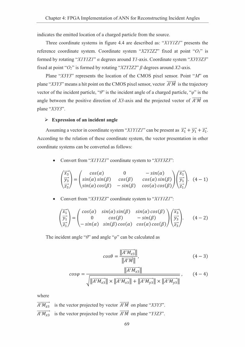
Chapter 4: FPGA Implementation of ANN for Reconstructing Incident Angles
69
indicates the emitted location of a charged particle from the source.
Three coordinate systems in figure 4.4 are described as: “X1Y1Z1” presents the
reference coordinate system. Coordinate system “X2Y2Z2” fixed at point “O1” is
formed by rotating “X1Y1Z1” α degrees around Y1-axis. Coordinate system “X3Y3Z3”
fixed at point “O2” is formed by rotating “X2Y2Z2” β degrees around X2-axis.
Plane “X3Y3” represents the location of the CMOS pixel sensor. Point “M” on
plane “X3Y3” means a hit point on the CMOS pixel sensor, vector �²Rµµµµµµµµ¶ is the trajectory
vector of the incident particle, “θ” is the incident angle of a charged particle, “φ” is the
angle between the positive direction of X3-axis and the projected vector of �²Rµµµµµµµµ¶ on
plane “X3Y3”.
Ø Expression of an incident angle
Assuming a vector in coordinate system “X1Y1Z1” can be present as KDµµµ¶ N LDµµµµ¶ N �Dµµµ¶. According to the relation of these coordinate system, the vector presentation in other
coordinate systems can be converted as follows:
· Convert from “X1Y1Z1” coordinate system to “X3Y3Z3”:
¨K2µµµµ¶L2µµµµ¶�2µµµ¶« = ¨ y}h6·9 +++++++++++++++++W+++++++++++++++++ 8 hfe6·9hfe6·9 hfe6�9++++++y}h6�9++++++++y}h6·9 hfe6�9hfe6·9 y}h6�9 ++++8 hfe6�9+++++y}h6·9 y}h6�9«¨KDµµµ¶LDµµµµ¶�Dµµµ¶«I+++6b 8 79
· Convert from “X3Y3Z3” coordinate system to “X1Y1Z1”:
¨KDµµµ¶LDµµµµ¶�Dµµµ¶« = ¨ y}h6·9++++hfe6·9 hfe6�9++++hfe6·9 y}h6�9W+++++++++++++ y}h6�9++++++++++++8 hfe6�98 hfe6·9+++hfe6�9 y}h6·9+++y}h6·9 y}h6�9«¨K2µµµµ¶L2µµµµ¶�2µµµ¶«I++++++++6b 8 J9
The incident angle “θ” and angle “φ” can be calculated as
y}h4 = ¸�²R¹2µµµµµµµµµµµµ¶¸¸�²Rµµµµµµµµ¶¸ 5+++++++++++++++++++++++++++++++++++++++++++++++++6b 8 P9 y}h� = ¸�²R<2µµµµµµµµµµµµ¶¸U¸�²R<2µµµµµµµµµµµµ¶¸ × ¸�²R<2µµµµµµµµµµµµ¶¸ N ¸�²R~2µµµµµµµµµµµµ¶¸ × ¸�²R~2µµµµµµµµµµµµ¶¸+5+++++++++6b 8 b9
where �²R¹2µµµµµµµµµµµµ¶ is the vector projected by vector �²Rµµµµµµµµ¶ on plane “X3Y3”. �²R<2µµµµµµµµµµµµ¶ is the vector projected by vector �²Rµµµµµµµµ¶ on plane “Y3Z3”.

Chapter 4: FPGA Implementation of ANN for Reconstructing Incident Angles
70
�²R~2µµµµµµµµµµµµ¶ is the vector projected by vector �²Rµµµµµµµµ¶ on plane “X3Z3”.
Ø Expression of º²»µµµµµµµµ¶ and º²»¼½µµµµµµµµµµµµ¶ The unit vector of vector �²Rµµµµµµµµ¶ in coordinate system “X1Y1Z1” is expressed as
�¶ = 6hfe6!9 y}h6`9++hfe6!9 hfe6`9++8 y}h6!99¨KDµµµ¶LDµµµµ¶�Dµµµ¶« = 6/++++0++++y9 ¨KDµµµ¶LDµµµµ¶�Dµµµ¶«5+++6b 8 o9 where
σ is the angle between �²Rµµµµµµµµ¶ and the negative direction of Z1-axis.
γ is the angle between �²Rµµµµµµµµ¶ and the positive direction of X1-axis.
�²Rµµµµµµµµ¶ is presented as
�²Rµµµµµµµµ¶ = 6/g++++0g++++yg9 ¨KDµµµ¶LDµµµµ¶�Dµµµ¶«+5++++++++++++++++++++++++++++++6b 8 Q9 where
t is the flight time of the charged particle from the emission point “A’” to the hit
point “M” on the CMOS pixel sensor.
The expression of �²Rµµµµµµµµ¶ in the coordinate system “X3Y3Z3” is derived from the
formula (4-1) and presented as
�²Rµµµµµµµµ¶ = 6K2µµµµ¶+++L2µµµµ¶+++�2µµµ¶9 ¨ /gy}h6·9 8 yghfe6·9/ghfe6·9hfe6�9+N +0gy}h6�9 +N ygy}h6·9hfe6�9/ghfe6·9y}h6�9 +8 +0ghfe6�9 +N +ygy}h6·9y}h6�9« I 6b 8 �9 The projected vector of �²Rµµµµµµµµ¶ on plane “X3Y3” is expressed as
�²R¹2µµµµµµµµµµµµ¶ = 6K2µµµµ¶+++L2µµµµ¶+++�2µµµ¶9+� WW/ghfe6·9y}h6�9 8 0ghfe6�9 N ygy}h6·9y}h6�9�I++6b 8 Y9
Ø Expression of fly time (t)
Vector R¾2µµµµµµµµµ¶ on plane “X3Y3”, and it is passed by the normal vector �2µµµµ¶. The two
vectors are perpendicular to each other. They are written as

Chapter 4: FPGA Implementation of ANN for Reconstructing Incident Angles
71
R¾2µµµµµµµµµ¶ × �2µµµµ¶ = W+I+++++++++++++++++++++++++++++++++++++++++++++6b 8 �9 According to formula (4-1), �2µµµ¶ is written as
�2µµµ¶ = ³hfe6·9y}h6�9 +++8 hfe6�9++++y}h6·9y}h6�9´¨KDµµµ¶LDµµµµ¶�Dµµµ¶«+5+++++++++++++6b 8 7W9 Vector R¾2µµµµµµµµµ¶ is calculated as follows:
¾D¾2µµµµµµµµµµ¶ = ¾D¾3µµµµµµµµµµ¶ N ¾3¾2µµµµµµµµµµ¶ = �DLDµµµµ¶ N �3K3µµµµ¶ = 6KDµµµ¶+++LDµµµµ¶+++�Dµµµ¶9¨ �3y}h6·9�D8�3hfe6·9«5+++++6b 8 779 where
O3 is the projected position of the central point “A” on plane “X3Y3”.
d1 is the distance between point “O1” and point “O2”.
d2 is the distance between point “O2” and “O3”.
¾2�µµµµµµµ¶ = + 6KDµµµ¶+++LDµµµµ¶+++�Dµµµ¶9 � WW� N �3hfe6·9�5+++++++++++++++++++++++++++++++++ 6b 8 7J9 ¾D�µµµµµµµ¶ = ¾D¾3µµµµµµµµµµ¶ N ¾3¾2µµµµµµµµµµ¶ N ¾2�µµµµµµµ¶ = ¾D¾2µµµµµµµµµµ¶ N ¾2�µµµµµµµ¶ = 6KDµµµ¶+++LDµµµµ¶+++�Dµµµ¶9 ��3y}h6·9�D� � 5 6b 8 7P9
where
D is the distance of normal vector from point “ A ” to the plane “ X1Y1 ”.
Position of “O3” projected by point “A” on plane “X3Y3” varies with the angle α
and β. However, considering “D” is large enough, the variety of d2 can make little
difference in ¾2�µµµµµµµ¶.
��¿µµµµµµ¶ = 6KDµµµ¶+++LDµµµµ¶+++�Dµµµ¶9 �Ày}h6�9Àhfe6�9W �5+++++++++++++++++++++++++++++++ 6b 8 7b9 ¾D�²µµµµµµµµµ¶ = ¾D�µµµµµµµ¶ N ��²µµµµµµµ¶ = 6KDµµµ¶+++LDµµµµ¶+++�Dµµµ¶9 ��3 y}h6·9 N Ày}h6�9�D N Àhfe6�9� �5++++++++++6b 8 7o9
where

Chapter 4: FPGA Implementation of ANN for Reconstructing Incident Angles
72
δ is the angle between the vector ��²µµµµµµµ¶ and the X1-axis.
ρ is the radius of the source.
¾DRµµµµµµµµ¶ = ¾D�²µµµµµµµµµ¶ N �²Rµµµµµµµµ¶ = 6KDµµµ¶+++LDµµµµ¶+++�Dµµµ¶9 ��3 y}h6·9 N Ày}h6�9 N /g�D N Àhfe6�9 N 0g� N yg �I+++++++6b 8 7Q9 R¾2µµµµµµµµµ¶ = ¾D¾2µµµµµµµµµµ¶ 8 ¾DRµµµµµµµµ¶ = 6KDµµµ¶+++LDµµµµ¶+++�Dµµµ¶9 ¨ 86/g N Ày}h6�99860g N Àhfe6�9986�3hfe6·9 N � N yg9«I++++++6b 8 7�9
where a, b and c in the formula is
+++++++++++++++++Á/ = hfe6�9y}h6`90 = hfe6�9hfe6`9y = 8y}h6�9+ ÂI+++++++++++++++++++++++++++++++++++++ 6b 8 7Y9 The flight time t of particles is expressed as
g = 8 ³�3y}h6!9 N Ày}h6�9´hfe6·9y}h6�98 Àhfe6�9hfe6�9 N �y}h6·9y}h6�9hfe6!9 �Ãs6`9 hfe6·9y}h6�98 hfe6!9hfe6`9hfe6�98 y}h6!9y}h6·9y}h6�9I 6b 8 7�9 Correlations between incident angle θ and angles α and β are shown in figure 4.5,
which is the simulation result based on the formula (4-3). According to the result, the
incident angle θ of raw data required can be fixed according to the angles (α, β).
Figure 4.5: Simulation result of the correlation between incident angle φ, θ and α, β.

Chapter 4: FPGA Implementation of ANN for Reconstructing Incident Angles
73
Setting
For training datasets and test datasets, 10 different incident angles were chosen to
collect raw data. Detailed information of 10 incident angles (θ) is shown in Table 4-1,
including angle φ presenting the angle between the main axis of a cluster and the
X-axis.
Table 4-1: The setting of the angle θ, φ, and α, β.
θ (deg) φ(deg) α (deg) β (deg)
0 0 0 0
15 136 -10 -10
30 90 0 -30
44 120 -20 -40
50 90 0 -50
56 127 -30 -50
62 113 -20 -60
64 124 -30 -60
71 111 -20 -70
73 127 -30 -70
In the training process, a large amount of raw data was acquired for each given
incident angle θ. In the test process, 500 frames of raw data were acquired for each
given incident angle θ.
4.1.3 Readout Chain
Figure 4.6: Schematic diagram of the MIMOSA 18 readout chain [4].
The readout chain of the raw data acquisition system is shown in figure 4.6, which
presents the transmission of raw data and control signals between PC and the
MIMOSA18.
The MIMOSA18 (“MAPS”) was mounted on a device test board which is used to

Chapter 4: FPGA Implementation of ANN for Reconstructing Incident Angles
74
provide the power supply, mechanical support and transmit control signals, such as the
clock, the reset, from an auxiliary board.
An auxiliary board is used to transmit analog data from the device test board to an
imager board. In order to reduce the data attenuation due to long-distance transportation,
the single-end signal from the device test board is amplified and converted to
differential forms on the auxiliary board. Then, the differential signal is sent to the
imager board via coaxial cables. In addition, the analog signal is sampled from the
auxiliary board and monitored on an oscilloscope.
On the imager board, analog data from the auxiliary board is digited to 12-bit and
then sent to the disk of Windows PC through an ethernet link. The imager board is set
up in and powered by a VME crate [4][5][6].
In the process of raw data acquisition, the device test board equipped with the
MIMOSA 18 chip is placed in a dark chamber. The noise level is 2.2 ADC units, which
is the average output of the chip in the dark chamber without irradiation of source 90Sr.
4.2 Implementations in the FPGA
Figure 4.7: FPGA development board (Nexys Video Artix-7 FPGA) used in our study.
A NEXYS VIDEO FPGA development board was used to implement the ANN and
preprocessing modules, as shown in figure 4.7. The development board has a Xilinx
Artix-7 XC7A200T FPGA chip [7], high-speed USB interfaces, Bank RAMs, DSP
modules and other resources.
An 8-bit micro USB interface (see "INTERFACE") was activated to read raw data
into the FPGA board and write back reconstructed information to PC frame by frame. A

Chapter 4: FPGA Implementation of ANN for Reconstructing Incident Angles
75
piece of reconstructed information contains cluster information (pixel charges and their
relative positions in a cluster window) and the corresponding incident angle θrec
reconstructed by the ANN.
Raw data read in the FPGA device is processed by Correlated Double Sampling
(CDS) firstly of all, generating pixel charges. Two switches (see "SWITCH") on the
board are called to supply alternative options on the data width of pixel charges. In my
implementation, the two switches are set as “00” for data width is original 12-bit.
Figure 4.8: Main procedures and timing in the FPGA device.
Main procedures and timing of raw data processed in the FPGA device are shown
in figure 4.8:
1. Reading one frame of raw data from PC:
256×256 pixels of 32-bit raw data are fed into the FPGA device and
processed the CDS pixel by pixel. 256×256 pixels of 12-bit pixel charges
are generated.
2. Cluster search:
Searching clusters in a frame of pixel charges. If there is a seed pixel
in this frame, neighbour pixel charges of the seed pixel are collected and
next step is started; otherwise, there is no cluster in the frame and the
procedure jumps to the last step write reconstructed results of this frame
back to PC.
3. Data format conversion:

Chapter 4: FPGA Implementation of ANN for Reconstructing Incident Angles
76
Due to the exiting of IP core in the design suit of vivado, in order to
simplify the implementation procedure in the FPGA, the integer is
converted into floating point for the main calculation in the subsequent
procedure.
4. Feature extraction:
Four features are extracted to present the cluster. The maximum and
the minimum standard deviation of a cluster are calculated in the module
named Main Component Analysis (MCA). Total charges of the cluster and
the seed pixel charge are calculated within the process of cluster search.
5. Norm input:
The four features are normalized respectively and then fed into the
ANN.
6. ANN:
An incident angle is reconstructed based on four normalized features
of the cluster and weights fitted in the training process.
7. DeNorm output:
The output of the ANN is denormalized which is the reverse process
of the normalization.
8. Write results back:
Reconstructed information (relative positions, pixel charges and the
corresponding reconstructed angle θrec) in a frame is written back to PC.
4.2.1 Interface to Read in Raw Data
Each frame of raw data is stored in binary files by the fixed format, including some
configuration contents (head part and end part). Raw data is extracted from the frame
and transferred to the FPGA device through the 8-bit micro USB interface. The frame
format of the file and the process of data reception in the FPGA are described in this
section.
Format of Raw Data
A frame of raw data (256×256 pixels) is composed of three parts as shown in figure
4.9, including the head part, the body part and the end part.
Ø The head part: It is used to indicate the start of the frame. The head part is

Chapter 4: FPGA Implementation of ANN for Reconstructing Incident Angles
77
composed of 112 bytes binary data. The number of the frame (“Num fr”) is
recorded two times from 5th byte to 12th byte as shown in figure 4.9.
Ø The body part: It is the main content of the frame. The body part contains
256×256 pixels of 32-bit raw data. Only the body part is extracted and
transported to the FPGA device. 32-bit raw data of each pixel are expressed
in three parts, including two 12 bits data and an 8-bit extra data. Two 12 bits
of raw data are two samples of one pixel, respectively, which are supplied
to the CDS module.
Ø The end part: It is used to indicate the end of a frame. The end part is
expressed in a fixed number (4 bytes). The first byte is (EF)hex, the second
byte is (CD)hex, the third byte is (AB)hex, the last byte is (89)hex.
Figure 4.9: Frame format stored in a binary file (256×256 pixels).
The principle of body part extraction is described as follows:
1. The head part is searched and verified in a binary file;
2. Then next 256×256×4 bytes raw data are read out and written into a memory of
PC.
3. Reading out the following 4 bytes, if they are the same with the end part, it
means that raw data in the memory is a complete body part and will be
transferred to the FPGA; otherwise, the memory is reset and the next head part
is searched in the binary file.
Through the frame format design (the head part and the end part), the integrity and

Chapter 4: FPGA Implementation of ANN for Reconstructing Incident Angles
78
the accuracy of raw data transmitted to the FPGA are guaranteed.
Data Reception in the FPGA
The timing waveform to read raw data of one pixel is illustrated in figure 4.10.
Relevant signals are described as follows:
Ø Prog_oen: It is an output signal of the FPGA chip and used to control the micro
USB interface to receive data. Signal “Prog_oen” needs to be active (low-level
voltage) one clock cycle before signal “prog_rdn” pulled down when raw data
starts to be transferred.
Ø Prog_rdn: It is an output signal of the FPGA chip and used to control the micro
USB interface to receive data. Raw data will be received only when signal
“Prog_oen” and signal “Prog_rdn” are both enabled (low-level voltage).
Ø Prog_clko: A 60 MHz clock signal supplied by the micro USB interface chip.
This 60 MHz clock is used as the system clock in our design.
Ø Prog_d: It is an 8-bit data bus to transport data between PC to the FPGA device.
In figure 4.10, raw data of the pixel shown is (ABCDEF00)hex, the period for
receiving is 6 clock cycles.
1st clock cycle: Reading in the first 8-bit raw data in a register.
2nd clock cycle: Reading in the second 8-bit raw data in a register.
3rd clock cycle: Reading in the third 8-bit raw data in a register.
4th clock cycle: CDS operation. The CMOS pixel sensor MIMOSA18 output
integration signals and reset signals, respectively. The two signals are voltages of the
same sampling node at different time. In the CDS module, which is achieved in the
FPGA device, the offset signal of the pixel charge is removed by subtracting the reset
signal from the integration signals. In the case of the negative number (close to number
zero) occurring by the subtraction, extra modules are needed to convert and unify the
format of the integer value. In order to reduce the complications of the implementation,
the pixel charge is limited in positive number as expressed
ÄiÅÆl+�¤��ÇÆ = �È�7 8 È�J�I++++++++++++++++++++++++++++6b 8 JW9++ The first three 8-bit raw data are two 12-bit pixel charges of Fr1 and Fr2. For the
example of the pixel shown in figure 4.10, where Fr1 is (DAB)hex, and Fr2 is (EFC) hex.

Chapter 4: FPGA Implementation of ANN for Reconstructing Incident Angles
79
The pixel charge equalling to (151)hex is stored in a memory of the FPGA chip.
5th clock cycle: The resolution of the pixel charge is adjusted. There is a 2-bit
switch that can set the resolution of the pixel charge at 4-bit, 5-bit, 8-bits and 12-bit. In
our application, the switch [1:0] is set “00” which means the resolution is 12-bit, it is
equal to the original resolution of a pixel.
6th clock cycle: Reading in the last 8-bit raw data of the pixel.
Figure 4.10: Timing waveform to read in raw data of an example from PC to the FPGA device.
4.2.2 Cluster Search
The cluster search process is used to find out clusters in the matrix of pixel charges
(12-bit). The algorithm for cluster search is described and the simulation result is
illustrated.
Algorithm for Cluster Search
Incident angles are reconstructed based on features of each cluster, including the
cluster shape and the charge distribution. The performance of the algorithm for cluster
search directly determines the reliability of reconstruction results. Parameters of the
algorithm are presented as follows:
Ø Noise threshold: It is set to 5 ADC units. The output of the CMOS pixel
without irradiation of source is about 2.2 ADC units due to the background
and some electoral noises. The threshold is set above 2×2.2 ADC to filter
the pixel charge affected by the background. A cluster is formed by some
adjacent fired pixels. If the output amplitude of a pixel is higher than the
noise threshold, it is defined as a fired pixel [8].
Ø Seed pixel: It has the largest charge in a cluster and exceeds the seed

Chapter 4: FPGA Implementation of ANN for Reconstructing Incident Angles
80
threshold. It is used to fix the initial pixel of a cluster and locate the
neighbour pixels. In the algorithm, a seed pixel is located at the central
position of a 7×7 cluster window, its relative coordinate is (3, 3).
Ø Seed threshold: It is set to equal to 12 ADC units. Seed pixels have the
largest charge in a cluster, the threshold is set above 5×2.2 ADC.
Ø Cluster window: It is a 7×7 pixels matrix which is used to limit the
maximum area of a cluster.
Figure 4.11: Incident angles of charged particles.
As shown in figure 4.11, the maximum incident angle that can be
reconstructed depends on the size of the cluster window. It is calculated as
g/e4�%< = eda × 1fgyÉS1f +5+++++++++++++++++++++++++++ 6b 8 J79 where
pitch is the pixel pitch of the CMOS pixel sensor (10 µm).
epi is the thickness of the epitaxial layer (14 µm).
num is the number of pixels in the horizontal or vertical direction of
the cluster window. It equals 7 for the 7×7 cluster window.
According to formula (4-21), the largest value of the reconstructed
angle θrec is 78.6 degrees. For a 5×5 cluster window, θrec is 74.35 degrees.
According to the setting of the raw data acquisition system, the maximum
incident angle is 73 degrees. Considering the deviation of incident angles
that can be generated during the acquisition process, the 7×7 cluster
window is chosen in the feasibility study. It means that a cluster shape
which is larger than 7×7 cluster window will be recognized as two or more
clusters.

Chapter 4: FPGA Implementation of ANN for Reconstructing Incident Angles
81
Steps of the algorithm for cluster search in the FPGA device are shown in figure
4.12 and described as follows:
Figure 4.12: Algorithm for cluster search implemented in the FPGA device.
1. Reading a 256×256 matrix of pixel charges
Read in a 256×256 matrix of 12-bit pixel charges from the interface register and
store in the memory of the FPGA.
2. Adding 0 around the matrix
To collect a complete cluster, neighbour pixels around a seed pixel need to be
checked. Charges of neighbour pixels are extracted from the matrix according to their
addresses. If the seed pixel is located at the boundary column, addresses of neighbour
pixels on some directions are illegal. In order to avoid the illegal address, four
exceptional options need to be set for the seed pixel located at boundary columns (left,
right, top and bottom) to stop the algorithm on the direction.
Number 0 is added around the matrix to reduce the complexity of the algorithm on
the boundary column. For instance, a seed pixel is located at the left boundary column.
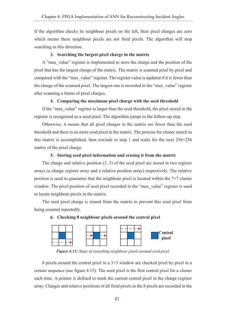
Chapter 4: FPGA Implementation of ANN for Reconstructing Incident Angles
82
If the algorithm checks its neighbour pixels on the left, their pixel charges are zero
which means these neighbour pixels are not fired pixels. The algorithm will stop
searching in this direction.
3. Searching the largest pixel charge in the matrix
A “max_value” register is implemented to store the charge and the position of the
pixel that has the largest charge of the matrix. The matrix is scanned pixel by pixel and
compared with the “max_value” register. The register value is updated if it is fewer than
the charge of the scanned pixel. The largest one is recorded in the “max_value” register
after scanning a frame of pixel charges.
4. Comparing the maximum pixel charge with the seed threshold
If the “max_value” register is larger than the seed threshold, the pixel stored in the
register is recognized as a seed pixel. The algorithm jumps to the follow-up step.
Otherwise, it means that all pixel charges in the matrix are fewer than the seed
threshold and there is no more seed pixel in the matrix. The process for cluster search in
this matrix is accomplished, then rewinds to step 1 and waits for the next 256×256
matrix of the pixel charge.
5. Storing seed pixel information and erasing it from the matrix
The charge and relative position (3, 3) of the seed pixel are stored in two register
arrays (a charge register array and a relative position array) respectively. The relative
position is used to guarantee that the neighbour pixel is located within the 7×7 cluster
window. The pixel position of seed pixel recorded in the “max_value” register is used
to locate neighbour pixels in the matrix.
The seed pixel charge is erased from the matrix to prevent this seed pixel from
being counted repeatedly.
6. Checking 8 neighbour pixels around the central pixel
Figure 4.13: Steps of searching neighbour pixels around seed pixel.
8 pixels around the central pixel in a 3×3 window are checked pixel by pixel in a
certain sequence (see figure 4.13). The seed pixel is the first central pixel for a cluster
each time. A pointer is defined to mark the current central pixel in the charge register
array. Charges and relative positions of all fired pixels in the 8 pixels are recorded in the

Chapter 4: FPGA Implementation of ANN for Reconstructing Incident Angles
83
two register arrays respectively. Then the algorithm leaps to step 7.
Steps to check one neighbour pixel are described in step 6.1, 6.2, 6.3.
6.1 Checking the relative position of the neighbour pixel
If the relative position of the neighbour pixel both on X-axis and Y-axis
are in the range of [0, 6], it means that the neighbour pixel is located
within the area of the 7×7 cluster window. The algorithm continues to
the next step.
Otherwise, the neighbour pixel is out of the cluster window and it is not
a part of the cluster. The algorithm returns to step 6 to calculate the
relative position of the next neighbour pixel.
6.2 Checking the charge of the neighbour pixel
If the neighbour pixel charge is larger than the noise threshold, it is a
fired pixel. The algorithm continues to the next step.
Otherwise, the neighbour pixel is not a fired pixel. The algorithm
returns to step 6 to calculate the relative position of the next neighbour
pixel.
6.3 Storing neighbour pixel information and erasing it from the
matrix.
The pixel charge and the relative position of the neighbour pixel are
stored in the two register arrays respectively. Then erase the charge of
the neighbour pixel from the matrix to prevent it from being counted
repeatedly.
7. Checking the charge register array
It is used to check whether the search process for the cluster is accomplished. After
8 neighbour pixels are scanned, the current central pixel pointer is moved to the next
register of the charge register array. If the register is not empty, it means that there is a
fired pixel in the 8 neighbour pixels which is chosen as the next central pixel. Then the
algorithm returns to step 6 to check 8 neighbour pixels around the new central pixel.
If the register is empty, it means that all fired pixels adjacent to the seed pixel have
been recorded and the algorithm stops for this seed pixel. Pixel charges and relative
positions stored in the two register arrays are transferred to an output bank RAM. Then
the two register arrays are reset. The algorithm leaps to step 3 to find the next seed pixel
in the matrix.

Chapter 4: FPGA Implementation of ANN for Reconstructing Incident Angles
84
Simulation Results
Besides the algorithm with the 7×7 cluster window described before, the algorithm
without cluster window and the algorithm with the 5×5 cluster window are all achieved
by C code. 500 frames of raw data for each given incident angle (Table 4.1) are taken to
test these algorithms. Test results are shown in figure 4.14, where cluster counts are the
number of clusters found for each given incident angle.
Figure 4.14: Cluster counts found by algorithms with different cluster windows.
The algorithm without cluster window means that there is no limitation for the size
of a cluster. A cluster is identified only based on the connectivity between fired pixels
and the seed pixel. For instance, a cluster shape that presents an elongated strip shape,
even if more than 7 pixels, is defined as one cluster. Cluster counts found by the
algorithm are the least among the three algorithms.
For the algorithm with a cluster window, the size limitation of a cluster is
considered in addition to the connectivity of fired pixels and the seed pixel. The
algorithm with the 5×5 cluster window limits the size of a cluster within 5×5 pixels.
Cluster counts found by this algorithm are the most among the three algorithms.
As shown in the test result, cluster counts found by the algorithm with the 7×7
cluster window make a balance between the other two algorithms.

Chapter 4: FPGA Implementation of ANN for Reconstructing Incident Angles
85
Figure 4.15: Cluster counts of an elongated cluster found by the three algorithms.
Comparing with clusters identified by the algorithm without cluster window, the
limitation on the size of a cluster can divide one large cluster into two or more clusters.
And with the decrease in the size of the cluster window, more clusters are recognized.
For example, there is an elongated cluster which is composed of 8 pixels as shown in
figure 4.15. 3 clusters are identified by the algorithm with the 5×5 cluster window, 2
clusters are recognized by the 7×7 cluster window, however, only one cluster is
recorded by the algorithm without a cluster window.
As shown in figure 4.14, the number of elongated clusters increases as the incident
angle increases, leading to the gap on cluster counts by the three algorithms expands.
Taking account in the common cluster size and incident angles, the algorithm with the
7×7 cluster window is implemented in the FPGA device.
Figure 4.16: Simulation of cluster counts and effective surface.
In the raw data acquisition system, the incident angle is altered by tuned the angle
between the MIMOSA 18 and the reference plane. The effective surface of the chip
means the size of chip projected on the flat reference plane. The effective detection
surface of MIMOSA 18 has some variation for different incident angles (see formula

Chapter 4: FPGA Implementation of ANN for Reconstructing Incident Angles
86
4-22), resulting in a change in the number of incident particles that can be collected.
The cluster count presents the same trend as the effective surface decreases. However,
the sharp increase of cluster counts occurs in figure 4.16, as marked point A at incident
angle θinc = 50 degrees. Firstly, because of the reflection of the support below the chip,
one particle may re-entrance the sensor again to generate extra clusters. Secondly, due
to components around the chip, angle α make the larger influence on the cluster counts
than angle β.
S��Sygf^S+hd|�/ySyÉf1+hd|�/yS = y}h6·9 × y}h6�9I++++++++++++++++++++++6b 8 JJ9 4.2.3 Data Format Conversion
In units following the cluster search module, operands are in the floating-point
format, such as trigonometric function values supplied for feature extraction, and
weights of the ANN. The 12-bit integer of the pixel charge has to be converted to the
floating-point format to ensure a consistent data format. The floating-point
conversation may lead some reduction on the data accuracy. However, firstly,
convenience of implementation. conversion IP cores are existed which can be used for
converting the integer into floating-point. Secondly, the feasibility study try to provide
the proof of the principle that tag particles according to the incident angle based on the
ANN has been established.
Single-precision floating-point format (binary 32) is one format of the IEEE 754
standard, which is a binary number format standard used in many hardware
floating-point units [9][10].
Figure 4.17: Format of Single-precision floating-point [10].
As shown in figure 4.17, the value expressed in the single-precision floating-point
format can be calculated as
^/�dS = 6879Ê × J6>HD3Ë9 × 67 N h19 ++++++++++++++++++++++++++++++++6b 8 JP9 where

Chapter 4: FPGA Implementation of ANN for Reconstructing Incident Angles
87
h6hfme9 = 02D+I+++++++++++++++++++++++++++++++++++++++++++++++++++++6b 8 Jb9 S6SK1}eSeg9 = �³0( × J(H32´2�
(�32 I++++++++++++++++++++++++++++++ 6b 8 Jo9 h16Ìfmef�fy/e�+1|Syfhf}e9 =�³0( × J(H32´+I33
(�� ++++++++++++++6b 8 JQ9 An Intellectual Property (IP) core is called in the FPGA device to convert the 12-bit
integer pixel charge to IEEE 754 single-precision floating-point format.
4.2.4 Feature Extraction
Clusters have various expressions on the shape and the charge distribution,
depending on different incident angles of charged particles. In order to achieve accurate
incident angle reconstruction as much as possible, and taking into account the
complexity of the artificial neural network structure, four features of a cluster are
chosen and fed into the ANN structure, that is total charges of fired pixels (Totchar), the
charge of the seed pixel (SeedChar), the maximum and the minimum standard
deviation (MaxStd and MinStd) of the cluster.
Total Charges of Fired Pixels
Totchar is the sum of all fired pixel charges of a cluster which is related to the
incident angle. It is determined by the distance of an incident particle in the epitaxial
layer. The larger the incident angle of a charged particle, the longer it moves in the
epitaxial layer and the more pixels are affected.
The average energy loss of charged particles when they pass through matter is
described by the Bethe-Bloch formula (see chapter 1). Fluctuations of the energy loss in
a thin absorber are described by Landau in 1944 [11]. The number of electron-hole
pairs is related to the energy loss (Δ) in the matter. In figure 4.18, energy loss
distributions for 500 MeV pions incident on thin a silicon detector is presented, where
f(x, Δ) represents the distribution probability of the energy loss (Δ) when an incident
particle traverses a layer of matter with thickness x. As fluctuations of the energy loss in
a thin layer are large, the incident angle is not absolutely proportional to the total charge
of a cluster. Incident angles cannot be reconstructed only based on the total charge.

Chapter 4: FPGA Implementation of ANN for Reconstructing Incident Angles
88
Figure 4.18: Stopping power for positive muons in cupper Straggling functions in silicon for
500MeV pions, normalized to unity at the most probable value Δp/x [12].
The Charge of the Seed Pixel
SeedChar is the pixel charge of the seed pixel of a cluster. It represents the largest
number of electrons attracted in the epitaxial layer by a collection diode. The feature is
related to the incident angle.
Maximum Standard Deviation (Minimum Standard Deviation)
As shown in figure 4.19, the particle hit on the CPS with an incident angle θ and
generate a cluster, the angle between the main axis of the cluster and the X-axis is angle
φ. MaxStd is the standard deviation along the main axis of the cluster, and MinStd is
calculated along the vertical direction of the main axis. These two features are affected
by the incident angle and reflect the shape and charge distribution of a cluster. An
individual unit named Main Component Analysis (MCA) is designed to calculated
MaxStd and MinStd.
Figure 4.19: The main axis of a cluster.
Ø The variance of a cluster along X-axis and Y-axis

Chapter 4: FPGA Implementation of ANN for Reconstructing Incident Angles
89
For a random variable K which is discrete with probability mass function kD Í1D5 k3 Í 135 ÎÎ 5 k( Í 1( . pi is the probability of ki. The variance of the random
variable K can be calculated as
T/|6Ï9 =�1(6k( 8 �93 = 6�1(k(39 8 �3)(�D +5+++++++++��1()
D = 7�5++++++++++6b 8 J�9)(�D
where
µ is the expected value of the random variable k, it is presented as
� = +�1(k(+)(�D I+++++++++++++++++++++++++++++++++++++++++ 6b 8 JY9
In a cluster, positions of fired pixels are discrete with probability mass function KD Í ÐÑÐÒ 5 K3 Í ÐÓÐÒ 5 ÎÎ 5 K( Í ÐÔÐÒ. Qi is the pixel charge of fired pixel i Qt is the total
pixel charge of all fired pixels in the cluster. The variance of the cluster along X-axis
can be calculated as
T/|6V9 = ÕV3Ö 8 ÕVÖ3 =�vK(3 × Ø(Ø#z)(�D 8 ��K( × Ø(Ø#
)(�D �3 5�Ø(Ø#
)(�� = 75 6b 8 J�9
where
ÕV3Ö = �K(3 × Ø()(�D Ø#Ù I+++++++++++++++++++++++++++++++++++++++ 6b 8 PW9
ÕVÖ = � =�K( × Ø()(�D Ø#Ù I+++++++++++++++++++++++++++++++++++++ 6b 8 P79!
The variance of the cluster along Y-axis is expressed as
T/|6¥9 = Õ¥3Ö 8 Õ¥Ö3 =�vL(3 × Ø(Ø#z)(�D 8 ��L( × Ø(Ø#
)(�D �3 5�Ø(Ø#
)(�� = 7I+++6b 8 PJ9
where
n is the number of fired pixels in a cluster.
xi is the distance along X-axis between the position of the fired pixel i the original

Chapter 4: FPGA Implementation of ANN for Reconstructing Incident Angles
90
point.
yi is the distance along Y-axis between the position of the fired pixel i the original
point.
xi and yi are calculated as
ÚK( = ³K@AÊ(#(A) N WIo´ × 1fgyÉ<L( = ³L@AÊ(#(A) N WIo´ × 1fgyÉ~Û+5++++++++++++++++++++++++ 6b 8 PP9!where
xposition is the relative position of a pixel in the 7×7 cluster window along X-axis.
yposition is the relative position of a pixel in the 7×7 cluster window along Y-axis.
0.5 is the half-pixel between the original point and the centre of the first pixel.
pitchx is the distance between two neighbour pixels along the X-axis, it is 10 µm for
CMOS pixel sensor MIMOSA 18.
pitchy is the distance between two neighbour pixels along the Y-axis, it is 10 µm for
CMOS pixel sensor MIMOSA 18.
As shown in figure 4.20, xi and yi of a point “M” can be calculated in the following
way. The relative position of point “M” in the cluster window (xposition, yposition) is (3,1).
The distance (xi) along X-axis between the position of the pixel to the original point is
35 µm, yi is 15 µm along Y-axis
Figure 4.20: Position of a fired pixel in a cluster.
Ø Maximum and minimum standard deviation of a cluster
As shown in figure 4.21, the vector ¾Rµµµµµµ¶ in reference coordinate system can be
obtained as

Chapter 4: FPGA Implementation of ANN for Reconstructing Incident Angles
91
¾Rµµµµµµ¶ = K × K¶ N L × L¶+ +++++++++++++++++++++++++++++++++++++++6b 8 Pb9
where x and y are positions of point “M” in the reference coordinate system
respectively.
The vector ¾Rµµµµµµ¶ can be presented as
¾Rµµµµµµ¶ = K² × K²µµµ¶ N L² × L²µµµ¶+5+++++++++++++++++++++++++++++++++++++++++6b 8 Po9 where the K²µµµ¶ and L²µµµ¶+ are axes of a new coordinate system which is formed by rotating
α degrees from the reference coordinate system. x’ and y’ are positions of point “M”
point along X’-axis and Y’-axis in the new coordinate system, respectively.
Figure 4.21: Correlation between two coordinate systems.
The position of point M in the new coordinate system can be presented as
� K² = K × y}h6·9 N L × hfe6·9L² = 8K × hfe6·9 N L × y}h6·9¡+I+++++++++++++++++++++++++++ 6b 8 PQ9 The variance of the cluster along the X’-axis and Y’-axis can be presented as
T/|6V²9 = + ÕV²3Ö 8 ÕV²Ö3+5+++++++++++++++++++++++++++++++++++++++6b 8 P�9 T/|6¥²9 = Õ¥²3Ö 8 Õ¥²Ö3+5++++++++++++++++++++++++++++++++++++++++6b 8 PY9 where
ÕV²Ö = Ü 6K(² × Ø(9)(�D Ø# = y}h6·9 × ÕVÖ N hfe6·9 × Õ¥ÖI+++++++++++++++++++++++++++++++++++++++6b 8 P�9 ÕV²3Ö = Ü ³K(²3 × Ø(´)(�D Ø# = y}h36·9 ÕV3Ö N hfe36·9Õ¥3Ö N hfe6J·9 ÕV¥ÖI+++++6b 8 bW9

Chapter 4: FPGA Implementation of ANN for Reconstructing Incident Angles
92
Õ¥²Ö = Ü 6L(² × Ø(9)(�D Ø# = 8hfe6·9 × ÕVÖ N y}h6·9 × Õ¥Ö++I++++++++++++++++++++++++++++++++++6b 8 b79 Õ¥²3Ö = Ü ³L(²3 × Ø(´)(�D Ø# = hfe36·9 ÕV3Ö N y}h36·9Õ¥3Ö 8 hfe6J·9 ÕV¥ÖI++++6b 8 bJ9
Variances of the cluster along X’-axis and Y’-axis are functions about angle α,
which can be described as
T/|6V²9 = + ÕV²3Ö 8 ÕV²Ö3 = �<Ý6·9 = J y}h6·9 hfe6·9 6ÕV¥Ö 8 ÕVÖÕ¥Ö9 N y}h36·9 × T/|6V9 N hfe36·9 × T/|6¥9+5 6b 8 bP9 T/|6¥²9 = + Õ¥²3Ö 8 Õ¥²Ö3 = �~Ý6·9 = J y}h6·9 hfe6·9 6ÕVÖÕ¥Ö 8 ÕV¥Ö9 N hfe36·9 × T/|6V9 N y}h36·9 × T/|6¥9+I 6b 8 bb9
β is the angle that generates the maximum variance and indicates the main axis of
the cluster. β is presented as
�<Ý6�9 = Þ�ų�<Ý6·9´+I++++++++++++++++++++++++++++++++ 6b 8 bo9 Consider the resource in the hardware, it is challenging to calculate the exact angle
β and main axis of the cluster. The lookup table method is a competitive candidate for
finding the maximum or minimum value, especially for the complex calculation.
For the MCA achieved by C code in the training process, angle β can be calculated
by the inverse trigonometric function. In our design implemented in the FPGA device,
the value of trigonometric functions is stored in a lookup table, the maximum variance
is found by sweeping angles α ([0,180 degrees]) in a step of 10 degrees. The lookup
table with a step of 10 degrees reduces the accuracy of features and make a little
influence on the reconstruction result.
MaxStd and MinStd are generated as
R/KÌg� = M�<Ý6ß9+++I+++++++++++++++++++++++++++++++++6b 8 bQ9 RfeÌg� = U�~Ý6ß9+++I+++++++++++++++++++++++++++++++++6b 8 b�9

Chapter 4: FPGA Implementation of ANN for Reconstructing Incident Angles
93
4.2.5 Normalized Features
Data normalization is a fundamental preprocessing step for data mining and
machine learning [13]. It is used to remove biases among dimensions of the data vectors,
make every feature have the same weight level, and avoid large difference among
feature values. In addition, the range of the data needs to match the activation function
used in the ANN. The output range of the activation function is [-1, 1]. The function for
feature values normalization is expressed as
afe6K(9 à K( à a/K6K(9+5+++++++++++++++++++++++++++++++++++++6b 8 bY9 87 à K( 8Þin6K(9a/K6K(9 8 afe6K(9 × J 8 7 à 75++++++++++++++++++++++++6b 8 b�9
where
xi is the input feature i,
min(xi) is the minimum value of the input feature supplied by the training procedure.
max(xi) is the maximum value of the input feature supplied by the training procedure.
4.2.6 ANN Implementation
A typical one hidden layer Multi-Layer Perceptron (MLP) is implemented in the
FPGA device to reconstruct incident angles.
MLP Structure
The MLP structure contains three layers (input layer, hidden layer and output layer),
as shown in figure 4.22.
Figure 4.22: Structure of the artificial neural network.

Chapter 4: FPGA Implementation of ANN for Reconstructing Incident Angles
94
Input layer contains four input neurons and one bias neuron. Input neurons are used
to take four normalization features (Norm_SeedChar, Norm_TotChar, Norm_MaxStd
and Norm_MinStd) extracted from each cluster into the network. The value of the bias
neuron in the input layer is 1, which is used to shift the activation function.
In the hidden layer, there are 14 hidden neurons and one bias neuron. The number
of hidden neurons is determined by the training procedure in the TMVA. It is an
optimization result that takes into account resources and reconstruction efficiency. The
bias value in the hidden layer is 1. As shown in figure 4.22, there are two steps to
calculate the output of a hidden neuron:
1st step: Calculating values of summing junctions.
Input neurons including the bias neuron, are multiplied with
corresponding weights, then add all the results together. The process is
written as
�( =�K' × �'('�áD N 0D × ��D(+5++++++++++++++++++++++++++++++++6b 8 oW9
where
Ai is the result of the summing junction of hidden neuron i.
xk is the feature of input neuron k.
wki is the weight between input neuron k and hidden neuron i.
b1 is the bias neuron in the input layer, it is set as 1.
wb1i is the weight between the bias neuron in the input layer and
hidden neuron i.
2nd step: Calculating outputs of hidden neurons.
Results of summing junctions are processed by an activation function.
The procedure and the activation function (hyperbolic tangent function) are
written as
L( = �6�(9+5++++++++++++++++++++++++++++++++++++++++++++++++++6b 8 o79 �6K9 = ��n¤6K9 = S< 8 KH<S< N SH< +5+++++++++++++++++++++++++++++ 6b 8 oJ9 where
yi is the value of hidden neuron i.
f(x) is the activation funciton. The output range of the hyperbolic
tangent function is [-1,1] [14].

Chapter 4: FPGA Implementation of ANN for Reconstructing Incident Angles
95
The output layer composed of one output neuron gives the reconstructed result.
Values of all hidden neurons, including the bias neuron in the hidden layer, are
multiplied with the corresponding weights; and then added together. In our design,
there is no activation function for the output neuron. The process is expressed as
L$>Êâ?# =+ � L( × �((�DáD N 03 ×��3+5+++++++++++++++++++++6b 8 oP9
where
yresult is the output of the output neuron.
yi is the output of hidden neuron i.
wi is the weight between hidden neuron i and the output neuron.
b2 is the bias neuron in the hidden layer. It is set as 1.
wb2 is the weight between the bias neuron in the hidden layer and the output
neuron.
The MLP structure contains a total of 21 neurons and 85 weights. All weights of
the network are supplied by the training procedure performed by the TMVA.
Circuit implementation
The circuit implementation of the MLP structure is shown in figure 4.23. IP cores
and hardware resources in the FPGA device are used. Description of main modules and
signals are as follows:
Figure 4.23: Digital circuit of the artificial neural network.
Ø Sys_clk: It is the 60MHz system clock supplied by the Micro-USB
interface chip.
Ø ROM1: It is a memory module. ROM1 is used to store 14×5 weights

Chapter 4: FPGA Implementation of ANN for Reconstructing Incident Angles
96
between input neurons and hidden neurons. Weights are output from the
ROM1 according to the address supplied by an address signal. Weights
between 5 input neurons and 1 hidden neuron are output each time.
Ø Multiplier array: It is composed of 5 floating-point multiplier IP cores.
Input neurons are multiplied corresponding weights in this module. It is
controlled by the enabled signal and the system clock.
Ø Sum_1: It is an adder. The sum_1 module is used to add 5 results of the
multiplier array together. The result of one summing junction is calculated
each time in the module.
Ø f(x): It is the activation function module which is implemented by some
complex mathematic IP cores, including exponent units, sum units and
subtractor units.
Ø Register array: It is composed of 15 registers. The register array is used to
store the values of neurons in the hidden layer, including 14 hidden neurons
and the bias neuron.
Ø ROM2: It is a memory module. ROM2 is used to store 15 weights between
hidden neurons and the output neuron. One weight is output from the
ROM2 each time according to an address signal.
Ø Multiplier_output: It is a floating-point multiplier IP core.
Multiplier_output is used to multiply the output of a hidden neuron by its
weight between it and the output neuron.
Ø Sum_2: It is an adder. Sum_2 is used to add 15 outputs of the
multiplier_output unit together.
4.2.7 DeNormalized Module
The output result from the network needs to be translated into an incident angle.
DeNormalized module is used to accomplish the inverse process of the normalization
step. It is expressed as
87 à e}|a¥$>Êâ?# à 7++++++++++++++++++++++++++++++++++++++6b 8 ob9 ¥$>Êâ?# = e}|a¥$>Êâ?# N 7J 6¥$>Êâ?#�%< 8 ¥$>âÊ?#�()9 N ¥$>Êâ?#�()++++6b 8 oo9
where

Chapter 4: FPGA Implementation of ANN for Reconstructing Incident Angles
97
normYresult is the value of the output neuron.
Yresult is the degrees of the incident angle after translation.
Yresultmax is the maximum degree of the incident angle (73 degrees).
Yresultmin is the minimum degrees of the incident angle (0 degrees).
4.2.8 Interface to Output
Reconstructed information, containing cluster information (relative position and
pixel charge) and the reconstructed incident angle, is transported from the FPGA device
through the 8-bit micro USB interface to PC. The format of reconstructed information
and the transmission timing sequence are described, respectively.
Format of reconstructed information
The software developed on Windows receives and extracts the reconstructed data
according to the format. An example of the reconstructed information format is shown
in figure 4.24. It is composed of 4 parts.
Figure 4.24: Reconstructed information format of a cluster.
Ø Cluster information: It shows parameters of fired pixels that constitute the
cluster. Each fired pixel is expressed in 24-bit binary data, including the
pixel charge (16-bit) and the relative position (8-bit).
Ø Flag position 1: The number of fired pixels in each cluster is uncertain, a
flag is set to indicate the end of cluster information. Flag position 1 is
composed of 16 bits of data, expressing as (FFFF)hex.
Ø The incident angle of a cluster: It is the incident angle reconstruct by the
ANN. It is expressed in the format of single-precision floating-point and
composed of 32-bit data.

Chapter 4: FPGA Implementation of ANN for Reconstructing Incident Angles
98
Ø Flag position 2: It is used to indicate the end of a piece of reconstructed
information. It is composed of 24-bit data, expressing as (F0F0F0)hex.
Transmission timing sequence
In the FPGA device, a 24-bit bank memory is used to store reconstructed
information of one frame. The transmission timing sequence of one memory cell from
the FPGA to PC is shown in figure 4.25. Signals are illustrated as follows:
Ø Prog_wrn: It is an output signal of the FPGA chip and used to control the
process of reconstructed information transmission from the micro USB
interface to PC, which will begin when the signal is low-level voltage.
Ø MEM_en: It is an output signal of the FPGA chip and used to control the
output memory. Address of the memory cell will be locked and the data in a
memory cell will be prepared when MEM_en is low-level voltage.
Ø Prog_clko: It is the 60 MHz clock and supplied by the micro USB interface
chip.
Ø Prog_d: It is an 8-bit data signal to transport data from the FPGA device to
PC.
Figure 4.25: Timing of transporting the output result of one memory cell.
As shown in figure 4.25, 7 clock cycles are needed to transfer data of one output
memory cell (3-byte).
1st clock cycle: Signal MEM_en is enabled to locate the address of the output
memory cell, indicating the start of reading out one memory cell result.
2nd - 4th clock cycle: Three clock cycles are used to prepare the data of the output
memory cell.
5th clock cycle: The signal prog_wrn is enabled and the signal prog_d starts to
output the first byte data. The second byte and the third byte data is output continually

Chapter 4: FPGA Implementation of ANN for Reconstructing Incident Angles
99
in the 6th and 7th clock cycle.
4.3 Test results
Reconstructed results are stored in PC as binary files. Cluster information and
reconstructed incident angles are extracted and converted as the text file by the software
designed based on Windows PC. Figure 4.26 shows reconstructed results of a frame of
raw data which was taken under the incident angle of 15 degrees.
The content of the reconstructed result is shown in figure 4.26 (a). The blue part is
cluster information. The charge (“charge”) and the relative position (“position”) of a
fired pixel are presented in each line. “IEEE 754 result” is the original expression of the
reconstructed angle in the format of single-precision floating-point. “Float result” is the
degree of the incident angle converted from the “IEEE 754 result” by the software.
The reconstructed incident angles of the two clusters are 43.75 degrees and 36.41
degrees, respectively. These two clusters shapes and reconstructed results have been
validated by results reconstructed by the ANN implemented in the TMVA.
(b)
(a) (c)
Figure 4.26: Reconstructed results of a frame of raw data (a) The content of reconstructed
results (b) First cluster shape (c) Second cluster shape.

Chapter 4: FPGA Implementation of ANN for Reconstructing Incident Angles
100
4.3.1 Analysis and Discussion
500 frames of raw data for each given incident angle were collected to test the
ANN implemented in the FPGA device. The raw data was also fed into the ANN
implemented in the TMVA to produce and provide the reference result.
Figure 4.27: Difference between the mean value of reconstructed angles and the incident
angle.
The difference between the mean value of reconstructed angles 4$>&ããããã and the
incident angle θinc (see formula (4-56)) is shown in figure 4.27, where the reconstructed
angle generated by the ANN implemented in the FPGA is expressed in red and
generated by the ANN implemented in the TMVA is plotted in blue.
4$>&ããããã 8 4()& = 7e�64$>&(9 8 4()&)(�D +5++++++++++++++++++++++++6b 8 oQ9
where
n is the cluster counts of 500 frames for a given incident angle θinc. 4$>&( is the reconstructed angle of cluster i.
It can be found that angles reconstructed by two methodologies basically have the
same mean value, which indicates that the ANN implemented in the software has been
transplanted into the FPGA device. However, they are not identical and the result from
the FPGA device present high-level value on the standard deviation. It is contributed by
various reasons. For example, the data accuracy in the intermediate procedure of the
FPGA device is not matched with the software. For the MCA module of the FPGA
device, considering the resource and timing, the maximum standard deviation is

Chapter 4: FPGA Implementation of ANN for Reconstructing Incident Angles
101
searched by rotating the angle φ at a step of 10 degrees, while in the TMVA, a relatively
accurate value can be calculated by complex mathematical functions.
However, the difference between 4$>&ããããã and θinc both for the FPGA and for the
TMVA have not yet reached a precise level to make it possible to predict the real
incident angle. Ideally, the difference between 4$>&ããããã and the incident angle θinc should
float near the X-axis (y=0). Firstly, the ANN structure needs to be trained by more raw
data to optimize the number of hidden neurons. Then, four features used in the thesis
may not be enough to present cluster information related to the incident angle. For
example, replenishing a feature of the pixel number in the main axis. Finally, structures
of the CPS can be optimized, such as the pixel pitch. With the decrease of the pixel
pitch, the pixel density and resolution will be improved, differences among clusters
generated particles with different incident angles will be easier and reconstructed
results will be more accurate.
Figure 4.28: Distribution of reconstructed angles θrec versus incident angles θinc.
The distribution of reconstructed angles θrec by the ANN implemented in the FPGA
device is shown in figure 4.28. As the incident angle θinc increases, the percentage of
reconstructed angles θrec between 60 to 90 degrees increases and the percentage of
reconstructed angles θrec between 30 to 50 degrees decreases.
The range of effective reconstructed angles that we concern is from 50 to 75
degrees. Firstly, cluster shapes generated by particles with incident angles below 50
degrees do not vary obviously. In addition, these incident angles can be directly
reconstructed from hits information of a double-sided ladder [15]. On the other hand,
due to the limitation of the 7×7 window, the ANN inputs extracted from the cluster
exhibits similar features if the incident angle is above 78 degrees.

Chapter 4: FPGA Implementation of ANN for Reconstructing Incident Angles
102
The percentage of large reconstructed angles increases and the percentage of small
reconstructed angles decreases, as the incident angle increases. The variation of
reconstructed angles has the same trend as that of incident angles. Before the
optimization, the ANN cannot achieve reconstructing every high-precise incident angle,
while significantly different distributions can be found in the figure.
4.4 Summary
The feasibility study for CMOS pixel sensors with on-chip artificial neuron
networks was validated by an offline methodology.
An independent raw data acquisition system was established for hit information
collection under different incident angles (total 10 incident angles). 500 frames were
sampled for each given incident angle to test the performance of the ANN implemented
in the FPGA device.
A FPGA development board was employed for the implementation of the
preprocessing modules and the ANN. Main modules implemented in the FPGA device
were described in detail. These modules will be improved for achieving into a CMOS
pixel sensor. For example, the floating-point leads to some loss on data accuracy, the
algorithm for cluster search implemented in the FPGA device occupy large resource
and low efficiency, the feature extraction module can be achieved by some operators.
Reconstructed results by the FPGA device have been validated by result
reconstructed by the ANN implemented in the TMVA. The feasibility study
implemented in the FPGA provides the proof of the principle that tag particles
according to the incident angle based on the ANN has been established. Even though
the ANN did not achieve high-precise reconstruction as shown, reconstructed results
present obvious same trend as the variety of incident angles. With the optimization of
the ANN structure and more training processes, the performance of the ANN will be
improved. Meanwhile, the decrease of the pixel pitch in fabrication will make the gap
of the clusters generated by particles with different incident angles expand, leading to
the precision improvement of the ANN.

Chapter 4: FPGA Implementation of ANN for Reconstructing Incident Angles
103
4.5 Bibliography
[1]. Hoecker, Andreas, et al. "TMVA-Toolkit for multivariate data analysis." arXiv preprint
physics/0703039 (2007).
[2]. IPHC, "Test preliminaire de mimosa18"
[3]. Dulinski, Wojciech, et al. "Beam telescope for medium energy particles based on thin,
submicron precision MAPS." 2007 IEEE Nuclear Science Symposium Conference
Record. Vol. 2. IEEE, 2007.
[4]. Maczewski, Lukasz. "Measurements and simulations of MAPS (Monolithic Active Pixel
Sensors) response to charged particles-a study towards a vertex detector at the ILC." arXiv
preprint arXiv:1005.3710 (2010).
[5]. Koziel, Michal. Development of radiation hardened pixel sensors for charged particle
detection. Diss. Strasbourg, IPHC, 2011.
[6]. Claus, G., et al. "A portable system for monolithic active pixel sensors
characterization." IEEE Symposium Conference Record Nuclear Science 2004. Vol. 3.
IEEE, 2004.
[7]. https://store.digilentinc.com/nexys-video-artix-7-fpga-trainer-board-for-multimedia-appli
cations/
[8]. Jansen, Hendrik, et al. "Performance of the EUDET-type beam telescopes." EPJ
Techniques and instrumentation 3.1 (2016): 7.
[9]. Kahan, William. "IEEE standard 754 for binary floating-point arithmetic." Lecture Notes
on the Status of IEEE 754.94720-1776 (1996): 11.
[10]. https://en.wikipedia.org/wiki/Single-precision_floating-point_format
[11]. Landau, Lev Davidovich. "On the energy loss of fast particles by ionization." J. Phys. 8
(1944): 201-205.
[12]. http://meroli.web.cern.ch/Lecture_StragglingFunction.html
[13]. Ogasawara, Eduardo, et al. "Adaptive normalization: A novel data normalization
approach for non-stationary time series." The 2010 International Joint Conference on
Neural Networks (IJCNN). IEEE, 2010.
[14]. Manohar, T. Gowri, and VC Veera Reddy. "Load forecasting by a novel technique using
ANN." ARPN Journal of Engineering and Applied Sciences 3.2 (2008): 19-25.

Chapter 4: FPGA Implementation of ANN for Reconstructing Incident Angles
104
[15]. Nomerotski, A., et al. "PLUME collaboration: Ultra-light ladders for linear collider vertex
detector." Nuclear Instruments and Methods in Physics Research Section A: Accelerators,
Spectrometers, Detectors and Associated Equipment 650.1 (2011): 208-212.

105
5 An On-chip Algorithm for Cluster
Search
A CMOS pixel sensor with on-chip artificial neural networks (ANN) was proposed
to tag and remove hits generated by particles coming from the beam background. As a
part of the preprocessing module, implementation of cluster search is used to locate and
collect cluster information. In order to meet requirements of the Application-Specific
Integrated Circuit (ASIC) design, an on-chip algorithm for cluster search is proposed
and analysed in the chapter.
Firstly, the motivation of the algorithm is expressed, the principle and detail steps
of the algorithm are presented. Then, the algorithm extended for 256 columns is
achieved by C code and simulated. Next, the algorithm is discussed for three examples
of special cluster cases. Finally, the implementation of the algorithm is illustrated and
analysed, power consumption and the occupied surface of the implementation are
simulated.
5.1 Motivation
In the design of the CMOS pixel sensor with on-chip artificial neural networks,
the module for cluster search is used to find out and collect cluster information from a
frame of pixel charges. Then each piece of cluster information is fed into the module
of feature extraction.
The module for cluster search implemented in the FPGA has been validated by

Chapter 5: An On-chip Algorithm for Cluster Search
106
comparing to the design implemented in the Toolkit for Multivariate Data Analysis
(TMVA). However, it is unacceptable to transplant the implementation in the FPGA
device directly to the ASIC design. The main reasons are as follows:
1. Large storage resource
In the FPGA device, an entire frame of pixel charges has to be stored
to seek the maximum pixel charge. For a frame of pixel charge from the
MIMOSA 18, which means a 256×256 pixels array employing a 12-bit
ADC for charge quantization, the required memory volume is
256×256×12 bits (7.86×105 bits).
2. Data processing period
Ø Slow: In order to locate a seed pixel, all pixels are scanned and
compared one by one to find out the maximum one, which means
at least 256×256 clock cycles are required. The total processing
period is proportional to the size of the pixel matrix.
Ø Uncertain: Just one seed pixel can be located for each time of
scanning. However, the number of seed pixels in a frame is
uncertain. The total processing period is related to the number of
seed pixels in each frame.
Some algorithms for cluster search have been proposed and implemented based
on FPGA device [1][2]. These algorithms can check the connective among pixels of a
cluster, but it means low speed (process pixel by pixel). Considering requirements of
the ASIC design, including power consumption, size and real-time performance, I
proposed an on-chip algorithm for cluster search which can process pixel values in
parallel.
5.2 Algorithm for Cluster Search
The algorithm is implemented following the column-level ADC in each column.
Pixel charges are fed into the implementation row by row, then cluster information is
located and collected. The scale of the implementation for cluster search is determined

Chapter 5: An On-chip Algorithm for Cluster Search
107
according to the column number of the pixel matrix. For example, 256 same
implementations of the algorithm need to be established for a 256-column CMOS
pixel sensor.
In section 5.2.1, the principle of the algorithm is illustrated. In section 5.2.2, the
algorithm is extended to 7 columns and detail steps of the algorithm is demonstrated
based on an example of a 7×7 cluster.
5.2.1 Algorithm for One Column
Seed pixel selection is the first step for cluster search. For the algorithm proposed
in this chapter, a seed pixel is defined as that it has the largest charge in a cluster
window and is located in the centre of the cluster window (7×7 pixels). The principle
to locate a seed pixel is :
1. If the charge of a pixel is not fewer than the charge of 3 pixels located above
(see a1, a2, a3 in figure 5.1) and below (see b1, b2, b3) of it, respectively, it
is a column seed pixel.
2. If the column seed pixel is not fewer than all the maximum pixel charge of
columns located on the left (L1, L2, L3) and right (R1, R2, R3), respectively,
it is a seed pixel.
Figure 5.1: Definition of a seed pixel in a cluster.
The flowchart of the algorithm implemented in one column is shown in figure 5.2,
where the cluster window is set as 7×7 pixels.

Chapter 5: An On-chip Algorithm for Cluster Search
108
Figure 5.2: Flowchart of the algorithm proposed.
1. Filtering fired pixels by the noise threshold.
The process is implemented in module U0. A pixel charge, which has been
processed by CDS, is read from the column-level ADC. If the pixel charge is larger
than the noise threshold, it will be stored in a charge register as a fired pixel.
Otherwise, the pixel charge will be dropped. The noise threshold provided by the raw
data acquisition system is 5 ADC units, which corresponds to approximately twice the
average noise of MIMOSA 18.
2. Finding a column seed pixel.
Pixel charges processed by the U0 are fed into U1 and stored in U2. U1 is
composed of a max_value register which recorded the largest pixel charge in the last 7
pixels. U2 is a shift register array composed of 7 registers. Pixel charges stored in U2
are shifted row by row. The number of shift registers is determined by the size of the
window. U3 is a comparator to compare the data [3] of U2 to the max_value register.

Chapter 5: An On-chip Algorithm for Cluster Search
109
Figure 5.3: Comparison between the data [3] and the max_value register.
A column seed pixel is captured as follows:
1 Recording the largest pixel charge. The process is implemented in
module U1. Register max_value is initialized as a seed threshold and
updated when a larger pixel charge is fed into, in order to filter fake seed
pixels.
2 Finding the column seed pixel. The process is implemented in
module U3. In U2, the charge of the pixel in the middle position of 7 pixels
of a column is stored in data [3] (from data [0] to data [6]). In U3, Data [3]
is compared with the max_value register (see figure 5.3). Data [3] is
asserted as a column seed pixel if it is equal to the max_value register,
further of the algorithm is operated determine whether there is a seed pixel;
otherwise, there is no seed pixel.
3. Finding a seed pixel.
Figure 5.4: Comparison between the column seed pixel and the neighbour max_value
registers.
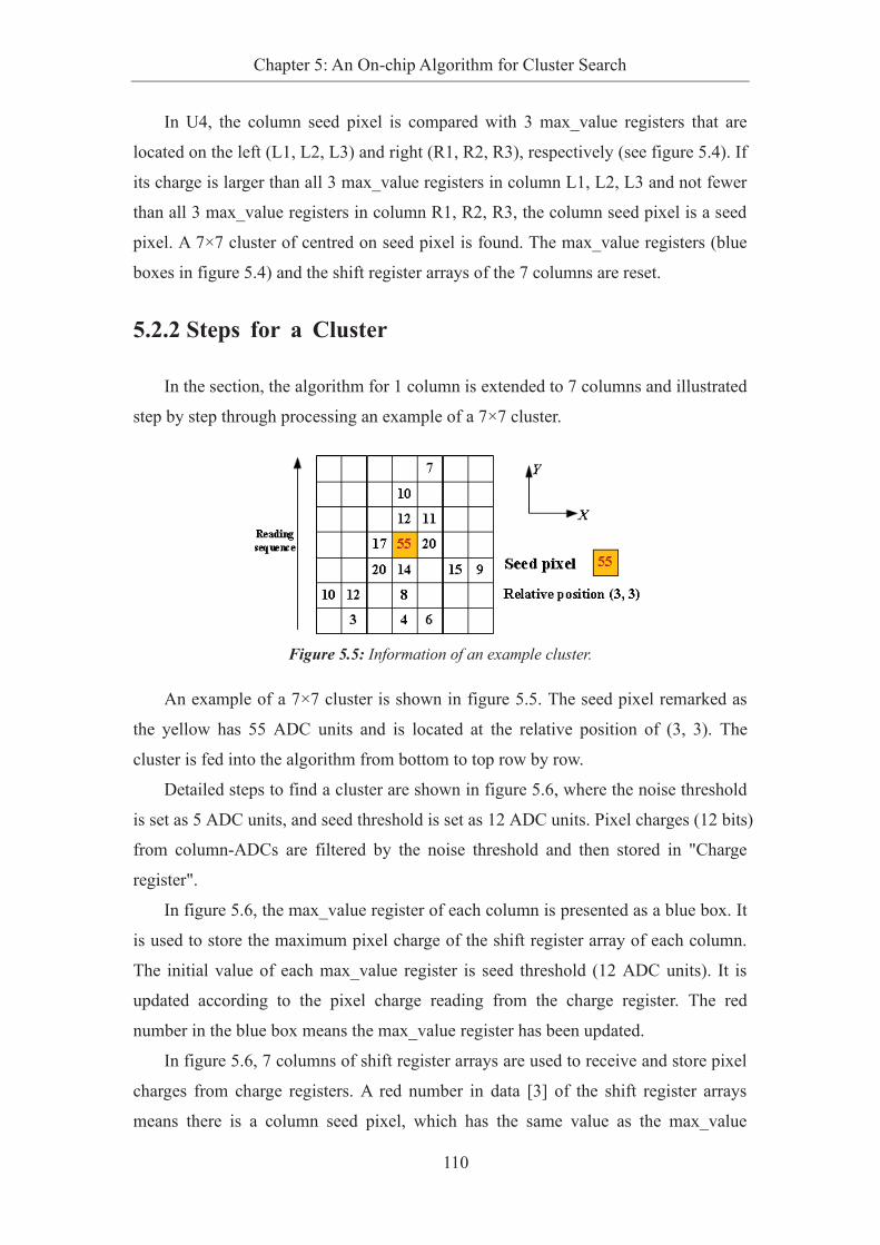
Chapter 5: An On-chip Algorithm for Cluster Search
110
In U4, the column seed pixel is compared with 3 max_value registers that are
located on the left (L1, L2, L3) and right (R1, R2, R3), respectively (see figure 5.4). If
its charge is larger than all 3 max_value registers in column L1, L2, L3 and not fewer
than all 3 max_value registers in column R1, R2, R3, the column seed pixel is a seed
pixel. A 7×7 cluster of centred on seed pixel is found. The max_value registers (blue
boxes in figure 5.4) and the shift register arrays of the 7 columns are reset.
5.2.2 Steps for a Cluster
In the section, the algorithm for 1 column is extended to 7 columns and illustrated
step by step through processing an example of a 7×7 cluster.
Figure 5.5: Information of an example cluster.
An example of a 7×7 cluster is shown in figure 5.5. The seed pixel remarked as
the yellow has 55 ADC units and is located at the relative position of (3, 3). The
cluster is fed into the algorithm from bottom to top row by row.
Detailed steps to find a cluster are shown in figure 5.6, where the noise threshold
is set as 5 ADC units, and seed threshold is set as 12 ADC units. Pixel charges (12 bits)
from column-ADCs are filtered by the noise threshold and then stored in "Charge
register".
In figure 5.6, the max_value register of each column is presented as a blue box. It
is used to store the maximum pixel charge of the shift register array of each column.
The initial value of each max_value register is seed threshold (12 ADC units). It is
updated according to the pixel charge reading from the charge register. The red
number in the blue box means the max_value register has been updated.
In figure 5.6, 7 columns of shift register arrays are used to receive and store pixel
charges from charge registers. A red number in data [3] of the shift register arrays
means there is a column seed pixel, which has the same value as the max_value
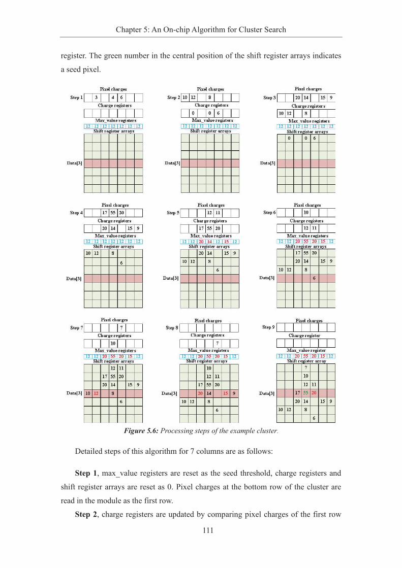
Chapter 5: An On-chip Algorithm for Cluster Search
111
register. The green number in the central position of the shift register arrays indicates
a seed pixel.
Figure 5.6: Processing steps of the example cluster.
Detailed steps of this algorithm for 7 columns are as follows:
Step 1, max_value registers are reset as the seed threshold, charge registers and
shift register arrays are reset as 0. Pixel charges at the bottom row of the cluster are
read in the module as the first row.
Step 2, charge registers are updated by comparing pixel charges of the first row

Chapter 5: An On-chip Algorithm for Cluster Search
112
with the noise threshold. Just one charge register is updated as 6 ADC units and other
pixel charges of the first row are fewer than the noise threshold.
Step 3, max_value registers and the first row of the shift register arrays are
updated according to charge registers. Max_value registers do not be updated since all
values are fewer than the initial value of max_value registers (12 ADC units). Then
charge registers are updated by pixel charges of the second row.
Step 4, values stored in shift register arrays are shifted from top to bottom and the
top row is filled by values of charge registers. Values of max_value registers are not
varied. Then charge registers are updated by pixel charges of the third row.
Step 5, max_value registers of column [2], column [3] and column [5] are
updated as 20 ADC units, 14 ADC units, 15 ADC units, respectively. In max_value
registers (see blue boxes in figure 5.6), the number marked in red indicates that it has
been updated.
Step 7, in shift register arrays, the pixel charge stored in data [3] of column [1] is
recognized as a column seed pixel and marked in red. The pixel charge is equal to the
max_value register. But it cannot be a seed pixel since it is not larger than 3
max_value registers of its left columns (L3, L2, L1).
Step 8, two column seed pixels are found in column [2] and column [5] and
marked as red in shift register arrays. For the column seed pixel in column [2], its
value (20 ADC units) is fewer than the max_value register (55 ADC units) of column
R1 (column [3]), so it cannot be a seed pixel. It is the same explanation that the
column seed pixel with 15 ADC units in column [5] is not a seed pixel.
Step 9, the pixel stored in data [3] of the column [3] marked in green indicates
that it is a seed pixel. It is a column seed pixel as it is equal to the max_value register,
and it is a seed pixel since it has the largest value compared with a total of 6
max_value registers of the left and right columns (L1-L3, R1-R3).
5.2.3 Supplementary Explanation
Two issues of the algorithm are explained in detail, charges of column seed pixels
and two "seed pixels" in one cluster.
1. Charges of column seed pixels
As shown in step 7 of figure 5.6, data [3] of column [1] (12 ADC units) is a
column seed pixel but it is not larger than the seed threshold (12 ADC units), and it is

Chapter 5: An On-chip Algorithm for Cluster Search
113
not a seed pixel. In order to explain the correlation between the column seed pixel
charge and the seed threshold clearly, three situations are presented and analysed.
Ø Column seed pixel charge < seed threshold (12 ADC units).
Impossible. A column seed pixel means that data [3] is equal to the
max_value register. The minimum value of the max_value register is the
seed threshold (12 ADC units).
Ø Column seed pixel charge = seed threshold (12 ADC units).
If the pixel charge stored in data [3] is 12 ADC and the max_value
register keeps the initial value (12 ADC units). The pixel stored in data [3]
is defined as a column seed pixel since it is equal to the max_value
register.
However, it cannot be a seed pixel. The column seed pixel is defined
as a seed pixel only if it is larger than all 3 max_value registers of left
columns and not fewer than all 3 max_value registers in right columns.
The minimum value of these six registers is 12 ADC units. The column
seed pixel cannot be a seed pixel.
As shown in step 7 of figure 5.6, the pixel stored in data [3] of
column [1] is recognized as a column seed pixel but not a seed pixel.
Ø Data [3] > 12 ADC units.
If the pixel charge stored in data [3] is equal to the max_value
register, it is defined as a column seed pixel.
Meanwhile, if it is larger than all 3 max_value registers of left
columns and not fewer than all 3 max_value registers of right columns, it
is a seed pixel.
2. Two "seed pixels"
A seed pixel has the largest pixel charge compared with other pixels around it in
the 7×7 cluster window. A pixel that has the same value as the seed pixel is allowed to
be located in the first quadrant of a coordinate axis which is centred on the seed pixel.
The case is shown and explained in two aspects according to the location of the pixel.

Chapter 5: An On-chip Algorithm for Cluster Search
114
Ø The pixel located above (a1, a2, a3) the seed pixel.
Figure 5.7: Two "seed pixels" in the same column, pixel A is the seed pixel, pixel B is a part of
the cluster.
As shown in figure 5.7, an example of a 7×7 cluster has a seed pixel
with 55 ADC unit. A pixel (pixel_B) located above the seed pixel has the
same pixel charge.
The cluster is read in row by row from the bottom to the top. The
pixel_A which is read in the algorithm firstly will be identified as a seed
pixel, and the pixel_B read later will be recognized as part of the cluster.
The seed pixel is determined according to the reading sequence if two or
more pixels have the same value with the seed pixel in the column.
Ø The pixel located on the right (R1, R2, R3) of the seed pixel.
Figure 5.8: Two "seed pixels" in the same row, pixel A is the seed pixel, pixel B is a part of the
cluster.
As shown in figure 5.8, an example of a 7×7 cluster has a seed pixel

Chapter 5: An On-chip Algorithm for Cluster Search
115
with 55 ADC units. A pixel (pixel_B) located in the right has the same
pixel charge.
According to the original definition of a seed pixel, it has to be larger
than all 6 max_value registers of the left and right columns (L1-L3,
R1-R3). There is no seed pixel in this 7×7 cluster window since the charge
of pixel_A is not larger than the max_value register of column [5] which
is also equal to 55 ADC units, the cluster would be lost by the definition.
It is same for the pixel_B.
In order to prevent missing some clusters, the definition of the seed
pixel is optimised and expressed in module U4 of the algorithm. A seed
pixel is larger than 3 max_value registers of left columns (L1, L2, L3) and
not fewer than 3 max_value registers in right columns (R1, R2, R3).
According to the definition in the algorithm, pixel_A in the column [3]
recognized as a seed pixel as it is not fewer than the pixel_B. Pixel_B in
the column [5] cannot be recognized as a seed pixel since it is not larger
than the pixel_A.
5.3 Simulation Results
In order to analyse the performance of the algorithm proposed in the chapter, the
algorithm was extended for a 256-column input and achieved by the C code.
As described in chapter 4, 500 frames of raw data for each given incident angle
(total 10 angles) were collected and preprocessed to test the ANN implemented in the
FPGA. Matrices of pixel charges are also used to test the algorithm proposed in the
chapter. Each frame of pixel charges is 256×256 pixels.
In the section, algorithms with different cluster windows, seed thresholds are
simulated, and they are compared with the algorithm implemented in the FPGA device.
The cluster count means the number of clusters found in 500 frames of pixel charges for
a given incident angle
5.3.1 Cluster Windows
A cluster window is used to limit the maximum area of a cluster. It is necessary

Chapter 5: An On-chip Algorithm for Cluster Search
116
for the algorithm proposed to define a seed pixel and collect cluster information. A
seed pixel has the largest pixel charge in a cluster window instead of the whole
256×256 pixels matrix.
By the algorithm proposed, the range of incident angles that can be detected is
proportional with the size of a cluster window. As shown in figure 4.11 and formula
(4-21), the maximum incident angle that can be detected is 78.6 degrees by the 7×7
cluster window. The sharp increase at incident angle θinc = 50 degrees has been
explained in figure 4.16.
Figure 5.9: Simulation results of cluster counts found by algorithms proposed in this chapter
with different cluster windows (7×7 and 5×5 cluster window).
Cluster counts found by algorithms with different cluster windows are shown in
figure 5.9. It can be observed that cluster counts defined by different cluster windows
(5×5 and 7×7 cluster window) [3][4] have the same variety trend. Cluster counts
found by the two algorithms decrease as the incident angle θinc increases.
Cluster counts found by different cluster windows do not differ significantly for
the incident angle θinc less than 55 degrees. As the incident angle θinc increases, more
and more clusters owning elongated shapes appear. Some of the clusters between 5×5
pixels and 7×7 pixels are recognized by the 5×5 cluster window as two or more
clusters. As shown in figure 5.9, the gap between the cluster counts of the two
algorithms is expanded for a large incident angle.
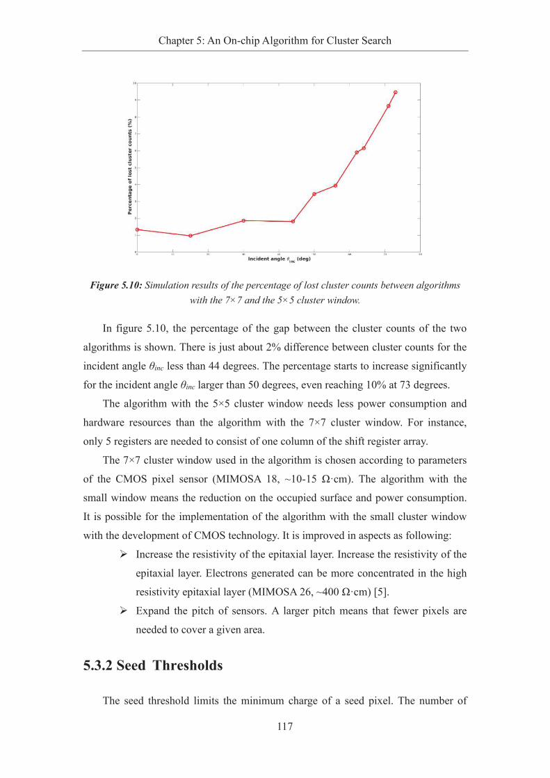
Chapter 5: An On-chip Algorithm for Cluster Search
117
Figure 5.10: Simulation results of the percentage of lost cluster counts between algorithms
with the 7×7 and the 5×5 cluster window.
In figure 5.10, the percentage of the gap between the cluster counts of the two
algorithms is shown. There is just about 2% difference between cluster counts for the
incident angle θinc less than 44 degrees. The percentage starts to increase significantly
for the incident angle θinc larger than 50 degrees, even reaching 10% at 73 degrees.
The algorithm with the 5×5 cluster window needs less power consumption and
hardware resources than the algorithm with the 7×7 cluster window. For instance,
only 5 registers are needed to consist of one column of the shift register array.
The 7×7 cluster window used in the algorithm is chosen according to parameters
of the CMOS pixel sensor (MIMOSA 18, ~10-15 Ω·cm). The algorithm with the
small window means the reduction on the occupied surface and power consumption.
It is possible for the implementation of the algorithm with the small cluster window
with the development of CMOS technology. It is improved in aspects as following:
Ø Increase the resistivity of the epitaxial layer. Increase the resistivity of the
epitaxial layer. Electrons generated can be more concentrated in the high
resistivity epitaxial layer (MIMOSA 26, ~400 Ω·cm) [5].
Ø Expand the pitch of sensors. A larger pitch means that fewer pixels are
needed to cover a given area.
5.3.2 Seed Thresholds
The seed threshold limits the minimum charge of a seed pixel. The number of

Chapter 5: An On-chip Algorithm for Cluster Search
118
clusters is directly affected by the seed threshold. Seed thresholds of the algorithm are
set at different levels to simulate.
Figure 5.11: Simulation results of cluster counts by algorithms with different seed thresholds.
In figure 5.11, cluster counts found by algorithms with different seed thresholds
(2.4×noise threshold, 3×noise threshold, 4×noise threshold and 5×noise threshold) are
presented, respectively. As the reference result, cluster counts found by the algorithm
implemented in the FPGA (seed threshold = 2.4×noise threshold) is shown. Cluster
counts by different seed thresholds have the same decrease trend with increasing the
incident angle. It can be observed that, as the seed threshold increases, cluster counts
decrease. Cluster counts have the most obvious decrease when the seed threshold
increase from 2.4×noise threshold units to 3×noise threshold units.
5.3.3 Algorithm in the FPGA VS. Algorithm Proposed
The algorithm for cluster search implemented in the FPGA device has been
validated by the design implemented in the TMVA. Main steps of the algorithm with
the 7×7 cluster window are as follows:
1. Scanning pixel charges of a 256×256 matrix, finding out a seed pixel which
has the maximum charge, and storing in a register array;
2. Erasing the seed pixel charge from the matrix;
3. Checking 8 neighbour pixels around the seed pixel in a 3×3 cluster window.
Find fired pixels from the 8 neighbour pixels, store their relative positions and

Chapter 5: An On-chip Algorithm for Cluster Search
119
pixel charges in a register array;
4. Erasing these fired pixel charges from the matrix;
5. Repeating step 3-4 around pixels stored in the register array until there is no
new pixel or the search area exceeds the 7×7 cluster window2;
6. Outputting this cluster information and reset the register array;
7. Finding the next seed pixel in the 256×256 matrix, or read in the next matrix
of pixel charges if there is no seed pixel.
As shown in figure 5.12, cluster counts by the algorithm proposed and the
algorithm implemented in the FPGA device (with 7×7 cluster window and without
cluster window) for each given incident angle are simulated. The algorithm without
the cluster window means no limitation on the cluster size, the cluster is defined just
by the connectivity between fired pixels and the seed pixel.
Figure 5.12: Simulation results of cluster counts found by the algorithm proposed VS.
implemented in the FPGA device.
Cluster counts by these algorithms have the same trend. Due to the influence of
the size change of the effective detection surface, cluster counts decrease as the
incident angle increases.
There is no significant difference among cluster counts obtained by the three
2 . For the algorithm without the cluster window, this step will stop only when there is no new
pixel stored in the register array.

Chapter 5: An On-chip Algorithm for Cluster Search
120
algorithms for the incident angle less than 55 degrees. As the incident angle θinc
increases, especially larger than 55 degrees, cluster counts have a significant
difference between the two algorithms implemented in the FPGA device. The number
of clusters owning elongated shape increases with the growth of incident angle θinc.
An elongated cluster defined by the algorithm without the cluster window will be
recognized as two or more clusters by an algorithm with a 7×7 cluster window.
As shown in figure 5.12, the algorithm proposed reaches the same level of cluster
counts as the other two algorithms. The algorithm proposed limits the cluster in a 7×7
area, leading to that its cluster counts are larger than those found by the algorithm
without the cluster window. The algorithm proposed has no modules to check
neighbour pixels of a seed pixel, leading to missing separated clusters located in one
cluster window. These issues are discussed detailly in the next section.
5.4 Discussion
In order to make a deep understanding of the algorithm proposed and explain the
difference between the algorithm proposed and the algorithm implemented in the
FPGA further, these algorithms are discussed for three examples of special cluster cases,
including large clusters, separated parts located in a cluster window and overlap parts of
two clusters.
5.4.1 Large Clusters
Compared with the algorithm with the 7×7 cluster window implemented in the
FPGA device, the algorithm proposed can reduce the possibility that one large cluster
is recognized as two or more clusters.
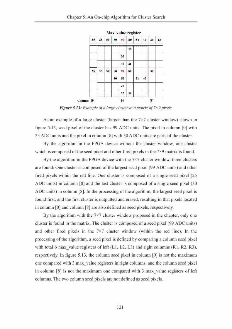
Chapter 5: An On-chip Algorithm for Cluster Search
121
Figure 5.13: Example of a large cluster in a matrix of 7×9 pixels.
As an example of a large cluster (larger than the 7×7 cluster window) shown in
figure 5.13, seed pixel of the cluster has 99 ADC units. The pixel in column [0] with
25 ADC units and the pixel in column [8] with 30 ADC units are parts of the cluster.
By the algorithm in the FPGA device without the cluster window, one cluster
which is composed of the seed pixel and other fired pixels in the 7×9 matrix is found.
By the algorithm in the FPGA device with the 7×7 cluster window, three clusters
are found. One cluster is composed of the largest seed pixel (99 ADC units) and other
fired pixels within the red line. One cluster is composed of a single seed pixel (25
ADC units) in column [0] and the last cluster is composed of a single seed pixel (30
ADC units) in column [8]. In the processing of the algorithm, the largest seed pixel is
found first, and the first cluster is outputted and erased, resulting in that pixels located
in column [0] and column [8] are also defined as seed pixels, respectively.
By the algorithm with the 7×7 cluster window proposed in the chapter, only one
cluster is found in the matrix. The cluster is composed of a seed pixel (99 ADC units)
and other fired pixels in the 7×7 cluster window (within the red line). In the
processing of the algorithm, a seed pixel is defined by comparing a column seed pixel
with total 6 max_value registers of left (L1, L2, L3) and right columns (R1, R2, R3),
respectively. In figure 5.13, the column seed pixel in column [0] is not the maximum
one compared with 3 max_value registers in right columns, and the column seed pixel
in column [8] is not the maximum one compared with 3 max_value registers of left
columns. The two column seed pixels are not defined as seed pixels.

Chapter 5: An On-chip Algorithm for Cluster Search
122
5.4.2 Separated Parts
Due to no extra design to check connectivity among pixels, the algorithm
proposed recognizes separated parts located in one cluster window as one cluster,
leading to the reduction on cluster counts.
Figure 5.14: Example of separated parts in a matrix of 7×7 pixels.
An example of separated parts located in a 7×7 cluster window is shown in figure
5.14. In general, the example will be recognized as two clusters. One cluster
composed of three pixels on the left top corner of this matrix. The other cluster is
composed of a seed pixel (55 ADC units) and other fired pixels.
The two clusters will be found by two algorithms (without the cluster window
and with a 7×7 cluster window) implemented in the FPGA device. The connectivity
between fired pixels and the seed pixel as one of the conditions is taken into account
to define a cluster.
By the algorithm proposed, only one cluster is found. The cluster contains a seed
pixel (55 ADC units) and other all fired pixels in the matrix (including 3 pixels on the
left top corner). Considering hardware resources and operation time of the algorithm,
the design for detecting connectivity is dropped.
In fact, it is uncertain about the attribution of these three pixels located on the left
top corner. They are recognized as an individual cluster since they are separated from
the seed pixel. On the other hand, they are recognized as a part of the cluster if one or
some blue pixels in the matrix have charges exceeding the noise threshold.

Chapter 5: An On-chip Algorithm for Cluster Search
123
5.4.3 Overlap Parts
Due to the limitation of resources and the complexity of conditions, both the
algorithm proposed and the algorithm implemented in the FPGA have no effective
reaction on the parts overlapped by two cluster.
Figure 5.15: Example of overlap parts in a matrix of 8×7 pixels.
An example of the overlap part of two clusters is shown in figure 5.15. There are
two seed pixels (55 ADC units and 44 ADC units) in the matrix of 8×7 pixels.
By the algorithm in the FPGA device without the cluster window, one cluster is
found in the 8×7 matrix. The cluster is composed of a seed pixel (55 ADC units) and
the other fired pixels, including the pixel marked with red (44 ADC units).
By the algorithm in the FPGA device with the 7×7 cluster window, two clusters
are found. One cluster is composed of a seed pixel (55 ADC units) and other fired
pixels. The other cluster is composed of a single pixel with 44 ADC units.
Two clusters are found by the algorithm proposed in the chapter. One cluster is
composed of a seed pixel (55 ADC units) and the other fired pixels in the matrix
(within the red line). The other cluster is a single seed pixel marked by red (44 ADC
units). All pixels located between two seed pixels belong to the first cluster. In the
algorithm proposed, only 7 rows of pixel charges are stored in the shift register array,
the pixel located out of the size cannot be taken into account. In addition, the search
result is related to the reading sequence, it makes totally different results if pixel
charges are read from top to bottom of the matrix.
For the 7×7 cluster window, charges of these pixels located between these two

Chapter 5: An On-chip Algorithm for Cluster Search
124
seed pixels should be allocated into two clusters based on values of the two seed
pixels. However, it means additional hardware resources and power consumption to
store more pixel charges and allocate overlap parts into two or more clusters.
Considering the balance between the possibility and hardware resources, this situation
would not be taken into account.
5.5 Algorithm Implementation
In the section, firstly, the implementation of the 64-column algorithm achieved by
Hardware Description Language (HDL) is described. Next, Operation timing of the
signals and data is illustrated. Then, the implementation of a 256-column algorithm
achieved by C language is described and tested. Finally, the power consumption and
occupied surface of the 64-column implementation are synthesized targeted at the
TowerJazz 0.18 µm process.
5.5.1 Implementation of the 64-column Algorithm
The implementation of the algorithm proposed is based on modules of the
2N-column matrix. An example structure of two 32-column (N=5) modules
implemented for a 64-column input is shown in figure 5.16. Pixel charges are read in
from 64 column-level ADCs row by row and then fed to the two 32-column modules.
Each 32-column module has two levels (level 1 and level 2).

Chapter 5: An On-chip Algorithm for Cluster Search
125
Figure 5.16: Schematic of the algorithm implemented in 64 columns.
Implementation of level 1
Level 1 consists of 32 cluster search units, each of which is the implementation of

Chapter 5: An On-chip Algorithm for Cluster Search
126
the algorithm for cluster search proposed in the chapter. The pixel charge from a
column-level ADC is fed into the unit and a signal named "seed_pixel_en" is outputted.
A high-level pulse of one clock cycle will be generated on its signal "seed_pixel_en" if
a seed pixel is found in the column.
Figure 5.17: Implementation of the cluster search unit.
The implementation circuit of the cluster search unit is shown in figure 5.17. The
input of the unit is the pixel charge. The noise threshold and the seed threshold are fixed
in registers. The output of the unit is the signal “seed_pixel_en”.
The pixel charge is filtered by the noise threshold in U0, then inputted to U1 and
U2. U2 is a register array that is used to store 7 consecutive pixel charges of a column.
U1 is used to record the maximum pixel charge stored in U2.
In U3, the maximum pixel charge stored in U1 is compared with data [3] of U2. A
column seed pixel is found if the maximum pixel charge is equal to data [3], then a
pulse of one clock cycle will be generated on the signal "column_seed_pixel".
In U4_0, 3 max_value registers (“right_1_neighbour_value”,
“right_2_neighbour_value” and “right_3_neighbour_value”) of right columns are
inputted and compared with the max_value register of this column. 3 comparison
results are outputted to U4_1. 3 comparison results (“left_1_neighbour_result”,
“left_2_neighbour_result” and “left_3_neighbour_result”) between 3 max_value
registers of left columns and the max_value register of this column are inputted. “AND”
operation is applied among the six comparison results in module U4_1. The result of
“AND” operation is equal to 1 if the max_value register of this column is larger than 3
max_value registers of the left columns and not fewer than 3 max_value registers of

Chapter 5: An On-chip Algorithm for Cluster Search
127
right columns. Then a pulse of one clock cycle would be generated on the signal
“row_max”.
If a pulse signal is simultaneously generated on the signal "row_max" and the
signal "column_seed_pixel", a pulse of one clock cycle will be created on the signal
“seed_pixel_en”, which means that the seed pixel is found.
Implementation of level 2
In theory, one module to collect 7×7 cluster information is required for each
column, which means a total of 32 modules are needed following level 1. In order to
reduce power consumption and the occupied surface, and considering the hit density in
a matrix [6], an extra multiplexer array is implemented between the level 1 and
collection modules resulting in that just one module for cluster collection is needed for
32 columns. As shown in figure 5.16, level 2 is a multiplexer array which is composed
of seven (for the 7×7 cluster window) units of the 32-1 multiplexer. The 32-1
multiplexer at middle position is used to detect the seed pixel and collect pixel charges
of the middle column of a cluster, and other 6 multiplexers are used to choose and
collect pixel charges of left and right columns of the seed pixel (L1-L3, R1-R3).
In level 2, 3 additional data buses are connected with the ground at the left side.
They are used to supply pixel charges of 3 left columns if signal “seed_pixel_en” of
column [0] is active. It is the same for other 3 additional data buses on the right side of
the right multiplexer array.
In level 2, 3 data buses at the right side are connected with data_bus_32,
data_bus_33, and data_bus_34. They are used to supply pixel charges of 3 right
columns if signal “seed_pixel_en” of column [31] is active. It is the same reason for
connections between data_bus_29, data_bus_30, data_bus_31 and the right multiplexer
array.
The case that a boundary pixel is also taken into account in the design of level 1.
These designs guarantee to collect complete pixel charges of a cluster if a seed pixel is
located at the boundary column of the pixel charge matrix.
5.5.2 Timing
In level 2, signals “seed_pixel_en” of 32 columns are received and scanned from
left to right. In the case that pulses are detected on more than one signal “seed_pixel_en”

Chapter 5: An On-chip Algorithm for Cluster Search
128
at the same time, the pulse of the column which is scanned firstly is chosen as a seed
pixel, and the other pulses are abandoned.
In figure 5.18 shows an example of related signal waveforms when two seed pixels
are found in the same row of 32 columns. "Column 4 input" and "Column 18 input" are
pixel charges coming from column-level ADCs. Red numbers in these signals mean
that there are two seed pixels in the two columns, one seed pixel charge is 40 ADC units
and the other is 50 ADC units. Pulses on signals "Column 4 seed_pixel_en" and
"Column 18 seed_pixel_en" mean that two seed pixels are found by level 1 at the same
time. There are 4 clock cycles from pulses on signal "Column 4 input" to pulses on
signal "Column 4 seed_pixel_en". The delay is used to search for seed pixels and
generate pulses. Signals "Column output" is the output of a cluster search unit. The seed
pixel in column [4] is chosen as a seed pixel. The seed pixel in column [18] is
abandoned since the pulse on signal “seed_pixel_en” of column [4] is scanned firstly. A
high-level pulse of 7 clock cycle is generated on signal “MUX_en” to read out cluster
information when a pulse on the signal “seed_pixel_en” is detected.
Figure 5.18: Timing of generating two seed pixels at one row.
New pulses will be abandoned if they are generated within the 7 clock cycles active
time of signal “MUX_en”. It means that new seed pixels cannot be collected if they are
located within 6 rows away from the seed pixel which is outputted last time. The
implementation of the multiplexer array affects the cluster count. It is simulated in the
next section.

Chapter 5: An On-chip Algorithm for Cluster Search
129
5.5.3 Simulation of the 256-column Implementation
Implementation of the 64-column algorithm with the multiplexer array is extended
to 256 columns and achieved by C code. 500 frames of pixel charges for each given
angle are fed into to simulate the design. In addition to modules of the 32-column
matrix shown in figure 5.16, modules of the 16-column matrix and the 64-column
matrix are also implemented for comparison. Cluster counts found by different modules
are shown in figure 5.19. The implementation proposed without multiplexer refers to an
ideal situation.
Figure 5.19: Simulation of cluster counts found by the algorithm with different modules.
Due to the influence of the read-out sequence and the reset control, there is a
difference in simulation results between implementations with multiplexers and
without multiplexer (the ideal situation). As shown in figure 5.19, for the incident angle
larger than 50 degrees, the difference is extended as the more elongated clusters are
generated in the matrix. By the design without multiplexer, an elongated cluster will be
divided into two or more clusters that all are collected, by the design with multiplexers,
just one seed pixel is allowed in one row of 32 columns (or 64 columns).
Cluster counts simulated decrease as the column number of inputs of a multiplexer
module increases. As shown in figure 5.19, the cluster counts simulated with the
module of the 64-column matrix is the least in simulation results. In fact, the
implementation with modules of the 32-column matrix and the 7×7 cluster window

Chapter 5: An On-chip Algorithm for Cluster Search
130
means that only one cluster can be collected in a pixel matrix of 10 rows by 32 columns.
The implementation with modules of the 64-column matrix can collect one cluster in a
pixel matrix of 10 rows by 64 columns.
5.5.4 Synthesized Result of the 64-column Implementation
The occupied surface and power consumption of the 64-column implementation
(shown in figure 5.16) are synthesized using Cadence EDA tools targeted at the
TowerJazz 0.18 µm process, as shown in Table 5-1. The column height (occupied
surface) and the column power (power consumption) are average values. The column
pitch is set to 50 µm.
Table 5-1: Simulation results of the occupied surface and power consumption of the 64-column
implementation.
Window Multiplexer
ADC
bits
Clock
(MHz)
Column
height
(µm)
Column
power
(mW)
7×7 16-1
8 100 200.58 0.85
8 200 200.15 1.83
4 100 102.86 0.46
4 200 103.39 0.88
7×7 32-1
8 100 197.81 0.86
8 200 197.24 1.77
4 100 101.08 0.43
4 200 102.24 0.88
5×5 32-1
8 100 159.39 0.68
8 200 159.2 1.45
4 100 81.56 0.37
4 200 82.92 0.71
7×7 64-1
8 100 196.83 0.87
8 200 196.09 1.76
4 100 101.26 0.43
4 200 101.63 0.9
As shown in Table 5-1. The occupied surface and power consumption can be

Chapter 5: An On-chip Algorithm for Cluster Search
131
reduced if the 5×5 window is used instead of the 7×7 window. The trade-off between
power consumption and search efficiency of the two designs, in addition, the
comprehensiveness and accuracy of cluster information that is supplied to the MCA
module, are considered in our design.
Both the occupied surface and power consumption can be reduced obviously if a
low-frequency clock or a low-resolution ADC is employed. Almost the occupied
surface and power consumption are reduced to about 50% if the ADC resolution is
changed from 8 bits to 4 bits. Power consumption can be reduced to half if a 100 MHz
system clock is taken instead of 200MHz, but no obvious difference is observed in
term of the occupied surface.
In detail, the most power consumption of this design is devoted by shift register
arrays, almost 50% in the design with the 7×7 cluster window. A shift register array
needs to operate 7 times of data shifting per clock cycle. The design with the 5×5
cluster window contributes less power consumption than that with the 7×7 cluster
window since fewer shift registers are needed store pixel charges.
There is no significant difference on the occupied surface (column height) and
power consumption (column power) among implementations with modules of the
16-column matrix, the 32-column matrix and the 64-column matrix.
Figure 5.20: Schematic of MCA and ANN modules implemented for modules of the 32-column
matrix.
However, considering the feature extraction (MCA) module and ANN module
following the design of cluster search, more occupied surface and power consumption
are needed if modules of the 16-column matrix are used in the implementation. As
shown in figure 5.20, for a 64-column implementation, two feature extraction
modules and two ANN modules are used for the design with modules of the

Chapter 5: An On-chip Algorithm for Cluster Search
132
32-column matrix. Only one feature extraction module and one ANN module are
needed if modules of the 64-column matrix are used in the implementation. Four
times the occupied surface and power consumption are needed for the feature
extraction module and the ANN module if modules of the 16-column matrix are used.
5.6 Summary
The algorithm for cluster search implemented in the FPGA device is impossible
to transplant to the ASIC design since a lot of memory resource and operation time
are needed. An on-chip algorithm for cluster search is introduced which can find seed
pixels and locate clusters in a cluster window in real-time. The algorithm with
different cluster windows and different seed thresholds are achieved by C code and
simulated. Cluster counts found by the algorithm is compared with those found by the
algorithm implemented in the FPGA device and reach the same level of cluster counts
as the algorithm in the FPGA.
The algorithm can be integrated into the CMOS pixel sensor and executed in
real-time. In the implementation of the algorithm, the multiplexer array is employed
following the module of cluster search to reduce the power consumption and occupied
surface of the MCA and ANN modules.
In the term of implementation, power consumption can be reduced by optimizing
the control system. The power gating technology can be used to shut off the current of
modules that are not used. The modules will be activated only when a seed pixel is
found, a majority part of power consumption would be reduced since there are a few
seed pixels in one frame.
Chapter 5: An On-chip Algorithm for Cluster Search
133
5.7 Bibliography
[1]. Johnston, Christopher T., and Donald G. Bailey. "FPGA implementation of a single pass
connected components algorithm." 4th IEEE International Symposium on Electronic
Design, Test and Applications (delta 2008). IEEE, 2008.
[2]. Rosenfeld, Azriel, and John L. Pfaltz. "Sequential operations in digital picture
processing." Journal of the ACM (JACM) 13.4 (1966): 471-494.
[3]. Kohrs, R., et al. "First test beam results on DEPFET pixels for the ILC." Nuclear
Instruments and Methods in Physics Research Section A: Accelerators, Spectrometers,
Detectors and Associated Equipment 565.1 (2006): 172-177.
[4]. Miho Yamada, “Development of Vertex Detector for ILC”, SOI Satellite Meeting,
Strasbourg, France May. 9th, 2017.
[5]. Hu-Guo, Christine, I. P. H. C. Collaboration, and I. R. F. U. Collaboration. "Development
of fast and high precision CMOS pixel sensors for an ILC vertex detector." arXiv preprint
arXiv:1007.2634 (2010).
[6]. Strom, D. "Aspects of the sid detector design for the international linear
collider." Astroparticle, Particle And Space Physics, Detectors And Medical Physics
Applications. 2008. 511-520.


135
6 Conclusions and Perspectives
Conclusions
The International Linear Collider (ILC) is an e+/e- linear colliding experiment
project that will allow studying extensively the Higgs Boson properties. It is foreseen to
start commissioning phase about 2030. In order to meet high precision tagging
requirements, especially for short lived particles, excellent vertexing system will be
developed. One of the two detectors, the International Large Detector (ILD) will be
equipped in the ILC. The vertex detector is located at the most inner layer to measure
the primary interaction vertex and secondary vertices from decay particles under
cooperation from other tracking detectors. For the last decade, CMOS pixel sensors,
also named Monolithic Active Pixel Sensors (MAPS), proposed and extensively
researched by the PICSEL group in IPHC, have been employed for charged particle
tracking and imaging.
In the vertex detector of the ILC, a large amount of extra hits will be generated by
electrons coming from the beam background. Momenta of these background electrons
typically lie in the range of 10-100 MeV/c, which is lower than particles coming from
physics events. Due to the effect of multiple scattering, in the multi-layer structure of
vertex detectors in the ILD, challenges are obviously presented for track reconstruction
of low momentum particles.
The thesis focused on the development of a CMOS pixel sensor with on-chip
Artificial Neural Networks (ANNs) to tag and remove hits generated by background
particles (typical low momenta). The existence of the magnetic field in the detector

Chapter 6: Conclusions and Perspectives
136
leads to particles make helix paths. In addition, low momenta of particles lead to large
incident angles with respect to the normal of the sensor planes. Considering the MAPS
equipped in the vertex detector, when a charged particle traverses the epitaxial layer of
the MAPS, electron-hole pairs are created by the ionization process (typical ~80
e-h/µm). Electrons are collected by the collection diode of each pixel. Because of
diffusion, electrons will be collected by several independent pixels. These independent
pixels constitute a charge cluster which expresses hit information. Particles from beam
background (typical low momenta) hit on the vertex detector, resulting in the
generation of rather elongated cluster shapes.
Artificial Neural Networks (ANNs) are computational modules that are inspired by
biological neural networks. Our group proposed to integrate ANNs into the CMOS
pixel sensor for reconstructing the incident angle based on each cluster.
1. The implementation in a FPGA device.
For the feasibility study, preprocessing modules and the ANN structure have been
implemented in a FPGA development board and validated by the ANN implemented in
the TMVA. Both implementations are operated in an offline method, which means that
procedures of data acquisition and process are separated.
A raw data acquisition system is established to collect raw data from an existing
sensor MIMOSA 18, which is exposed under the illumination of β⁻ source 90Sr. Incident
angles of raw data can be varied by adjusting the angle between the system and the
reference plane. Raw data was collected for each given incident angle (total 10 incident
angles) to train weights of the ANN by the TMVA.
I implemented preprocessing modules and the ANN in a NEXYS VIDEO FPGA
development board by Hardware Description Language (HDL). Raw data collected is
fed into the FPGA device from PC frame by frame. In the FPGA, raw data per pixel
(32-bit) is processed by the Correlated Double Sampling (CDS) to generate a 12-bit
pixel charge. Preprocessing modules mainly contain cluster search and feature
extraction. The cluster search module is used to find out seed pixels and locate clusters
(7×7 pixels) in a frame of pixel charges based on each seed pixel. Feature extraction
modules are used to produce features to represent a cluster.
The ANN module implemented in the FPGA device is a Multi-Layer Perceptron
(MLP) structure. The input layer is composed of four input neurons for taking the
cluster features into the network and one bias neuron. The four characteristics that were

Chapter 6: Conclusions and Perspectives
137
selected are the total charge of a cluster and the charge of the seed pixel, the maximum
and minimum standard deviations of charge distribution projected on an axis. These
four features are processed by normalization then fed into the ANN to reconstruct the
incident angle based on weights of the ANN. The hidden layer following the input layer
has 14 calculation neurons and 1 bias neuron. The activation function used in the ANN
is hyperbolic tangent.
In order to test the design implemented in the FPGA device, I have sampled 500
frames of raw data for each given incident angle. The raw data was fed into both the
ANN in the TMVA and implementation in the FPGA device. Reconstructed angles are
recorded and analysed.
Firstly, the feasibility study of transplanting the ANN design into hardware has
been validated. Mean values of angles reconstructed by TMVA and FPGA basically are
at the same level and show the same trend of the real incident angle. In addition, the
distribution of angles reconstructed by the FPGA device (θrec) shows that as the incident
angle of raw data increases, the proportion of large angles in the reconstruction results
increase, while the proportion of small angles decreases. Reconstructed results present
obvious same trend as the variety of incident angles and proof of the principle that tag
particles according to the incident angle based on the ANN has been established.
Meanwhile, mean values reconstructed by TMVA and FPGA are not completely
coincident, because of the difference in the data precision for hardware and software.
For example, in the Main Analysis Component (MCA) module which is used for
calculation of the maximum and minimum standard deviation, the lookup table design
is employed to provide values of the trigonometric function. Taking into account the
power consumption and processing time, the lookup table is at a step of 10 degrees,
while precision trigonometric values are supplied in the software.
According to the distribution of reconstructed angle, designs both in the FPGA and
the TMVA have not yet reached a precise level to predict the real incident angle, the
ANN structure and the training procedure still need to be optimized.
2. An on-chip algorithm for cluster search.
The module for cluster search implemented in the FPGA device cannot be
transplanted into the ASIC design directly. Firstly, a large number of memory resources
are needed to store the entire one frame of pixel charges; secondly, lots of resources and
time are needed to detect neighbour pixels. I propose an algorithm for cluster search. It

Chapter 6: Conclusions and Perspectives
138
can be integrated into the CMOS pixel sensor and collect clusters in real-time.
Instead of searching seed pixels in a matrix pixel by pixel, the algorithm seeks a
seed pixel in real-time in the read-in process of pixel charges row by row. The seed
pixel is admitted by comparing with pixels located above and below it and with largest
pixels located in the left and right columns of a certain window range.
I achieved the algorithm for 256-column by C code and simulated it. 500 frames of
raw data for each given incident angle are used to test the algorithm. The simulation
result shows that the algorithm reaches the same counting level as other algorithms
including the algorithm implemented in the FPGA device.
A unit of cluster search algorithm was designed according to the algorithm
described, which was implemented in each column of input. Consider the power
consumption and occupied surface of feature extraction and ANN modules following
cluster search modules, the implementation of the algorithm for multi-columns was
optimized. I achieved the implementation based on the modulo of 2N-column matrix,
which means channels of feature extraction and ANN module are input-column/2N.
I implemented the optimized design in a 64-column input and synthesis these
implementations targeted at the TowerJazz 0.18 µm CMOS process. There is no
significant difference among implementations with the modulo of 16-column (N=4),
32-column (N=5) and 64-column (N=6) in term of the occupied surface and power
consumption. However, considering the feature extraction and ANN module following
the implementation of cluster search, more occupied surface and power consumption
are needed if the modulo of 16-column is used. The occupied surface and power
consumption can be reduced if the 5×5 window is used instead of the 7×7 window. Both
the occupied surface and power consumption could be reduced obviously if a
low-frequency clock or a low-resolution ADC is employed.
The algorithm proposed can be integrated into the CMOS pixel sensor and
executed on pixel charges row by row in real-time. Simulation results show that the
algorithm achieves the consistent level on cluster counts with the algorithm for cluster
search implemented in the FPGA. Meanwhile, the algorithm makes improvement on
processing speed and reduction on the resource occupied. However, optimization and
improvement on power consumption and the occupied surface of the implementation
can be enhanced.
Perspectives

Chapter 6: Conclusions and Perspectives
139
On the basis of the research of the thesis, the concept of a CMOS pixel sensor with
on-chip artificial neural networks will be further studied from the following two
aspects:
1. Optimize the ANN to improve reconstruction precision.
The concept of CMOS pixel sensor with on-chip artificial neural networks is
validated by the ANN implemented in the FPGA device. However, neither of the two
reconstruction results can reach the exact prediction level, compared with real incident
angles.
More raw data will be acquired to retrained weights of the MLP structure used in
the thesis in order to improve the reconstruction precision.
The ANN architecture can be optimized. For example, taking into account the
trade-off between performance and resource of the design, more input neurons can be
introduced to present features of a cluster as complete as possible. Correspondingly, the
number of hidden neurons will also be adjusted accordingly. Even variety activation
functions and hidden layers can be employed and analysed.
New High-Level Synthesis (HLS) tools will be employed for the implementation
of the neural network. For example, the neural network structure is trained by
TensorFlow in Python, the hardware implementation of the neural network is
synthesized and optimized by Cadence Stratus HLS based on the module in Python.
The tool increases the efficiency and reduces the complexity of the hardware
implementation of a neural network.
2. Develop on-chip functional modules to realize the entire hardware design.
With respect to the implementation, some improvements can be carried out based
on the fabrication process targeted in the thesis (0.18 µm).
On the aspect of design. For the design of cluster search, the timing control can be
optimized to increase efficiency. For example, the application of power gating
technology can be used to reduce power consumption. For the module of feature
extraction, the implementation of the FPGA device is achieved by some intellectual
property mathematical function module, especially for the calculation of maximum and
minimum standard deviation. In order to reduce power consumption and improve the
operation speed, on-chip algorithms for feature extraction will be studied and
developed to integrate into the CMOS pixel sensor.
On the aspect of the material. The module of cluster search which is described in

Chapter 6: Conclusions and Perspectives
140
chapter 5 is the first level preprocessing modules followed the column-ADC. Due to
low resistivity of the epitaxial layer in the CPS (MIMOSA 18) which is used for raw
data acquisition, large shapes of clusters are produced, and the 7×7 cluster window is
employed. In CMOS pixel sensors equipped with the high resistivity epitaxial layer,
cluster shapes generated by charged particles will be lessened to 5×5 even 3×3 cluster
window, resulting in reduction on power consumption and occupied surfaces.
With the application of advanced fabrication processes (65 nm even 28 nm),
contributions will be made on the optimization and improvement of the hardware
implementation of the entire design.
A higher circuit density will be provided by the 65 nm fabrication process. The
cluster search module and feature extraction module can be achieved in distributed
units as integrated into pixels. The occupied surface of readout electronics will be
optimized, and the processing speed will be improved. On the aspect of power
consumption, the low power supply supported by the 65 nm fabrication process makes
a reduction on power consumption of the design.
Cluster search implementation
Seed pixels are located by comparing pixels row by row by the algorithm described
in chapter 5. However, by the advanced fabrication processes, comparators can be
integrated into pixels to tag fired pixels and compare signals from neighbour pixels. All
seed pixels and clusters in the pixel array will be extracted at the same time instead of
row by row. Combining with the low hit density of charged particles on the pixel array,
just comparators from a few pixels (fired pixels) are excited for cluster search, leading
to reduction of power consumption.
With the application of high resistivity material of the epitaxial layer, windows for
cluster search reduce to 5×5 pixels. A seed pixel can be located as follows:
1. Digital pixel charge processed by CDS of each pixel compares with the noise
threshold to define all fired pixel;
2. Comparators of all fired pixels are activated to compare with the seed threshold
to pick out possible seed pixels;
3. Comparators of these possible seed pixels are activated to compare with fired
pixels in 8 neighbours;
4. If the pixel charge of a possible seed pixel is not fewer than its 8 neighbour
pixels, it is the seed pixel of the 3×3 cluster window, otherwise, it is a fake seed
pixel.

Chapter 6: Conclusions and Perspectives
141
Figure 6.1: Schematic diagram of a seed pixel in a 3×3 cluster window. A cluster is
composed of one seed pixel (P0) and 4 fired pixels. Two possible seed pixels (P0 and P1) are
compared with their 8 neighbours in the 3×3 cluster window. Due to charge of P1 is fewer than
P0, just pixel P0 is defined as a seed pixel in the 3×3 cluster window.
5. Release the seed pixel charge of the 3×3 cluster window into registers of fired
pixels among its 8 neighbours to replace their charges and repeat step 4 for
these fired pixels.
6. If all these fired pixels (seed pixel charge) are not fewer than charges of 8
neighbours around them, the seed pixel is upgraded as the seed pixel of a 5×5
cluster window.
Figure 6.2: Schematic diagram of a seed pixel in a 5×5 cluster window. Charges of the 3
fired pixels in the 3×3 cluster window are replaced by seed pixel charge. Processed by step 4,
charges of the fired pixels are larger than their neighbours, pixel P0 is extracted as the seed
pixel in the 5×5 cluster window.
The pixel implementation of the algorithm is shown in figure, 6.3, ADC and
comparators achieved in each pixel are omitted. In step1 and 2, 1 comparator is needed
for identification of the fired pixel (noise threshold) and the possible seed pixel (seed
threshold), respectively. The result of the comparison with the seed threshold

Chapter 6: Conclusions and Perspectives
142
determines whether a comparator to neighbours is activated. In step 3, other
comparators are for comparison between the possible seed pixel and 8 neighbour pixels.
The 8 comparison results are processed “and” operation. In step 4, the pixel charge is
chosen by mux 9-1 module and sent into comparators. In step 5, mux 9-1 modules of
neighbour fired pixels are used to receive the seed pixel charge and sent to 8
comparators for step 6. The structure can be used for algorithms with different cluster
window. For a 7×7 cluster window, just repeating the step 5 and 6 again.
Figure 6.3: Schematic structure of a pixel for cluster search.
Feature extraction implementation
The MCA module implemented in the FPGA device is transplanted from the design
in the software. However, MCA implementation which relies on trigonometric
functions means low accuracy or large resource. For example, in software, the angle
between the main axis of the cluster and the reference axis can be calculated. In the
FPGA, a look-up table is implemented to find out the main axis of the cluster at a step
of 10 degrees.
Figure 6.4: Steps of on-chip feature extraction.

Chapter 6: Conclusions and Perspectives
143
Inspired by the technology of edge detection used in the image processing, such as
the Sobel operator and the Canny operator, some operators can be optimized and
applied for feature extraction and then implemented in ASIC design. Due to the concise
structure, less power consumption and calculation units are needed.
As shown in figure 6.4, the implementation is processed based on each cluster.
Firstly, four operators are flowed on a cluster (5×5) at a step of 1 pixel and make
convolution, respectively. Four 3×3 submatrices are generated, then convolution
processes are repeated on these submatrices. Finally, 16 values are created. The
maximum and minimum value will be picked out to present features of a cluster. The 4
operators represent the direction and pixel values are summed along the direction after
convolution. In the process of convolution, pixels closed to the seed pixel are taken into
more times which means the high weight of the pixel. The program of the algorithm
with a step of 2 pixels is illustrated on an example of 7×7 pixels as shown in figure 6.5.
Figure 6.5: Example of on-chip feature extraction. The convolution operation is processed
between the four operators and a cluster at a step of 2 pixels. Four submatrices are created and
presented in level 1. The convolution operation is processed again between the four operators
and these submatrices at a step of 1 pixel. 16 values are produced in level 2. Convolution
procedures of three values in submatrix in level 1 is shown.
In addition, with the advanced fabrication processes, some complex artificial
neural network structures can be attempted to implement, such as the Convolutional
Neural Network (CNN). For the MLP structure used in chapter 4, four features
extracted from a cluster (7×7 pixels) are fed into the network to present features of the

Chapter 6: Conclusions and Perspectives
144
cluster. For the CNN, the cluster will be taken into the network as an image of 7×7 (or
5×5) pixels. Convolution and pooling operation will be processed by different layers of
the network. With the development of the fabrication process and the 3D integration
technology, implementing CNN structures on hardware becomes a possibility.
Furthermore, the training procedure which currently is accomplished in the
software will be considered to migrate into the chip. The weight training and structure
optimization will be processed on the chip, resulting in the CMOS pixel sensor with
on-chip ANNs be portability and achieved in various structures according to the
training dataset.
Ruiguang ZHAO
Development of a CMOS pixel sensor with on-chip artificial
neural networks
Logo
partenaire
Résumé
Dans le détecteur de vertex de l'ILC (International Linear Collider), un nombre élevé d'impacts supplémentaires seront générés par des électrons résultant de processus liés au bruit de fond des faisceaux. Leur impulsion se trouve typiquement est inférieure à celle des particules issues d'événements associés à des processus physiques. Notre groupe à l'IPHC a proposé d'explorer le concept d'un capteur à pixels CMOS avec des ANNs intégrés pour marquer et supprimer les pixels touchés (hits) générés par ces électrons.
Au cours de ma thèse de doctorat, je me suis concentré sur l'étude d'un capteur à pixels CMOS avec des ANNs intégrés portant sur les aspects suivants:
1. L'implémentation de modules de prétraitement et d'un ANN dans un composant FPGA pour l'étude de faisabilité;
2. Un algorithme pour la recherche de clusters, qui fait partie des modules de prétraitement, a été proposé en vue d'être intégré dans la conception de l'ASIC.
Mots-clés: Physique des Hautes Energies, Capteurs à Pixels CMOS, Réseaux Neuronaux Artificiels, FPGA, Recherche de Cluster
Résumé en anglais
In the vertex detector of the ILC (International Linear Collider), a large number of extra hits will be generated by electrons coming from the beam background. Momenta of these background electrons typically are lower than particles coming from physics events. Our group in IPHC has proposed the concept of a CMOS pixel sensor with on-chip ANNs to tag and remove hits generated by background particles.
During my PhD thesis, I focused on the study of a CMOS pixel sensor with on-chip ANNs from the following aspects:
1. The implementation of preprocessing modules and an ANN in an FPGA device for the feasibility study;
2. An on-chip algorithm for cluster search which is a part of preprocessing modules has been proposed to integrate into the ASIC design.
Keywords: High Energy Physics, CMOS Pixel Sensors, Artificial Neural Networks, FPGA, Cluster Search


