Direct readout of gaseous detectors with tiled CMOS … readout of gaseous detectors with tiled CMOS...
31
October 2, 2006 Siena IPRD06 1 Direct readout of gaseous detectors with tiled CMOS pixel circuits Jan Timmermans - NIKHEF • Micro Pattern Gas Detector: GridPix • Integration of grid and readout: InGrid • 3D readout: TimePix • Discharge protection • Future developments
Transcript of Direct readout of gaseous detectors with tiled CMOS … readout of gaseous detectors with tiled CMOS...

October 2, 2006 Siena IPRD06 1
Direct readout of gaseous detectors with tiled CMOS pixel circuitsJan Timmermans - NIKHEF
• Micro Pattern Gas Detector: GridPix• Integration of grid and readout: InGrid• 3D readout: TimePix• Discharge protection• Future developments

October 2, 2006 Siena IPRD06 2
Goals • Gas multiplication GEM or Micromegas foil(s)• Charge collection with granularity matching primary
ionisation cluster spread(this needs sufficiently low diffusion gas)
• Investigate measurement dE/dx using cluster counting
• 2D “proof of principle” based on existing Medipix2 readout chip: achieved
• Add 3rd coordinate: Medipix2 → TimePix• Integrate grid with pixel chip: InGrid (new results)

October 2, 2006 3
Micro Patterned Gaseous Detectors
GEM
Micromegas
• High field created by Gas Gain Grids
• Most popular: GEM & Micromegas
Use ‘naked’ CMOS pixel readout chip as anode

4
Results pixel readout gas detectors
Observation of min. ionising cosmic muons: high spatial resolution + individual cluster counting !
δ ray
NIKHEF-Saclay-CERN-Twente
NIM A540 (2005) 295 (physics/0409048)
55x55 µm2
pixels
Ar/isobutane95/5

October 2, 2006 Siena IPRD06 5
(from Freiburg GEM+Medipix setup - Andreas Bamberger)
Difference between Micromegas and GEM setup understood (simulation Michael Hauschild/CERN)
~ 50 µm resolution
Triple GEM
Total gain ~60k

October 2, 2006October 2, 2006 Siena IPRD06Siena IPRD06 66
InGridIntegrate GEM/Micromegas and pixel sensor
‘GEM’ ‘Micromegas’
By ‘wafer post processing’
19 different fields of 15 mm 19 different fields of 15 mm ØØ2 bonding pads / fields2 bonding pads / fields
44”” waferwafer

October 2, 2006 Siena IPRD06 7
NIKHEF/Twente: InGrid (Integrated Grid)
Deposit anode Deposit SU-8
UV exposure Deposit metal
Pattern metal Develop resist
October 2, 2006 Siena IPRD06 8
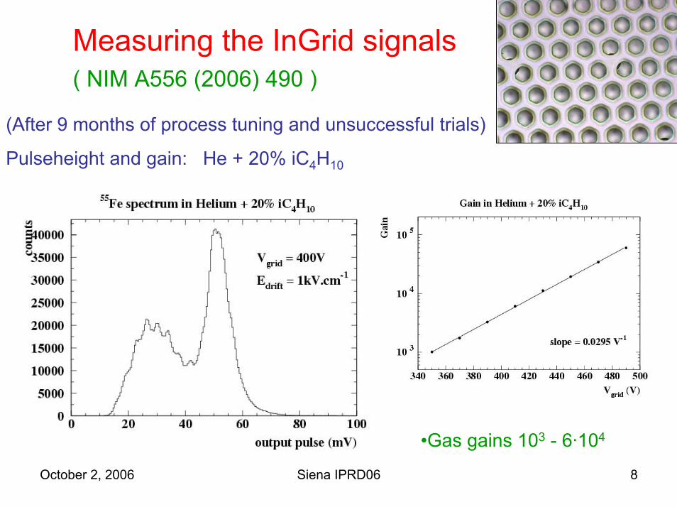
Measuring the InGrid signals ( NIM A556 (2006) 490 )
(After 9 months of process tuning and unsuccessful trials)
Pulseheight and gain: He + 20% iC4H10
•Gas gains 103 - 6·104

October 2, 2006 Siena IPRD06 9
Energy resolution in Argon IsoC4H10 80/20
•Observation of two lines:
Kα at 5.9 keV
Kβ at 6.4 keV
•Resolution σE/E = 6.5%
(FWHM = 15.3%)
•Gain variations < ±5%
•Photo peak asymmetry seen
•Very good energy resolution

October 2, 2006 Siena IPRD06 10
Gas gains in Argon
•Ar / CO2 mixtures offer good ageing properties
•Gain of 104 reachable in Ar / CO2 80/20
•Ageing studies in a reasonable amount of time (intense X-rays source)

October 2, 2006 Siena IPRD06 11
Any field structure feasible

October 2, 2006 Siena IPRD06 12
Gain for different gap sizesMaximum predicted in gain vs gap curve
deM α=
Gap (mm)
Y. Giomataris/N.I.M. A419 (1998) 239-250
0.001 0.01 0.1 11
10
1000
100
10000
Gai
n
V=400Volts
V=350Volts
V=300Volts
d gap thickness
p pressure
A,B depend on gasmixture

October 2, 2006 Siena IPRD06 13
Gain for different gap sizes• But now we can make measurements
Grid voltage
Gai
n
300 380 460 540102
103
104
105
Gap thickness (µm)35 45 6555 75
400V450V500V
75um35um55um40um

October 2, 2006 Siena IPRD06 14
Homogeneity• Gain measurements scanning the surface of the detector• Homogeneity given by grid quality
2.6 % RMS 1.6 % RMSx yyx
Gain Gain

October 2, 2006 Siena IPRD06 15
Simulated gain for different hole size• Electric field along z axis decreases with hole size• Different gain expected for different hole size
Hole size (µm)0 10 20 30 40
Gai
nGrid
400V 103
104
Z(µm)0 20 40 60 80
E(k
V.c
m-1
)
10
30
50
70 10µm hole
50µm hole
z = distance from anode

October 2, 2006 Siena IPRD06 16
Measured gain for different hole size
And measurements confirm simulationsG
ain
103
104
102
Vgrid460420 540500

October 2, 2006 Siena IPRD06 17
Energy resolution• Resolution depends on
– Primary,attachment,T,P– Collection efficiency (field ratio)– Gain homogeneity & transverse diffusion
103 10410
20
30
40
60
Res
olut
ion
(FW
HM
%)
Gain

October 2, 2006 Siena IPRD06 18
Resolution as function of gap
• Why a parabolic behavior ?
Vgrid
Res
olut
ion
(FW
HM
%)
20
30
40
50 35um55um75um
380 420 460 500
Gain
Energy resolution
F. Jeanneau et al. NIM A 461 (2001) 84–87
19
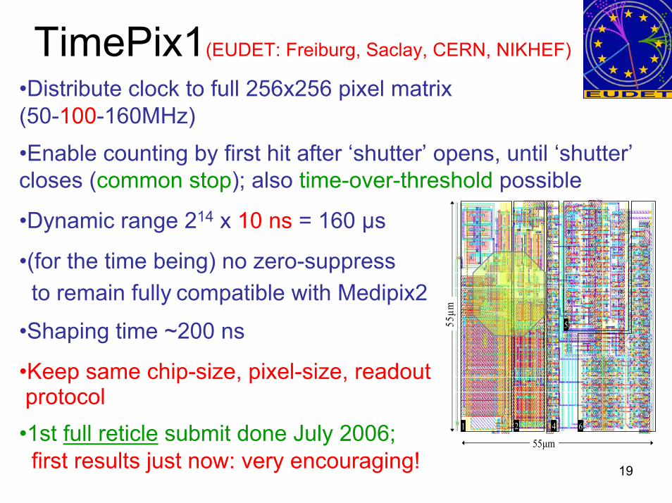
TimePix1(EUDET: Freiburg, Saclay, CERN, NIKHEF)
•Distribute clock to full 256x256 pixel matrix (50-100-160MHz)•Enable counting by first hit after ‘shutter’ opens, until ‘shutter’closes (common stop); also time-over-threshold possible
•Dynamic range 214 x 10 ns = 160 µs
•(for the time being) no zero-suppress to remain fully compatible with Medipix2
•Shaping time ~200 ns
•Keep same chip-size, pixel-size, readout protocol•1st full reticle submit done July 2006; first results just now: very encouraging!
11 22 44
55
66
55µm
55µm

October 2, 2006 Siena IPRD06 20
TimepixTimepix TOTTOT
17
100MHz 100MHz

October 2, 2006 Siena IPRD06 21
Timepix summary Timepix summary Physical dimensions 14.111 mm x 16.120 mm (like Mpix2MXR20)
Charge collection e-, h+
Linearity Up to 50Ke-
σ equalized ~25e-
Minimum Threshold ~500e- (expected)*
Max Analog power 6.5µW/pix 420mW/chip (@2.2V Vdda)Static Digital Power 440mW@100MHz (@2.2V Vdd)Readout Serial/ParallelReadout compatibility 95% (Clock active when shutter ON)
IO PADs 127 (like Mpix2MXR20)
Pixel functionality PhotonCounting, TOT, TimepixAmplifier Gain ~18mV/Ke-
Noise ~75e-
Thresholds 1 (4bits adj)
Counter Depth/Overflow 14-bits/Yes

October 2, 2006 Siena IPRD06 22
Sparking• Chip faces 80kV/cm with no protection (unlike
the GEM setup; 1.5 yr using same chip)• Degradation of the field, or total destruction
of grid but also CMOS chip
10µm

October 2, 2006 Siena IPRD06 23
CMOS Chip protection against - discharges- sparks- HV breakdowns- too large signals
Silicon Protection: SiProt
Amorph Si (segmented)
Empirical method:Try RPC technology

October 2, 2006 Siena IPRD06 24
- RPC principle: reduction of local E-field- Avalanche charge: electrostatic induction towards input pad- Specific resistance: - high enough to ‘block’ avalanche charge
- low enough to flow signal current- layer thickness 4 µm, Rvol = 0.2 GΩ/cm
TechnologyA-Si deposit possible in general; avoid wafers get too hot
Univ. of Neuchatel/IMT/P. Jarron (CERN) uses this forintegrated X-ray sensor/convertor on MediPix 2
--- -
plasma A-Si
Test: put Thorium in gas: Radon α-decays:- large (proportional) signals- Discharges: like short circuits

October 2, 2006 Siena IPRD06 25
UN
UN
UN
PROT
- no hot plasma onpixel input pads
- reduced charge & current
Looks like it works!
Discharge signals:short-circuit betweengrid and anodedue to plasma
PROT
PROT

October 2, 2006 Siena IPRD06 26
Alternative: TwinGrid

GOSSIP: Gas On Slimmed SIlicon Pixels(as a possible vertex/track detector at SLHC)
CMOS pixel array
MIP
InGrid
Drift gap: 1 mmMax drift time: 16 ns
MIP
CMOS chip‘slimmed’ to 30 µm
Cathode foil

October 2, 2006 Siena IPRD06 28
Sr-90 β-source
1.2 mm

October 2, 2006 Siena IPRD06 29
GOSSIPO-2
test of preamp-shaper-discriminator
+
700 MHz TDC per pixel
• 0.13 µm technology• containing 16 x 16 pixels• Submission Nov 2006• Can be used for GOSSIP demo!
•source capacity 15 fF
•peaking time 40 ns
•expected noise ~60 e-
•power: 2 µW/pixel

October 2, 2006 Siena IPRD06 30
Further DevelopmentsRELAXD project (Dutch/Belgian)
NIKHEF,Panalytical,IMEC,Canberra:• Chip tiling: large(r) detector surfaces
(2x2, 2x4 chips)• Through Si connectivity: avoiding bonding wires• Fast readout technology
(~5 Gb/s)

October 2, 2006October 2, 2006 Siena IPRD06Siena IPRD06 3131
GridPix: the electronic bubble chamber
NIKHEF Harry van der GraafJan TimmermansJan VisschersMaximilien ChefdevilleMartin FransenVladimir Gromov
Saclay CEA DAPNIA Paul Colas, David AttiééDan Burke,Yannis GiomatarisArnoud Giganon
Univ. Twente/Mesa+ Jurriaan SchmitzCora SalmVictor Blanco CarballoSander Smits
CERN Michael Campbell,Erik HeineXavi Llopart
Thanks to:Wim GotinkJoop Rovenkamp