Design Planning - Home - Lattice Semiconductor
52
Copyright © October 2013 Lattice Semiconductor Corporation. Design Planning Introduction FPGA design planning is done in two different phases of the FPGA design process: When you start your FPGA project – this is where you need to define your design’s functionality and the architecture, choose an FPGA device, and start writing the HDL code. During the FPGA implementation process – this is where you, as an FPGA engineer, target your design to the chosen FPGA device and decide how you want to utilize the chosen device Although these are two separate phases, refining one of them can significantly affect the other. For example, a design architecture change could include new functional blocks such as DSP or SERDES, which might require a new target device, and this can partially or completely invalidate the result of the second phase. On the other hand, in order to close timing, making some architecture or source code changes might be the quickest and easiest way to perform the second phase. This chapter focuses on the second phase and explains how you can fully utilize the functionality and features provided by Diamond to complete your design using Lattice FPGAs. The second phase also involves HDL coding and logic synthesis, which are explained in detail in separate documents.
Transcript of Design Planning - Home - Lattice Semiconductor

Copyright © October 2013 Lattice Semiconductor Corporation.
Design Planning
IntroductionFPGA design planning is done in two different phases of the FPGA design process:
When you start your FPGA project – this is where you need to define your design’s functionality and the architecture, choose an FPGA device, and start writing the HDL code.
During the FPGA implementation process – this is where you, as an FPGA engineer, target your design to the chosen FPGA device and decide how you want to utilize the chosen device
Although these are two separate phases, refining one of them can significantly affect the other. For example, a design architecture change could include new functional blocks such as DSP or SERDES, which might require a new target device, and this can partially or completely invalidate the result of the second phase. On the other hand, in order to close timing, making some architecture or source code changes might be the quickest and easiest way to perform the second phase.
This chapter focuses on the second phase and explains how you can fully utilize the functionality and features provided by Diamond to complete your design using Lattice FPGAs.
The second phase also involves HDL coding and logic synthesis, which are explained in detail in separate documents.

Design Planning in Diamond
2 Design Planning
Design Planning in Diamond
Design planning in Diamond is not mandatory for all designs, but it will be beneficial to most designs. This is especially true if the design is of medium or large size with high resource utilization or with a tight timing requirement. For these designs, design planning can help reduce potential timing issues or placement and routing problems, and it can increase the possibilities of design reuse and migration.
In Diamond, design planning should start as soon as possible, usually at the time when the logic synthesis has been completed successfully and the MAP process is ready.
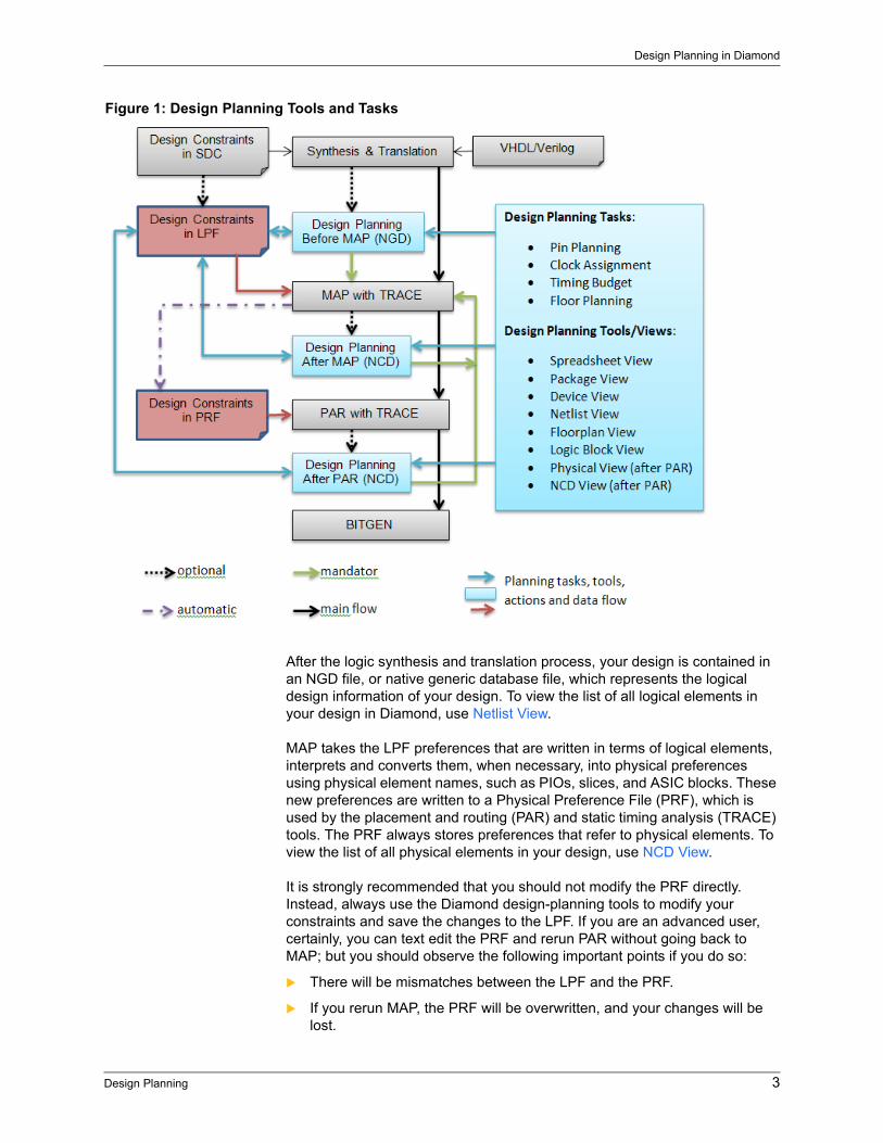
The diagram in Figure 1 illustrates the design planning flow within Diamond. It shows the places in the flow for design planning, the available planning tools, the tasks that can be performed, as well as the design data involved. From the diagram, notice the following important points:
The LPF, or logical preference file (with the file extension “.lpf”), holds all design planning constraints (called preferences) that drive the MAP and PAR processes (the engine).
Synthesis tools can optionally write out an LPF, which carries design constraints from the synthesis process. This LPF can optionally be used as your starting point.
After any design planning changes, which means LPF changes, the design flow is reset to the pre-MAP stage. This behavior suggests that although you can do design planning at any time, you should do it as early as possible, since MAP and PAR processes usually take most of the runtime in a complete flow iteration.
The MAP process maps the design component names, and certain design planning constraints/preferences defined in the LPF, from the logical domain to the physical domain. In the process, it automatically generates a PRF, or physical preference file. The PRF is used to drive the PAR process and its timing engine.
Preference Flow in DiamondAs illustrated in the diagram, in Diamond, all design constraints that drive the MAP and PAR processes are called preferences and are stored in a user-defined logical preference file (LPF), thus the implementation process is also called the preference flow.
The Diamond preference flow is designed to allow you to work with the FPGA design in terms of high-level logical elements, such as ports, nets, registers, instances, and any other special Lattice Semiconductor blocks derived from the RTL source through logic synthesis. The LPF is the primary interface for defining design-planning constraints, such as timing and location, in terms of logical elements.
Design Planning in Diamond
Design Planning 3
After the logic synthesis and translation process, your design is contained in an NGD file, or native generic database file, which represents the logical design information of your design. To view the list of all logical elements in your design in Diamond, use Netlist View.
MAP takes the LPF preferences that are written in terms of logical elements, interprets and converts them, when necessary, into physical preferences using physical element names, such as PIOs, slices, and ASIC blocks. These new preferences are written to a Physical Preference File (PRF), which is used by the placement and routing (PAR) and static timing analysis (TRACE) tools. The PRF always stores preferences that refer to physical elements. To view the list of all physical elements in your design, use NCD View.
It is strongly recommended that you should not modify the PRF directly. Instead, always use the Diamond design-planning tools to modify your constraints and save the changes to the LPF. If you are an advanced user, certainly, you can text edit the PRF and rerun PAR without going back to MAP; but you should observe the following important points if you do so:
There will be mismatches between the LPF and the PRF.
If you rerun MAP, the PRF will be overwritten, and your changes will be lost.
Figure 1: Design Planning Tools and Tasks

Design Planning in Diamond
4 Design Planning
There is no graphical view for modifying the PRF. You must use a text editor.
You need to fully understand the physical design data and the chosen device in order to make correct changes. All illegal constraints will be ignored by PAR, or they will cause PAR problems such as increased runtime and difficulties in fitting and routing the design. Illegal constraints might also stop the PAR process
Design Planning in the HDLYou can define certain design planning constraints in your HDL code using Lattice HDL Attributes and Directives. For definitions and explanations of all the attributes and directives supported by Diamond refer to the section “HDL Attributes” in the Constraints Reference Guide” of the Diamond online Help.
After logic synthesis, attributes and directives defined in your HDL code are written into the synthesis output database, usually in EDIF format. When the Diamond NGDBuild process translates the synthesis output and builds the Lattice design database (NGD, or Native Generic Database file), these attributes and directives are carried over into the NGD file, which will become part of your design planning constraints to drive the MAP and PAR processes. These constraints are visible in Lattice design-planning views, such as Spreadsheet View and Package View, but they are not present in the user-defined LPF. You have the opportunity to modify or overwrite these constraints in the design-planning views. After the changes in these views are saved, the new constraints will be written into the LPF, and they will overwrite those defined in the NGD.
Preferences and ProcessesThe MAP and PAR processes require effective constraints in order to optimize the usage of FPGA resources. For MAP and PAR, the design constraints, or preferences, are provided in an LPF file. You can set and edit design preferences at multiple points in the FPGA design flow.
Understanding Preferences (LPF)The LPF contains all the design constraints, including timing preferences that you specify for driving MAP and PAR using Diamond’s preference language. Although you can add or modify preferences before MAP, after MAP, or after PAR, the after-MAP or after-PAR changes effectively reset the flow, and changes must be implemented by rerunning the MAP and PAR processes
Design constraints can also be set by using attributes and directives in the HDL code. As explained previously, they are converted to EDIF properties by logic synthesis, and then carried over into the NGD database. They can then be viewed in Spreadsheet View or Package View. If the constraints are modified in these views, they will be included in the LPF, and these modified preferences will take precedence over the attributes in the HDL.

Design Planning in Diamond
Design Planning 5
MAP and LPFThe MAP process reads the LPF to map the logical elements. By default, the MAP process filters the preference file by ignoring any syntax errors or invalid preferences. Invalid preferences are preferences that do not correspond to any logical elements that are in the design. Invalid preferences are often caused by a typographical error in the element name; if you encounter such an error, use Netlist View as a reference to correct any error.
You can change the Map behavior so that it terminates and issues an error message whenever it encounters preference errors. To accomplish this, set the "Ignore Preference Errors" option to "False" in the Map Design section of the active strategy or use the -pe option from the command line.
The MAP process generates a physical preference file (or PRF, with file extension .prf), which carries all of the valid preferences contained in the LPF as well as all of the attributes that were included in the NGD through the HDL code (if they were not explicitly overwritten by the LPF). This PRF is used to drive MAP TRACE, PAR and PAR TRACE.
MAP TRACE, PAR TRACE and PRFAfter MAP or PAR, you have the option of performing static timing analysis on the physical design file (or NCD file, with file extension .ncd), which was generated by either MAP or PAR. Diamond’s static timing analysis tool, TRACE (Timing Reporter and Circuit Evaluator), takes the NCD and PRF as inputs and uses the timing constraints contained in PRF to produce a report file.
The MAP TRACE report file uses the file extension .tw1, it can be viewed in Diamond’s Report View or any text editor.
The PAR TRACE report file uses the file extension .twr, it can be viewed in Diamond’s Report View or any text editor.
PAR and PRFThe PAR process uses both location and timing preferences in the PRF to drive the placement and routing of the design. The output of PAR is a placed and routed design (an NCD file that is different from the NCD file generated by MAP), as well as a PAR report and an I/O pinout report file (PAD).
Recommendations for Creating and Editing the LPFCreating design preferences is a process that continuously evolves throughout the design process. Certain preferences are used during the MAP phase, and others are applied during PAR. Preferences are also used by reporting tools such as TRACE for static timing analysis to provide important information on the final design. It is very important to use appropriate and sufficient preferences.
Consider the following recommendations.

Design Planning in Diamond
6 Design Planning
Always Use Design Planning Tools Use Diamond’s Design Planning Tools to create, remove or modify your constraints to ensure the correctness. After changes are made and saved in these tools, your constraints will be written into the LPF automatically.
Text editing the LPF is only recommended for advanced users for reorganizing preferences in a user-friendly order, as explained in the following section. If you choose to text edit the LPF, you should also follow these recommendations to avoid potential problems.
Ensure a Clean Error-free LPFLPF is a “loose” language with very limited restrictions. It is able to accommodate human errors such as unrecognized preferences, syntax errors or semantic errors. Although there are certain DRC tools in Diamond such as PIO DRC that can prevent many of the I/O-related issues, some of the errors present in an LPF will only be caught by the MAP or PAR process. Most of time such an error will produce a warning message that the preference is being ignored, but there are times where the problematic preference will cause the engine to spend more time on unrealistic requirements or stop working. You should carefully examine any warning or error messages related to your LPF, and make sure that you correct problematic preferences as early as possible.
Preferences also constrain your design and the engine by using your design data, such as ports, nets, modules and instances. If your design’s source code has been changed and your design has been resynthesized, you should verify the correct use of your design data in your LPF to avoid semantic errors.
Ensure a Well-Organized LPFThe LPF written by design planning tools might not be well organized, depending on how you use these tools to create or change constraints. The general assumption is “first-created-and-saved, first-written.” You can reorganize the sequence of the preferences, as explained below.
An LPF can contain any number of preferences and any number of comments in any order. As your design process moves on, your LPF can become lengthy and less organized. Although this might not be a problem to the processing tools, it will get harder for you to manage and understand. Most importantly, it will get more difficult for you to correlate your constraints with the processing or analysis results. Here are some suggestions:
Create multiple sections, with each section covering one specific requirement area. For example, specific areas might include pin assignment, timing requirements, grouping, region assignments, IP-related.
Each specific area can be further divided into small groups. For example, for timing requirement, you might have groups such as clock-related, multi-cycle, and input setup.
Use comments to organize each section or group with descriptive information. You can use the pound sign (#) or double slashes (//) to start a comment line.

Design Planning in Diamond
Design Planning 7
Avoid conflicting preferences. Usually this is not a problem for Diamond (see Understand Precedence Rules for Preferences), but it could waste your time when you are debugging your design.
Put less specific preferences in front of more specific preferences in the LPF. For example, place global preferences before group preferences. This not only improves the preference coverage, but also helps constrain the items you really care about (see Understand Precedence Rules for Preferences).
Understand Precedence Rules for PreferencesObserve the following general precedence rules when setting preferences:
Preferences defined in an LPF take precedence over attributes and directives defined in the HDL code.
When IOBUF attributes exist in the .lpf file and in the HDL for the same port or port group, those in the .lpf file will completely override those in the HDL. Two exceptions to this rule are IO_TYPE and the placement constraint LOC.
All IOBUF attributes that exist in the HDL will get overridden by the Map process when the ALLPORTS attribute is used in the .lpf file.
Preferences that are more specific take precedence over less specific ones. For example, individual net or path preferences supersede group (bus) preferences, and group preferences supersede global preferences.
Preferences defined later in the LPF take precedence over those defined earlier, if these preferences are at the same level and are in conflict.
For timing preferences, different preferences have different precedence order. See the Timing Closure chapter for more details.
To illustrate, suppose that the LPF contains the following preferences:
MAXDELAY NET W 10 NS;
MAXDELAY ALLNETS 30 NS;
DEFINE BUS B NET Y NET Z;
DEFINE BUS A NET Y NET X NET W;
MAXDELAY BUS B 20 NS;
MAXDELAY BUS A 25 NS;
MAXDELAY NET W 15 NS;
Net W gets 15 ns because this preference is more specific than BUS A or ALLNETS, and it comes after the 10 ns preference. As a good practice, you should remove the 10 ns preference.
Net X gets 25 ns because the BUS A preference is more specific than ALLNETS.
Net Y gets 25 ns because the BUS A preference comes after the Bus B preference. As a good practice, you should not assign net Y to two different buses.
Net Z gets 20 ns because the BUS B preference is more specific than ALLNETS.
All other nets get 30 nanoseconds.

Design Planning in Diamond
8 Design Planning
For more details and examples of precedence rules, see the “Preference Conflict Resolution” section of Applying Design Constraints in the Diamond online Help.
Design Planning ToolsDiamond provides various tools for design planning. You should fully utilize the functions provided. These design-planning tools enable you to do the following:
View the design elements, in logical or physical domain, that you can manage
View the hardware resources that are available for the chosen device, such as pins, sites, and slices
Assign design elements to FPGA resources
View and modify your assignments
Examine how the resources are planned to be used (your constraints) and how the resources are actually used by your design (after PAR)
Identify any potential assignment problems, through the automated real-time PIO DRC check or the on-demand PIO DRC
Cross probe between different views. Cross-probing is very helpful for locating an assignment in different views and mapping logic elements to their physical counterparts.
Drag and drop between certain views to define constraints
Design Data LoadedAll design-planning views work directly on one, some, or all of the following types of design data:
Logical Preferences File (LPF) – This is where all of your constraints are written to drive the MAP and PAR processes. All constraint changes are written to this file, and whenever a change is saved, the flow is reset to pre-MAP stage.
Design data, which includes the following:
NGD file – The NGD file is only available and valid after a successful logic synthesis and translation process. This design data will be loaded before and after MAP. This implies that all design-planning tools are only available after a successful synthesis and translation process.
NCD database – There are two types of NCD databases: a mapped NCD and a placed and routed NCD. A successful MAP process produces the mapped NCD data, while a successful PAR process produces the placed and routed NCD data.
In Diamond, the mapped NCD is not loaded into the GUI. All design-planning tools load the placed and routed NCD data after the PAR processes finishes successfully.

Design Planning in Diamond
Design Planning 9
Design Views
Spreadsheet ViewSpreadsheet View is a tabular format, multiple-sheet tool for viewing, creating and editing design preferences in the logical domain. Spreadsheet View is the primary tool for pin planning and most other design constraining tasks. Spreadsheet View supports all preferences, including those editable in other views. The following sheets are available in Spreadsheet View:
Pin and Port assignments for assigning pin locations and other attributes such as IO type (IO standard), slew rate, and drive
Related preferences include LOCATE, IOBUF, BANK, and PROHIBIT.
Clock Resource for applying primary and secondary clock resources to clock domains in your design
Related preferences include USE PRIMARY (PURE/DCS), USE SECONDARY, PROHIBIT PRIMARY, and PROHIBIT SECONDARY.
Route Priority for assigning a PRIORITIZE preference to a net or bus with a weighted importance value (range from 0 to 100)
Cell Mapping for setting cell preferences of flip-flops in your design. Related preferences include USE DIN and USE DOUT.
Global Preferences for setting preferences that affect the entire design.
Related preferences include BLOCK, USERCODE, SYSCONFIG, SYSTEM_JITTER, TEMPERATURE, VOLTAGE, TRACEID, GSR_NET,
Timing Preferences for defining timing constraints, including BLOCK, FREQUENCY, PERIOD, INPUT_SETUP, CLOCK_TO_OUTPUT, MULTICYCLE, MAXDELAY, CLCKSKEWDIFF
Group for group definitions, including DEFINE GROUP and UGROUP
Miscellaneous Preferences for reserving resources, defining regions, setting Vref locations
Preferences include PROHIBIT SITE, REGION, LOCATE VREF.
Spreadsheet View also provides the following useful features:
Built-in real time PIO DRC that immediately validates your IO assignment
On-demand PIO DRC that validates your IO assignments and generates a DRC report
SSO analysis, based on your IO assignments
Pin migration display option that allows you to turn on or off the display of incompatible pins for pin migration purposes
Ability to export pin assignments to a pin layout file and exchange the assignment information with a third-party tool or PCB designers
Note
In Diamond, all user inputs and outputs are called ports and are listed in Spreadsheet View and Netlist View.

Design Planning in Diamond
10 Design Planning
Ability to import a modified pin layout file and update with assignments from an exported pin layout file
Ability to export a pinout file, which includes pinout information that is usually available from the Lattice website
Ability to add custom columns to the Pin or Port Assignments sheet and input user information related to a specific pin or port
Ability to include the custom column in an exported pin layout file
Ability to back annotate pin assignments produced by PAR to your LPF.
Figure 2 illustrates Spreadsheet View with a design loaded and with the Port Assignment sheet activated.
For more details about using Spreadsheet View, refer to “Using Diamond’s Preference Views”->”Spreadsheet View” in the Applying Design Constraints section of the Diamond online Help
For detailed descriptions of all preferences, refer to the “Preferences” section of the Constraints Reference Guide in the Diamond online Help.
Package ViewPackage View, shown in Figure 3, displays the color-coded pin layout of the selected device. It allows you to view, create, and modify pin location assignments. The color-coded layout indicates the types of pins, banks and other useful pin information.
Related preferences supported by Package View are LOCATE, PROHIBIT.
Note
The flow will be reset back to the pre-MAP stage if the back annotated assignments are saved.
Figure 2: Spreadsheet View Port Assignments Sheet

Design Planning in Diamond
Design Planning 11
Package View also provides the following features:
On-demand PIO DRC to check your pin assignments
SSO analysis
Display of incompatible pins for pin migration purpose
For details about using Package View, refer to “Using Diamond’s Preference Views”-> “Package View” in the Applying Design Constraints section of the Diamond online Help.
For detailed description of all preferences, refer to the “Preferences” section of the Constraints Reference Guide in the Diamond online Help.
Device ViewDevice View, shown in Figure 4 lists the hardware resources available for the chosen device. Based on the target device, the types of resources listed include PIOs and IOLOGIC sites, banks, DCS blocks, PFF and PFU slices, DQS, PCS, sysDSP, sysMEM, PLL/DLL and other embedded ASIC blocks.
Preferences supported by Device View include PROHIBIT.
Device View also provides the following feature:
On-demand PIO DRC, which generates a DRC report
Figure 3: Package View

Design Planning in Diamond
12 Design Planning
For details about using Device View, refer to the “Using Diamond’s Preference Views”> “Device View” in the Applying Design Constraints section of the Diamond online Help.
For detailed descriptions of all preferences, refer to the “Preferences” section of the Constraints Reference Guide in the Diamond online Help .
Netlist ViewNetlist View lists all of the logic design elements from the NGD database. The logic design elements are categorized and included in category trees of ports, instances or nets.
In the ports tree, you can assign ports to pins, create port groups, and define timing preferences. Related preferences include LOCATE, DEFINE GROUP, INPUT_SETUP, CLOCK_TO_OUT, FREQUENCY, PERIOD, MULTICYCLE and MAXDELAY.
In the instances tree, you can view logical instances in your design define GROUPs, and create UGROUPs.
In the nets tree, you can define timing constraints such as PERIOD, FREQUENCY and BLOCK preferences.
The images in Figure 5 show examples of Netlist View.
For details about using Netlist View, refer to “Using Diamond’s Preference Views” > “Netlist View” in the Applying Design Constraints section of the Diamond online Help.
Figure 4: Device View

Design Planning in Diamond
Design Planning 13
For detailed description of all preferences, refer to the “Preferences” section of the Constraints Reference Guide in the Diamond online Help.
Floorplan ViewFloorplan View displays the hardware resource locations of the chosen devices, including PIOs/IOLOGICs, sites and slices, and other types of resources such as sysDSP, sysMEM, depending on the chosen device.
Floorplan View allows you to view, create and modify certain design-planning constraints such as REGIONs, bounding boxes for UGROUPs and clock regions.
When PAR finishes successfully, you can also use Floorplan View to examine how your design is actually placed on the chosen device in term of pin assignments, slice utilization, etc. Floorplan View also supports the following features:
On-demand PIO DRC, with a generated report
Back annotation to the LPF file of various assignments made by PAR, including pins, sysIO buffer configuration, sysMEM EBR, sysDSP, and sysClock (PLL/DLL)
Access to Logic Block View after PAR, which displays the configuration and utilization of device resources
The images in Figure 6 show examples of Floorplan View after PAR.
For details about using Floorplan View, refer to “Using Diamond’s Preference Views->Floorplan View” in the Applying Design Constraints section of the Diamond online Help..
For detailed descriptions of all preferences, refer to the “Preferences” section of the Constraints Reference Guide in the Diamond online Help.
Logic Block ViewLogic Block View is a read-only view that displays the logic details of any placed and/or routed design component. Depending on the type of component selected, the view displays a tabular or schematic format.
Logic Block View is accessible from Floorplan View, Physical View and NCD View.
Figure 5: Netlist View – Port, Instances, and Nets Trees

Design Planning in Diamond
14 Design Planning
Other features supported by Logic Block View:
The ability to export a Logic Block View to a graphics file in a commonly used format, such as BMP and PNG.
The ability to use equations to view a block’s implemented logic
The images in Figure 7 show examples of Logic Block View after PAR.
For details about using Logic Block View, refer to “Using Diamond’s Preference Views > Logic Block View” in the Applying Design Constraints section of the Diamond online Help .
Figure 6: Floorplan View
Figure 7: Logic Block Views

Design Planning in Diamond
Design Planning 15
Physical ViewPhysical View is a read-only view that displays the detailed layout of your placed and routed design, including switch boxes and physical wire connections.
Physical View enables you to view various device elements and examine how your design was implemented by PAR. It also allows you to open Logic Block View for selected components to view the detailed implementations.
You can export the contents of a displayed Physical View to a graphics file in a commonly used format such as PNG and BMP.
The images in Figure 8 show examples of Physical View after PAR.
For details about using Physical View, refer to “Using Diamond’s Preference Views > Physical View” in the Applying Design Constraints section of the Diamond online Help.
NCD ViewNCD View is a post-PAR read-only view that provides an index of design elements for the chosen device, as well as resources that are used by the placed and routed design. All design elements are categorized in one of the two design trees: nets and instances.
NCD View enables you to select assigned sites for defining a UGROUP and takes you to Spreadsheet View for the definition. NCD View also allows you to open Logic Block View for a selected element.
Figure 9 shows an example of NCD View after PAR.
For details about using NCD View, refer to Using Diamond’s Preference Views > NCD View in the Applying Design Constraints section of the Diamond online Help.
Figure 8: Physical View

Design Planning in Diamond
16 Design Planning
Cross-Probing between ViewsCross-probing between design-planning views allows you to cross-reference a logical or physical design element or device element from one view to another. It very helpful for understanding the resources available in the chosen device, and it enables you to view, create, and define constraints, map a logic element to its physical counterpart, and examine the resource usage related to your design constraints.
When using the cross-probing feature, you can split or undock selected design-planning views and place them side-by-side for better viewing.
The following examples describe some of the usages.
Pin/Port Cross ProbingTo cross-probe a pin or port between different views, right-click a selected pin or port, and then choose Show In from the context menu.
This is useful for finding out where an assigned pin is located on the device. Figure 10 shows an example of the context menu in Spreadsheet View’s Port Assignments sheet. From here, you can cross-probe to Package View, Device View, Netlist View, NCD View (if after PAR) and Floorplan View.
Net Cross-ProbingNet cross-probing, which is available after PAR, enables you to cross-probe a net between Netlist View, Floorplan View and Physical View. To cross-probe a net between different views, select a net and choose Show In from the context menu. The net will be highlighted automatically in the selected view.
Net cross-probing enables you to examine a net’s connections in Floorplan View and Physical View, and it shows how a net travels through switch boxes in Physical View. For example, in Netlist View, right-click a net, and choose Show In from the context menu, as shown in Figure 11.
Figure 9: NCD View

Design Planning in Diamond
Design Planning 17
Then you can cross-probe to Floorplan View or Physical View, as shown in Figure 12.
Figure 10: Pin/Port Cross-Probing
Figure 11: Cross-Probing from Netlist View
Figure 12: Cross-Probing to Floorplan View and Physical View

Design Planning in Diamond
18 Design Planning
Instance Cross-ProbingInstance cross-probing, which is available after PAR, enables you to cross-probe an instance between Netlist View, Floorplan View, NCD View and Physical View. To cross-probe an instance between different views, right-click the instance and choose Show In from the context menu The instance will be highlighted automatically in the selected view.
Cross-Probing Between Logical and Physical DomainsInstance cross-probing is very useful for matching element names between logical and physical domains. Select an element in Netlist View and cross-probe to NCD view, or vice versa.
Instance cross-probing also enables you to find out what logical elements were packed into a slice or a group of slices. Select one or more slices in NCD View and cross-probe to Netlist View. To find out where a logical element was packaged into which slice, select the logical element in Netlist View and cross-probe to NCD View, as illustrated in Figure 13.
You can also cross-probe to Floorplan View or Physical View to locate the instance on the device, and then open Logic Block View to examine the details of the implementation.
For further information about supported cross-probing features, refer to “Using Diamond’s Preference Views > Cross-Probing Between Views in the Applying Design Constraints section of the Diamond online help.
Auto-HighlightLogic Block View and Physical View support auto-highlighting between the two views. To highlight an element, simply select it in one view and it will be highlighted in the other view automatically, as shown in Figure 14.
Figure 13: Cross-Probing Instances from Netlist View to NCD View

Pin Planning
Design Planning 19
Common DatabaseIn general, all the design-planning views share the same common database, such as LPF, NGD, or NCD, if they are relevant. Assignment changes in one design view are loaded immediately into the other open related views, and they will be loaded into other related views as soon as you open them.
If changes have been made but not saved, all relevant open and non-read-only views will indicate this status with an asterisk in the title bar. Even when all views are closed, the changes are still in the common database loaded in memory. The changes will only be written into the LPF file when you use the Save command.
Pin Planning
IntroductionPin planning is the process of defining your FPGA I/O protocols and locations on the chosen device. It is based on your actual design and the chosen device. In Diamond, the pin planning process involves the following tasks:
1. Assign your design ports to I/O locations on the chosen FPGA device.
2. Define the I/O protocol, (IO Standards, or IO TYPE in Diamond) and other I/O characteristics, such as slew rate, based on your design requirements.
3. Check your assignments for legal usage of the target device’s pins.
4. Validate and review your constraints and the actual usage through the MAP and PAR processes, and then refine the assignments.
5. Exchange your pin assignments with other parties, such as PCB schematic and layout designers for system integration.
Figure 14: Auto-Highlighting in Logic Block View and Physical View

Pin Planning
20 Design Planning
6. Document your final assignments.
PIC, PIO, IOLOGIC and sysIOA Lattice FPGA contains multiple programmable interface cells, or PICs. For ECP3 devices, each PIC contains two programmable I/O cells, or PIO cells, namely PIOA and PIOB. For different devices, each PIC may have different number of PIO cells.
I/O BanksThe sysIO buffers on a device, and PIOs connected to them, are arranged in groups, or I/O banks. Different devices have different numbers of I/O banks and might arrange I/O banks differently on the device.
Usually a device provides a number of user I/O banks and, optionally, configuration I/O banks. User I/O banks contain user I/Os (or user pins) for your design’s input and output usage (in Diamond, your design’s inputs and outputs are called ports). While the configuration I/O bank has dedicated and shared package pins for configuration, these shared pins become available as user I/Os when they are not used for configuration.
Each I/O bank has its own I/O supply voltage (or VCCIO) through a dedicated pin. In addition, user I/O banks usually provide voltage reference pins, also called VREF pins. These pins are completely independent from each other. A VREF pin is required for reference voltage in banks that contain I/O assignments of certain types, such as HSTL or SSTL.. If a reference voltage is not required, you can use these VERF pins as regular user I/Os.
Banking SchemeBanking scheme refers to how I/O banks are arranged on a specific device, and it refers to each I/O bank’s characteristics and features. Different devices usually have different banking schemes. Refer to the device’s documents for complete information.
I/O TYPEDifferent devices often support different I/O types, and you should check the devices documents for complete information. Commonly supported I/O types include:
Single ended: LVTTL 3.3V, LVCMOS 1.2V, 1.5V, 1.8V, 2.5V and 3.3V
Single ended requiring VREF: SSTL and HSTL
Note
Different devices might have different PIO characteristics. For detailed and accurate technical specification of I/Os for each device, refer to the related device handbook, datasheet, white papers and technical notes.

Pin Planning
Design Planning 21
Differential: such as LVDS, BLVDS, LVPECL, MLVDS, RSDS, differential SSTL, differential HSTL, etc.
True and Emulated LVDS I/OsCertain devices, such as LatticeECP3 devices, support both “true” LVDS I/O and “emulated” LVDS I/O. You can use both directly as LVDS inputs, and you can use true LVDS I/O as LVDS outputs. If you use emulated LVDS I/O as LVDS outputs, you need to pay additional attention and add external termination resistors. See the technical note TN1177 “LatticeECP3 sysIO Usage Guide” for additional information.”
Dedicated Hardware Circuit Pins
SERDES/PCSA SERDES, or serializer and deserializer, is an integrated circuit transceiver that converts serial data to parallel data and parallel data to serial data. In Diamond, PCS SERDES, or physical coding sub layer SERDES, is the same as SERDES.
Certain high-end devices might include one or more dedicated on-chip SERDES circuits, or channels. Each SERDES channel has its dedicated transmit and receive pins as well as the clock pin.
PLL/DLLLattice FPGAs include dedicated PLL and/or DLL circuits on chip. These circuits have their dedicated pins, which can be used as regular I/Os if not used for PLL/DLL purposes.
DQSSome Lattice FPGAs include pins that are DQS-capable. DQS is a bidirectional data strobe signal used by the DDR interface in an SDRAM for high-speed operation. These pins can be used as regular I/Os as well.

Pin Planning
22 Design Planning
Preferences for Pin PlanningTable 1 lists all preferences related to pin planning. These preferences can be defined in Diamond’s Spreadsheet View or by text editing the LPF file.
Design Views for Pin PlanningThe pin planning task involves various design views. Spreadsheet View is the most commonly used editor for this task, because it covers all pin-related preferences. Other views that can be used for pin planning are Package View, Netlist View, Device View, and Floorplan View.
The following design view features can help you with pin planning:
Display of default values in Spreadsheet View
Default values are the default I/O attributes used by Diamond when values are not provided by the user. For example, if you do not define an I/O Type for a port, Diamond uses the default “LVCOMS25” for most Lattice devices.
By default, default values are shown in the Port Assignments sheet of Spreadsheet View. You can use the View menu to turn the display of default values on or off. Default values are show in the default blue color, and you can change this by using the Tools > Options dialog box.
NGD and LPF locked value
Table 1: Pin Planning Preferences
Type Name Purpose Example
Locations
BANK Set a bank’s VCCIO value; Only compatible and unassigned ports will be assigned to the bank by PAR using the I/O placer algorithm.
BANK 2 VCCIO 2.5V;
LOCATE Assign a port to a pin. LOCATE COMP “clk” SITE “A1”;
LOCATE VREF Assign a voltage reference to a VREF pin.
LOCATE VREF “vref1_bank3” SITE “N21” IOTYPE “SSTL18_I”;
PROHIBIT Prevent a pin from being assigned by PAR.
PROHIBIT SITE “A1”
I/O Attributes
IOBUF Set a port or a port group or all ports’ I/O attributes such as IO_TYPE, DRIVE, SLEWRATE.
IOBUF PORT clk IO_TYPE=LVTTL33 DRIVE=8;
SYSCONFIG Defines system configuration settings for sysCONFIG ports,
SYSCONFIG CONFIG_MODE = SLAVE_SERIAL PERSISTENT = OFF DONE_OD = ON;
Misc.DEFINE GROUP
Create a port group for group assignment; for example, assign a port group to a bank.
DEFINE PORT GROUP “mybus” “a_2” “a_1” “a_0”
Pin Planning
Design Planning 23
An NGD locked value is an I/O attribute that has been defined in your HDL code using Lattice Attributes or Directives (as explained in the sections “Design Planning in the HDL” on page 4 and “Understand Precedence Rules for Preferences” on page 7). The attribute is then carried over to the NGD database after logic synthesis and translation.
An LPF locked value is an I/O attribute that was defined in the LPF file, or that was defined using Diamond’s design views and tools and then saved in the LPF file.
In Spreadsheet View, an NGD locked value is displayed in dark green by default, and an LPF locked value is displayed in black.; You can use the Tools > Options dialog box to change these default colors.
Display of differential pin pairs, banks, etc, in Package View.
Package View allows you to view pin locations and other information such as differential pairs, banks, DQS group and SSO. You can turn the display of these features on or turn off for easy planning.
Pin migration
Pin migration information in Spreadsheet View and Package View enables you to examine pins that are incompatible between different devices of the same package type and device family. This can assist you in making pin assignment decisions. Large devices (with more LUTs) usually have more user-assignable pins then small ones. If you need to migrate to a large or small device in the future, this feature will help you avoid using incompatible pins. See the section “Pin Assignment Exchange” on page 30 for more details.
Pin AssignmentPin assignment is an important aspect of design planning, especially for large designs that use large amount of I/Os with complex I/O banking rules, clocking, and special hardware features such as SERDES, and PLL.
General ConsiderationsYou should consider various facts before making any pin assignments. Assuming that the target device has been selected and that the available pins are sufficient for your design, your considerations should include, but not be limited to the following:
General I/O assignment, including pin locations (left, top, right, bottom,) and distances to the driving/driven logic related to your floor plan, if there is any
PCB board design and the surrounding components to which the FPGA connects
Availability of general PIO features such as IO Standards, banking rules, clocking resource, dual function pins, and dedicated pins
Specific silicon features and related pins such as SERDES, PLL/DLL, if applicable

Pin Planning
24 Design Planning
Common PracticeThe general steps toward successful pin assignment include the following:
Make sure that all or most of your design I/Os are defined at the front. Complete design I/O definition helps foresee the big pin-planning picture, and it will limit unnecessary replanning tasks and reduce core processing iterations in the future.
Plan ahead with board designs to lock down approximate I/O locations based on the board layout. Use a Diamond pin layout file to exchange pin assignment information.
If device migration needs to be considered for the future, use the Diamond pin migration features provided in Spreadsheet View and Package View.
Pre-assign all the resource-dedicated pins such as clock, PLL, DDR, and SERDES.
If possible, lock general-purpose I/Os to banks instead of specific pins. This gives the MPAR engine the most flexibility in placing and optimizing design logic.
Run PIO DRC in Spreadsheet View and Package View to identify any potential issues as early as possible.
Optionally, use the I/O Assistant strategy for a quick I/O validation.
Optionally, run I/O Timing Analysis, examine the I/O timing report, and make appropriate adjustments.
Optionally, back annotate pin assignments to the LPF as constraints for driving MPAR when the design logic is complete.
Port-Centric AssignmentThe port centric pin assignment approach is a method in which you first select a port or a group of ports (your design’s inputs and/or outputs), and then you complete one or both of the following tasks:
Task1: assign the ports to device pins
Task2: define port attributes, such as IO TYPE, bank location, slew rate, and drive
The port-centric approach is recommended for Task2, defining port attribute, because most of a design’s I/O features and attributes need to be defined through ports. This can be accomplished in the Port Assignment sheet of Spreadsheet View.
For details about using Spreadsheet View, refer to “Working with Preference Sheets” in the Applying Design Constraints section of the Diamond online Help.
For Task 1, to assign ports to device pins using the port-centric approach, you can use Spreadsheet View and Netlist View. Simply select a port or a group of ports, right-click, and choose Assign Pins from the context menu. This opens the Assign Pins dialog box for assigning ports to pins.

Pin Planning
Design Planning 25
Handling Differential PortsDiamond supports two methods for defining a differential port in your design:
1. Directly instantiate a differential I/O buffer in your HDL code.
For example, ILVDS buffer. With this method, you need to define a differential pair using two I/Os in your HDL, and connect them to the buffer. Spreadsheet View will then show the signal connected to the positive pin of the buffer, and you will see that the I/O Type has been assigned to the differential type automatically. The negative signal of the pair will not be listed. The following VHDL example includes a port definition (clk and clk_n in this case). It is illustrated in Spreadsheet View in Figure 15 .
ILVDS_INST: ILVDS port map(AN=>clk_n, A=>clk, Z=>clk_o);
This demonstrates that a pin assignment to a differential pair is made to the positive port. A pin assignment to the negative port is not allowed; this will be done automatically by the MAP and PAR processes. If you have a negative port assignment to a pin in your LPF, it will be flagged as an error and ignored by Diamond. In addition, if the positive port is assigned to a pin and the negative complementary pin is occupied by another port, this will be flagged as an error by PIO DRC.
2. Assign a differential I/O Type to the port listed in the Port Assignments sheet of Spreadsheet View. The Port Assignment sheet lists all of the design’s inputs and outputs that are defined in your HDL code (except the negative port of a differential pair defined using an instance of a differential buffer, as explained previously). If you need to define a port as differential, assign a differential IO Type to the port in Spreadsheet View.
Pin-Centric AssignmentThe pin-centric assignment approach is a method in which you first select a pin, and then you assign the pin to an input or output port of your design. The pin-centric approach only allows you to assign a selected pin to a port. To define a pin’s characteristics, such as I/O Type, you need to assign the pin to a port, and then define those characteristics for the port using the Port Assignments sheet in Spreadsheet View, as explained in “Port-Centric Assignment” on page 24.
Pin-centric assignments can be made in the Pin Assignment sheet in Spreadsheet View.
Figure 15: I/O Type in Spreadsheet View

Pin Planning
26 Design Planning
Other Pin Assignment MethodsBesides the port-centric and pin-centric approach, you can also use the following methods to make or change a pin assignment:
In Package View, drag a pin (source pin) that has been assigned and drop it to another assignable pin (target pin) to make a change. If the target pin has not been assigned, the port assigned to the source pin will be reassigned to the target pin, and the source pin will be released. If the target pin has been assigned, a dialog box will open that enables you to confirm the assignment swap or cancel the operation.
Drag a port from Netlist View and drop it to an assignable pin in Package View, or drop it to a pin in the Pin Assignments sheet of Spreadsheet View
To remove a pin assignment in Package View or Netlist View, right-click an assigned pin or port, and then select Unlock from the context menu. To remove a pin assignment in Floorplan View, right-click the assigned site and clear the Set Locate Preference selection from the context menu. To remove a pin assignment in Spreadsheet View, right-click the assignment and select Clear from the context menu. Note that the “Clear” command in Spreadsheet View not only removes the pin assignment, but also clears all other user-assigned attributes.
Dedicated Hardware Resource Pin AssignmentMore advanced FPGA devices, such as the LatticeECP3, provide dedicated hardware resources. For example, PLL, SERDES, and DDR2/DDR3 interface.
Dedicated hardware features are required to be locked down to certain locations on the device. If you have not locked down the locations, usually PAR will automatically assign the locations and generate a pinout file (the PAD file). Because there are multiple dedicated hardware locations, sometimes making these assignments can improve your design’s performance.
For a dedicated hardware resource, instead of assigning its pins, you usually assign the hardware resource instance to a dedicated resource location by text editing the LPF file. For example, the following LOCATE preference assigns a PLL instance to a PLL resource that is available on an ECP3 device:
LOCATE COMP “PLL_0/PLLInst_0” SITE “PLL_R35C70”;
The dedicated pins for this particular PLL resource will be used and assigned automatically by PAR, according to this PLL resource assignment.
The example below shows how a PCS instance is assigned to a PCS resource available on an ECP3 device:
LOCATE COMP "pcs_inst_name" SITE "PCSB";
Again, PAR will automatically assign this PCS resource’s pins to this PCS instance.

Pin Planning
Design Planning 27
On the other hand, you are certainly allowed to specify pin locations for some of the hardware resource instances, but special attention must be paid. For example, LatticeECP3 devices have the following limitations for designs that include DDR:
ECP3 devices do not provide DDR functions for the pins on the bottom edge of the device, so you should not assign a DDR interface to the pins on the bottom.
ECP3 devices do not allow 2x gearing ODDR on the top edge, so you should not assign a DDR3 interface to the pins on the top.
Since different FPGA architectures have different hardware resources, you should refer to the related datasheet, application note, or technical note for details on how to assign these resources.
Identify hardware resources used in your designThe first step in assigning a hardware resource location is to find out which hardware feature is used in your design. You can easily do this by viewing the “ASIC Block” in Netlist View. In the sample design shown in Figure 16, a PLL is used.
To capture the instance name accurately, you can simply select the instance in Netlist View and use the Ctrl+C keyboard shortcut. This will copy the complete name, in this case “i_my_pll/PLLInst_0”. Paste it into the LPF to create a LOCATE preference.
Identify hardware resources available on the target deviceThe second step in assigning a hardware resource location is to find out the available hardware resources on your chosen device, their identities, and locations.
You can identify available hardware resources in Device View. The example in Figure 17 shows that the target device has four PLLs built in.
You can use the cross-probing feature to view the locations of these PLLs on the device, as shown in the Floorplan View image.
Figure 16: ASIC Block in Netlist View

Pin Planning
28 Design Planning
To capture the hardware resource name accurately, select it in Device View, use the Ctrl+C keyboard to copy it, and then paste it into the LPF to create a LOCATE preference.
Pin MigrationOften when you start pin planning, you want to consider the possibility of retargeting your design to a device with larger or smaller capacity of the same package and device family. There are various reasons for considering this. You might want to reduce cost by choosing a small device, or you might want to migrate to a large device for future function expansion. The pin assignments, though, should stay the same or require minimum changes in order to avoid PCB redesign.
Diamond provides a pin migration feature that allows you ensure the pin assignment compatibility between different devices of the same package in the same device family. This feature enables you to do the following:
View incompatible pins in Spreadsheet View and Package View
Disable incompatible pin assignment in both views
Prevent MAP and PAR from using incompatible pins by adding a PROHIBIT preferences to those pins, using Spreadsheet View or Package View
Export pin migration information to a Pin Layout File, a CSV-formatted file that includes all package pins and their related usage information
For details about using the Diamond pin migration feature, refer to “Migrating Pin Assignments” in the Applying Design Constraints section of the Diamond online Help.
For more information about the pin layout file, refer to the section “Pin Assignment Exchange” on page 30.
Figure 17: PLL Resource in Device View and Floorplan View
mp

Pin Planning
Design Planning 29
PIO DRCDiamond provides PIO design rule checking (DRC), which enables you to validate I/O placements and attribute assignments.
PIO DRC works in two modes: real time check and on-demand check.
Real-time check
Real-time check is performed each time you make pin-related assignments or modifications in the Port Assignments or Pin Assignments sheets of Spreadsheet View. Any unconditional error will be rejected, while a conditional error will be accepted but flagged. Appropriate error or warning messages are displayed immediately in the Output window. An unconditional error is caused by an illegal assignment, where the assignment cannot be corrected by making any other related modification. For example, if you assign a port to a non-existing pin or to a non-user pin such as an NC (Not-Connect) pin, the error is unconditional.
A conditional error is caused by an assignment that makes the current combination of a port’s attribute definitions illegal, but where the illegal combination state can be corrected by making some other related modifications. Most legal combination rules are defined in the Legal Combination Table, which is predefined by the target device.
On-demand check
On-demand check is performed whenever you use the Preference PIO DRC command. It is also performed automatically by Diamond when you save your pin assignment changes. On-demand check covers most of the same checks that are performed by real time check, but it looks at the overall picture, examining all pin-related constraints for the chosen device, and making sure that there are no conflicts or errors. For example, it will catch an illegal mixing of VCCIO voltage requirements for a single bank.
You can run on-demand check from Spreadsheet View, Package View, Floorplan View and Device View.
PIO DRC can catch many common errors and prevent wrong pin usage at the early stage of the design process before you spend time running MAP and PAR, whose runtimes are usually very long.
To tape out your final pin assignment, you should use the results from a successful PAR, or use the I/O assistant strategy and flow, as explained in the section I/O Assistant Strategy.
I/O Assistant StrategyThe I/O Assistant strategy is a pre-defined strategy that allows you to run through MAP and PAR quickly to place I/Os and verify that your pin constraints, if any are legal. When the PAR process finishes successfully without any error or warning messages related to your pin assignments, the final I/O placement is assumed to be legal, whether constrained by you or auto-placed by the MAP and PAR processes.

Pin Planning
30 Design Planning
The I/O Assistant flow runs the logic synthesis, translation and MAP processes normally. For PAR, it only runs I/O placement, which avoids the long PAR runtime for placing and routing your whole design. When using the I/O Assistant strategy, note that the final NCD file generated by PAR will be incomplete and should not be used for generating the bit stream file or exporting a JEDEC file.
To use I/O assistant strategy, simply set it as the active strategy for an implementation.
I/O Assistant Strategy with Incomplete DesignThe I/O Assistant strategy can be used with a design that is not fully completed. This is very useful during the early pin planning process, where you only need to define the top-level inputs and outputs; for example, the top-level VHDL Entity only.
When using the I/O Assistant strategy with an incomplete design, you should make sure that the top-level ports will not be “optimized” away by the logic synthesis process. Where only top-level ports are defined, you should use the appropriate synthesis attributes and head files. For detailed information, refer to “I/O Assistant Design Entry” in the Diamond online Help.
Pin Assignment ExchangeExchanging pin assignment information with a third-party person or a third-party tool is a common practice in FPGA design. For example, you might need to export your pin assignments to a file and hand it over to a board designer for schematic capture or PCB layout. The board designer can then modifies the pin assignments, update the file, and hand it back to you to update the pin assignments in Diamond.
You can export a pin layout file in Diamond. A pin layout file is a text file that contains all the pins of your target device and -- depending on the process stage the pin usage information, such as port assignments and attributes definition such as IO Type and slew rate.
For detailed information about the pin layout file, refer to application note AN8087, which is available on the Lattice website.
Export Final Pin AssignmentsIn typical usage, the final pin assignments are exported for the PCB design. This is done after PAR has finished successfully. To export the final pin assignments, open Spreadsheet View and choose File > Export > Pin Layout File. The Pin Layout Export dialog box opens, as shown in Figure 18.
All the fields that can be exported are optional, and you can select those that you want included in the pin layout file. You can also change the order in which the fields are displayed, select the delimiter and specify a name for the

Pin Planning
Design Planning 31
exported file. Note that all pins, including non-user pins such as NC pins, are exported.
For PCB design purposes, you should at least include the following fields: pin number, signal name, and direction.
You can also include any custom columns that were created in the Port Assignment or Pin Assignment sheets of Spreadsheet View. Custom columns are helpful for entering design-specific pin information. For example, you could give all pins that would be on one schematic symbol the same value under a custom column called “symbol.”
Import Pin Assignment ChangesPCB designers can make pin assignment changes directly to an exported Pin Layout File. Certain PCB design tools, such as Mentor Graphics PADS, can also export pin assignment to a CSV-formatted file. The changes can then be imported into Diamond through the File > Import > Pin Layout File command, which opens the dialog box shown in Figure 19.
When importing a modified pin layout file, make sure that the file header and column names are not changed. The following example shows the header and column names from an exported pin layout file.
Figure 18: Pin Layout Export Dialog Box

Pin Planning
32 Design Planning
#Pin Layout Report file generated by Lattice Diamond Version 1.4#Generated at Mon Oct 31 15:03:17 2011#DESIGN = diff_d#DEVICE = LCMXO2-1200HC#PACKAGE = TQFP144#SPEEDGRADE = 6Pin_Number,Pad_Name,Function,IO_Bank_Number,Signal_Name,Direction
Similarly, when importing a CSV file exported by a third-party PCB design tool, it is recommended that you include the header and column names in the file, as shown in the example. At a minimum:
The column names should follow the naming convention used in the pin layout file.
The Pin_Number and Signal_Name columns must be included in the file in order for the pin assignment changes to be imported.
Examine the Final Pin AssignmentIf PAR finishes successfully, you will have the final pinout of the design. There are a few ways to examine the final pinout in Diamond:
In Spreadsheet View, select Display IO Placement from the View menu. This command displays the final pin placements in parentheses, as illustrated in Figure 20.
Figure 19: Import Pin Layout File Dialog Box
Figure 20: IO Placement in Spreadsheet View

Pin Planning
Design Planning 33
Similarly, in Package View, select Display IO Placement from the View menu to display the final pin placement, as shown in Figure 21.
The final pinout can also be viewed in NCD View, Floorplan View and Physical View.
A PAD file is automatically generated after PAR. This file includes all the I/O usage information, it can be viewed in Report View.
If you need to examine a specific pin’s usage, you can open Logic Block View for the selected pin, as shown in Figure 22. Logic Block View of a specific pin is available in NCD View, Floorplan View and Physical View.
Figure 21: IO Placement in Package View
Figure 22: Pin Usage in Logic Block View
Clock Assignment
34 Design Planning
In addition, a final pinout can be exported to a pin layout file for documentation purposes.
Clock AssignmentLattice FPGAs have dedicated clock resources that are optimized for fast clocking and have minimum skews. The use of dedicated clock resources helps avoid timing or other issues, and it frees general routing resources for other design purposes.
Clock ResourcesDepending on the target device, Lattice FPGAs provide one, some, or all of the following types of clock resources:
Primary clock resources -- These are the global clocks with dedicated routing resources distributed across the whole chip. Primary clock resources are also quadrant-based.
Secondary clock resources -- These are flexible clock resources and are optimized for large fan-outs and minimum skew. The secondary clock can be used as a clock, a clock enable, or a set/reset that requires large fan-outs.
Edge clock resources -- These clocks span through part or all of the I/O rings on the left, right, top or bottom side of a device. Edge clock resources have low injection time and skew, and they are used to clock I/O registers. Edge clocks are designed for high-speed I/O interfaces with high fanout capability. They can directly drive the secondary clock resources and general routing resources, and they might drive the primary clock resources through other blocks such as CLKDIV.
Quadrant clocks -- A primary clock can be split into four quadrant clocks. A quadrant clock can be used as a clock residing in the quadrant on the device. Each quadrant clock can be independent from other quadrant clocks or tied to other quadrant clocks in the adjacent quadrants. Some quadrant clocks also provide the Dynamic Clock Selection (DCS) feature.
Secondary region clocks -- These are clocks that are optimized locally for local regions where secondary region clocks operate. Using a region clock can minimize the clock skew in the region.
In addition to these clock resources, Lattice FPGAs can also include clock input pins, PLLs, DLLs, DCSs, and clock dividers.
Some Lattice FPGAs support the use of general routing resources for clocks. General routing resources are optimized for data routing and will not have the same performance and low skew as the dedicated clocking resources, so they are not recommended for routing clocks.
For detailed information about the clock resources available in your chosen device, refer to the related sysCLOCK design guide, application note, or technical note.
Clock Assignment
Design Planning 35
Using Clock Resources
General ConsiderationsWhen doing clock planning, speed (or clock frequency) and clock fan-out loads are the main concerns. An FPGA’s total number of available clock resources is also a deciding factor.
To ensure a successful clock assignment, you need to understand the requirements and clock resources available. Consider the following numbers before clock planning:
The total number of clocks required for your design and the number of loads for each clock
One way to find out these two numbers is to examine the Design Information section of the MAP report. For example:
Design Information......Number of clocks: 2 Net clkok_c: 17 loads, 17 rising, 0 falling (Driver: i_my_pll/PLLInst_0 ) Net clkop_c: 17 loads, 17 rising, 0 falling (Driver: i_my_pll/PLLInst_0 )......
The total number of clock resources available from the target device
The frequency requirement for each clock
When there is no user preference, the engine uses clock loads as the criteria for automatic clock resource assignment. This behavior can be overwritten by user constraints. Consider the following when defining clock constraints:
In general, use the primary clock resource for the clock that runs at the highest speed and/or has the highest fan-outs.
When more primary clock resources are required than are available on the target device, consider using a quadrant clock if the fanout and the placement of these clock resources are practicable. This might require a few processing iterations to yield an optimal quadrant clock assignment. Note that using quadrant clocks will effectively constrain the placement of certain sequential elements driven by the quadrant clock, which can stress the placement and routing. Therefore, it could affect the timing result of your design, especially with the cross-domain elements that are related to the clock.
If more secondary clocks resources are required than are available on the target device, consider using secondary region clock resources. Consider that the secondary regional clock resources differ between different devices. For some device families, the secondary regional clock is unavailable or not fully supported. Make sure that you understand your target device’s capability.

Clock Assignment
36 Design Planning
Use edge clock resources for high speed I/O interfaces. Also, if CLKDIV is used in your design, it should be driven by an edge clock to ensure a synchronous transfer in the I/O logic.
Dedicated Clock Resources vs. General Routing ResourcesIn rare cases, you might use the general routing resources for a clock; for example, for a very small clock domain. Because general routing requires a large number of connections to allow flexible data routing, these connections will increase the skew if they are implemented for clocks. For this reason, the general routing should only be used if the number of clock loads is very limited.
The dedicated resources, in general, give better timing results because of the minimized skew. They also ease the routing congestions for highly congested designs.
The timing-driven engine yields optimized results based on timing preferences such as FREQUENCY, INPUT_SETUP, CLOCK_TO_OUT and MAXDELAY. During the PAR process, the engine optimizes the results, based on the setup requirement using the worst-case scenario. After the design is placed and routed, you should perform hold analysis, especially if there are many clock domains in your design and even if a setup time score of 0 has been reached and reported by PAR. Hold analysis uses the best-case scenario to ensure that there are no hold time violations. When you have many clocks that are routed through the general routing resources, your design is more likely to have hold violations compared with cases where the dedicated clock resources are used.
Other Considerations
Using a Primary Clock ResourceWhen using a primary clock resource for a clock input of your design, you should decide how to reach the clock network through the available dedicated resource.
If a clock in your design goes directly into the chip, you should assign this clock to a dedicated clock pin that can drive the clock network directly.
If the clock goes to the input of a PLL and the output of the PLL is intended to drive the clock network, you should assign the clock to a pin that can directly drive the PLL’s input and make sure that the output of the PLL drives the clock network. You should also use the LOCATE preference to assign the PLL to a specific PLL resource close to the clock pin. This is helpful for the overall chip-level timing, because the clock delays are minimized.

Clock Assignment
Design Planning 37
Primary Pure and Primary DCSIn some Lattice FPGAs, such as LatticeECP3 devices, some primary clock networks provide the Dynamic Clock Selection (DCS) feature. To use the primary clock networks with the DCS feature, you can specify USE PRIMARY DCS for the clock net in your design. Otherwise, specify USE PRIMARY PURE for the clock net. You can do this in the Clock Resource sheet of Spreadsheet View, as shown in Figure 23.
Routed ClockA routed clock is a clock that is “routed,” which means that it does not use a dedicated clock pin or PLL to drive the clock network. A routed clock can be a clock input that is assigned to a non-clock dedicated pin, or it can be a derived or gated clock that is internally generated.
When using a routed clock, make sure that you minimize the distance to the clock network from the input pin assigned to the clock or from the clock-generating source. You can do this by locating the clock to the pin, or by locating the internal clock-generating component to the place that is closer to the entry of the clock network.
Secondary Regional Clock ResourcesThe PAR engine does not automatically assign secondary regional clocks. You need to assign a clock to the region clock using a preference. After the regional clock is assigned, the engine will honor the assignment.
When you use a secondary region clock, the placement done by PAR will be stressed. Therefore, you should examine the PAR results to ensure not only that the clock result is desirable, but also that the secondary regional clock does not skew the overall timing of your design.
Clock Resource Assignments in DiamondClock resources can be assigned in Spreadsheet View, as shown in the following image.
Figure 23: Dynamic Clock Selection (DCS)

Timing Constraints
38 Design Planning
The table is automatically populated with the clock nets and sets/resets available in your design. Here you can specify whether a clock net should be primary or secondary, and select the quadrant (and location) and DCS/PURE. These will be saved to the LPF.
Timing ConstraintsDiamond’s design planning views allow you to specify timing constraints, such as FREQUENCY, INPUT_SETUP, CLOCK_TO_OUTPUT, MULTICYCLE, and MAXDELAY. These preferences are usually set in Spreadsheet View, but you can define certain preferences in other views as well, as explained in the section “Design Views” on page 9.
Defining timing constraints is a very important aspect of the design planning process. For detailed information, refer to the Timing Closure chapter.
Floorplanning
Introduction
Floorplanning DefinitionFloorplanning is the logical partitioning of design elements, which results in a change in the design’s physical placement or implementation. Floorplanning is accomplished by specifying FPGA location preferences.
With Lattice Semiconductor FPGAs, floorplanning is an optional method for improving the performance and density of a fully and automatically placed and routed design. Floorplanning is particularly useful in structured designs and data path logic. Design floorplanning is very powerful and provides a combination of automation and user control for design reuse and modular, hierarchical, and incremental design flows.
Figure 24: Clock Resources in Spreadsheet View

Floorplanning
Design Planning 39
Hardware Resources
General Hardware Resources
PFU and PFFA PFU, a programmable function unit, is a block within Lattice FPGA devices that implements combinatorial logic, memory and registers. You can use PFUs for combinatorial logic, distributed RAM or distributed ROM. A PFU includes 4 SLICEs. Figure 25 shows eight PFUs within a LatticeECP3 device in Floorplan View.
A PFF, a programmable function unit fast, is a PFU without RAM.
SLICE A SLICE is an architectural element within an FPGA that consists of two LUT4 lookup tables. The LUT4s feed two registers (programmed to be in FF or latch mode) and some associated logic that allows the LUTs to be combined to perform functions such as LUT5, LUT6, LUT7, and LUT8. A SLICE also includes control logic for performing set/reset functions (programmable as synchronous/ asynchronous), clock select, chip select, and wider RAM/ROM functions. The registers in a SLICE can be configured for positive or negative and edge or level clocks. There are four interconnected SLICEs per PFU block. Each SLICE in a PFU is capable of four modes of operation: logic, ripple, RAM, and ROM. Each SLICE in the PFF is capable of all modes except RAM.
Dedicated Hardware ResourcesCertain Lattice FPGA families include dedicated hardware resources, such as DSP blocks, embedded block RAMs, PLLs, and SERDES. These resources are located at specific places on the device. For detailed information about these resources and their dedicated locations on your target device, refer to the related datasheet, application note or technical note.
Figure 25: Programmable Function Units in Floorplan View

Floorplanning
40 Design Planning
When to Use FloorplanningFloorplanning methods are for users who require some degree of handcrafting of their designs. It is important to understand both the details of the device architectures and the ways that floorplanning can be used to refine a design. Successful floorplanning is an iterative process, and it can take time to develop a floorplan that outperforms an automatically processed design. Because of the nature of floorplanning and its interaction with the automatic MAP and PAR processes, there are several prerequisites for successful floorplanning:
Detailed knowledge of the specific characteristics of the target architecture and device
Detailed knowledge of the specific characteristics of the design being implemented
A willingness to iterate a floor plan to achieve the desired results
Realistic performance and density goals
For Lattice Semiconductor FPGAs, the general rule of thumb is that floor planning should be considered when the desired performance cannot be met and when routing delays account for over 60 percent of the critical path delays. This can be a problem with large designs in high-density FPGAs because of the possibilities of long-distance routes. As programmable logic design densities continue to escalate, traditional design flow -- from design entry to synthesis to placement and routing-- sometimes does not yield predictable, timely, and optimized results.
Properly applied, design floorplanning not only preserves but also improves design performance. You can use floorplanning to place modules, entities, or any group of logic into regions in a device’s floorplan. Because floorplanning assignments can be hierarchical, you can have more control over the placement and performance of modules and groups of modules. For example, the following PAR report shows a path’s detail with over 80% routing delay. Floorplanning might be able to bring the registers closer:
Logical Details: Cell type Pin type Cell name (clock net +/-)Source: FF Q ibuf/reg_init_start (from clk_ib+)Destination: FF Data in ibuf/sd/reg_new_state (to clk_ib +)Delay: 8.062ns (18.2% logic, 81.8% route), 2 logic levels.
Floor planning is not needed for the following example because the routing is efficient:
Logical Details: Cell type Pin type Cell name (clock net +/-)Source: FF Q mem_if_tx_address_8 (from clk_c +)Destination: FF Data in mem_if_tx_address_17 (to clk_c +)
Note
Path delays in programmable devices are made up of two parts: logical delays and routing delays. Logical delays in this context are delays through components, such as a PFU, a PIO, and a SLICE; or through an embedded function, such as a block RAM, PLL, or FPSC ASIC. The routing delay is the interconnect delay between components.

Floorplanning
Design Planning 41
Delay: 7.358ns (61.2% logic, 38.8% route), 4 logic levels.
In addition to floorplanning hierarchical blocks, such as a group consisting of an entire VHDL entity or Verilog module, you can floorplan individual nodes. For example, you can instantiate a library element for a function in the critical path and then group the library element. This technique is useful if the critical path spans multiple design blocks.
Note that although floorplanning can increase performance, it might also degrade performance if it is not applied correctly within software limitations.
Floorplan to Preserve Module PerformanceFloorplanning with design preferences maintains design performance by grouping the placement of nodes in a device, which ensures that the relative placement of logic within a grouped region remains constant. The Diamond software then places the grouped region into the top-level design with these preferences. When placing logic in a region, the Diamond software does not preserve the routing information. This approach provides more flexibility when the software imports the region into the top-level design, and it helps fitting.
Floorplanning PreferencesFloor planning preferences, such as logic groups and regions, can be set in the HDL code using HDL attributes, set in the LPF using Diamond design planning views, or set through a combination of both methods.
The Diamond design planning views such as Spreadsheet View, and Floorplan View, can be very useful for establishing floorplan preferences such as logical groups, regions, and device site assignments. It is a common practice, in timing closure tasks, to iterate between these views and the PAR process to arrive at a superior implementation.
The Diamond software supports a logic grouping mechanism that enables you to direct the placement algorithm of the PAR program to pack logic elements in proximity to each other and, optionally, to place them within a particular region of the FPGA array.
Using HDL Attributes and DirectivesTwo main floorplanning group attributes are available in the HDL:
HGROUP (hierarchical group)
An HGROUP’s logical identifier is prepended with text that describes the identifier’s hierarchy. During the MAP process, the HGROUP is expanded into individual placement groups (PGROUPs) in terms of physical components (SLICEs, for example) for the placement and routing process.
UGROUP (universal group).
Floorplanning
42 Design Planning
Prepending the hierarchy on the block instance identifier does not change a UGROUP’s logical identifier. In other words, an HGROUP enforces strict hierarchical control, but a UGROUP allows for a grouping of blocks in different hierarchies or a grouping of blocks with no hierarchy at all. During the MAP process, the UGROUP is translated into individual placement groups (PGROUPs)
The HGROUP attribute can be placed on multiple instantiations of modules—for example, VHDL generate statements—and each instantiation has its own HGROUP. A UGROUP does not work in this case.
HGROUPIn the following diagram, the thin arrows represent control and data paths where there is interaction between different levels of hierarchy. The thick arrow represents the critical path where the design fails to make performance.
The diagram illustrates a design hierarchy where the failing paths are the connections between COUNTER and STATE_MACHINE design blocks. The easiest implementation for this example is to HGROUP the CONTROLLER, which is the module in which the COUNTER and STATE_MACHINE are instantiated.
For example, the synthesis attribute is used in the Verilog code:
module CONTROLLER (<port_list>) /* synthesis hgroup=”CONTROL_GROUP” */;
In VHDL:
attribute HGROUP of struct: architecture is " CONTROL_GROUP";
The COUNTER and STATE_MACHINE will be grouped in the FPGA inside a bounding box.
Diamond automatically expands HGROUPs into UGROUPs and presents the UGROUPs in the Group sheet of Spreadsheet View. If you modify them and save the changes, they will be written to the LPF and take precedence over those defined in the HDL.

Floorplanning
Design Planning 43
Now assume that the COUNTER is mapped into PFU_0 and PFU_1 and that the STATE_MACHINE is mapped into PFU_2. The resulting group generated by MAP and written to the PRF will be the following PGROUP:
PGROUP “TOP/CONTROLLER/CONTROL_GROUP”COMP “PFU_0”COMP “PFU_1”COMP “PFU_2”;
Notice that the TOP hierarchy is prepended to the PGROUP CONTROLLER _GROUP.
UGROUPThe following diagram shows an example design hierarchy where the failing paths are the connections between the REGISTER_FILE and STATE_MACHINE modules.
The simplest solution is to UGROUP the REGISTER_FILE and STATE_MACHINE together. For example, use the synthesis attributes in the Verilog code:
module REGISTER_FILE (<port_list>) /*synthesis ugroup=”CRITICAL_GROUP” */;
and
module STATE_MACHINE (<port_list>) /*synthesis ugroup=”CRITICAL_GROUP” */;
The REGISTER_FILE and STATE_MACHINE will be grouped in the FPGA inside a default boundary box.
Diamond automatically presents HDL-defined UGROUPs in the Group sheet of Spreadsheet View. If you modify them and save the changes, they will be written to the LPF and take precedence over those defined in the HDL.
Now assume that the REGISTER_FILE is mapped into PFU_4 and PFU_5 and that the STATE_MACHINE is mapped into PFU_3. The resulting group generated by MAP and written to the PRF will be the following PGROUP:

Floorplanning
44 Design Planning
PGROUP “CRITICAL_GROUP”COMP “PFU_3”COMP “PFU_4”COMP “PFU_5”;
Note that the TOP hierarchy is not appended to the PGROUP identifier CRITICAL_GROUP.
If HGROUP attributes instead of UGROUP attributes had been used, as in the following example:
module REGISTER_FILE (<port_list>) /*synthesis hgroup=”CRITICAL_GROUP” */;
and
module STATE_MACHINE (<port_list>) /*synthesis hgroup=”CRITICAL_GROUP” */;
The resulting groups generated by MAP and written to the PRF would be the following PGROUP:
PGROUP “TOP/CONTROLLER/STATE_MACHINE/CRITICAL_GROUP”COMP “PFU_3”PGROUP “TOP/REGISTER_FILE/CRITICAL_GROUP”COMP “PFU_4”COMP “PFU_5”;
If HGROUP attributes were used, the STATE_MACHINE module would be grouped together in one bounding box, and the REGISTER_FILE module would be grouped together separately in another bounding box. The critical path shown would not be optimized.
Using Design Planning ViewsDiamond’s design planning views, such as Spreadsheet View, Netlist View, and NCD View, allow you to graphically view and modify any group preferences that were set in the HDL and to create additional UGROUPs from design components in the logical domain. In addition, you can assign a defined UGROUP to a REGION and view the resources such as LUTs, REGs and EBRs in the assigned REGION.
For detailed information about using these views to assign UGROUPs, refer to the Diamond online Help.
Floorplan preferences set from within the HDL or Diamond design planning views are validated and translated by MAP into physical preferences in terms of post-map physical components. Both HGROUPs and UGROUPs refer to logical block references that you can easily recognize from the HDL source. MAP produces the native physical database (NCD) and converts UGROUPs into placement groups (PGROUPs), which refer to post-map physical components of the NCD file.

Floorplanning
Design Planning 45
Netlist View and UGROUPsIn Netlist View, logical components can be combined into UGROUPs. Netlist View also displays individual UGROUPs that were expanded from HGROUPs in the HDL. Modified or newly created UGROUPs are written to the LPF with the Save command.
Floorplan View and UGROUPsYou can view and edit UGROUPs and regions in Floorplan View. You can also draw new regions in Floorplan View. This feature is especially useful for reserving areas of the floorplan for other modules.
NCD View and UGROUPYou can use NCD View to select slices for a UGROUP. NCD View is only available after PAR and lists your design elements in the physical domain using SLICEs, etc. When several SLICEs are selected to create a UGROUP, all of the instances that are packed into the selected SLICEs are included in the UGROUP, and the logical domain names of these instances are used.
Saving PreferencesDesign changes made in the graphical design views are written to the LPF when the design is saved. HGROUP and UGROUP attributes from the HDL are not written to the LPF until they are modified, after which the LPF preferences take precedence. When the LPF is saved, the flow is reset to the pre-MAP stage.
Handling UGROUP ConflictsMultiple definitions of the same group name can sometimes appear in the LPF file because of changes in the design or semantic errors. This is problematic, and should be handled carefully. See “Recommendations for Creating and Editing the LPF” on page 5.
When Diamond encounters UGROUP conflicts in the LPF, it produces warnings and processes the groups using the following rules:
Only one group definition is recognized for each UGROUP name. When two UGROUPs with the same name appear in the LPF file, only the first one is recognized.
UGROUPs cannot share the same members. When two UGROUPs with different names include some of the same elements, only non-conflicting elements are assigned to each group. When each group contains identical members, the first group is ignored.
Assigning LocationsYou can assign a location to a design element or a UGROUP in Diamond’s design planning views, or you can set a LOCATE preference by editing the LPF directly.

Floorplanning
46 Design Planning
Assigning a Design Element to a Device SiteThe simplest floorplanning technique in Diamond is to anchor a logic design element or block to a particular device site, using the LOCATE preference. Logic design elements can be anchored independently of a group/region floor plan. The most common type of logic design elements to assign is a PIO (see “Pin Planning” on page 19).
The following procedure describes how to assign a logic design element to a device site.
Using HDL Attributes and Directives
If you intend to floorplan logic design elements that will be mapped to SLICE, you must add the “COMP” HDL attribute to each module instance in the HDL source, as shown in the following Verilog sample:
REG2 REG2inst (<port_list>) /* synthesis COMP=regpair */;
During the floorplanning steps that follow, you reference the “regpair” to assign it to a specific device site. For example, the LPF uses the following LOCATE preference to assign it to the SLICE R68C2D:
LOCATE COMP "regpair" SITE "R68C2D";
In this sample, the COMP name “regpair” is applied by MAP to all elements that can be covered by a single slice. If the logic overflows a single slice, MAP appends a .<number> to the name for the post-map netlist.
Using Diamond’s Design Planning Views
Design elements such as PIO, EBR, DSP, PLL/DLL, and MACO blocks do not require the COMP attribute in HDL, because MAP retains the original name used in the native generic database (NGD).
You can use the Diamond’s design planning views to assign one or more of these types of instances to device sites. PIOs are typically assigned in Package View or Spreadsheet View. Embedded blocks such as EBR and DSP blocks are typically assigned in Floorplan View. Each device element can be selected and assigned to a specific device site by dragging it from Netlist View and dropping into Floorplan View. The result of the action is a LOCATE COMP preference in the LPF file. For example:
LOCATE COMP "FIFOinst/FIFOeab/syn_dpram_512x8" SITE "EBR_R23C5";
Regional UGROUPA regional UGROUP is a group that is assigned to a region. To specify a regional UGROUP, you use the LOCATE UGROUP preference and assign the UGROUP to a predefined REGION. REGION defines a rectangular area within which a UGROUP can float, meaning that the UGROUP can be placed anywhere within the specified region.
Note
SLICE type device elements must be named with the COMP attribute, as described in Using HDL Attributes and Directives above.

Floorplanning
Design Planning 47
Regional UGROUPs have the following characteristics:
The region area is defined with a REGION preference.
The region’s northwestern site defines its anchor point.
The UGROUP is located to float within the defined region area.
No anchor point is defined for the UGROUP.
A bounding box (BBOX) defines the size of the UGROUP.
Components are located relatively in the BBOX definition.
The following example places the UGROUP “ugroup1” within the REGION “region1”:
REGION "region1" "R3C3D" 10 10 DEVSIZE;UGROUP "ugroup1" BBOX 6 6 DEVSIZE;LOCATE UGROUP “ugroup1" REGION "region1";
The REGION “region1” is a fixed rectangular area between “R3C3D” and “R12C12” with the size of 10 rows and 10 columns of contiguous device area (DEVSIZE). The UGROUP “ugroup1” has a bounding box of 6 rows and 6 columns. Since the region size is larger than the BBOX of the group, the group can “float” inside the region and can be placed anywhere in the region, as illustrated in Figure 26.
Figure 26: PGROUP Within a REGION

Floorplanning
48 Design Planning
Anchored UGROUPAn anchored UGROUP refers to a logical group that is affixed to a certain row and column site or anchor point. This fixed site or anchor point is defined at a specific slice site or PFU device site by a hard LOCATE preference. Placement of the UGROUP elements is restricted to the dimension of a bounding box (BBOX).
An anchored UGROUP has the following characteristics:
It is hard located on the device with the LOCATE preference.
It is located at a slice site by means of an anchor point at the northwestern corner.
A slice anchor point is made to the D slice of the 4-slice PFU.
A UGROUP’s bounding box (BBOX) defines a fixed area in row and column dimensions.
A UGROUP commonly contains a mix of slice-based and embedded block logic.
The example below shows how a UGROUP is anchored:
UGROUP "ugroup1" BBOX 6 6 BLKNAME c114BLKNAME c114_15;
LOCATE UGROUP "ugroup1" SITE "R7C7D";
The UGROUP “ugroup1” is a user-defined group name, with a bounding box size of 6 rows and 6 columns. The group is anchored at slice R7C7D.
Figure 27: Anchored UGROUP

Floorplanning
Design Planning 49
Completely Floating UGROUPA UGROUP can also completely float, meaning that the UGROUP can be placed anywhere on the device. You can create a floating UGROUP by omitting the LOCATE UGROUP preference.
The following example creates a floating UGROUP “ugroup1.”
UGROUP "ugroup1" BBOX 6 6 DEVSIZEBLKNAME c114BLKNAME c114_15;
Completely Floating UGROUP with Minimum BBOXThe previous UGROUP examples all specify a BBOX in the UGROUP. Since the BBOX parameter is optional, some UGROUP definitions might not specify a BBOX. In such cases, a minimally sized BBOX is generated for the UGROUP internally by default. The following example defines a floating UGROUP with the default size of 3 rows 3 columns, or minimal BBOX.
UGROUP "ugroup1"BLKNAME c114BLKNAME c114_15;
UGROUP Restrictions There are a few restrictions when creating and anchoring a UGROUP:
Anchors must be on a slice or PFU type of device site. An embedded block types of device site cannot serve as group anchor points.
Groups that are composed of both slice-based and embedded block logic, such as EBR and DSP type blocks, must be anchored.
Groups composed solely of slice-based logic, such as LUTs and registers, can float.
The placement of a UGROUP that contains both slice and embedded block elements is restricted to the dimensions of a BBOX. The bounding box should encompass enough resources to accommodate all of the group elements.
Figure 28 shows an example of both PFU and EBR based logic.
Note
Groups that are composed of both slice-based and embedded block logic, such as EBR and DSP blocks, must be anchored. Groups composed solely of slice-based logic, such as LUTs and registers, can float.

Floorplanning
50 Design Planning
Design Performance Enhancement StrategiesThe types of design strategies that you use for performance enhancement will depend on the structure of a particular circuit. They can include the following floorplanning techniques:
Define regions based on design hierarchy, if the hierarchy closely resembles the structure of the circuit. Such designs typically consist of tightly integrated modules, where the logic for each module is self-contained and the modules communicate through well-defined interfaces.
Define regions based on the critical path, if the critical path is long and spans multiple modules.
Define regions based on connections by grouping nodes together that contain high fan-outs and high fan-ins.
Change the existing design hierarchy and structure to make the design more amenable to floorplanning, especially if modular hierarchy and structure were not considered at the beginning of design conception.
Optimize modules individually. This enables you to exercise varying amounts of control over the placement by using different types of regions. When bounding boxes and location anchors are used selectively, the Diamond software can automatically determine the best size and location for a region.
Figure 28: UGROUP with PFUs and EBR

Floorplanning
Design Planning 51
Optimize the top-level design before optimizing individual modules. This approach allows the Diamond software to place nodes within regions and move regions across the device. You assign modules to regions, and then compile the entire design. With this approach, you can place elements from different modules into a region.
Special Floorplanning ConsiderationsThe following sections describe the use of elements such as embedded block RAM and certain types of groupings that require special consideration.
Embedded Block RAM PlacementBlock RAM can be placed with simple LOCATE preferences. It is not always necessary to locate block RAMs. Do not group Block RAMs.
Large Module GroupingLarger groups, those that contain many logical elements, should be anchored and bounded by LOCATE preferences and BBOX keywords.
The BBOX should be strategically shaped and sized according to the module to be placed inside the BBOX. If the BBOX shape and size are not specified, the default BBOX size will be a square that is as small as possible. This is not the optimal BBOX for typical modules.
You should shape the design with the data path in mind and size the BBOX to be larger than needed so that PAR can have more flexibility in placing logic elements inside the BBOX. You can determine the BBOX size by counting the number of slices from a grouped module that has already been mapped.
Carry Chains and Bus GroupingCarry chains are used by ripple arithmetic functions such as adders, counters, and multipliers. Carry chains and logic modules connected by buses can easily be floorplanned inappropriately if you are not aware of the internal routing resources available for optimizing these carry chains and bus routes. Certain groupings can reduce the performance of a design, making it worse than no floor planning at all.
An example of a broken carry chain is a 9-bit adder that is grouped with no relative placement on the adder.
Logic elements such as PFUs might give worse performance because the adder carry-chain is broken.
Floorplanning
52 Design Planning
SLICs in GroupsSupplemental Logic and Interconnect Cells (SLICs), which are contained in some Lattice Semiconductor FPGA device families, are automatically removed from groups by the Diamond software unless they are relatively placed. This is because SLICs are used by the tools for interconnects that you cannot foresee. If SLIC placement must be controlled for a design, you must instantiate and locate the SLICS in the preference or HDL files. It is recommended that you allow the Diamond software to place SLICs automatically.