Design of a self-test vehicle for AC coupled interconnect ...
108
ABSTRACT SHAH, MANAV RAJENDRA. Design of a self-test vehicle for AC coupled interconnect technology. (Under the direction of Dr. John Wilson). The recent need for higher data rates has lead to the deployment of high density multi-gigabit interconnect technologies. AC coupling is one such technology which has been demonstrated to achieve high signaling speeds. With I/O interconnect speeds growing rapidly, engineers have to find efficient ways of designing hardware circuits to characterize and test these high speed interfaces. The quality of any interconnect technology, including its transceivers, can be analyzed by its BER (Bit Error Rate) performance. Traditionally, BER is evaluated using software simulations and stand-alone BER test products, which are either time-consuming or expensive. We have developed a versatile BER testing system which exhibits advantages in speed and cost over existing solutions. In this thesis, we demonstrate the design and im- plementation of a self-contained FPGA-based system to test the AC coupled interconnects. We present a user-configurable system that is capable of generating and evaluating the ITU-T recommended test patterns simultaneously over three channels with data rates of up to 3 Gb/s per channel. The high speed BER logic is developed in verilog, while C-based drivers are written for an on-chip PowerPC processor to handle slow book-keeping tasks. An RS232 interface, which allows the user to remotely configure the system and obtain the BER results, is provided. The complete system is implemented and tested on an FPGA development board. The test system is evaluated on the basis of factors such as maximum operating speed, jitter specifications for the transceiver and intrinsic BER. Special recommendations for successful design of an 8-layer PCB (Printed Circuit Board) and the optimum selection of components are discussed. A complete schematic design of the ACCI test system is presented. This system will be used as a self-test vehicle on a low-orbit satellite to perform testing of AC coupled interconnects (including transceivers) and gather BER results. This thesis also serves as a base for developing complex test structures for high-speed interconnect protocols such as Infiniband, XAUI, PCI Express, Gigabit Ethernet, Fiber Channel etc. It should provide an interesting discussion for people trying to build test systems based on hardware/software co-design.
Transcript of Design of a self-test vehicle for AC coupled interconnect ...
ABSTRACT
SHAH, MANAV RAJENDRA. Design of a self-test vehicle for AC coupled interconnect
technology. (Under the direction of Dr. John Wilson).
The recent need for higher data rates has lead to the deployment of high density
multi-gigabit interconnect technologies. AC coupling is one such technology which has
been demonstrated to achieve high signaling speeds. With I/O interconnect speeds growing
rapidly, engineers have to find efficient ways of designing hardware circuits to characterize
and test these high speed interfaces. The quality of any interconnect technology, including
its transceivers, can be analyzed by its BER (Bit Error Rate) performance. Traditionally,
BER is evaluated using software simulations and stand-alone BER test products, which are
either time-consuming or expensive.
We have developed a versatile BER testing system which exhibits advantages in
speed and cost over existing solutions. In this thesis, we demonstrate the design and im-
plementation of a self-contained FPGA-based system to test the AC coupled interconnects.
We present a user-configurable system that is capable of generating and evaluating the
ITU-T recommended test patterns simultaneously over three channels with data rates of
up to 3 Gb/s per channel. The high speed BER logic is developed in verilog, while C-based
drivers are written for an on-chip PowerPC processor to handle slow book-keeping tasks.
An RS232 interface, which allows the user to remotely configure the system and obtain the
BER results, is provided. The complete system is implemented and tested on an FPGA
development board.
The test system is evaluated on the basis of factors such as maximum operating
speed, jitter specifications for the transceiver and intrinsic BER. Special recommendations
for successful design of an 8-layer PCB (Printed Circuit Board) and the optimum selection
of components are discussed. A complete schematic design of the ACCI test system is
presented. This system will be used as a self-test vehicle on a low-orbit satellite to perform
testing of AC coupled interconnects (including transceivers) and gather BER results. This
thesis also serves as a base for developing complex test structures for high-speed interconnect
protocols such as Infiniband, XAUI, PCI Express, Gigabit Ethernet, Fiber Channel etc. It
should provide an interesting discussion for people trying to build test systems based on
hardware/software co-design.
DESIGN OF A SELF-TEST VEHICLE FOR AC COUPLEDINTERCONNECT TECHNOLOGY
by
MANAV RAJENDRA SHAH
A thesis submitted to the Graduate Faculty ofNorth Carolina State University
in partial satisfaction of therequirements for the Degree of
Master of Science
ELECTRICAL ENGINEERING
Raleigh
2006
Approved By:
Dr. Paul Franzon Dr. W. Rhett Davis
Dr. John WilsonChair of Advisory Committee

ii
To my parents and grandparents...

iii
Biography
Manav was born on July 24, 1982 in Ahmedabad, a city in the western part of India. He
received his Bachelor of Engineering (B.E.) degree in Electronics and Communication from
North Gujarat University in June 2003. He worked at Indian Space Research Organization,
Ahmedabad as a Hardware Design Engineer for his senior year project.
Manav joined NC State University, Raleigh in Fall 2003 to pursue graduate study in
Electrical Engineering. He worked at IBM Corporation, Raleigh as an ASIC Design Intern
from May 2004 to December 2004. Since then, he has been working with Dr. John Wilson
to develop a self-test system for AC Coupled Interconnect technology. His research interests
include the development of novel SoPC based designs used for test and characterization of
high-speed systems.

iv
Acknowledgements
Above all, I thank my parents Maya Shah and Rajendra Shah for the much needed
motivation throughout the duration of this project. It was their love and support that
helped me maintain sanity during stressful times.
I sincerely acknowledge the efforts of Dr. John Wilson, my academic advisor, in providing
guidance and encouragement for the successful completion of this thesis. John has made
available all resources that I could possibly need and also allowed the independence of ap-
plying my ideas in this project. I am deeply indebted to him for his patience and invaluable
suggestions during the course of this project.
I am grateful to the members of my thesis committee, Dr. Paul Franzon and Dr. Rhett
Davis for devoting their time and providing useful inputs. Special thanks to Steve Lipa for
allowing access to expensive lab equipment and for the insightful discussions related to the
implementation of this project.
I would also like to acknowledge the engineers at Xilinx Inc. for providing reference
designs as well as technical support for the successful implementation of this project.
I thank Maulik, Chirag, Khusbhu, Misha and other friends from U.V. Patel College of
Engineering, my previous alma mater, for their support and wishes.
I would like thank Ravi and Rishik for their help with proof-reading of the material.
Finally, I would also like to thank my roommates- Jaideep, Pratik, Saurabh, Rajganesh,
and other friends in Raleigh for their support and making my life at NC State memorable.

v
Contents
List of Figures vii
List of Tables ix
List of Abbreviations x
1 Introduction 11.1 Overview . . . . . . . . . . . . . . . . . . . . . . . . . . . . . . . . . . . . . 11.2 Motivation . . . . . . . . . . . . . . . . . . . . . . . . . . . . . . . . . . . . 41.3 Contributions . . . . . . . . . . . . . . . . . . . . . . . . . . . . . . . . . . . 41.4 Thesis Outline . . . . . . . . . . . . . . . . . . . . . . . . . . . . . . . . . . 4
2 Literature Review 62.1 AC Coupled Interconnects . . . . . . . . . . . . . . . . . . . . . . . . . . . . 6
2.1.1 Capacitive Coupling . . . . . . . . . . . . . . . . . . . . . . . . . . . 72.1.2 Inductive Coupling . . . . . . . . . . . . . . . . . . . . . . . . . . . . 72.1.3 Buried Bump Technology . . . . . . . . . . . . . . . . . . . . . . . . 8
2.2 Bit Error Rate Testing . . . . . . . . . . . . . . . . . . . . . . . . . . . . . . 92.3 Space Plug & Play Avionics . . . . . . . . . . . . . . . . . . . . . . . . . . . 11
2.3.1 Applique Sensor Interface Module . . . . . . . . . . . . . . . . . . . 11
3 Groundwork and Initial Analysis 143.1 Microcontroller based system . . . . . . . . . . . . . . . . . . . . . . . . . . 14
3.1.1 Serializer/Deserializer Module . . . . . . . . . . . . . . . . . . . . . . 153.1.2 Proposed Design . . . . . . . . . . . . . . . . . . . . . . . . . . . . . 15
3.2 FPGA based system . . . . . . . . . . . . . . . . . . . . . . . . . . . . . . . 163.2.1 RocketIO Transceiver . . . . . . . . . . . . . . . . . . . . . . . . . . 163.2.2 Proposed Design . . . . . . . . . . . . . . . . . . . . . . . . . . . . . 173.2.3 Eye Diagrams . . . . . . . . . . . . . . . . . . . . . . . . . . . . . . . 19
3.3 Power Analysis . . . . . . . . . . . . . . . . . . . . . . . . . . . . . . . . . . 19

vi
4 BER Test System Design 214.1 Hardware Design . . . . . . . . . . . . . . . . . . . . . . . . . . . . . . . . . 21
4.1.1 PRBS Pattern Generation . . . . . . . . . . . . . . . . . . . . . . . . 214.1.2 Error Detection . . . . . . . . . . . . . . . . . . . . . . . . . . . . . . 274.1.3 RocketIO Transceiver . . . . . . . . . . . . . . . . . . . . . . . . . . 314.1.4 Single-channel BERT Module . . . . . . . . . . . . . . . . . . . . . . 334.1.5 Multi-channel BERT Module . . . . . . . . . . . . . . . . . . . . . . 35
4.2 PowerPC Subsystem . . . . . . . . . . . . . . . . . . . . . . . . . . . . . . . 414.2.1 Embedded Development Kit . . . . . . . . . . . . . . . . . . . . . . . 414.2.2 Processor System for BER Testing . . . . . . . . . . . . . . . . . . . 43
4.3 The Complete System . . . . . . . . . . . . . . . . . . . . . . . . . . . . . . 454.3.1 Clock Distribution . . . . . . . . . . . . . . . . . . . . . . . . . . . . 464.3.2 Reset Generation . . . . . . . . . . . . . . . . . . . . . . . . . . . . . 47
4.4 Software Design . . . . . . . . . . . . . . . . . . . . . . . . . . . . . . . . . . 484.4.1 Drivers . . . . . . . . . . . . . . . . . . . . . . . . . . . . . . . . . . 484.4.2 Software for BER testing . . . . . . . . . . . . . . . . . . . . . . . . 504.4.3 Memory Management . . . . . . . . . . . . . . . . . . . . . . . . . . 55
5 Implementation and Results 565.1 Timing Simulation . . . . . . . . . . . . . . . . . . . . . . . . . . . . . . . . 56
5.1.1 Simulation of RocketIOs . . . . . . . . . . . . . . . . . . . . . . . . . 585.1.2 Multi-channel BERT module . . . . . . . . . . . . . . . . . . . . . . 60
5.2 Synthesis and Implementation . . . . . . . . . . . . . . . . . . . . . . . . . . 625.2.1 Constraints . . . . . . . . . . . . . . . . . . . . . . . . . . . . . . . . 635.2.2 Results . . . . . . . . . . . . . . . . . . . . . . . . . . . . . . . . . . 66
5.3 Board-Level Testing . . . . . . . . . . . . . . . . . . . . . . . . . . . . . . . 685.3.1 Testing the Software Interface . . . . . . . . . . . . . . . . . . . . . . 695.3.2 Intrinsic BER Testing . . . . . . . . . . . . . . . . . . . . . . . . . . 745.3.3 Waveform Observation . . . . . . . . . . . . . . . . . . . . . . . . . . 755.3.4 Power Consumption . . . . . . . . . . . . . . . . . . . . . . . . . . . 77
6 Printed Circuit Board Design 806.1 Schematic Design . . . . . . . . . . . . . . . . . . . . . . . . . . . . . . . . . 80
6.1.1 Floorplanning . . . . . . . . . . . . . . . . . . . . . . . . . . . . . . . 816.1.2 Voltage Regulation Modules . . . . . . . . . . . . . . . . . . . . . . . 826.1.3 Clock Generation . . . . . . . . . . . . . . . . . . . . . . . . . . . . . 84
6.2 Power Distribution System . . . . . . . . . . . . . . . . . . . . . . . . . . . 856.3 Layout Considerations and Guidelines . . . . . . . . . . . . . . . . . . . . . 87
7 Conclusions 917.1 Future Work . . . . . . . . . . . . . . . . . . . . . . . . . . . . . . . . . . . 92
Bibliography 93

vii
List of Figures
1.1 A high level view of the self-test system . . . . . . . . . . . . . . . . . . . . 3
2.1 AC coupled interconnect system . . . . . . . . . . . . . . . . . . . . . . . . 62.2 Capacitively coupled interconnect structure . . . . . . . . . . . . . . . . . . 72.3 Inductively coupled interconnect structure . . . . . . . . . . . . . . . . . . . 82.4 A basic BER measurement system (a) Loopback (b) End-to-end . . . . . . 102.5 Block diagram of an ASIM . . . . . . . . . . . . . . . . . . . . . . . . . . . 12
3.1 Microcontroller based self-test system . . . . . . . . . . . . . . . . . . . . . 153.2 RocketIO tranceiver module (Courtesy: Xilinx Inc.) . . . . . . . . . . . . . 173.3 FPGA based self-test system . . . . . . . . . . . . . . . . . . . . . . . . . . 183.4 Eye diagram of RocketIO TX with clock pattern . . . . . . . . . . . . . . . 193.5 Eye diagram of RocketIO TX with PRBS pattern . . . . . . . . . . . . . . . 20
4.1 A parameterizable PRBS generator module . . . . . . . . . . . . . . . . . . 234.2 Pattern Generator module . . . . . . . . . . . . . . . . . . . . . . . . . . . . 244.3 Transmitter module . . . . . . . . . . . . . . . . . . . . . . . . . . . . . . . 264.4 State diagram of Transmitter module . . . . . . . . . . . . . . . . . . . . . . 274.5 State diagram of Comma Detector module . . . . . . . . . . . . . . . . . . . 284.6 Pattern detector block diagram . . . . . . . . . . . . . . . . . . . . . . . . . 294.7 Pattern detector state diagram . . . . . . . . . . . . . . . . . . . . . . . . . 304.8 Receiver Module . . . . . . . . . . . . . . . . . . . . . . . . . . . . . . . . . 314.9 RocketIO instantiation template (Courtesy: Xilinx Inc.) . . . . . . . . . . . 324.10 Single-channel BERT module . . . . . . . . . . . . . . . . . . . . . . . . . . 344.11 Multi-channel BERT module . . . . . . . . . . . . . . . . . . . . . . . . . . 364.12 Write operation on the multi-channel BERT . . . . . . . . . . . . . . . . . . 404.13 Read operation on the multi-channel BERT . . . . . . . . . . . . . . . . . . 404.14 Block diagram of the Ultracontroller module . . . . . . . . . . . . . . . . . . 424.15 Block diagram of the processor system . . . . . . . . . . . . . . . . . . . . . 434.16 Block diagram of the complete BERT system . . . . . . . . . . . . . . . . . 454.17 Clock generation system . . . . . . . . . . . . . . . . . . . . . . . . . . . . . 474.18 Reset generation approach . . . . . . . . . . . . . . . . . . . . . . . . . . . . 48

viii
4.19 Reset generation in our system . . . . . . . . . . . . . . . . . . . . . . . . . 494.20 Flow diagram of the BERT software application . . . . . . . . . . . . . . . . 53
5.1 Simulation waveforms for the transmitter module . . . . . . . . . . . . . . . 575.2 Inserting error in the transmitted data stream . . . . . . . . . . . . . . . . . 585.3 Simulation waveforms for the single-channel BERT . . . . . . . . . . . . . . 595.4 Simulation waveforms for the multi-channel BERT . . . . . . . . . . . . . . 615.5 Final floorplan of the implemented design . . . . . . . . . . . . . . . . . . . 675.6 Test setup of the FPGA development board . . . . . . . . . . . . . . . . . . 695.7 Main menu of the BERT system . . . . . . . . . . . . . . . . . . . . . . . . 705.8 Channel statistics . . . . . . . . . . . . . . . . . . . . . . . . . . . . . . . . . 705.9 Channel configuration . . . . . . . . . . . . . . . . . . . . . . . . . . . . . . 715.10 Verifying the reception of error frames . . . . . . . . . . . . . . . . . . . . . 725.11 Pattern select menu . . . . . . . . . . . . . . . . . . . . . . . . . . . . . . . 725.12 Loopback modes . . . . . . . . . . . . . . . . . . . . . . . . . . . . . . . . . 735.13 Running in external loopback mode without cables . . . . . . . . . . . . . . 745.14 Plot for the intrinsic BER . . . . . . . . . . . . . . . . . . . . . . . . . . . . 755.15 Eye diagram of the PRBS data and corresponding clock . . . . . . . . . . . 765.16 Jitter calculation for the PRBS data . . . . . . . . . . . . . . . . . . . . . . 775.17 Jitter calculation for the serial clock . . . . . . . . . . . . . . . . . . . . . . 775.18 Setup for power measurement . . . . . . . . . . . . . . . . . . . . . . . . . . 78
6.1 A rough PCB floorplan for the BERT system . . . . . . . . . . . . . . . . . 816.2 Cross-section of test system and daughter card assembly . . . . . . . . . . . 826.3 Top-level diagram of the power-supply system . . . . . . . . . . . . . . . . . 846.4 Block diagram of the clock generation system . . . . . . . . . . . . . . . . . 856.5 Sample (a) 8-layer and (b) 6-layer PCB stack-up . . . . . . . . . . . . . . . 876.6 Suggested layout for BGA package (Courtesy: Xilinx Inc) . . . . . . . . . . 886.7 Suggested dimensions for the traces (Courtesy: Xilinx Inc) . . . . . . . . . 896.8 Mounting of the bypass capacitors (Courtesy: Xilinx Inc) . . . . . . . . . . 90
ix
List of Tables
3.1 Estimate of FPGA power consumption . . . . . . . . . . . . . . . . . . . . . 20
4.1 Supported patterns in the BERT design . . . . . . . . . . . . . . . . . . . . 254.2 I/O ports on the multi-channel BERT module . . . . . . . . . . . . . . . . . 384.3 Bit definitions for the 32-bit GPIO input . . . . . . . . . . . . . . . . . . . . 384.4 Bit definitions for the control vectors . . . . . . . . . . . . . . . . . . . . . . 394.5 Bit definitions for the status vectors . . . . . . . . . . . . . . . . . . . . . . 394.6 Parameters for the OPB-based UART . . . . . . . . . . . . . . . . . . . . . 444.7 Address map for the peripherals . . . . . . . . . . . . . . . . . . . . . . . . 49
5.1 Timing requirements for the BERT system . . . . . . . . . . . . . . . . . . 645.2 Timing constraints for the BERT system . . . . . . . . . . . . . . . . . . . . 645.3 Area constraints for the BERT system . . . . . . . . . . . . . . . . . . . . . 655.4 I/O constraints for the BERT system . . . . . . . . . . . . . . . . . . . . . . 655.5 Timing results for the BERT system . . . . . . . . . . . . . . . . . . . . . . 665.6 Actual values for the power consumption . . . . . . . . . . . . . . . . . . . . 79
6.1 List of components for the BERT system . . . . . . . . . . . . . . . . . . . 836.2 Bypass capacitor quantities for various supplies . . . . . . . . . . . . . . . . 86

x
List of Abbreviations
ACCI - AC Coupled Interconnections
ADC - Analog to Digital Converter
AFRL - Air Force Research Laboratory
ASCII - American Standard Code for Information Interchanges
ASIC - Application Specific Integrated Circuit
ASIM - Applique Sensor Interface Module
BGA - Ball Grid Array
BER - Bit Error Rate
BIST - Built-in Self Test
DAC - Digital to Analog Converter
DCM - Digital Clock Manager
DCR - Device Control Register
DLL - Delay Locked Loop
DUT - Design Under Test
EDK - Embedded Development Kit
EMI - Electro-Magnetic Interference
FIFO - First-In First-Out
FPGA - Field Programmable Gate Array
FSM - Finite State Machine
GPIO - General Purpose Inputs and Outputs
HDL - Hardware Description Language
I/O - Input/Output
IOB - Input/Output Buffer
xi
IC - Integrated Circuit
ITU-T - International Telecommunication Union-Telecommunication sector
JTAG - Joint Test Action Group
LED - Light Emitting Diode
LUT - Link Under Test
LUT - Look-Up Table
LVCMOS - Low Voltage CMOS
LVDS - Low Voltage Differential Signalling
NRZ - Non-Return to Zero
OCM - On-Chip Memory
OPB - On-chip Peripheral Bus
ORS - Operationally Responsive Space
PC - Personal Computer
PCB - Printed Circuit Board
PDS - Power Distribution System
PLL - Phase Locked Loop
PnP - Plug-and-Play
PRBS - Pseudo-Random Bit Sequence
PROM - Programmable Read-Only Memory
RAM - Random Access Memory
SerDes - Serializer/Deserializer
SMPS - Switched Mode Power Supply
SoC - System on Chip
SPA - Space Plug & Play Application
SPI - Serial Peripheral Interface
SPICE - Simulation Program with Integrated Circuit Emphasis
UART - Universal Asynchronous Receiver/Transmitter
USB - Universal Serial Bus
UUT - Unit Under Test
VRM - Voltage Regulation Module
XAUI - 10-Gigabit Attachment Unit Interface
XST - Xilinx Synthesis Technology

1
Chapter 1
Introduction
1.1 Overview
In recent years, the digital design industry has witnessed a distinct trend towards
the use of high performance and complex systems. This has fueled the development of new
interconnect technologies that can handle soaring data rates and high density off-chip I/Os
[23]. Serial communication interfaces are being widely used in backplane and chip-to-chip
applications, as they eliminate the clock skew problem by recovering the clock signal from
the data stream. With these technologies evolving into the gigabit domain, there arises
need for efficient techniques to verify the data integrity and reliability of these systems.
PRBS (Pseudo-Random Bit Sequence) patterns provide a convenient way of test-
ing these high-speed interfaces, and are mainly used for BER (Bit Error Rate) and jitter
measurements. The response of the system to these sequences provides valuable information
about their actual performance. For example, a clock data recovery unit will show higher
jitter at longer sequence lengths due to the high run-length of ones and zeros in the pattern
[36]. BER, which indicates the probability of receiving a single-bit error at the receiver,
is a widely used metric to evaluate the performance of communication systems [27]. One
approach of BER testing is by software simulations, using software models that emulate
the real system. This approach, though easy to setup, is extremely time consuming. An
alternative approach is to use hardware-based systems which are almost a million times
2
faster than the software approach but are very expensive, ranging from $50,000 to $300,000
[19, 25].
FPGAs (Field Programmable Gate Arrays) have recently attracted much attention
thanks to advantages such as: no high development cost barriers, rapid time-to-market de-
sign flows, flexibility of use and remote reconfigurability. Presently, FPGAs include on-chip
processor cores, memory and many dedicated resources for designing customized embedded
applications. Taking advantage of this, we have developed a BER test system that uses
the PowerPC processor on-board the FPGA together with other logic resources. In this
thesis we define a user programmable system that is capable of generating test patterns
and delivering accurate BER results. The system can be configured to generate any of the
ITU-T recommended PRBS test patterns [1] as well as various clock patterns. The design
employs RocketIO1 [15], a multi-gigabit transceiver macro available in Xilinx1 FPGAs, for
transmitting and receiving serial data at speeds of up to 3.2 Gb/s. A maximum of three
channels running simultaneously, with the capability to independently configure and test
each channel, are currently supported by this system. There is also an option of sending a
clock with the data patterns for devices that require source-synchronous interfaces.
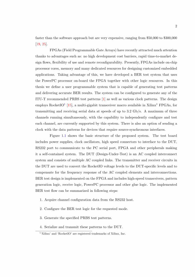
Figure 1.1 shows the basic structure of the proposed system. The test board
includes power supplies, clock oscillators, high speed connectors to interface to the DUT,
RS232 port to communicate to the PC serial port, FPGA and other peripherals making
it a self-contained system. The DUT (Design-Under-Test) is an AC coupled interconnect
system and consists of multiple AC coupled links. The transmitter and receiver circuits in
the DUT are used to convert the RocketIO voltage levels to the DUT-specific levels and to
compensate for the frequency response of the AC coupled elements and interconnections.
BER test design is implemented on the FPGA and includes high-speed transceivers, pattern
generation logic, receive logic, PowerPC processor and other glue logic. The implemented
BER test flow can be summarized in following steps:
1. Acquire channel configuration data from the RS232 host.
2. Configure the BER test logic for the requested mode.
3. Generate the specified PRBS test patterns.
4. Serialize and transmit these patterns to the DUT.1‘Xilinx’ and ‘RocketIO’ are registered trademarks of Xilinx, Inc.

3
Figure 1.1: A high level view of the self-test system
5. Receive the serial bit-stream, deserialize and provide the data to the receive logic.
6. Generate expected data and compare with received data.
7. Calculate the BER statistics based on the above results.
8. Pass the BER data via PowerPC across to the RS232 host.
The PRBS generation, expected data generation, sync logic and serialization/deserialization
modules are developed using Verilog HDL while the code for the PowerPC processor is writ-
ten in C. A unique memory-mapped I/O technique is used to interface the processor and
the verilog modules. This approach greatly reduces the amount of logic resources used
by the bus structures and arbiters in the traditional SoC based designs. The processor is
strictly used for providing user-access and configurability to the high speed BER test logic.
An additional benefit of using a processor-based system is that asynchronous operations,
such as: RS232 interface, configuration subsystem etc. can be performed on the processor
freeing up logic resources for other high-speed modules. All the above mentioned software
functions are coded as subroutines and hence can be used to interface the system to a variety
of customized protocols.

4
1.2 Motivation
The work presented in this thesis is directed by several system-level goals. The
primary goal is to develop an RS232 based self-contained system for a low-earth orbit space
experiment while the secondary goal is to develop a generalized test platform for high-
speed interfaces. The system should be compatible with the Space Plug & Play Avionics
requirements [24] for low-earth orbit satellites and be capable of connecting as a payload to
the satellite bus to perform self-test experiments. Although efforts continue on the layout
of the printed circuit board for the system, the content of this thesis will provide future
workers with design guidelines and experimental results necessary to develop a complete
system.
1.3 Contributions
We make the following contributions in this thesis.
1. The design and implementation of a BER test logic capable of evaluating serial links
with ITU-T recommended test patterns.
2. The development of a self-contained system capable of interfacing with an RS232 host
for user access and configurability.
3. The schematic-level design of a small form factor test vehicle for space experiments
including suggestions for a successful board layout.
4. The demonstration and evaluation of a fully functional system on an FPGA develop-
ment board.
1.4 Thesis Outline
The rest of the thesis is organized as follows. Chapter 2 provides a basic overview of
AC coupled interconnects, Bit Error Rate testing and Space Plug & Play Avionics. Chapter
3 describes the preliminary analysis carried out to select an optimum architecture for the
self-test system. Chapter 4 contains in-depth information about the design of the BER

5
test system. Chapter 5 discusses the implementation of the BER test system on an FPGA
development board. Timing simulations, software testing and performance measurements
are also included. Chapter 6 describes the development of a customized board for the
BERT system. It includes selection of components for optimum working, a rough floorplan
and guidelines for a successful board layout. Chapter 7 concludes this thesis and provides
directions for future work.

6
Chapter 2
Literature Review
2.1 AC Coupled Interconnects
The basic idea of AC coupling stems from the fact that a series capacitor or coupled
inductors placed in the path of a signal will block DC voltage while allowing AC components
to pass. A capacitive connection can be created by bringing into close proximity, two
opposing metal plates on two ICs or on an IC and a substrate [34]. An inductive connection
can be formed likewise, using two spiral inductors. It has been demonstrated by S. Mick et
al. [37, 38] that using such non-contacting structures allow very high density interconnects
to be realized. A complete AC coupled system consists of capacitive or inductive coupling
elements, buried solder bumps for DC connections and transceiver circuits to compensate
for the frequency response of the coupling elements [38].
Figure 2.1: AC coupled interconnect system

7
2.1.1 Capacitive Coupling
A basic circuit schematic for the capacitively coupled structure is shown in Figure
2.2. In this system the series capacitance is formed due to the coupling between the metal
plates built on the corresponding physical structures [34]. This intentional series coupling
capacitance forms a high pass filter while the driver/receiver shunt parasitic capacitances
have a low pass effect, giving the channel an overall bandpass response. A series of inverters
can be used as a transmitter. High pass filtering converts the edges into pulses while low
pass filtering slows the edge rate of the transmitted signal. Finally the signal, arriving in
the form of short pulses, is detected by a pulse receiver [31].
Figure 2.2: Capacitively coupled interconnect structure
SPICE simulations are performed to tune the capacitor value for the required
bandwidth and power. Since the capacitance value also governs the physical dimensions of
the plates and hence the I/O density, tradeoffs are often made to select an optimum value.
Measurements carried out by L. Luo [31] show a 3 Gb/s communication with BER less than
10−12, through a 15 cm channel with 150 fF (75 µm x 75 µm) coupling capacitors in a 0.18
µm design.
2.1.2 Inductive Coupling
A simple schematic of an inductively coupled system is shown in Figure 2.3. Induc-
tors are fabricated on either side of a physical interface and the two surfaces are brought
in close proximity to form a transformer [34]. Inductive coupling has the advantage of
being able to allow larger spacing and hence higher stand-offs than capacitive coupling.
Impedance matching can also be achieved by adjusting the turns ratio. Much like the ca-
pacitively coupled interconnects, the inductively coupled interconnects also has a band pass
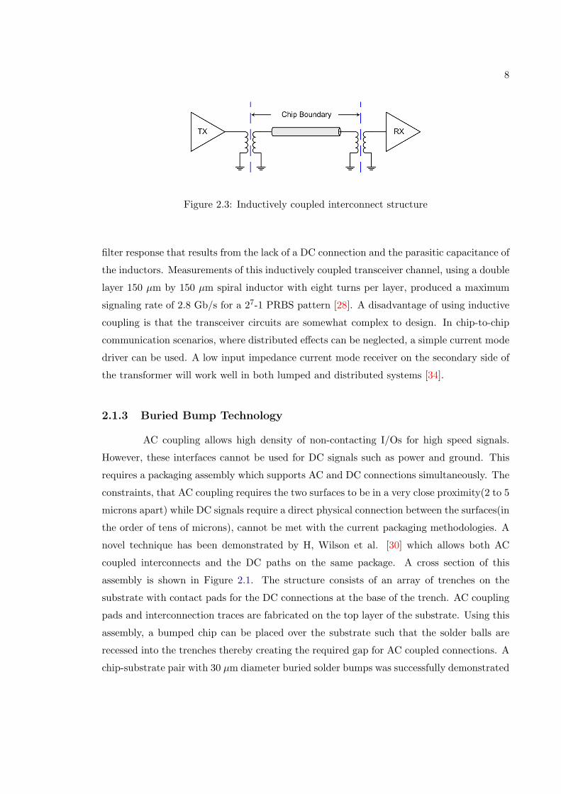
8
Figure 2.3: Inductively coupled interconnect structure
filter response that results from the lack of a DC connection and the parasitic capacitance of
the inductors. Measurements of this inductively coupled transceiver channel, using a double
layer 150 µm by 150 µm spiral inductor with eight turns per layer, produced a maximum
signaling rate of 2.8 Gb/s for a 27-1 PRBS pattern [28]. A disadvantage of using inductive
coupling is that the transceiver circuits are somewhat complex to design. In chip-to-chip
communication scenarios, where distributed effects can be neglected, a simple current mode
driver can be used. A low input impedance current mode receiver on the secondary side of
the transformer will work well in both lumped and distributed systems [34].
2.1.3 Buried Bump Technology
AC coupling allows high density of non-contacting I/Os for high speed signals.
However, these interfaces cannot be used for DC signals such as power and ground. This
requires a packaging assembly which supports AC and DC connections simultaneously. The
constraints, that AC coupling requires the two surfaces to be in a very close proximity(2 to 5
microns apart) while DC signals require a direct physical connection between the surfaces(in
the order of tens of microns), cannot be met with the current packaging methodologies. A
novel technique has been demonstrated by H, Wilson et al. [30] which allows both AC
coupled interconnects and the DC paths on the same package. A cross section of this
assembly is shown in Figure 2.1. The structure consists of an array of trenches on the
substrate with contact pads for the DC connections at the base of the trench. AC coupling
pads and interconnection traces are fabricated on the top layer of the substrate. Using this
assembly, a bumped chip can be placed over the substrate such that the solder balls are
recessed into the trenches thereby creating the required gap for AC coupled connections. A
chip-substrate pair with 30 µm diameter buried solder bumps was successfully demonstrated
9
[30]. In general, AC coupling along with Buried Bump Technology presents a novel physical
structure that allows both DC connections and AC coupled paths (capacitive or inductive)
across the same interface while maintaining low power, high density, and high data rate
communication between integrated circuits.
2.2 Bit Error Rate Testing
BER (Bit Error Rate) is technically defined as the number of erroneous bits divided
by the total number of bits transmitted, received, or processed over some stipulated period
[6]. It is just one of many statistical measures of a communication link or channel, and is
usually expressed as a negative power of ten.
Bit Error Rate =Bit errors
Total number of bits
For example, if the BER is 10−9, we expect that there will be one bit in error, on
average, for every 1 billion bits received. A bit error occurs when a system fails to identify
the correct logic level of the received bit. The process of BER measurement is simple -
transmit a known data stream through the system-under-test and compare the received
data with the expected data. Since BER depends on probability, this number represents
the actual BER of the link only if the number of transmitted bits approaches infinity. A
more practical approach is to use sufficiently long PRBS patterns, that simulate actual
traffic. The ITU-T (International Telecommunication Union-Telecommunications sector)
provides special recommendations [1] to generate industry-standard data patterns used for
BER testing. The results are generally evaluated based on confidence level which increases
with longer run times. The confidence level is defined as the probability, based on a set of
measurements, that the actual probability of an event is better than a specified level [3].
A key component of any BER measurement system is the SerDes (Serializer /
Deserializer) device. The serializer block accepts parallel data and converts it to a high-
speed single-bit serial output. The deserializer block contains a clock and data recovery unit
that extracts the clock from the serial data and adjusts the serial data with respect to the
extracted clock. The data is then demultiplexed to provide a parallel output. An important
requirement for the use of such devices in BER testing is that the intrinsic BER should be
zero. In other words, when the serializer output is directly connected to the deserializer

10
input, there should be no erroneous data reception. Some of the major factors that affect
BER include signal-to-noise ratio, jitter, EMI, crosstalk, and poor extinction ratio [2].
Figure 2.4: A basic BER measurement system (a) Loopback (b) End-to-end
A typical BER testing system consists of a pattern generator, an electrical or
optical transmitter and receiver, the error detector and the system-under-test. Two types
of configurations are generally used, as shown in Figure 2.4(a) where the pattern generator
and the error detector reside at the same location, and Figure 2.4(b) where the pattern
generator and error detector reside at different locations, possibly miles apart. The latter
is generally used for the characterization of under-the-sea optical links or long network
cables, while the former is used in design lab or production testing area since both pattern
generation and detection can be done on a single system. In both cases specific PRBS
patterns, based on the above standards, are used to calculate the BER.
With today’s systems having low error probability, a large number of bits are
needed to achieve a meaningful estimate of the system performance, which makes it a tedious
and time consuming process. Several methods like artificial channel degradation [35], AC
stimulus [26], SNR-based measurements and the most popular, Q-factor measurements are
proposed to accelerate the process of BER measurement. Each of these methods reduce
BER measurement time by either sacrificing a little bit of accuracy, by assuming a gaussian
distribution for the errors or by extrapolating the BER values under artificially induced
noise.

11
2.3 Space Plug & Play Avionics
A new paradigm ORS (Operationally Responsive Space), introduced by the De-
partment of Defense, is widely being researched in the aerospace industry. This concept
is concerned with a dramatic reduction in time to field a solution for space vehicles [12].
Currently, space equipment requires years to develop due to their complex design, stringent
requirements, testing and manufacturing processes. This existing capability is not oper-
ationally responsive. Instead of waiting months to carry out a launch, ORS envisions a
small launch vehicle that could be ready for launch in weeks, if not days, after start. Rapid
development of a space vehicle is presented with a number of technical challenges, even
when extensive standardization is enforced.
A unique system to reduce the design time for the space vehicles, based on the
conventional PnP (Plug-and-Play) approach, is being developed by AFRL (Air Force Re-
search Laboratory) [29]. This SPA (Space Plug-and-play Avionics) system is based on the
standards intended to promote the rapid development of spacecraft busses and payloads.
It combines the commercial standards (such as USB, RS232) with the specific hardware
components and software necessary to build a real-time embedded system. SPA is based on
the existing USB (version 1.1) interface, which supports 12Mb/s data transport, suitable
for interfacing with most spacecraft devices. This design approach allows the use of existing
USB intellectual property for implementing rad-hard designs, while providing the additional
support needed for power and synchronization of spacecraft components.
2.3.1 Applique Sensor Interface Module
The ASIM (Applique Sensor Interface Module) is a combination of hardware,
firmware and a defined set of commands [24]. An ASIM functions as a bridge between a
typical SPA interface and a user module and delivers automatic support for useful services
including power management, synchronization, electronic data sheet etc. The user module
refers to any experimental system, or a pre-developed payload. The ASIM performs the
conversion of data format from the SPA host to a data format supported by the user module
and vice versa. Thus an ASIM provides a means for the host computer to request data from
the user module, test its functionality and issue commands to effect the operation of the
module. The command language consists of several ASCII codes that provide communica-
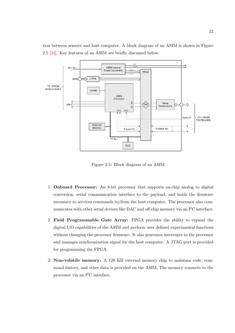
12
tion between sensors and host computer. A block diagram of an ASIM is shown in Figure
2.5 [24]. Key features of an ASIM are briefly discussed below:
Figure 2.5: Block diagram of an ASIM
1. Onboard Processor: An 8-bit processor that supports on-chip analog to digital
conversion, serial communication interface to the payload, and holds the firmware
necessary to services commands to/from the host computer. The processor also com-
municates with other serial devices like DAC and off-chip memory via an I2C interface.
2. Field Programmable Gate Array: FPGA provides the ability to expand the
digital I/O capabilities of the ASIM and perform user defined experimental functions
without changing the processor firmware. It also generates interrupts to the processor
and manages synchronization signal for the host computer. A JTAG port is provided
for programming the FPGA.
3. Non-volatile memory: A 128 KB external memory chip to maintain code, com-
mand history, and other data is provided on the ASIM. The memory connects to the
processor via an I2C interface.

13
4. User facilities: User features include digital I/Os, analog I/Os, and serial ports.
The provision of such features in the ASIM promotes close-coupling of user designs
to the SPA interface, simplifies coding and reduces physical overhead.
5. Power management: An ASIM receives 28 V DC from a spacecraft bus. The
onboard voltage regulator provides the necessary voltages at no less than 500 mA ±1%. Device power is managed through switchable relay connections controlled by the
processor.
6. Clock management: Two crystal oscillators provide a 100 MHz oscillator that
drives the logic on the FPGA and a 32.768 KHz oscillator that is connected to the
processor. The ASIM also manages the synchronization pulse from the SPA interface
and makes timestamps available.
14
Chapter 3
Groundwork and Initial Analysis
The primary objective of this thesis is to design an automated BER test system
capable of providing user-access and configurability through an RS232 interface. The in-
tention is to develop a stand-alone vehicle that can interface with the SPA [24] electronics
of the satellite while maintaining a versatile architecture that can be reused for other appli-
cations. With the requirement not specific towards a particular implementation, there are
multiple ways in which this system can be designed. Two architectures that closely match
the target application are described with their advantages and disadvantages discussed.
3.1 Microcontroller based system
Microcontrollers offer an efficient and robust alternative for designing data process-
ing systems. On-chip resources of a microcontroller may include a high-speed processor,
flash memory, UART, bus interfaces, timers and counters [13]. Analog features such as:
ADC, voltage reference, internal oscillator, comparators and temperature sensor are also
often integrated. Because the programming is done with software, detailed simulations may
be performed in advance to assure correctness of functionality. The use of flash memory to
store the program allows for flexibility of multiple configurations. In the past, programming
a microcontroller often involved tedious assembly coding. However, C-based compilers are
available now for most microcontrollers, which greatly reduces design time.
15
3.1.1 Serializer/Deserializer Module
The ‘SCAN50C400A’ is a four channel high-speed transceiver (SerDes) module
from National Semiconductor [16], capable of supporting data rates of up to 1.25 Gb/s per
channel. The on-chip BIST (Built-In Self Test) logic is capable of generating and testing four
different PRBS patterns (27-1, 213-1, 223-1 and 231-1). An error detector is also included to
compare recovered data with the expected data generated by the on-chip BIST logic. An
8-bit counter stores the number of errors detected in the received bit stream. Internal low
jitter PLLs are used to derive the clock from the received high-speed serial data stream.
Initially, a synchronization data header is transmitted to establish byte boundaries at the
receiver. The selection of PRBS pattern, access of the error counter and other configuration
registers are carried out via the SPI (Serial Peripheral Interface). Multiple registers are used
for storing the control and status information.
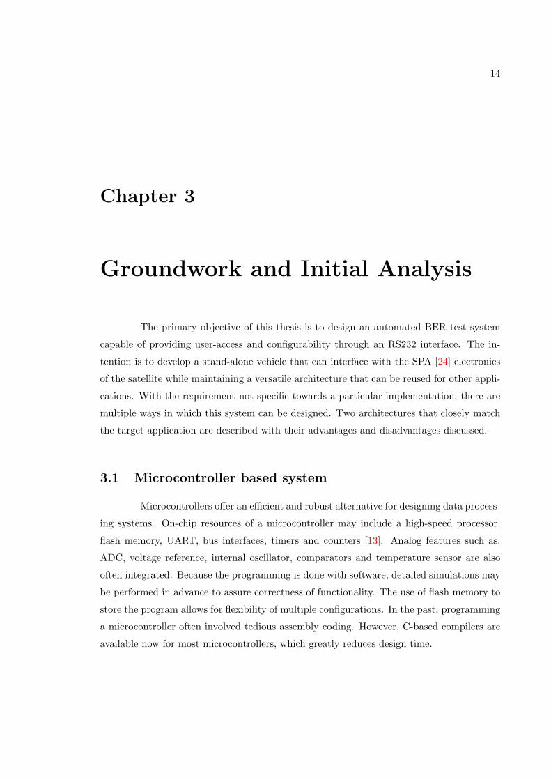
3.1.2 Proposed Design
Figure 3.1: Microcontroller based self-test system
Figure 3.1 shows a conceptual block diagram of a microcontroller based self-test
system that employs the previously discussed transceiver. The transceiver is connected
to the microcontroller by an SPI bus for control and configuration. For simplicity’s sake,
voltage regulator, clock oscillator, and other components are not shown. The high-speed
connector can be attached to a DUT or to a loopback interface. The operation of this
system can be summarized in the following steps:

16
1. The microcontroller selects and customizes the test patterns through the SPI.
2. The test is run for a specific period of time.
3. The microcontroller reads the error register value.
4. The results are sent out the results through the RS232 interface.
The microcontroller performs the BER measurment using the error values received
from the transceiver. An interactive user-interface can be setup to allow configuration of the
PRBS patterns and gathering of the status information through the RS232 connection. The
code for the microcontroller can be written in C. A standard C2 interface can be provided
for in-system programmability of the microcontroller.
3.2 FPGA based system
As discussed earlier, FPGAs provide a convenient and inexpensive approach to
designing digital logic. FPGAs share certain advantages with microcontrollers such as ease
of design, infinite reconfigurations, support for standard interfaces, on-chip microprocessor
etc. In addition to these, newer FPGAs have on-chip multi-gigabit serial transceivers. For
the application under consideration, this feature allows the entire system to be built on a
single FPGA.
3.2.1 RocketIO Transceiver
RocketIO is a multi-gigabit programmable transceiver module embedded in the
FPGA fabric. Xilinx FPGAs can have up to 20 RocketIO transceivers on-chip, with each
transceiver allowing data rates from 600 Mb/s to 3.125 Gb/s [15]. A monolithic clock
synthesis and clock recovery system eliminates the need for external components. The
output voltage level is user-programmable with differential swings from 800 mV to 1600 mV
peak-to-peak to provide compatibility with other serial voltage standards. Other features
include on-chip termination, internal loopback modes for testing, and programmable pre-
emphasis. A simple block diagram of a RocketIO transceiver is shown in Figure 3.2.
Multiple RocketIO transceivers can be synchronized to form higher bandwidth
data links. For example, a XAUI interface can be designed by bonding four serial channels,

17
Figure 3.2: RocketIO tranceiver module (Courtesy: Xilinx Inc.)
each running at 2.5 Gb/s, to form a single 10 Gb/s link. The RocketIO transceiver’s
programmable features allow the transceiver to be easily integrated with the digital logic
on the FPGA.
3.2.2 Proposed Design
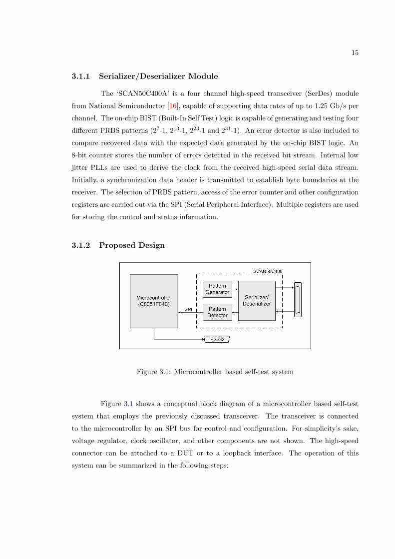
An FPGA based self-test system is shown in Figure 3.3. The idea is to develop
logic for generating parallel PRBS patterns, error detection and BER calculations using
Verilog or VHDL. RocketIO transceivers can be used to serialize/deserialize the data. HDL
wrappers can be used to integrate the RocketIOs with the PRBS generation and error
detection modules. The PowerPC processor on the FPGA can be used to communicate
over the required RS232 interface for configuration and error reporting. EDK (Embedded
Design Kit) provided by Xilinx Inc. is used to develop code for the processor and logic to
interface the processor with the digital logic.
At the architectural level, we find the FPGA based approach more feasible and
advantageous. The following lists the chief reasons behind our selection of the FPGA based
system over the microcontroller based system:
1. The entire system can be developed on a single FPGA unlike the microcontroller
18
Figure 3.3: FPGA based self-test system
based system which requires multiple discrete components.
2. Reduced number of components means fewer PCB traces and hence a simpler design.
3. More application-specific features can be provided on the FPGA as compared to the
commercial SerDes part which has limited functionality.
4. The system can be easily ported to next generation FPGAs for future applications.
5. The design can be modified and extended to serve a multitude of systems.
6. Other drawbacks of microcontrollers include limited I/Os, limited amount of on-chip
memory and lower speed of operation.
The only concern with the FPGA based system is the power consumption. The
FPGAs use look-up tables, which are not power-efficient, for logic implementation. Hence,
they tend to consume more power than the conventional microcontrollers. Since this system
will be used as a part of avionics and has restrictions for the maximum power consumption,
we perform a pre-implementation power analysis (discussed in the next section) to estimate
the power consumption.
19
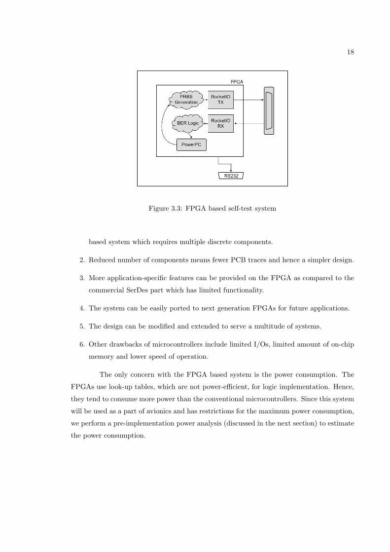
3.2.3 Eye Diagrams
To finalize the selection process of the architecture, we performed a transmitter
characterization of the RocketIOs. This includes the observation of the output waveform,
voltage swings and jitter values for the serial transmitters. Figure 3.4 shows the transmitter
output when the parallel input is a sequence of interleaved zeros and ones, which produces
a clock signal. The serial data rate is 3.2 Gb/s (1.6 Ghz) and no pre-emphasis is used.
The output voltage swing is 1600 mV (p-p) with a common-mode voltage of 1.7 V. The
peak-to-peak jitter is 20 ps.
Figure 3.4: Eye diagram of RocketIO TX with clock pattern
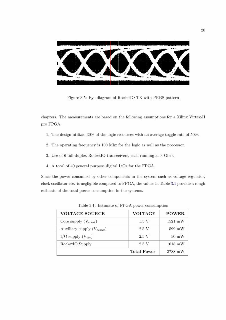
Figure 3.5 shows the transmitter output when the parallel input is a PRBS pattern
from an LFSR for a serial data rate of 3.2 Gb/s. The output voltage swing is 1600 mV
(p-p) and no pre-emphasis is used. The peak-to-peak jitter is 50 ps.
3.3 Power Analysis
Since power consumption is one of the important criteria in designing payloads for
space experiments, we perform a pre-implementation power analysis of the FPGA based
system. Xilinx Inc. provides unique Power Tools that estimate the power consumption of
an FPGA based on the expected utilization of device resources, operating frequencies, and
average toggle rates. The actual values will be measured and discussed in the following
20
Figure 3.5: Eye diagram of RocketIO TX with PRBS pattern
chapters. The measurements are based on the following assumptions for a Xilinx Virtex-II
pro FPGA.
1. The design utilizes 30% of the logic resources with an average toggle rate of 50%.
2. The operating frequency is 100 Mhz for the logic as well as the processor.
3. Use of 6 full-duplex RocketIO transceivers, each running at 3 Gb/s.
4. A total of 40 general purpose digital I/Os for the FPGA.
Since the power consumed by other components in the system such as voltage regulator,
clock oscillator etc. is negligible compared to FPGA, the values in Table 3.1 provide a rough
estimate of the total power consumption in the systems.
Table 3.1: Estimate of FPGA power consumption
VOLTAGE SOURCE VOLTAGE POWER
Core supply (Vccint) 1.5 V 1521 mW
Auxiliary supply (Vccaux) 2.5 V 599 mW
I/O supply (Vcco) 2.5 V 50 mW
RocketIO Supply 2.5 V 1618 mW
Total Power 3788 mW
21
Chapter 4
BER Test System Design
4.1 Hardware Design
This section describes the logic design of a multi-channel BERT (Bit Error Rate
Test) module. This module generates and tests non-encoded serial data on one or more
channels (150 Mb/s to 3.125 Gb/s) between the RocketIO transceivers in the FPGA. The
serial data to be transmitted is constructed in the FPGA fabric using LFSR-based pat-
tern generators together with the RocketIO transceivers. The receiver module consists of
self-synchronizing logic to generate the expected data and analyze the incoming data for
errors. Each channel has the ability to load a different data pattern and perform the BER
measurements independently of other channels.
4.1.1 PRBS Pattern Generation
PRBS (Pseudo-Random Bit Sequence) is a pattern which appears to be random,
but is actually a reproducible and repeatable sequence having sufficiently long periodicity.
PRBS patterns are logically generated bit sequences that exhibit statistical characteristics
similar to a truly random sequence and simulate real traffic. Reproducible patterns are
a prerequisite to perform end-to-end measurements. PRBS patterns with lengths of 2n-1
(‘n’ denotes number of stages in the LFSR) bits are the most common solutions for such
applications.
22
Linear Feedback Shift Register
PRBS patterns are usually produced using an LFSR (Linear Feedback Shift regis-
ter). An n-stage LFSR, with appropriate feedback, can produce a sequence with a maximum
length of 2n-1 bits. The hardware consists of an n-stage shift register with the contents of
the registers shifted right by one position every clock cycle. The outputs from predefined
registers are XORed together and fed back to the leftmost register. The longest string of
consecutive zeros in a n-stage LFSR is equal to (n-1) [4]. There are two types of LFSR
implementations, for any polynomial, that produce equivalent output:
1. Fibonacci LFSR- which uses XOR gates outside the shift register chain.
2. Galois LFSR- which uses XOR gates inside the shift register chain.
An implementation of a multi-stage LFSR can be represented mathematically in the form
of a polynomial. For example, x9 + x5 + 1 indicates a Fibonacci LFSR implementation of
a 9-stage shift register, with the outputs from 5th and 9th stage XORed and fed back to
the input. Fibonacci implementation generally achieves faster clock speeds than the Galois
implementation, for LFSRs with fewer taps [5]. PRBS generators used in our design employ
Fibonacci implementation.
Figure 4.1 shows the block diagram of our LFSR-based PRBS generator. The
PRBS generator is fully parameterizable and can be configured to output a variety of PRBS
patterns. The configurable parameters for this module are:
1. N: Width of the parallel data output.
2. LENGTH: Length of the PRBS pattern.
3. INVERT: Inversion of the data prior to the output.
4. POLY: The LFSR polynomial in binary with each bit indicating the feedback tap.
The use of parameterizable modules helps to reduce design time by increasing the reusability
of the module in different configurations. Let us take an example of designing a 29-1
PRBS pattern generator with a 20-bit non-inverted output. The polynomial to generate a
maximum length sequence for a 9-stage LFSR is x9+x5+1. Hence the parameter values for
the above configuration are: N = 20, LENGTH = 9, INVERT = 0, and POLY = 100010000
(indicating that the output from the 5th and 9th registers should be XORed). When the
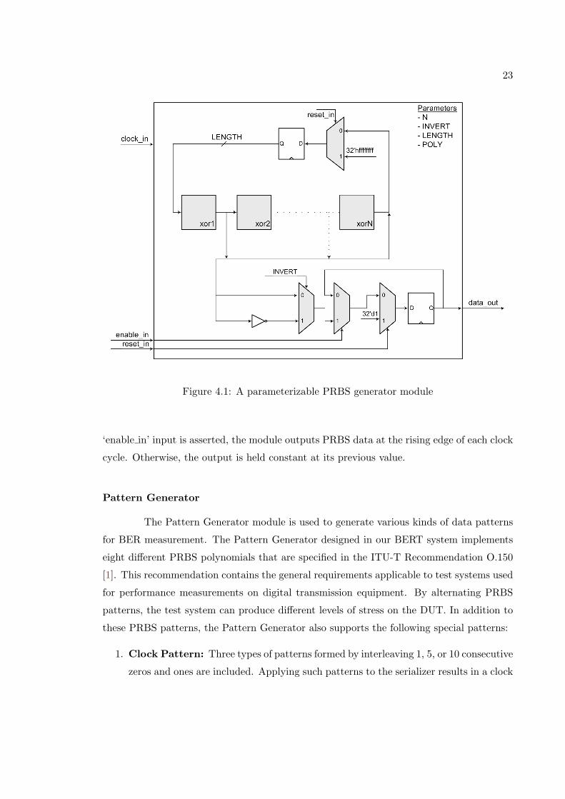
23
Figure 4.1: A parameterizable PRBS generator module
‘enable in’ input is asserted, the module outputs PRBS data at the rising edge of each clock
cycle. Otherwise, the output is held constant at its previous value.
Pattern Generator
The Pattern Generator module is used to generate various kinds of data patterns
for BER measurement. The Pattern Generator designed in our BERT system implements
eight different PRBS polynomials that are specified in the ITU-T Recommendation O.150
[1]. This recommendation contains the general requirements applicable to test systems used
for performance measurements on digital transmission equipment. By alternating PRBS
patterns, the test system can produce different levels of stress on the DUT. In addition to
these PRBS patterns, the Pattern Generator also supports the following special patterns:
1. Clock Pattern: Three types of patterns formed by interleaving 1, 5, or 10 consecutive
zeros and ones are included. Applying such patterns to the serializer results in a clock

24
output with the frequency equal to 1/2, 1/10th, or 1/20th of the serial data rate.
2. User Pattern: This pattern consists of any 20-bit word that is specified by the user
during implementation phase.
3. Counter Pattern: This pattern consists of 20-bit incremental counter values, pro-
viding a traceable and predictable pattern, as opposed to the PRBS pattern. This
feature also allows to test for the latency between the transmit and the receive logic
and eases the debugging process.
Figure 4.2: Pattern Generator module
Figure 4.2 shows the block diagram of our Pattern Generator module. It contains
16 individual pattern generating blocks and generates 20-bit patterns to ease the interfacing
with the 20-bit transceiver input. Among the eight PRBS patterns implemented, four of
them use inverted outputs. ITU-T considers the inverted patterns to be more stressful than
the non-inverted patterns for testing the clock recovery circuit.
The PRBS generators are implemented using various parameterized instantiations
of the PRBS module, that was discussed earlier. The outputs of all these blocks are mul-
tiplexed, with the selection lines driven by a 4-bit ‘patten select’ input. Thus, depending
upon the value of this signal a particular block is selected. The output of the multiplexer is

25
Table 4.1: Supported patterns in the BERT design
ID Pattern and Length Zeros RemarksPolynomial (Bits)
0 1/2 Clock 2 0 This pattern can be used to generate a(101010) clock signal with the frequency equal to
1/2 the transceiver serial rate.
1 1/10 Clock 10 5 This pattern can be used to generate a(5 ones 5 zeros) clock signal with the frequency equal to
1/10th the transceiver serial rate.
2 1/20 Clock 20 10 This pattern can be used to generate a(10 ones 10 zeros) clock signal with the frequency equal to
1/20th the transceiver serial rate.
3 PRBS (x7 + x6 + 1) 27-1 6 N/A
4 PRBS (x9 + x5 + 1) 29-1 8 ITU-T Recommendation O.150 (5.1)
5 PRBS (x11 + x9 + 1) 211-1 10 ITU-T Recommendation O.150 (5.2)
6 PRBS (x15 + x14 + 1) 215-1 15 ITU-T Recommendation O.150 (5.3)
7 PRBS (x20 + x3 + 1) 220-1 19 ITU-T Recommendation O.150 (5.4)
8 PRBS (x20 + x17 + 1) 220-1 14 ITU-T Recommendation O.150 (5.5)This sequence outputs a one for everyinstance of 14 consecutive zeros.
9 PRBS (x23 + x18 + 1) 223-1 23 ITU-T Recommendation O.150 (5.6)
10 PRBS (x29 + x27 + 1) 229-1 29 ITU-T Recommendation O.150 (5.7)
11 PRBS (x31 + x28 + 1) 231-1 31 ITU-T Recommendation O.150 (5.8)
12 PRBS (x32 + x31 +x30 + x10 + 1)
232-1 31 N/A
13 User Pattern 20 N/A Any 20-bit sequence
14 1/4 Clock 4 2 This pattern can be used to generate a(11001100) clock signal with the frequency equal to
1/4th the transceiver serial rate.
15 Counter Pattern 220 20 20-bit counter sequence
registered before being provided at the 20-bit output port. The Pattern Generator module
has the ability to artificially inject errors into the output data using the ‘error inject’ input.

26
When this input is asserted, all the bits at the output are inverted to introduce a burst of
bit-errors in the serial transmission. This feature helps to check the integrity of the BER
logic on the receive side. Table 4.1 lists all the patterns supported by this module together
with their polynomials, sequence lengths and maximum number of consecutive zeros. The
option to implement a particular pattern generating block, is controlled by a set of values
in the configuration file during implementation phase. This feature helps to easily remove
or add PRBS blocks for a smaller design or reduced functionality.
Transmitter
Figure 4.3: Transmitter module
The idea for the transmit logic is to provide the parallel data from the pattern
generators to the RocketIOs. This data is then serialized by the RocketIOs and sent out
to the DUT. Similarly, a serial data stream is received from the DUT and is deserialized
by the RocketIOs to provide parallel data, which is then analyzed by the receive logic.
The fundamental problem in this approach is the inability of the RocketIOs to determine
byte boundaries in the received random serial data. To handle this situation, special pre-
defined bit sequence called ‘Comma’ is transmitted initially. Comma is a 20-bit word that
is defined by the user at the time of implementation. A part of logic on the receive side
constantly searches for the Comma words in the received data. When a match is found,
the receiver generates necessary control signals to establish the byte boundaries. With the
27
byte boundaries defined, the receiver is then ready to accept random data.
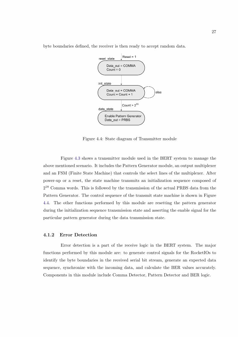
Figure 4.4: State diagram of Transmitter module
Figure 4.3 shows a transmitter module used in the BERT system to manage the
above mentioned scenario. It includes the Pattern Generator module, an output multiplexer
and an FSM (Finite State Machine) that controls the select lines of the multiplexer. After
power-up or a reset, the state machine transmits an initialization sequence composed of
218 Comma words. This is followed by the transmission of the actual PRBS data from the
Pattern Generator. The control sequence of the transmit state machine is shown in Figure
4.4. The other functions performed by this module are resetting the pattern generator
during the initialization sequence transmission state and asserting the enable signal for the
particular pattern generator during the data transmission state.
4.1.2 Error Detection
Error detection is a part of the receive logic in the BERT system. The major
functions performed by this module are: to generate control signals for the RocketIOs to
identify the byte boundaries in the received serial bit stream, generate an expected data
sequence, synchronize with the incoming data, and calculate the BER values accurately.
Components in this module include Comma Detector, Pattern Detector and BER logic.
28
Comma Detector
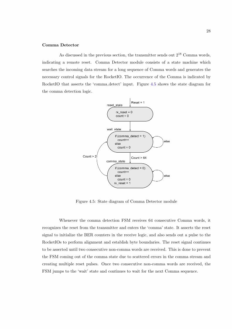
As discussed in the previous section, the transmitter sends out 218 Comma words,
indicating a remote reset. Comma Detector module consists of a state machine which
searches the incoming data stream for a long sequence of Comma words and generates the
necessary control signals for the RocketIO. The occurrence of the Comma is indicated by
RocketIO that asserts the ‘comma detect’ input. Figure 4.5 shows the state diagram for
the comma detection logic.
Figure 4.5: State diagram of Comma Detector module
Whenever the comma detection FSM receives 64 consecutive Comma words, it
recognizes the reset from the transmitter and enters the ‘comma’ state. It asserts the reset
signal to initialize the BER counters in the receive logic, and also sends out a pulse to the
RocketIOs to perform alignment and establish byte boundaries. The reset signal continues
to be asserted until two consecutive non-comma words are received. This is done to prevent
the FSM coming out of the comma state due to scattered errors in the comma stream and
creating multiple reset pulses. Once two consecutive non-comma words are received, the
FSM jumps to the ‘wait’ state and continues to wait for the next Comma sequence.

29
Pattern Detector
Figure 4.6: Pattern detector block diagram
The Pattern Detector module provides many functions. It receives the parallel
data from the RocketIOs, generates and synchronizes the expected data, and determines
the number of bit errors in an erroneous frame. It is a core component of the BERT system.
The block diagram of the Pattern Detector module is shown in Figure 4.6.
Since the Pattern Detector has to generate the expected data values to compare
with the incoming data, it contains another instance of the Pattern Generator module,
same as the one on the transmit side. When the reset is asserted, either during power-up or
by the Comma Detector when it receives the initialization sequence, the Pattern Detector
initializes the counters and freezes the expected data at the Pattern Generator output.
This initial data is compared against a delayed value of the incoming data stream. The
delay (flip-flop) element is used to ensure that the Pattern Generator has enough time to
get enabled and generate the next value without dropping any incoming frames, when a
match is found. This process continues until the expected data matches the incoming data.
Thus, the Pattern Detector automatically aligns to the incoming data stream. This entire
operation is managed by the Pattern Detection FSM. The control sequence of the FSM is
shown in Figure 4.7.
After a reset, as the FSM logic monitors the incoming data for a match, a ‘wait’
signal is asserted at the output indicating that the system is waiting for a valid data stream.
Once aligned, the pattern generator is enabled to produce the subsequent values. To avoid

30
Figure 4.7: Pattern detector state diagram
false triggering by a random match, the system enters the ‘lock’ state only after two con-
secutive matches are found. The ‘lock’ state indicates that the FSM has successfully syn-
chronized with the incoming data pattern and is ready for BER measurements. If any error
is found after the link is established, it calculates the bit errors in that frame and raises
an error flag. The ‘lock’ signal remains asserted until the module detects three consecutive
frames in error. At this point, the system enters the ‘abort’ state indicating that the system
is not stable for BER measurements. This is done to avoid a burst of errors being taken
into account for BER measurement. The system continues to remain in the ‘abort’ state
until a reset is received.
Receiver
This module maintains counters for the total number of frames received, total
number of error frames and total bit errors. The width of the counters is parameterizable
during implementation using the configuration file. It contains the Comma Detector and

31
Pattern Detector modules. The block diagram of this module is shown in Figure 4.8.
Figure 4.8: Receiver Module
In the event of a system reset or the assertion of ‘rx reset’ signal by the Comma
Detector module, all the BER counters are reset. The receiver module also outputs a
‘enable comma align’ signal, to the RocketIOs to enable alignment of the byte boundaries.
The module waits until the pattern detector has successfully aligned to the incoming data
stream. After that, until the link remains established, the ‘total frames’ counter is updated
every cycle to keep track of the total received frames. The ‘error frames’ counter is updated
every time the pattern detector asserts the error flag. The ‘bit errors’ counter aggregates
the number of erroneous bits of all the frames received in error. This number is essential
for calculating the BER. The receiver module outputs an ‘overflow’ signal if the bit error
counter overflows. A special counter which calculates the error interval is also included.
This value indicates the number of frames between the last two occurrences of an error.
This may prove to be important parameter while analyzing the BER performance of the
channel.
4.1.3 RocketIO Transceiver
As mentioned earlier, RocketIOs are SerDes devices used to convert the parallel
PRBS data from the transmitter to high speed serial data and vice versa. RocketIOs are
employed in the design by instantiating the HDL wrappers. By mapping digital port con-
32
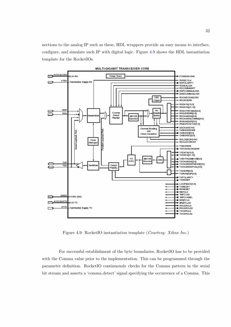
nections to the analog IP such as these, HDL wrappers provide an easy means to interface,
configure, and simulate such IP with digital logic. Figure 4.9 shows the HDL instantiation
template for the RocketIOs.
Figure 4.9: RocketIO instantiation template (Courtesy: Xilinx Inc.)
For successful establishment of the byte boundaries, RocketIO has to be provided
with the Comma value prior to the implementation. This can be programmed through the
parameter definition. RocketIO continuously checks for the Comma pattern in the serial
bit stream and asserts a ‘comma detect’ signal specifying the occurrence of a Comma. This

33
signal is used by the Comma Detector to determine a remote reset from the transmitter.
If a valid reset is determined then the receiver outputs a ‘enable comma align’ signal to
the RocketIO. The transceiver then checks the current alignment and performs realignment
of the boundaries, if needed. RocketIO also houses a clock recovery circuit that extracts
the clock from the received serial data. The parallel data after deserialization and the
‘comma detect’ signal are synchronous with this recovered clock. Considering this and the
need to reduce the load on the transmit clock, the receive logic is clocked with respect to
the recovered clock.
The RocketIO transceiver module contains 50 ports. The high-speed serial data
ports (RXN, RXP, TXN, and TXP) are connected directly to the external pads while the
remaining 46 ports are accessible to the digital logic on the FPGA.
4.1.4 Single-channel BERT Module
The single-channel BERT is a self-contained BER test module that can be im-
plemented on the FPGA, independent of the PowerPC subsystem. It can be replicated in
the FPGA fabric to create multiple stand-alone BERT channels. A single-channel BERT
contains three primary modules: Transmitter, RocketIO, and Receiver. In order to perform
a successful BER measurement, the PRBS pattern sent out by the transmitter must match
the pattern expected at the receiver. To achieve this, the ‘pattern select’ input is connected
to both, the Transmitter as well as the Receiver modules. Figure 4.10 shows the block
diagram of the single-channel BERT module. The operation of the single-channel BERT
can be summarized as followed:
1. After power-up, the Transmitter module sends an initialization sequence consisting of
Comma words, that are pre-programmed by the user, followed by the actual PRBS
data.
2. The RocketIO takes in the parallel data and sends out serialized data. This data can
be either passed through an external DUT or can be looped back using the RocketIO’s
loopback mode to the serial inputs.
3. During this time, the Receiver module locks the Pattern Generator output at its first
data. The PRBS patterns are selected by the ‘pattern enable’ signal, on the transmit
as well as the receive side.

34
Figure 4.10: Single-channel BERT module
4. The RocketIO extracts the clock from the serial data, and provides it to the Receiver
module along with the parallel data. It also asserts the ‘comma detect’ signal if it
receives a Comma sequence.
5. The ‘Receiver’ module acknowledges a remote reset by asserting the ‘enable comma align’
for the RocketIOs to establish byte boundaries.
6. Once the PRBS data starts arriving, the Receiver synchronizes itself with the incoming
data and starts performing BER measurements.
7. The BER data is then passed through an asynchronous FIFO to synchronize the data
with the external clock and is presented at the output.
An edge detect logic block is developed for the ‘error insert’ input, that sends
a pulse of exactly one cycle duration to the Transmitter module, everytime the input is
toggled. This ensures the creation of a single error frame in the transmitted data stream,
rather than a burst of errors whenever the ‘error insert’ signal is asserted for more than
one cycle. As specified earlier, the Receiver module is clocked using the recovered clock
from the received bit stream. Thus, the BER data calculated by the receive logic will be

35
synchronous with respect to that clock. This approach is only feasible if the BERT system is
implemented on the FPGA as a stand-alone module. If multiple channels are implemented,
the BER data of each channel will be synchronous with their respective recovered clock.
Even though the frequencies of all the recovered clocks match, their phases are different
and may result in metastable conditions if a top-level control module is used to gather the
BER statistics of the channels. Hence there is a need to synchronize the BER data of all
channels with a common external clock.
Successfully crossing clock domain requires proper handshaking. This approach
also requires development of control logic which consumes the resources on the FPGA.
An alternative is to use asynchronous FIFOs i.e. FIFOs with different read and write
clocks. The write side uses a continuously running write clock while the read side uses a
continuously running read clock. FIFOs can be easily implemented by using the block RAMs
on the FPGA, thus saving logic resources. A dual-port block RAM will allow independent
operation of each port. We have developed an 8-location deep FIFO for our BERT module
using the block RAM on the FPGA. The write side is clocked using the recovered clock
while the read side is clocked with respect to a transmit clock. This approach ensures stable
and efficient transfer of BER data across clock domains.
Single-channel BERT module supports two different reference clocks for the trans-
ceiver. These reference clocks drive the PLLs used to generate high speed clocks for the
internal circuitry and determine the serial data rate. Either of the reference clocks can be
selected by the ‘refclk sel’ input. This allows flexibility of changing the serial data rate
dynamically during run-time by toggling the clock select input. The transmit clock, as dis-
cussed in the later sections, is derived from the reference clocks. So, if the reference clocks
are toggled for changing the serial rate, the transmit clock must be appropriately derived
from the selected reference clock. Whenever the reference clock changes, the ‘mgt reset’ pin
must be asserted for at least 3 cycles for the PLLs to synchronize with the new clock.
4.1.5 Multi-channel BERT Module
The multi-channel BERT module is developed by instantiating three single-channel
BERT modules. It also includes the address mapping logic used to allow access to the
internal registers of the BERT modules, using a GPIO interface. The maximum number
of BERT channels that can be implemented depends upon the type of FPGA to which

36
the system is mapped. Figure 4.11 shows the block diagram of the multi-channel BERT
module.
Figure 4.11: Multi-channel BERT module
The RocketIO transceivers are embedded on the top and bottom edges of the
actual FPGA. To ensure less skew on the clock lines and hence produce a clean output, it
is recommended to use separate reference clocks for the RocketIOs located on the top and
bottom banks of the FPGA. In order to allow the flexibility to use transceivers located on
either of the banks for the BERT channels, we provide separate clock and reset inputs for
the top and bottom banks. The location of the transceivers used for the BERT channels
37
can be programmed during the implementation phase. Depending upon the location (top
or bottom edge of the FPGA) of the transceiver the corresponding BERT channel must be
driven by the clock for that particular bank. The user accessible ports on the multi-channel
BERT module are defined in Table 4.2.
Besides including the single-channel BERT modules, the multi-channel BERT also
contains serial clock generation logic. This feature is useful when a synchronous clock
is needed together with the data for source-synchronous interfaces. As discussed in the
pattern generation section, the RocketIO transceivers can be made to transmit a clock by
providing a pattern consisting of interleaved zeros and ones. The input for the RocketIOs
employed for the clock generation is hardwired to the clock pattern (101010). Use of this
configuration will result in a clock signal with a frequency that is 1/2 the serial data rate.
For a source-synchronous interface, we need a clock signal that has the same frequency as
the synchronous bit rate. This can be achieved by either doubling the reference clock of
the RocketIOs used for clock generation or halving the reference clock of the RocketIOs
that generate the PRBS data. The former approach is not feasible since it would involve
the clock generation transceiver to work at 6 Gb/s which is not currently supported for
the RocketIOs. Hence the latter approach is utilized in our BERT system. The FPGA
specifications require that all the transceivers on a particular bank (top or bottom) must be
clocked by the same reference clock. Therefore the data and clock modules are implemented
on the opposite banks, with the data generation modules using the reference clock that is
1/2 the frequency of the clock generation modules. Use of this configuration reduces the
maximum data rate of the BERT channels to 1.5 Gb/s.
The GPIO interface provided by the multi-channel BERT module can be attached
to a microprocessor, either on the FPGA or as a separate chip. The GPIO signals use
big-endian bit ordering while the remaining signals in the module use little-endian bit
ordering. The multi-channel BERT module also contains reset generation logic for all the
BERT channels. More details about the exact implementation and significance of the reset
generation logic are discussed in the following chapters.
The GPIO interface provides an access to the BER values and the control pins of
all BERT channels through the 32-bit input and 32-bit output. The internal Control/Status
registers are memory mapped to the GPIO interface. Control registers are mapped to the
I/O pins of the BERT channels, while Status registers contain the BER values from the
BERT channels. Table 4.3 lists the bit definitions of the GPIO input pins. The GPIO

38
Table 4.2: I/O ports on the multi-channel BERT module
Name I/O Description
REFCLK Input Reference clock for the transceivers on the respective bankREFCLK TOP1 of the FPGA. Should not be used to drive any user logic.
TX CLOCK Input Clock that drives the transmit logic on the all BERT channelsTX CLOCK TOP1 on the respective edge of the FPGA.
RESET Input Active-high reset synchronous to the respective TX CLOCK.RESET TOP1
GPIO IN[0:31] Input 32-bit input used to access to the memory mapped registers inthe design and issue control commands.
GPIO OUT[0:31] Output 32-bit output used to read the memory mapped registers inthe design.
LEDS[7:0] Output Channel status output that drive external LEDs.Bits[5:4] - Channel 3 ‘lock’ and ‘wait’ signal.Bits[3:2] - Channel 2 ‘lock’ and ‘wait’ signal.Bits[1:0] - Channel 1 ‘lock’ and ‘wait’ signal.
Table 4.3: Bit definitions for the 32-bit GPIO input
Bit Name Description
[0:1] RD/WR 2’b11 : A pulse on both the bits(2’b00 to 2’b11 to 2’b00) indi-cates a write operation.2’b01 : A pulse on bit 1 indicates a read operation.
[2:4] ADDR Address of the Control/Status register for read/write opera-tion.
[5:7] RESET Resets channel [1:3] respectively.
[8:31] DATA The 24-bit data for the write operation. Don’t care for theread operation.
output pins contains the value from the particular Status register address, requested during
a read operation.
The definition of the Control registers used during a write operation for configuring
the internal signals of the BERT channels are shown in Table 4.4. The definition of Status
registers used during a read operation are shown in Table 4.5. Before performing a read1‘ TOP’ suffix indicates an equivalent I/O on the opposite bank

39
operation, the particular channel that needs to be read, should be set by performing a write
operation to the ‘channel select’ register.
Table 4.4: Bit definitions for the control vectors
Address Bit Name Description
0→Chl 1 [23:9] N/A Unused.1→Chl 2 [8] Error Insert When toggled, it inserts one error in the transmitted data
stream2→Chl 3 [7] Powerdown When set, it shuts down the transceiver in the channel.
[6] TX Inhibit When asserted high, it turns off the serial transmitter output.[5:4] Loopback Sets the loopback modes on the transceiver.
2’b00 - No loopback.2’b01 - Parallel loopback mode.2’b10 - Serial loopback mode.
[3:0] Pattern Select Selects the pattern to generate and verify.
3 [23:2] N/A Unused.[1:0] Channel Select Selects the channel. Needs to be set before performing a read
operation.
Table 4.5: Bit definitions for the status vectors
Address Bit Name Description
0 [31:29] N/A Unused.[28:4] Error Frames Indicates the number of frames received in error.
[3] Overflow When asserted it indicates that the the bit errors counterhas overflown.
[2] Abort Indicates if BER test has been aborted due to burst errors.[1] Lock Indicates if the channel is aligned to the incoming data.
1 [31:0] Bit Errors Indicates the total number of bits received in error.
2 [31:18] N/A Unused.[17:9] Total Frames Indicates the total number of frames received.
[41:32][8:0] Error Interval Indicates the number of frames between last two errors.
[41:32]
3 [31:0] Total Frames Indicates the total number of frames received (LSB).[31:00]
4 [31:0] Error Interval Indicates the number of frames between last two errors[31:00] (LSB).
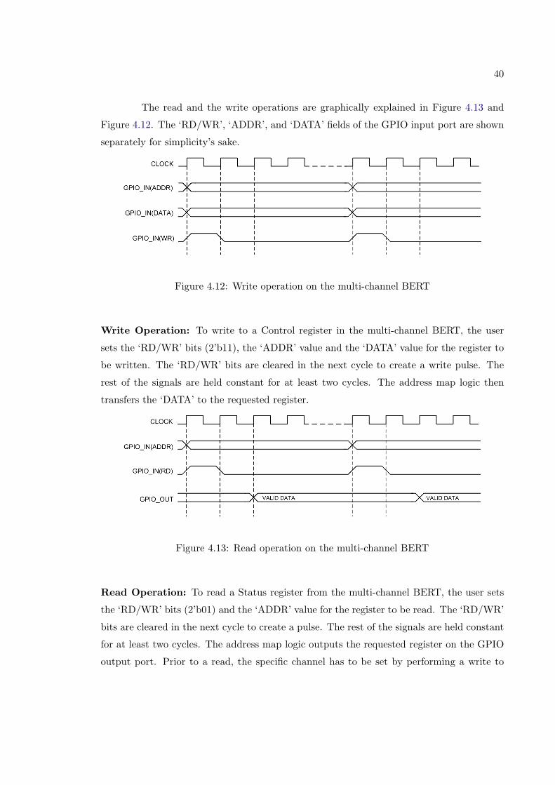
40
The read and the write operations are graphically explained in Figure 4.13 and
Figure 4.12. The ‘RD/WR’, ‘ADDR’, and ‘DATA’ fields of the GPIO input port are shown
separately for simplicity’s sake.
Figure 4.12: Write operation on the multi-channel BERT
Write Operation: To write to a Control register in the multi-channel BERT, the user
sets the ‘RD/WR’ bits (2’b11), the ‘ADDR’ value and the ‘DATA’ value for the register to
be written. The ‘RD/WR’ bits are cleared in the next cycle to create a write pulse. The
rest of the signals are held constant for at least two cycles. The address map logic then
transfers the ‘DATA’ to the requested register.
Figure 4.13: Read operation on the multi-channel BERT
Read Operation: To read a Status register from the multi-channel BERT, the user sets
the ‘RD/WR’ bits (2’b01) and the ‘ADDR’ value for the register to be read. The ‘RD/WR’
bits are cleared in the next cycle to create a pulse. The rest of the signals are held constant
for at least two cycles. The address map logic outputs the requested register on the GPIO
output port. Prior to a read, the specific channel has to be set by performing a write to

41
the channel control register.
4.2 PowerPC Subsystem
This section describes the design of the control plane of the BERT system. It uti-
lizes an embedded PowerPC processor, a 32-bit GPIO interface, data-side and instruction-
side block RAMs and their controllers, and a UART core. The 32-bit input/output interface
connects the multi-channel BERT design to the processor block, bridging the data plane
and the control plane. The processor reads the status and counter values from the BERT
design through the GPIO interface, and then sends the information to the RS232 host. The
user can configure and reset each channel, get information about the system and perform
BER measurements through the RS232 interface.
4.2.1 Embedded Development Kit
The PowerPC processor cores embedded in the Virtex II FPGAs can be employed
in a hardware design by using the EDK (Embedded Development Kit) [21]. EDK is a series
of software tools for designing embedded processor systems on Xilinx FPGAs. It consists
of a graphical interface that provides a simple flow to generate an embedded system. The
first step is to design a hardware platform that consists of the processor, the bus interfaces,
and the peripheral modules connected to the processor. This includes the development of
memory map for the peripherals, connections between the peripherals and the processor,
and definition of inputs and outputs.
After the hardware platform has been created, a software application to run on the
processor is developed. EDK provides various software libraries, containing specific high
level functions for common tasks, that can be used to enhance the software application.
The drivers for the peripheral components, that define the logical interface between the
processor and the peripheral, are also defined. The drivers for the standard peripherals are
provided in the EDK. A linker script, that defines how to link compiled sources together
for a target system, is also written.
After the creation of the hardware design and the software application to run on
the processors, simulations are carried out to verify the functionality of the system. This is

42
followed by the synthesis of the hardware design. The synthesized system along with the
compiled software is then downloaded to the FPGA.
Ultracontroller Module
Ultracontroller1 module is a PowerPC based design [9], provided by Xilinx Inc. It
is implemented as a 32-bit input / 32-bit output block that can be integrated with larger
systems to perform system monitoring and simple data manipulation tasks. It utilizes
several block RAMs for storing the instruction code and the data for the processor. Figure
4.14 shows the block diagram of the Ultracontroller design.
Figure 4.14: Block diagram of the Ultracontroller module
The use of OCM (On-Chip Memory) interface for instruction and data guarantees a
fixed latency of execution, as compared to the bus interface. This higher level of determinism
eases the integration of this module with the other logic on the FPGA using minimum
handshaking. The GPIO interface is implemented using the port B of the data-side block
RAM mapped as I/O. The interface implements reads and writes to the external hardware
by writing to dedicated locations in the block RAM. C-based drivers are provided to write
and read data from the GPIO port, in software. An added advantage of using the RAM
based interface is the ability to read back the previously written data. This allows the
flexibility of modifying individual bits at the output.
The use of memory mapped I/O in the module eliminates the need for the complex
bus structures and hence saves the logic resources on the FPGA. This module utilizes less1‘Ultracontroller’ is a registered trademark of Xilinx, Inc.

43
than 50 logic cells [9]. In addition to this, processor-based design allows the slow logic
to be implemented in the processor rather than in the FPGA fabric. According to [9], a
reference design implemented in fabric utilized 2400 logic cells as compared to 50 logic cells
plus 16K bytes of RAM in the processor-based design. The Ultracontroller module can run
at a maximum speed of 200 Mhz.
4.2.2 Processor System for BER Testing
We have modified and extended the Ultracontroller design, discussed above, to
fit our application. Certain peripherals like OPB-based UART, OPB-to-DCR bridge, and
DCM (Digital Clock Manager) are added. Figure 4.15 shows the block diagram of our
processor-based system.
Figure 4.15: Block diagram of the processor system
The DCM generates the clock for the processor system as well as the multi-channel
BERT module. The reset generation circuit generates synchronous reset signals for the
processor system as well as for the multi-channel BERT module to ensure proper initial-

44
ization. The PowerPC processor requires 3 different synchronous reset signals of at least 8
cycles duration of the processor clock. The reset signals for the PowerPC core are generated
by a reset module available in the EDK. More information on reset and clock generation is
discussed in the next section.
OPB-based UART
The UART core is provided in the EDK for communication across the RS232
interface [20]. It is capable of connecting to the OPB (On-chip Peripheral Bus) interface for
data transfer across the PowerPC processor and the RS232 host. It supports configurable
baud rate, parity and full-duplex transmission. It also contains 16-character transmit and
16-character receiver FIFO. Table 4.6 lists the features of the UART that are parameterized
to fit our application. The transmit FIFO, the receive FIFO, the status register and the
Table 4.6: Parameters for the OPB-based UART
Parameter Value Description
C CLK FREQ 75000000 Frequency of the OPB clock driving the UART mod-ule, in Hz.
C BAUDRATE 57600 Baud rate of the UART module in bits per second.
C DATA BITS 8 The number of bits to represent one character.
C USE PARITY 0 Determines whether parity is used or not.
C ODD PARITY 0 Determines whether parity is odd or even, only ifparity is used.
control register are address mapped at the offset of 0, +4, +8 and +12, respectively, from
the base address of this module in the system.
DCR-to-OPB bridge
The DCR (Device Control Register) bus interface supports the attachment of
on-chip registers for device control. Software can access these registers using the ‘mfdcr’
and ‘mtdcr’ instructions [14]. The DCR interface provides a mechanism for the processor
block to initialize and control peripheral devices that reside on the same FPGA chip. The
addressing used by these instructions is not memory mapped and thus does not interfere
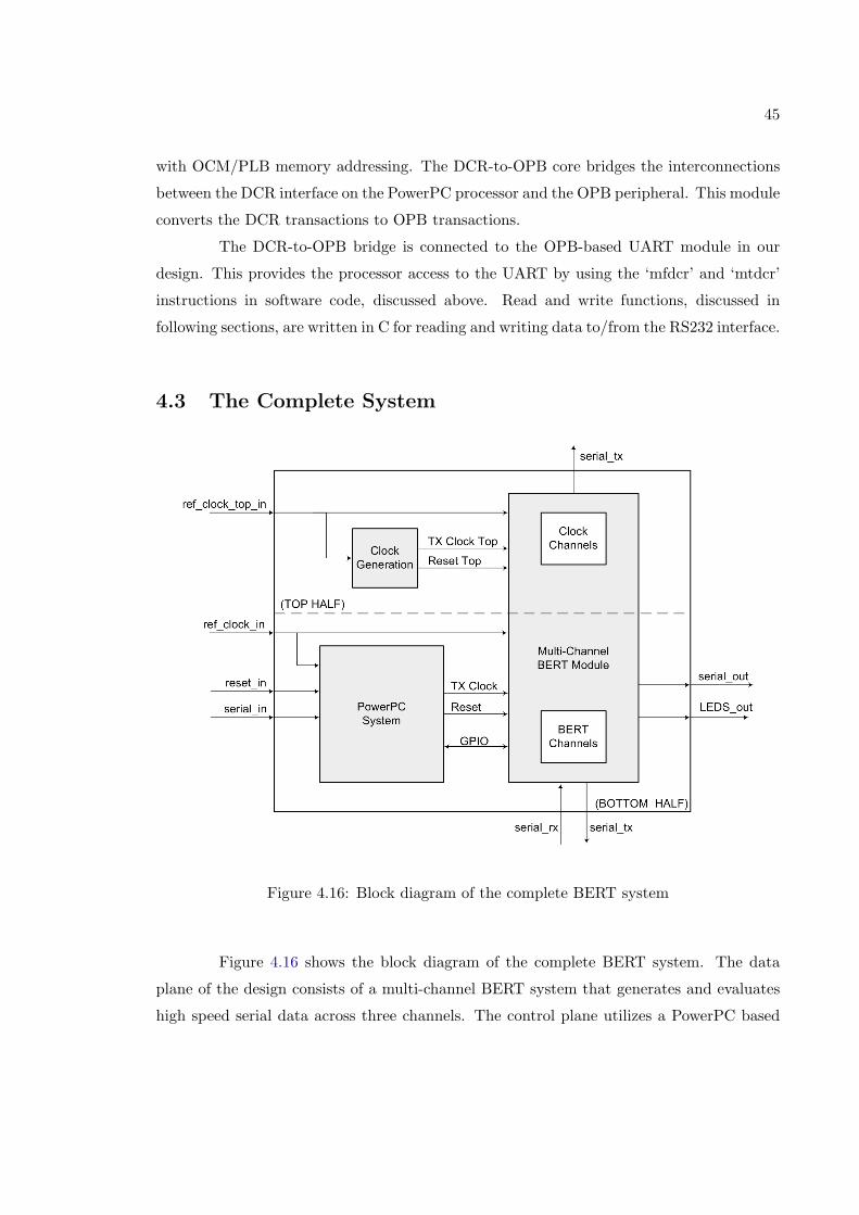
45
with OCM/PLB memory addressing. The DCR-to-OPB core bridges the interconnections
between the DCR interface on the PowerPC processor and the OPB peripheral. This module
converts the DCR transactions to OPB transactions.
The DCR-to-OPB bridge is connected to the OPB-based UART module in our
design. This provides the processor access to the UART by using the ‘mfdcr’ and ‘mtdcr’
instructions in software code, discussed above. Read and write functions, discussed in
following sections, are written in C for reading and writing data to/from the RS232 interface.
4.3 The Complete System
Figure 4.16: Block diagram of the complete BERT system
Figure 4.16 shows the block diagram of the complete BERT system. The data
plane of the design consists of a multi-channel BERT system that generates and evaluates
high speed serial data across three channels. The control plane utilizes a PowerPC based

46
system discussed above. The processor system reads the status and statistic values from the
data plane using the GPIO interface and sends the information to the RS232 port. It also
configures individual channels in the multi-channel BERT depending on the inputs received
from the RS232 interface.
The design is partitioned into the top and bottom halves, indicating the two regions
being clocked by two separate clocks. The control plane and the BERT channels in the
data plane reside on the bottom half, while the serial clock modules in the data plane are
placed on the top half. These are logical partitions which have significance only during the
implementation of the system on the FPGA. The individual BERT channels contain logic
that is driven by different clocks recovered from the received data. The outputs from these
logic modules are synchronized to the external clock in the multi-channel BERT module.
4.3.1 Clock Distribution
The reference clocks for the RocketIO transceivers use dedicated routing resources
and hence cannot be routed through the FPGA fabric to clock logic modules. Employing
separate clocks for the logic modules and the transceivers will result in synchronization
issues. Thus, there is a need to obtain phase-matched clocks to ensure reliable operation.
A DCM module embedded on the FPGA consists of delay elements and clock
synthesizing logic, which provides a phase-matched version of the input clock. The output
of the DCM is connected to a clock tree which distributes the clock to all registers and back
to the feedback pin of the DCM. The control circuit of the DCM adjusts the delays so that
the rising edges of the feedback clock align with the input clock. Once the edges of the
clocks are aligned, the DCM is locked, and both the input buffer delay and the clock skew
are reduced to zero. DCM also supports multiplication and division of the input clock. As
shown in Figure 4.17, the reference clocks are provided to the DCM module to generate
clocks for the control and data planes.
Two clock signals are generated, one for all the BERT channels and the control
plane while the other for all the serial clock generation modules. The output frequency
of the clock for the BERT channels is set to 1/2 the frequency of the reference clock.
This is done to reduce the serial rate of the BERT data by half when used in a source-
synchronous mode. For the clock generation transceivers the DCM clock is same frequency
as the reference clock. These output clocks are connected to global clock buffers to ensure
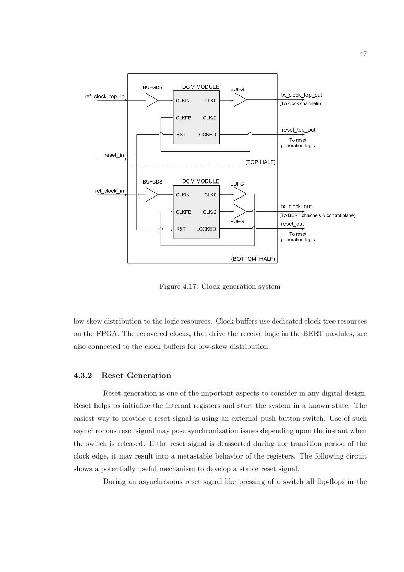
47
Figure 4.17: Clock generation system
low-skew distribution to the logic resources. Clock buffers use dedicated clock-tree resources
on the FPGA. The recovered clocks, that drive the receive logic in the BERT modules, are
also connected to the clock buffers for low-skew distribution.
4.3.2 Reset Generation
Reset generation is one of the important aspects to consider in any digital design.
Reset helps to initialize the internal registers and start the system in a known state. The
easiest way to provide a reset signal is using an external push button switch. Use of such
asynchronous reset signal may pose synchronization issues depending upon the instant when
the switch is released. If the reset signal is deasserted during the transition period of the
clock edge, it may result into a metastable behavior of the registers. The following circuit
shows a potentially useful mechanism to develop a stable reset signal.
During an asynchronous reset signal like pressing of a switch all flip-flops in the

48
Figure 4.18: Reset generation approach
chain are preset to ‘1’. Almost immediately, the last flip-flop of the chain then drives an
active reset to the system. When the external signal is deasserted, the reset does not go low
immediately. Instead, the chain begins to shift ‘0’ every clock cycle and eventually the reset
is deasserted synchronously with the clock. The number of flip-flops in the chain determines
the duration of the reset pulse issued to the system.
The are certain modules that impose specific requirements for the reset signal.
The RocketIO transceiver needs a reset pulse of 3 cycle duration to correctly initialize its
internal logic in an event of power-on, change of reference clock or a system reset. Similarly
the receive logic requires a reset signal that is synchronous to the recovered clocks. Figure
4.19 shows our logic for reset generation, based on the above approach.
4.4 Software Design
Once the hardware platform is defined and the peripherals are setup, an address
map is defined for all the peripherals connected to the processor. This helps the software
code to access the peripherals by using memory operations. Table 4.7 shows the address
map for our processor system.
4.4.1 Drivers
EDK contains software libraries and device drivers that provide standard C-based
functions to access the peripherals. For example, the drivers for the GPIO contain functions
to provide reads and writes to the 32-bit GPIO interface. Similarly, the drivers for UART
provides functions to read and write to the RS232 interface using ‘mtdcr’ and ‘mfdcr’

49
Figure 4.19: Reset generation in our system
Table 4.7: Address map for the peripherals
Peripheral Address Range Size
Base High
OPB-based UART 0xA0000000 0xA0000000 256 Bytes
DCR-to-OPB bridge 0xA0000000 0xA0000000 256 Bytes
GPIO Input Port 0xFE000004 0xFE000007 4 Bytes
GPIO Output Port 0xFE000000 0xFE000003 4 Bytes
Instruction-side BRAM 0xFFFFC000 0xFFFFFFFF 16 KBytes
Data-side BRAM 0xFE000000 0xFE001FFF 8 KBytes
instructions. The above drivers serve as base functions to develop customized subroutines
for the user application.

50
4.4.2 Software for BER testing
A software application, written in C, is developed to work with the hardware plat-
form. The software configures the BERT channels in the multi-channel BERT module and
also reads back the statistical values. We use a data structure to store the configuration
parameters and the BER data for all BERT channels. Such structure serves as an interme-
diate memory to transfer data from the control plane (the processor system) to the data
plane (multi-channel BERT). The software reads the status from the data plane to the data
structure and processes the data afterwards. On other hand, software reads user inputs
from the menu interface, stores them in the data structure, and then sends that data to the
data plane.
UART Software Code
As described earlier, drivers for the UART are provided to perform read and write
operations on the RS232 interface. Using these functions, more complex functions as listed
below, are developed.
1. UART Init: This function clears the transmit and the receive FIFOs in the OPB-
based UART module and initializes the module for non-interrupt based operation.
The syntax of this function is:
UART Init()
2. UART Write: This function takes an 8-bit character as an input, waits for the
previous transmission to get over and then sends the character to the RS232 port.
The syntax of this function is:
UART Write(char value)
3. UART Read: This function waits until a character is received from the RS232 port
and then returns the received character. The syntax of this function is:
char data = UART Read()
4. UART printf: This function is similar to the printf function in C, except that the
formatted output is written to the RS232 port. The syntax of this function is:
UART printf("%d %s..", value1, value2)
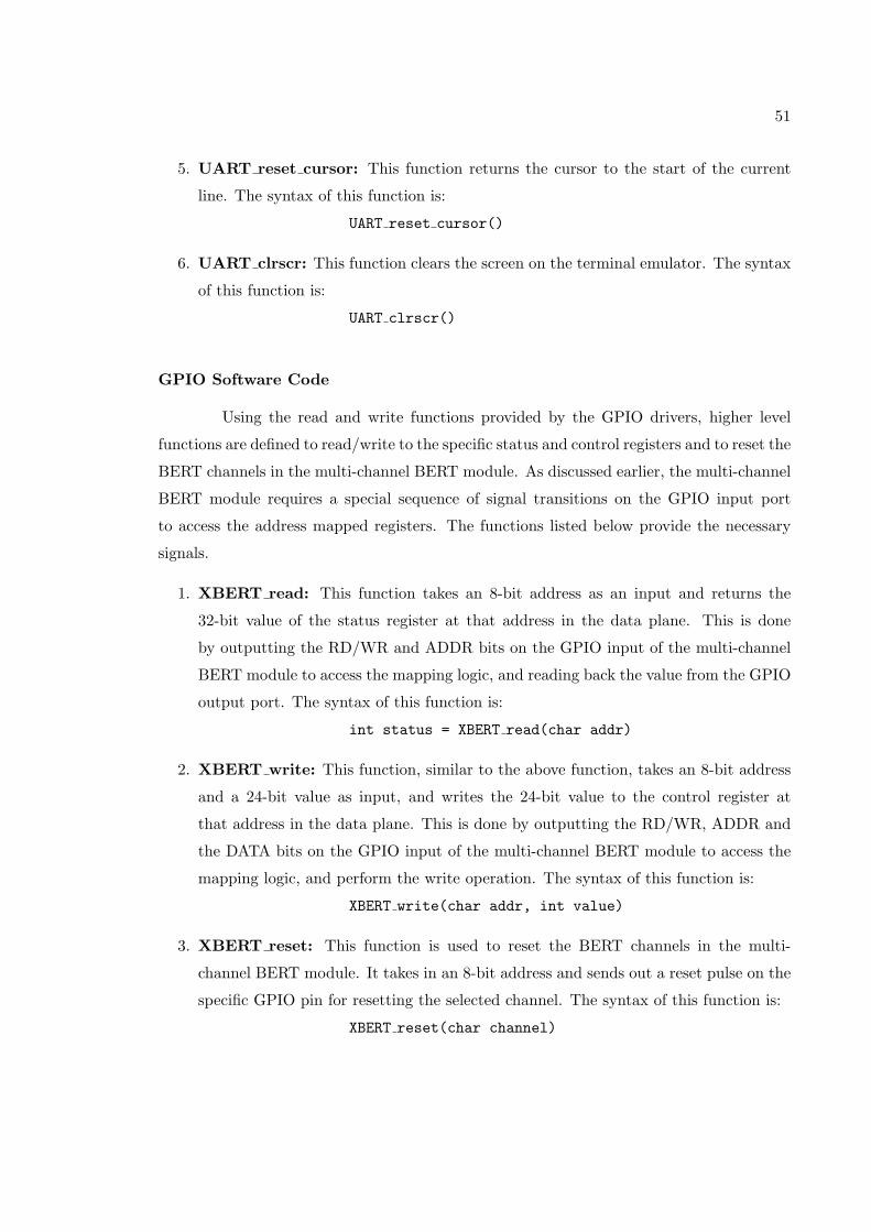
51
5. UART reset cursor: This function returns the cursor to the start of the current
line. The syntax of this function is:
UART reset cursor()
6. UART clrscr: This function clears the screen on the terminal emulator. The syntax
of this function is:
UART clrscr()
GPIO Software Code
Using the read and write functions provided by the GPIO drivers, higher level
functions are defined to read/write to the specific status and control registers and to reset the
BERT channels in the multi-channel BERT module. As discussed earlier, the multi-channel
BERT module requires a special sequence of signal transitions on the GPIO input port
to access the address mapped registers. The functions listed below provide the necessary
signals.
1. XBERT read: This function takes an 8-bit address as an input and returns the
32-bit value of the status register at that address in the data plane. This is done
by outputting the RD/WR and ADDR bits on the GPIO input of the multi-channel
BERT module to access the mapping logic, and reading back the value from the GPIO
output port. The syntax of this function is:
int status = XBERT read(char addr)
2. XBERT write: This function, similar to the above function, takes an 8-bit address
and a 24-bit value as input, and writes the 24-bit value to the control register at
that address in the data plane. This is done by outputting the RD/WR, ADDR and
the DATA bits on the GPIO input of the multi-channel BERT module to access the
mapping logic, and perform the write operation. The syntax of this function is:
XBERT write(char addr, int value)
3. XBERT reset: This function is used to reset the BERT channels in the multi-
channel BERT module. It takes in an 8-bit address and sends out a reset pulse on the
specific GPIO pin for resetting the selected channel. The syntax of this function is:
XBERT reset(char channel)

52
Top-Level Software Code
A menu based interface is provided for display on any terminal emulation software
using the RS232 interface. This interface provides easy navigational features to access and
configure the BERT test system. All the functions are coded as subroutines and are called
depending upon the user input. This approach of using subroutines is useful when the menu
interface needs to be removed during actual operation. The RS232 host that controls this
system will issue specific commands, which will directly calls the subroutines to perform
specific tasks, removing the need for the menu interface. The description of the major
subroutines is given below.
1. print chl stats: This function takes the channel number as input and reports the
current statistics of that BERT channel. This function reads the status registers
for the selected channel by performing read operations across the GPIO interface.
Once the registers are read, it extracts the information from these registers to output
meaningful values. It calculates and outputs the BER of the channel depending upon
the total number of frames received and total number of bit errors. Procedure to
calculate BER is described in following section. Error interval and type of pattern
currently being used is also reported. It outputs the link status bits such as search,
link, abort, tx inhibit, channel powered down, etc. The syntax of this function is:
print chl stats(char channel)
2. modify chl config: This function is used to modify the current configuration of the
BERT channels. Depending upon the specified channel this function performs write
operations across the GPIO interface to modify the control registers in the multi-
channel BERT system. The configurable parameters of a channel include the type
of pattern being evaluated, loopback mode, transmit inhibit and channel powerdown.
An important option is to artificially inject errors in the transmitted data stream.
Everytime this option is exercised, 20 bit-errors are inserted in the bit-stream. The
menu interface navigates the user to configure all these parameters and has the option
to check the modified configuration before applying the settings. The syntax of this
function is:
modify chl config(char channel)

53
Figure 4.20: Flow diagram of the BERT software application
Figure 4.20 shows the flow diagram of the complete software application for the
BERT system. After power-up or a system reset, the software performs the initialization
of the data structures and configures the channel with the initial set of patterns. After ini-
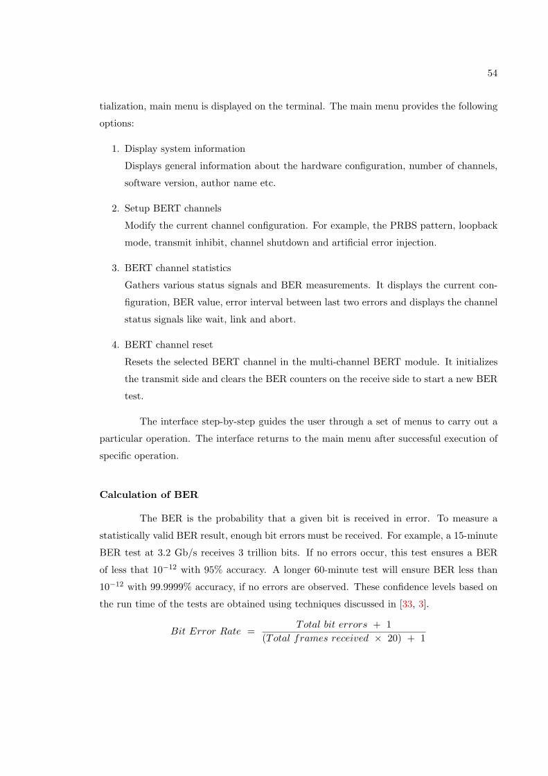
54
tialization, main menu is displayed on the terminal. The main menu provides the following
options:
1. Display system information
Displays general information about the hardware configuration, number of channels,
software version, author name etc.
2. Setup BERT channels
Modify the current channel configuration. For example, the PRBS pattern, loopback
mode, transmit inhibit, channel shutdown and artificial error injection.
3. BERT channel statistics
Gathers various status signals and BER measurements. It displays the current con-
figuration, BER value, error interval between last two errors and displays the channel
status signals like wait, link and abort.
4. BERT channel reset
Resets the selected BERT channel in the multi-channel BERT module. It initializes
the transmit side and clears the BER counters on the receive side to start a new BER
test.
The interface step-by-step guides the user through a set of menus to carry out a
particular operation. The interface returns to the main menu after successful execution of
specific operation.
Calculation of BER
The BER is the probability that a given bit is received in error. To measure a
statistically valid BER result, enough bit errors must be received. For example, a 15-minute
BER test at 3.2 Gb/s receives 3 trillion bits. If no errors occur, this test ensures a BER
of less that 10−12 with 95% accuracy. A longer 60-minute test will ensure BER less than
10−12 with 99.9999% accuracy, if no errors are observed. These confidence levels based on
the run time of the tests are obtained using techniques discussed in [33, 3].
Bit Error Rate =Total bit errors + 1
(Total frames received × 20) + 1

55
The software module calculates the BER in real-time using the counter (total frames re-
ceived and total bit errors) values of the BERT channels. To avoid the BER being zero
and give a realistic value of the BER, we assume that the next received frame has 1 bit-
error. Thus, the BER is never equal to zero and decreases as the test progresses and the
total number of received bits increases. BER is calculated only after the incoming data is
perfectly aligned with the expected data. Appropriate warning messages are generated by
the software if they are not aligned.
4.4.3 Memory Management
Memory requirements are specified in terms of how much memory is required for
storing the instructions, and how much memory is required for storing the data associated
with the program. A linker script is developed which indicates how the software application
and other components are stored in the memory. It defines the size of instruction memory,
data memory, stack and heap. Stack is used to store the temporary data during subroutine
calls. Heap is a portion of memory used during dynamic allocation in the software code.
The memory requirement of our software code is 14 KB for instructions and 5 KB for the
initialized data. Hence the size of the instruction memory is set to 16 KB and the data
memory is set to 8 KB. Since no dynamic allocation of memory is done in our software the
heap is set to its minimum value of 4 bytes. The size of the stack is set to 2048 bytes.
56
Chapter 5
Implementation and Results
In this chapter we describe the implementation of the BERT system on a Xilinx
Virtex II pro FPGA. Timing simulations are performed for major modules such as the trans-
mitter, the single-channel BERT and the multi-channel BERT. Implementation strategies
used to improve performance in terms of speed and area are discussed. The test setup of
the FPGA development board used for performance measurements is also described. We
also provide the actual power consumption values for the BERT design.
5.1 Timing Simulation
The HDL code for the logic modules is written using Verilog 2001 constructs. Ver-
ilog 2001 is a revised version of the original Verilog 95 standard and adds certain important
features to provide powerful constructs to develop reusable and scalable modules. The sim-
ulation process generally involves providing a stimulus to the module using a test bench
and verifying the outputs. Simulations are carried out at two levels in the design flow-
The behavioral simulation and the timing simulation. The behavioral simulation is used
to verify or simulate a module at a higher level of abstraction. This simulation is typically
performed to verify the syntax and the intended functionality. The timing simulation in-
volves simulation at gate level with the actual back-annotated timing delays after placing
and routing the design. The timing simulation provides a precise idea about the behavior
57
of the design in actual circuit. Xilinx provides a test bench waveform editor to graphically
develop the test benches for providing stimulus to the design. We have used this tool to
develop test benches for our HDL modules. Modelsim XE is used to simulate the design
and plot the waveforms.
The following waveform shows the timing simulation for the Transmitter module.
This module is used to provide parallel data to the RocketIOs. It contains a state machine
that sends out an initialization sequence composed of 218 Comma words followed by the
actual selected data pattern. In order to reduce the processing time and provide better
visual understanding, only 26 Comma words are transmitted for the initialization sequence,
in the simulation. As shown in the figure, the reset pin is initially asserted for a short
Figure 5.1: Simulation waveforms for the transmitter module
period of time. After the reset goes low, the module sends out the initialization sequence
composed of 26 Comma words (Comma value = 0x3E8E1). This is followed by the trans-
mission of the actual data pattern. The type of data pattern transmitted is selected by
the ‘pattern select in’ input. For this simulation the input is set to 7, which indicates the
transmission of PRBS20 pattern (Table 4.1).
The function of the ‘error insert in’ input can be seen in Figure 5.2 by using a
constant data pattern. The assertion of this input causes the module to invert all the bits
at the output. This feature is used to artificially insert errors in the data stream and hence
test the integrity of the receive logic. As shown above, a constant user-defined data pattern
(0xc1554 = 0b11000001010101010100) is transmitted following the initialization sequence.
When the ‘error insert in’ is asserted all the bits of the output data are inverted (0x3eaab
= 0b00111110101010101011).

58
Figure 5.2: Inserting error in the transmitted data stream
5.1.1 Simulation of RocketIOs
RocketIOs are customized high-speed transceivers embedded on the FPGA. They
are not regular library elements and hence cannot be simulated directly using the above
approach. Special models known as SmartModels are used to simulate the RocketIOs.
SmartModels are an encrypted version of the actual HDL code. These models allow the
user to simulate the actual functionality without having access to the code itself. They are
often behavioral description of the actual circuit. SmartModel wrappers are instantiated
in the design and an HDL simulator that supports the SWIFT interface is used to perform
simulations. SmartModels also contain back-annotated timing information and hence can
be successfully used for timing simulations.
The single-channel BERT module consists of the Transmitter module, the Receiver
module, the asynchronous FIFO and the RocketIO transceiver. The data patterns from the
Transmitter are provided to the RocketIO transceiver for serialization. For simulations, the
transceiver is operated in a loopback mode i.e. the serial transmitter output is internally
connected to the serial receiver input. The transceiver takes the serial data and provides the
deserialized data to the Receiver, which generates the necessary control signals and BER
statistics. The FIFO synchronizes the output of the receiver with respect to the transmit
clock. The simulation waveforms for the single-channel BERT are shown in Figure 5.3. For
simplicity’s sake, the signals are grouped with respect to the module which they internally
belong.

59
Figure 5.3: Simulation waveforms for the single-channel BERT
1. Transmitter:
As shown in the figure, Transmitter outputs the initialization pattern followed by the
PRBS data pattern (TX data). An edge detection circuit generates a pulse whenever
the ‘Error Insert’ pin is toggled (highlighted). This pulse is provided to the transmit-
ter to generate a single error frame, thus introducing 20-bit errors in the transmission.

60
2. RocketIO:
The RocketIO module is provided with two reference clocks (Ref Clock and Ref
Clock2), which are selectable using the ‘Clock Sel’ input. For the current simula-
tion the ‘Ref Clock’ is selected while ‘Ref Clock2’ is tied to zero. The RocketIO sends
out the serial data on the ‘Serial TX’ pins. Since the design is running in loopback
mode, the ‘Serial RX’ inputs are not driven. The ‘Comma Detect’ Signal is asserted
every time a bit-pattern matching the Comma word is received. As shown, this sig-
nal goes high initially for a long time, indicating an initialization sequence from the
transmitter.
3. Receiver:
The receiver gets the parallel data deserialized by the RocketIOs. It also receives the
‘Comma Detect’ signal mentioned above. If a sequence of 32 (64 in actual) consecutive
Comma words is detected then the receive logic is initialized and the module asserts
the ‘Wait’ signal indicating that it is ready to accept the data pattern. When a valid
data stream is detected, the receiver asserts the ‘Lock’ signal and starts the BER
measurements. The error frame inserted in the transmit side and its corresponding
detection by the receive logic is highlighted. As shown, the BER counters are updated
with the error values.
4. FIFO:
The BER counters and the status signals in the Receiver are synchronous with the
clock recovered by the RocketIO. These data signals are passed through this asyn-
chronous FIFO module to make them synchronous to the ‘TX clock’.
5.1.2 Multi-channel BERT module
The multi-channel BERT module instantiates three BERT channels and two clock
channels. It also contains address mapped registers that provide access to the internal
control and status registers. The BERT channels can be configured independently through
the GPIO interface. Similar to the simulation of single-channel BERT, all the channels
are operated in loopback mode. The data rate of the BERT channels is half that of the
clock channels, to support source-synchronous interface. The functionality of this module
is verified by issuing commands through the GPIO input. The simulation waveforms for

61
the multi-channel BERT module are as shown in Figure 5.4
Figure 5.4: Simulation waveforms for the multi-channel BERT
For simplicity, the signals have been grouped according to the module they belong
to. The individual fields (GPIO RD, GPIO WR, GPIO ADDR, GPIO DATA) from the 32-
bit GPIO input are shown separately. The BERT channels have locked with their respective
incoming data, indicated by the assertion of the ‘Lock’ signal. Specific commands are issued
to read the status register and write to the control registers (4.3). These commands, shown
in the waveform by red numerals, are listed as follows:
1. Write: This operation writes 0x000000 to the control register at address 3, to select
channel 1 for further operations.
2. Read: This operation reads the status register at address 3, which contains the total
frames received by channel 1, and sends it to the GPIO output.
3. Write: This operation writes 0x00012c to the control register at address 0, toggling
the ‘error insert’ pin for channel 1 and hence inserts 20 bit-errors in the transmitted
stream .
4. Read: This operation reads the status register at address 1, which contains the total
bit errors received by channel 1, and sends it to the GPIO output. The result on the
62
GPIO output confirms the success of the previous operation.
5. Write: This operation writes 0x000001 to the control register at address 3, to select
channel 2 for further operations.
6. Write: This operation sends 0x02000000 to the GPIO input, toggling the reset pin of
channel 2.
7. Read: This operation reads the status register at address 3, which contains the total
frames received by channel 2. As we can see channel 2 is still waiting for a lock after
the previous reset operation and hence returns 0 on the GPIO output.
5.2 Synthesis and Implementation
Synthesis is the process of converting an HDL description of a design into an
optimized gate-level representation. FPGA synthesis involves mapping the HDL modules
to the FPGA logic resources such as LUTs, block RAMs, flip flops etc. The synthesis
tool generates the area and timing reports which provide a preliminary estimate of the
device utilization and performance. The device utilization and performance report lists the
compiled cells in the design, as well as information on how the design is mapped in the
FPGA. The actual utilization and timing performance are available after the design has
been placed and routed on the FPGA.
Synthesis is guided by several user-configurable settings. These settings include
optimization effort, area goal, timing goal, resource sharing, register retiming etc. The syn-
thesis tool provides default settings for optimum performance over generalized applications.
However, to get the best results these settings have to be fine-tuned for the particular appli-
cation. For example, resource sharing is an optimization technique that is used to improve
performance by reducing the gate count and the routing congestion. However, resource
sharing should not be used for timing critical paths. The complete BERT design is syn-
thesized using the XST (Xilinx Synthesis Technology) and the area and timing report is as
shown below.
=========================================================================Device utilization summary:---------------------------
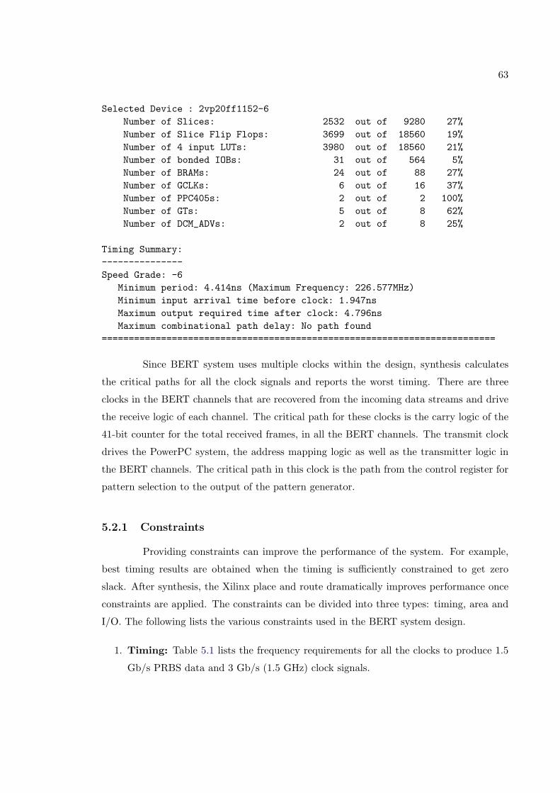
63
Selected Device : 2vp20ff1152-6Number of Slices: 2532 out of 9280 27%Number of Slice Flip Flops: 3699 out of 18560 19%Number of 4 input LUTs: 3980 out of 18560 21%Number of bonded IOBs: 31 out of 564 5%Number of BRAMs: 24 out of 88 27%Number of GCLKs: 6 out of 16 37%Number of PPC405s: 2 out of 2 100%Number of GTs: 5 out of 8 62%Number of DCM_ADVs: 2 out of 8 25%
Timing Summary:---------------Speed Grade: -6
Minimum period: 4.414ns (Maximum Frequency: 226.577MHz)Minimum input arrival time before clock: 1.947nsMaximum output required time after clock: 4.796nsMaximum combinational path delay: No path found
=========================================================================
Since BERT system uses multiple clocks within the design, synthesis calculates
the critical paths for all the clock signals and reports the worst timing. There are three
clocks in the BERT channels that are recovered from the incoming data streams and drive
the receive logic of each channel. The critical path for these clocks is the carry logic of the
41-bit counter for the total received frames, in all the BERT channels. The transmit clock
drives the PowerPC system, the address mapping logic as well as the transmitter logic in
the BERT channels. The critical path in this clock is the path from the control register for
pattern selection to the output of the pattern generator.
5.2.1 Constraints
Providing constraints can improve the performance of the system. For example,
best timing results are obtained when the timing is sufficiently constrained to get zero
slack. After synthesis, the Xilinx place and route dramatically improves performance once
constraints are applied. The constraints can be divided into three types: timing, area and
I/O. The following lists the various constraints used in the BERT system design.
1. Timing: Table 5.1 lists the frequency requirements for all the clocks to produce 1.5
Gb/s PRBS data and 3 Gb/s (1.5 GHz) clock signals.
64
Table 5.1: Timing requirements for the BERT system
Clock Signal Frequency Description
Ref Clock 150 MHz Drives the transceivers located on the bottom half ofthe FPGA.
TX Clock 75 MHz Drives the BERT channels as well as the PowerPCsystem located on the bottom half of the FPGA.The serial data rate of the BERT channels is: (TXClock*20).
Ref Clock Top 150 MHz Drives the transceivers located on the top half of theFPGA.
TX Clock Top 150 MHz Drives the serial clock channels located on the tophalf of the FPGA. The serial data rate of the clockchannels is: (TX Clock Top*20).
RX Clocks 75 MHz Drives the receive logic in the BERT channels. Thefrequency is same as the TX clock.
These values dictate the specifications required for the current BERT system and are
limited due to the maximum frequency that is supported by the current RocketIOs.
To provide the flexibility of porting this design to the newer technologies capable of
handling higher frequencies, the BERT design is constrained with higher timing values
than those shown above. Table 5.2 lists the timing constraints applied to the BERT
system.
Table 5.2: Timing constraints for the BERT system
Clock Signal Constraint
TX Clock 200 MHz
RX Clocks 200 MHz
2. Area: The area constraints include the assignment of the logic elements to a particular
resource on the FPGA. For example, placing the instruction-side and data-side block
RAM elements, used in the PowerPC system, close to the processor would improve
performance. Other area constraints include grouping of logic driven by the same
clock, placing the transmit and receive logic close to the transceivers, specifying the
clock trees for all the clocks used in the design etc. Table 5.3 lists the area constraints

65
applied to the BERT system.
Table 5.3: Area constraints for the BERT system
Logic Constraint Constraint Description
BERT Channel 1 Slices(X0Y0-X30Y50) Specifies the bounding box of the resourcesBERT Channel 2 Slices(X31Y0-X60Y50) located in the bottom half of the FPGA toBERT Channel 3 Slices(X61Y0-X91Y50) implemtent BERT channels.
RX Clock 1 BUFGMUX5S Specifies the clock buffers to be used for theRX Clock 2 BUFGMUX7S recovered clocks. The specified buffers areRX Clock 3 BUFGMUX3S located on the bottom edge of the FPGA.
The above values are specified in the constraints file before implementation. Other
constraints like the placement of the block RAMs near the processor and the placement
of the comma alignment modules near the transceivers are specified graphically in the
constraints editor.
Table 5.4: I/O constraints for the BERT system
I/O Location I/O DescriptionStandard
Leds[0:5] AK7, AK6,AH9, AG9,AK29, AK28
LVCMOS25 Connects to the LEDs on the board.
Refclk AL18, AK18 LVDS25 Differential clock inputs for the bottom half.
Refclk Top J18, H18 LVDS25 Differential clock inputs for the top half.
Reset AL6 LVCMOS25 Asynchronous system reset.
Serial In AE11 LVCMOS25 Serial Input from the RS232 port.
Serial Out AF10 LVCMOS25 Serial Output to the RS232 port.
3. I/O: These constraints are used to specify the pin location on the FPGA, type of
voltage standard, drive strength of the outputs etc., for the system I/Os. Table 5.4
lists the area constraints applied to the BERT system.

66
5.2.2 Results
The implementation is carried out using the constraints mentioned above. Incre-
mental phases are run with the timing constraints relaxed or tightened by 5% until the slack
is 0. The area constraints are also relaxed or tightened during each phase depending upon
the result of the previous phase. The optimization setting for the place-and-route tool is
set to medium effort, to reduce run time. Table 5.5 shows the post-route timing results for
the TX and RX clocks.
Table 5.5: Timing results for the BERT system
Clock Signal Required Maximum Maximum FanoutFrequency Frequency Skew
TX Clock 75 MHz 180 MHz 0.821 ns 1066
RX Clock 1 75 MHz 200 MHz 0.553 ns 412
RX Clock 2 75 MHz 200 MHz 0.760 ns 412
RX Clock 3 75 MHz 200 MHz 0.702 ns 412
The resource utilization summary for the entire BERT system after placing and routing is
as given below.
=========================================================================Logic Utilization:Selected Device : 2vp20ff1152-6
Number of occupied Slices: 3,065 out of 9,280 33%Number of Slice Flip Flops: 3,666 out of 18,560 19%Number of 4 input LUTs: 3,458 out of 18,560 18%Number of bonded IOBs: 15 out of 564 2%Number of Block RAMs: 24 out of 88 27%Number of GCLKs: 6 out of 16 37%Number of PPC405s: 2 out of 2 100%Number of DCMs: 2 out of 8 25%Number of GTs: 5 out of 8 62%
=========================================================================
Figure 6.1 shows the final floorplan for the entire system placed on a Virtex II
pro FPGA. The BERT channels, clock channels, PowerPCs, Block RAMS, RocketIO trans-
ceivers for each channel, and DCM are shown in the figure. As discussed in earlier sections,
all the BERT channels are implemented on the bottom half of the FPGA while the clock

67
Figure 5.5: Final floorplan of the implemented design
channels are implemented in the top half. The PowerPC processor on the right half of the
FPGA is used for the BERT system. The layout of each channel contains several empty

68
spaces, indicating a poor placement. However, this has been done on purpose to improve
timing performance of the system. A tightly packed system would mean extra routing
congestion, which may result into longer paths and hence affect timing. Since the design
utilizes only 30% of the area, the area constraints are relaxed by a small amount to ensure
efficient routing for better timing performance.
As shown in the floorplan, the instruction-side and the data-side block RAMs
are placed near the PowerPC processor to achieve better performance. The block RAMs
used for the FIFO modules in the BERT channels are placed close to the respective BERT
channels.
5.3 Board-Level Testing
The process of implementation is followed by the generation of a bit file to con-
figure and test the design on the FPGA. An FPGA development board is used to verify
the functionality of the BERT design. The board also serves as a prototype of the self-test
vehicle. Since FPGAs have volatile memory, the configuration information is lost when the
power is switched off. In order to prevent running of the configuration process everytime
during power-up, a PROM module present on the development board is used to store the
configuration data. During power-up, the PROM initializes the FPGA with the configura-
tion data.
The configuration data contains information about the gate-level hardware of the
design. The BERT design consists of PowerPC system along with the logic resources. The
software for the processor is compiled and an executable file is generated. In order to
function correctly, the software must also be stored in the specific block RAMs. A utility
called ‘DATA2BRAM’ [11] is used to develop configuration data for the block RAMs from
the executable file. This data is combined with the hardware configuration file by the above
utility. This complete configuration file is then sent to the PROM or the FPGA using ISE
tools. A JTAG cable is used for programming.
The development board contains voltage regulators, crystal oscillators, SMA con-
nectors for the high speed RocketIO transceivers and other miscellaneous modules for hard-
ware characterization. SMA connectors for using external differential clocks are also pro-
vided. The test setup to characterize the BERT system is as shown in Figure 5.6. The
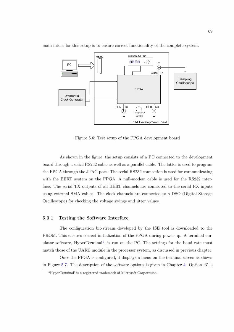
69
main intent for this setup is to ensure correct functionality of the complete system.
Figure 5.6: Test setup of the FPGA development board
As shown in the figure, the setup consists of a PC connected to the development
board through a serial RS232 cable as well as a parallel cable. The latter is used to program
the FPGA through the JTAG port. The serial RS232 connection is used for communicating
with the BERT system on the FPGA. A null-modem cable is used for the RS232 inter-
face. The serial TX outputs of all BERT channels are connected to the serial RX inputs
using external SMA cables. The clock channels are connected to a DSO (Digital Storage
Oscilloscope) for checking the voltage swings and jitter values.
5.3.1 Testing the Software Interface
The configuration bit-stream developed by the ISE tool is downloaded to the
PROM. This ensures correct initialization of the FPGA during power-up. A terminal em-
ulator software, HyperTerminal1, is run on the PC. The settings for the baud rate must
match those of the UART module in the processor system, as discussed in previous chapter.
Once the FPGA is configured, it displays a menu on the terminal screen as shown
in Figure 5.7. The description of the software options is given in Chapter 4. Option ‘3’ is1‘HyperTerminal’ is a registered trademark of Microsoft Corporation.

70
Figure 5.7: Main menu of the BERT system
selected from the main menu to view channel statistics. Entering the channel number in
the next menu will display the BER statistics of that channel, as shown in Figure 5.8.
Figure 5.8: Channel statistics
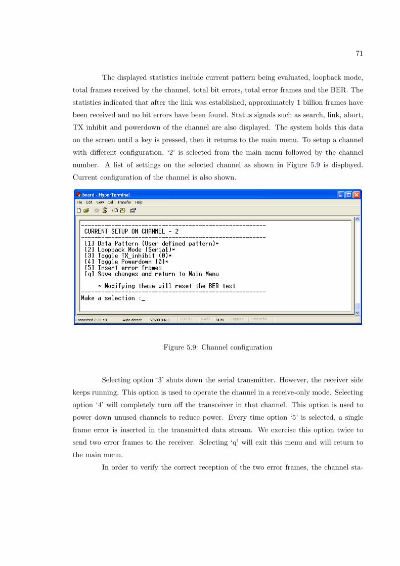
71
The displayed statistics include current pattern being evaluated, loopback mode,
total frames received by the channel, total bit errors, total error frames and the BER. The
statistics indicated that after the link was established, approximately 1 billion frames have
been received and no bit errors have been found. Status signals such as search, link, abort,
TX inhibit and powerdown of the channel are also displayed. The system holds this data
on the screen until a key is pressed, then it returns to the main menu. To setup a channel
with different configuration, ‘2’ is selected from the main menu followed by the channel
number. A list of settings on the selected channel as shown in Figure 5.9 is displayed.
Current configuration of the channel is also shown.
Figure 5.9: Channel configuration
Selecting option ‘3’ shuts down the serial transmitter. However, the receiver side
keeps running. This option is used to operate the channel in a receive-only mode. Selecting
option ‘4’ will completely turn off the transceiver in that channel. This option is used to
power down unused channels to reduce power. Every time option ‘5’ is selected, a single
frame error is inserted in the transmitted data stream. We exercise this option twice to
send two error frames to the receiver. Selecting ‘q’ will exit this menu and will return to
the main menu.
In order to verify the correct reception of the two error frames, the channel sta-

72
Figure 5.10: Verifying the reception of error frames
Figure 5.11: Pattern select menu
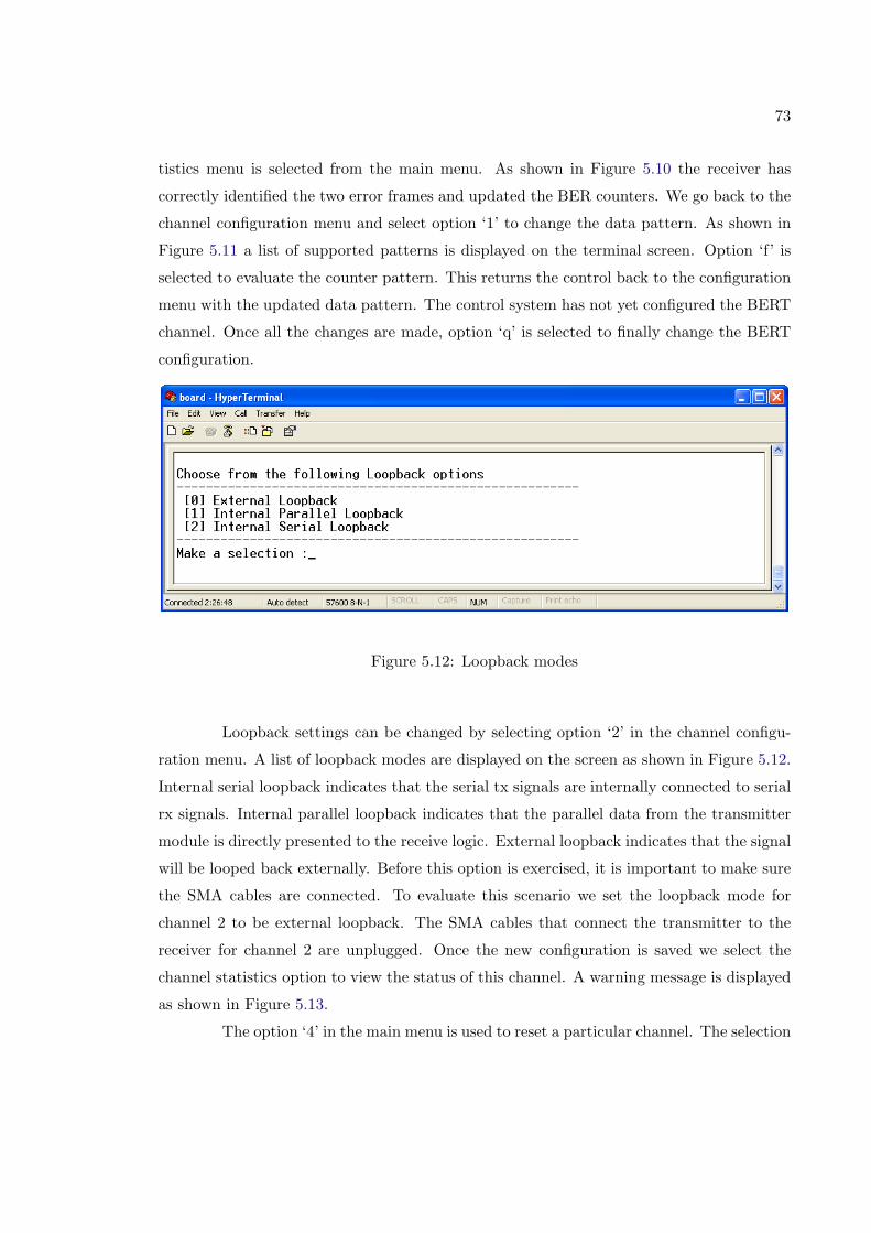
73
tistics menu is selected from the main menu. As shown in Figure 5.10 the receiver has
correctly identified the two error frames and updated the BER counters. We go back to the
channel configuration menu and select option ‘1’ to change the data pattern. As shown in
Figure 5.11 a list of supported patterns is displayed on the terminal screen. Option ‘f’ is
selected to evaluate the counter pattern. This returns the control back to the configuration
menu with the updated data pattern. The control system has not yet configured the BERT
channel. Once all the changes are made, option ‘q’ is selected to finally change the BERT
configuration.
Figure 5.12: Loopback modes
Loopback settings can be changed by selecting option ‘2’ in the channel configu-
ration menu. A list of loopback modes are displayed on the screen as shown in Figure 5.12.
Internal serial loopback indicates that the serial tx signals are internally connected to serial
rx signals. Internal parallel loopback indicates that the parallel data from the transmitter
module is directly presented to the receive logic. External loopback indicates that the signal
will be looped back externally. Before this option is exercised, it is important to make sure
the SMA cables are connected. To evaluate this scenario we set the loopback mode for
channel 2 to be external loopback. The SMA cables that connect the transmitter to the
receiver for channel 2 are unplugged. Once the new configuration is saved we select the
channel statistics option to view the status of this channel. A warning message is displayed
as shown in Figure 5.13.
The option ‘4’ in the main menu is used to reset a particular channel. The selection
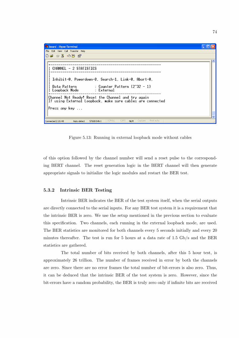
74
Figure 5.13: Running in external loopback mode without cables
of this option followed by the channel number will send a reset pulse to the correspond-
ing BERT channel. The reset generation logic in the BERT channel will then generate
appropriate signals to initialize the logic modules and restart the BER test.
5.3.2 Intrinsic BER Testing
Intrinsic BER indicates the BER of the test system itself, when the serial outputs
are directly connected to the serial inputs. For any BER test system it is a requirement that
the intrinsic BER is zero. We use the setup mentioned in the previous section to evaluate
this specification. Two channels, each running in the external loopback mode, are used.
The BER statistics are monitored for both channels every 5 seconds initially and every 20
minutes thereafter. The test is run for 5 hours at a data rate of 1.5 Gb/s and the BER
statistics are gathered.
The total number of bits received by both channels, after this 5 hour test, is
approximately 26 trillion. The number of frames received in error by both the channels
are zero. Since there are no error frames the total number of bit-errors is also zero. Thus,
it can be deduced that the intrinsic BER of the test system is zero. However, since the
bit-errors have a random probability, the BER is truly zero only if infinite bits are received

75
without error. Hence, a confidence level needs to be established as mentioned in [33, 3].
The confidence level is defined as the probability that the actual probability of an event
is better than a specified level. The confidence level equations for the current statistics
lead to the conclusion that the intrinsic BER is less than 10−12 with a confidence level of
99.9999% or that the intrinsic BER is less than 10−13 with a confidence level of 93%. Since
our software calculates the BER using an assumption that the next received bit is in error
the accuracy of the reported BER value increases as the number of received bits increases.
This can be explained by the graph shown in Figure 5.14.
Figure 5.14: Plot for the intrinsic BER
5.3.3 Waveform Observation
The above test setup is modified for performing electrical measurements. The
transmitter outputs from the BERT channels as well as the clock channels are connected

76
to a high speed sampling oscilloscope. The output waveforms are observed for verifying the
source-synchronous operation, voltage swings and jitter values. Figure 5.15 shows the eye
diagram for the data and clock outputs from the FPGA. The data rate is 1.5 Gb/s and
differential voltage swing is 400 mV p-p.
Figure 5.15: Eye diagram of the PRBS data and corresponding clock
The clock signal is running at 3 Gb/s. The shape of the waveform is sinusoidal
rather than a square wave. This is a limitation of the development board. The BGA package
of the FPGA is socket-mounted and the signal from the RocketIOs have to travel through
three level of interconnects (solder balls, socket pin, wire connection to the board) before it
comes out at the SMA pins. The parasitics of these interconnects contribute to the slowing
of the rise time of the signal. The actual system will have the FPGA directly soldered on
the PCB and will ensure improved performance.
Figure 5.16 and 5.17 shows the jitter measurements for the BERT data and clock
signals respectively. The peak-to-peak jitter on the data signals is 44 ps, while the peak-
to-peak jitter on the clock signals is 24 ps.

77
Figure 5.16: Jitter calculation for the PRBS data
Figure 5.17: Jitter calculation for the serial clock
5.3.4 Power Consumption
We have initially performed the pre-implementation analysis of the power con-
sumption using software tools. In this section, we present the actual power values for
the various voltage sources using the FPGA development board. The FPGA development
board provides an option of connecting separate external voltages sources for each individ-
ual power supply used on the board. The BERT design is configured in the FPGA and the
power values are calculated by measuring currents from the various power supplies. Figure
5.18 shows the test setup for the power measurements.
As shown in the figure, the development board provides an option of connecting

78
Figure 5.18: Setup for power measurement
external power supplies by changing certain jumper settings. To have a fair comparison
with the previous power values here is the summary of the resource utilization in our final
design.
1. The design utilizes 30% of the logic resources.
2. The operating frequency is 75 Mhz for the logic as well as the processor.
3. The design uses 50% of the block RAM resources.
4. Uses 3 full-duplex RocketIO transceivers running at 1.5 Gb/s.
5. Uses 2 transmit-only RocketIO transceivers running at 3 Gb/s.
6. A total of 15 general purpose digital I/Os for the FPGA.
Table 5.6 provides the values for the total power consumption in the system.
Including the power consumed by the FPGA, the power consumed by the other components
(vcc3) on the board is also shown. Though these figures represent actual measured values,
the power consumption in the system would also include the power dissipated in the voltage
converters. Use of high efficiency voltage regulators will help keep the power dissipation to
the minimum.

79
Table 5.6: Actual values for the power consumption
VOLTAGE SOURCE VOLTAGE POWER
Core supply (Vccint) 1.5 V 489 mW
Auxiliary + I/O supply (Vccaux + Vcco) 2.5 V 382 mW
RocketIO Supply 2.5 V 1315 mW
Total Power usage by FGPA 2186 mW
Board Supply (Vcc3) 3.3 V 430 mW
Total Power 2616 mW

80
Chapter 6
Printed Circuit Board Design
This chapter describes the design of a customized PCB (Printed Circuit Board)
for the BERT system. The board will serve as a stand-alone system capable of performing
BER measurements and connecting to an RS232 interface. This chapter also describes the
process of selecting optimum components for the VRMs (Voltage Regulation Module), clock
oscillators, high-speed connectors etc. A rough placement of the components to approximate
the dimensions of the final system, is included. Finally, considerations and guidelines for
efficient layout of the PCB are discussed.
6.1 Schematic Design
FPGA-based systems require special attention to the design of the power delivery
system, clock generators and peripherals. The requirements for the supporting components
greatly depend on the FPGA’s internal logic and I/Os, which are configured by the designer.
The BERT system is prototyped using a development board which uses a Xilinx Virtex II
Pro (XC2VP20) FPGA. The logic utilization by the BERT system is approximately 30%
of the total resources available on this particular FPGA and hence a lower grade FPGA,
having lesser resources, can be used for the current application. However, in order to allow
flexibility of extending the BERT system to a more complex test application, we will use
the above mentioned FPGA in the design of the customized system.
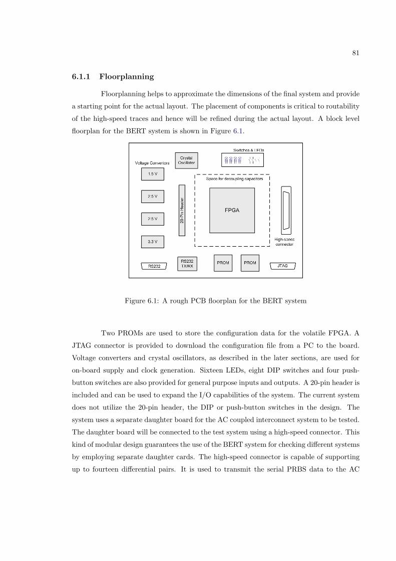
81
6.1.1 Floorplanning
Floorplanning helps to approximate the dimensions of the final system and provide
a starting point for the actual layout. The placement of components is critical to routability
of the high-speed traces and hence will be refined during the actual layout. A block level
floorplan for the BERT system is shown in Figure 6.1.
Figure 6.1: A rough PCB floorplan for the BERT system
Two PROMs are used to store the configuration data for the volatile FPGA. A
JTAG connector is provided to download the configuration file from a PC to the board.
Voltage converters and crystal oscillators, as described in the later sections, are used for
on-board supply and clock generation. Sixteen LEDs, eight DIP switches and four push-
button switches are also provided for general purpose inputs and outputs. A 20-pin header is
included and can be used to expand the I/O capabilities of the system. The current system
does not utilize the 20-pin header, the DIP or push-button switches in the design. The
system uses a separate daughter board for the AC coupled interconnect system to be tested.
The daughter board will be connected to the test system using a high-speed connector. This
kind of modular design guarantees the use of the BERT system for checking different systems
by employing separate daughter cards. The high-speed connector is capable of supporting
up to fourteen differential pairs. It is used to transmit the serial PRBS data to the AC

82
coupled interconnects and receive back the data for examination. It also carries a 5 V
supply signal to provide power to the electronics on the daughter board. A similar matched
connector will also be included on the daughter card such that it can be directly connected
to the test system. An assembly of the test system along with the daughter card is shown
in Figure 6.2.
Figure 6.2: Cross-section of test system and daughter card assembly
The I/Os of the FPGA can be divided into three categories: high-speed serial
I/Os, differential clock and LED I/Os, and asynchronous I/Os such as reset and RS232
signals. The floorplan is developed, taking into consideration approximate routing for the
above I/Os. All single-ended I/Os are set to 2.5 V LVCMOS voltage standard, while all
differential I/Os are set to 2.5 V LVDS signaling. On-chip termination is applied for all the
FPGA I/Os to avoid placing termination resistors on the board, hence saving board space.
All the above constraints are specified during the implementation phase of the design. They
can be refined depending on the electrical and physical parameters of the actual layout. The
components selected for implementation of the BERT system on the PCB are listed in Table
6.1.
6.1.2 Voltage Regulation Modules
The VRMs on the BERT system incorporate an input stage consisting of a switch-
ing regulator with a voltage range of 8 V to 40 V. This ensures the usability of the system
for a multitude of applications involving different voltage supplies. The entire power sup-
ply system consists of multiple voltage converters. The switching regulator delivers a 5 V
supply to the subsequent voltage regulators. These smaller regulators are linear voltage
converters which provide various supplies for the FPGA and other modules on the board.
The top-level diagram of the VRM subsystem is shown in Figure 6.3.
The SMPS (Switched Mode Power Supply) circuitry is based on a LM2678 chip
from National Semiconductor, which provides a 5V/5Amp supply. This chip belongs to

83
Table 6.1: List of components for the BERT system
Part Name Part Supplier RemarksNumber
Virtex II pro FPGA XC2VP20 Xilinx Inc. FPGA with embedded PowerPCprocessor and serial transceivers.
Storage PROM XC18V04 Xilinx Inc. Used to hold the configurationdata.
RS232 Transceivers MAX3338 Maxim Inc. Used to convert the voltagesbetween RS232 port and theFPGA.
Crystal Oscillator EG2121 Epson Electronics Oscillator for clock generation.
Clock Buffer NB4N11S ON Semiconductor 1:2 Buffer to provide synchro-nous clocks to the FPGA.
Voltage Regulator(5V)
LM2678 National Semicon-ductor
Switching power supply with in-put range of 8 V - 40V.
Voltage Regulator(2.5V)
LT1963 Linear Technologies Linear power supply for auxiliaryand I/O supplies of the FPGA.
Voltage Regulator(3.3V)
LT1963 Linear Technologies Linear power supply for PROM,oscillator and RS232 transceiverchips.
Voltage Regulator(1.5V)
LT1963 Linear Technologies Linear power supply for corelogic of the FPGA.
20-pin header 1-103186-0 Tyco Electronics 100-mil pitch header to allow ex-pansion of I/Os of the BERT sys-tem.
DIP Switch 76SB08S RS Electronics 8-pin DIP switch for BERT sys-tem configuration.
DIP Switch 76SB03S RS Electronics 3-pin DIP switch for configura-tion mode selection.
JTAG Connector WM18641-ND Xilinx Inc. Connector for the JTAG parallelcable.
RS232 Connector A32094-ND Tyco Electronics Connector for the RS232 serialcable.
High-speed Con-nector
QSE01401LDP Samtec Inc. Used to connect the BERT sys-tem to the daughter card.
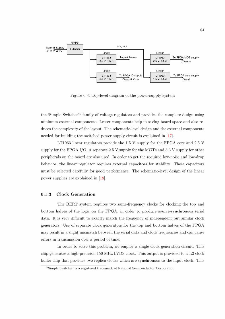
84
Figure 6.3: Top-level diagram of the power-supply system
the ‘Simple Switcher’1 family of voltage regulators and provides the complete design using
minimum external components. Lesser components help in saving board space and also re-
duces the complexity of the layout. The schematic-level design and the external components
needed for building the switched power supply circuit is explained in [17].
LT1963 linear regulators provide the 1.5 V supply for the FPGA core and 2.5 V
supply for the FPGA I/O. A separate 2.5 V supply for the MGTs and 3.3 V supply for other
peripherals on the board are also used. In order to get the required low-noise and low-drop
behavior, the linear regulator requires external capacitors for stability. These capacitors
must be selected carefully for good performance. The schematic-level design of the linear
power supplies are explained in [18].
6.1.3 Clock Generation
The BERT system requires two same-frequency clocks for clocking the top and
bottom halves of the logic on the FPGA, in order to produce source-synchronous serial
data. It is very difficult to exactly match the frequency of independent but similar clock
generators. Use of separate clock generators for the top and bottom halves of the FPGA
may result in a slight mismatch between the serial data and clock frequencies and can cause
errors in transmission over a period of time.
In order to solve this problem, we employ a single clock generation circuit. This
chip generates a high-precision 150 MHz LVDS clock. This output is provided to a 1:2 clock
buffer chip that provides two replica clocks which are synchronous to the input clock. This1‘Simple Switcher’ is a registered trademark of National Semiconductor Corporation

85
Figure 6.4: Block diagram of the clock generation system
ensures that both the halves of the logic on the FPGA will receive a clock of the exact same
frequency. The block diagram of the clock generation system is shown in Figure 6.4. The
clock signals are routed to the FPGA and terminated by on-chip LVDS termination.
6.2 Power Distribution System
The design of the PDS (Power Distribution System) is one of the most important
task in designing FPGA-based systems. Other large ICs such as microprocessors or custom
ASICs come with specific bypass capacitor requirements. Since FPGAs can be configured
to implement a variety of different designs at various frequencies, the power supply demands
fluctuate depending upon the application. Hence, a unique PDS design is required for each
FPGA-based system. Transient current demands are the main cause of ground-bounce in
high-speed systems. The power supply decoupling network must be tailored very closely to
these transient current needs, otherwise ground bounce and power supply noise will exceed
the limits of the device. Since the exact transient current behavior cannot be predicted, a
conservative design is adopted for the bypass capacitors.
The purpose of PDS is to provide power to all the devices in the system. Xilinx
FPGAs have a requirement that all supplies must not fluctuate more than 5% above or
5% below their nominal Vcc value. The power consumed by the FPGA varies over time
as a result of switching events inside the device. This can occur on the time scale from
nanoseconds to couple of seconds. The PDS must accommodate these variances in current
with as little change in power supply voltage as possible. The two major components of
any PDS are the voltage regulator and the decoupling capacitors. The voltage regulator
observes the output voltage and adjusts the current accordingly to keep the output voltage
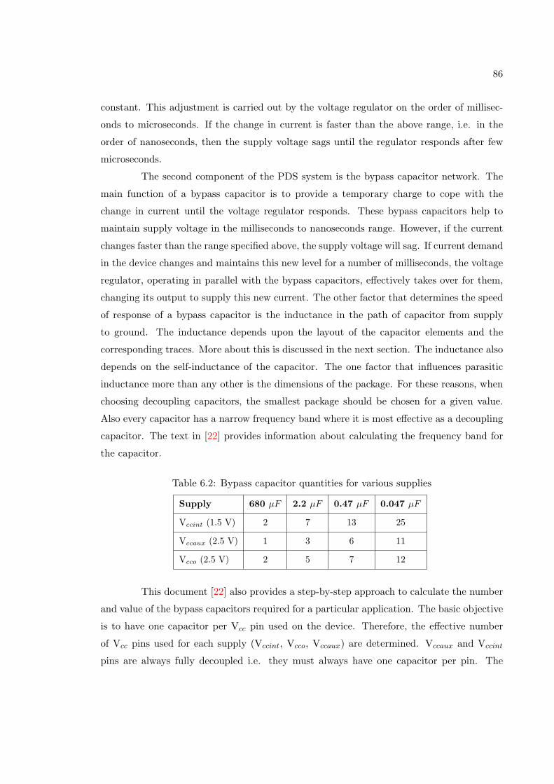
86
constant. This adjustment is carried out by the voltage regulator on the order of millisec-
onds to microseconds. If the change in current is faster than the above range, i.e. in the
order of nanoseconds, then the supply voltage sags until the regulator responds after few
microseconds.
The second component of the PDS system is the bypass capacitor network. The
main function of a bypass capacitor is to provide a temporary charge to cope with the
change in current until the voltage regulator responds. These bypass capacitors help to
maintain supply voltage in the milliseconds to nanoseconds range. However, if the current
changes faster than the range specified above, the supply voltage will sag. If current demand
in the device changes and maintains this new level for a number of milliseconds, the voltage
regulator, operating in parallel with the bypass capacitors, effectively takes over for them,
changing its output to supply this new current. The other factor that determines the speed
of response of a bypass capacitor is the inductance in the path of capacitor from supply
to ground. The inductance depends upon the layout of the capacitor elements and the
corresponding traces. More about this is discussed in the next section. The inductance also
depends on the self-inductance of the capacitor. The one factor that influences parasitic
inductance more than any other is the dimensions of the package. For these reasons, when
choosing decoupling capacitors, the smallest package should be chosen for a given value.
Also every capacitor has a narrow frequency band where it is most effective as a decoupling
capacitor. The text in [22] provides information about calculating the frequency band for
the capacitor.
Table 6.2: Bypass capacitor quantities for various supplies
Supply 680 µF 2.2 µF 0.47 µF 0.047 µF
Vccint (1.5 V) 2 7 13 25
Vccaux (2.5 V) 1 3 6 11
Vcco (2.5 V) 2 5 7 12
This document [22] also provides a step-by-step approach to calculate the number
and value of the bypass capacitors required for a particular application. The basic objective
is to have one capacitor per Vcc pin used on the device. Therefore, the effective number
of Vcc pins used for each supply (Vccint, Vcco, Vccaux) are determined. Vccaux and Vccint
pins are always fully decoupled i.e. they must always have one capacitor per pin. The
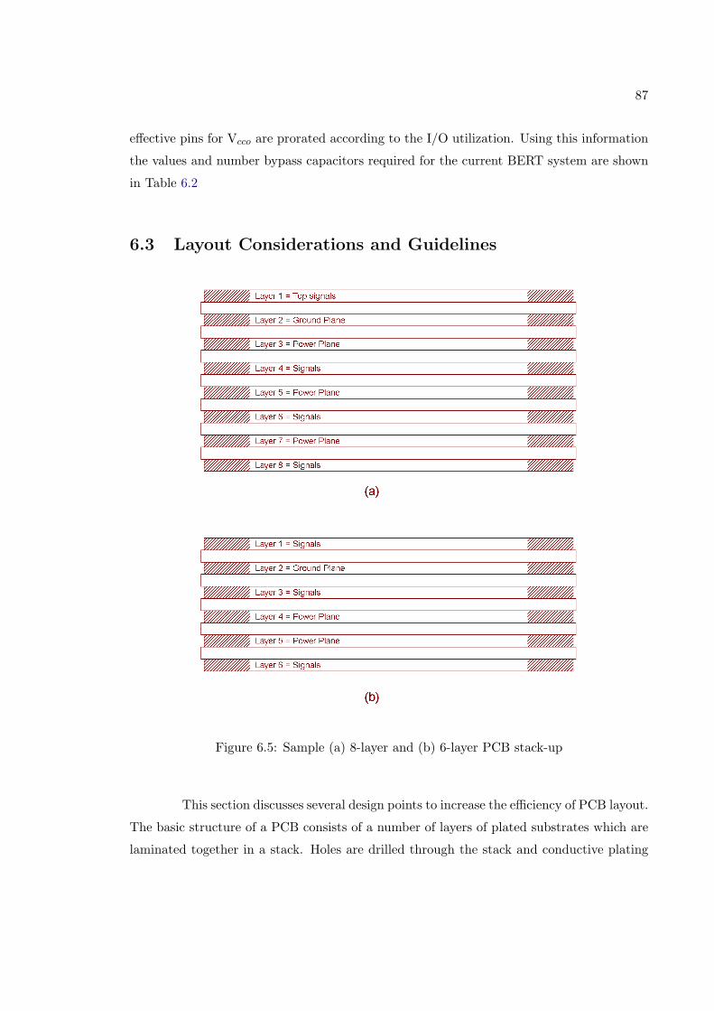
87
effective pins for Vcco are prorated according to the I/O utilization. Using this information
the values and number bypass capacitors required for the current BERT system are shown
in Table 6.2
6.3 Layout Considerations and Guidelines
Figure 6.5: Sample (a) 8-layer and (b) 6-layer PCB stack-up
This section discusses several design points to increase the efficiency of PCB layout.
The basic structure of a PCB consists of a number of layers of plated substrates which are
laminated together in a stack. Holes are drilled through the stack and conductive plating
88
is applied to these holes, selectively forming conductive connections, also known as Plated
Through Hole vias, between different layers. The first step in starting a PCB layout is to
determine the number of layers to be used. This also includes the decision about the PCB
stack-up i.e. deciding the signal and power/ground layers. Figure 6.5 shows two sample
PCB stack-up for the BERT system.
A single-ended signal trace along with the reference plane forms a transmission
line. For a differential trace, the transmission line is formed by combination of the two
traces and a reference plane. For ensuring good signal integrity on the board, transmission
lines must have controlled impedance and all signal traces must be properly terminated.
The characteristic impedance is determined by the geometry of the traces and the dielectric
constant of the material in the space around the signal trace. Every signal on the PCB has
a return path, which generally passes through a reference plane. Better signal integrity is
achieved by preventing breaks in return paths by providing a dedicated ground plane above
or below the signal trace. Various components on the board should be placed as close to
one another as possible, reducing the trace lengths. Intelligent placement avoids too much
bending of the PCB traces and use of vias when going from one component to the another.
Figure 6.6: Suggested layout for BGA package (Courtesy: Xilinx Inc)
Xilinx FPGAs come in a fine-pitch BGA package with a 1.0 mm ball pitch. Spe-

89
cial rules are needed to be followed for successful and effective routing of these packages on
PCBs. Xilinx provides guidelines for the dimensions of the land pads for the BGA balls and
their respective vias. Figure 6.6 denotes the important dimensions for them. The values
are:
- Solder Land Diameter (L) - 0.45 mm
- Opening in Solder Mask Diameter (M) - 0.55 mm
- Solder Ball Land Pitch (e) - 1 mm
- Line Width Between Via and Land (w) - 0.13 mm
- Distance between Via and Land (D) - 0.70 mm
- Via Land Diameter (VL) - 0.61 mm
- Through Hole Diameter (VH) - 0.30 mm
The BERT design also incorporates five RocketIO transceivers. The balls that
make up these channels are grouped within two outer rows of the top and bottom edges.
This makes it easy for the critical traces to escape and pair with their differential counterpart
easily. Figure 6.7 shows the layout of such traces.
Figure 6.7: Suggested dimensions for the traces (Courtesy: Xilinx Inc)
As discussed earlier, the inductance of a current path through the bypass capacitor

90
is proportional to the area of the loop that the current traverses. It is important to minimize
the size of this loop. The loop consists of the path through one power plane, up through
one via, through the connecting trace to the land, through the capacitor, through the other
land and connecting trace, down through the other via, and into the other plane, as shown
in Figure 6.8. By shortening the connecting traces, the area of this loop is minimized and
the inductance is reduced. Similarly, by reducing the via length through which the current
flows, loop area is minimized and inductance is reduced.
Figure 6.8: Mounting of the bypass capacitors (Courtesy: Xilinx Inc)
The above mentioned guidelines must be followed in order to make the layout
process simple and efficient. The data about the minimum dimensions of the traces, drill
sizes for the vias etc. should also be decided initially with the manufacturers. Another
important step before proceeding with PCB design, is to verify the availability of the com-
ponents with their respective suppliers. This avoids the need for a part replacement during
later stages of PCB design and hence saves a lot of time. Since the BERT system will be
used for a space experiment, radiation and other physical tests have to be performed to
ensure correct working of the system in space.

91
Chapter 7
Conclusions
We have demonstrated the design and implementation of a self-contained system
capable of performing BER testing and interfacing to an RS232 host. The current system
exhibits key advantages for the applications listed below.
1. This system provides a low cost alternative for manufacturing quality test systems.
2. The small form factor of the test system provides maximum portability.
3. The current design can be easily modified or extended to build test platforms for a
multitude of high-speed interconnect systems.
4. This test system together with a high-speed sampling oscilloscope provides a cost-
effective solution for academic and small scale research groups to perform accurate
BER testing and jitter measurements.
The BERT system can be interfaced to the SPA system via the RS232 interface
with minimal changes to the software code. FPGA based systems are faster to design and
hence are ideal for ORS payloads. The system can be used in an asynchronous configuration
where an external pattern generator is used to transmit data patterns and the BER tests are
performed on this system. Although the hardware-based stand alone BER testing systems
continue to be the best choice for BER testing, the proposed system proves a ideal solution
for certain specific applications.

92
7.1 Future Work
The BERT design is currently demonstrated on a general purpose FPGA devel-
opment board. The future work includes the development of a board customized for the
current application. The customized board will be evaluated on basis of the power consump-
tion and the integrity of transmitted waveforms. The BERT logic modules are capable of
running at almost double the current frequency of operation, but are restricted by the max-
imum speed that is supported by the RocketIOs. Newer FPGAs include RocketIOs capable
of transmitting at the data rates of up to 10.125 Gb/s. The current design can be ported to
these FPGAs for improved performance. Since the system will be used on-board a low-orbit
satellite, radiation testing needs to be performed. Certain changes in the logic modules such
as automatic powerdown of the unused BERT channels and PRBS generators can be made
to increase power efficiency.
93
Bibliography
[1] General requirements for instrumentation for performance measurements on digital
transmission equipment. ITU-T Recommendation O. 150, pages 3–6, May 1996.
[2] ATIS Telecom Glossary 2000. Alliance for Telecommunications Industry Solutions,
February 2000.
[3] Statistical Confidence Levels for Estimating BER Probability, Application Note 1095.
Maxim Integrated Products, October 2000.
[4] LFSRs as Functional Blocks in Wireless Applications, Application Note XAPP220.
Xilinx Incorporation, January 2001.
[5] Linear Feedback Shift Register in Virtex Devices, Application Note XAPP210. Xilinx
Incorporation, January 2001.
[6] Palani Subbiah. Bit-Error Rate (BER) For High-Speed Serial Data Communication.
Cypress Semiconductor, Data-communications Division, 2001.
[7] BER measurements reveal network health. Test & Measurement World, July 2002.
[8] Board Routability Guidelines with Xilinx Fine-Pitch BGA Packages. Xilinx Incorpo-
ration, November 2002.
[9] The UltraController Solution: A Lightweight PowerPC Microcontroller, Application
Note XAPP672. Xilinx Incorporation, September 2003.
[10] Virtex-II Pro RocketIO. Multi-Gigabit Transceiver Characterization Summary. Xilinx
Incorporation, 2003.
94
[11] Data2BRAM, Application Note. Xilinx Incorporation, August 2004.
[12] Major Kendall K. Brown. A Concept of Operations and Technology Implications for
Operationally Responsive Space. Air & Space Power Chronicles, June 2004.
[13] Mixed Signal ISP Flash MCU Family, Datasheet. Silicon Laboratories, December 2004.
[14] PowerPC 405 Processor Block Reference Guide, UG018. Xilinx Incorporation, August
2004.
[15] RocketIOTM Transceiver User Guide. Xilinx Incorporation, December 2004.
[16] 1.25/2.5/5.0 Gbps Quad Multi-rate Backplane Transceiver, Datasheet. National Semi-
conductor, March 2005.
[17] LM2678 SIMPLE SWITCHER High Efficiency 5A Step-Down Voltage Regulator. Na-
tional Semiconductor, April 2005.
[18] LT1963A Series 1.5A, Low Noise, Fast Transient Response LDO Regulators. Linear
Technologies, 2005.
[19] MP1763C/MP1764C/MP1764D Pulse Pattern Generator/Error Detector. Anritsu
Corporation, Atsugi-shi, Kanagawa, Japan, June 2005.
[20] OPB UART Lite (v1.00b), Product Specification DS422. Xilinx Incorporation, May
2005.
[21] Platform Studio User Guide. Xilinx Incorporation, February 2005.
[22] Power Distribution System (PDS) Design: Using Bypass/Decoupling Capacitors. Xil-
inx Incorporation, February 2005.
[23] Interconnects. International Technology Roadmap For Semiconductors, pages 46–50,
2005 Edition.
[24] SPA-U Applique Sensor Interface Module. Air Force Research Laboratory, June 2005,
Revision 2.
[25] Agilent J-BERT N4903A High-Performance Serial BERT with complete jitter tolerance
testing. Agilent Technologies, Palo Alto, California, January 2006.

95
[26] Achintya Halder and Abhijit Chatterjeer. Low-cost Production Test of BER for Wire-
less Receivers. May 2005.
[27] E.A. Newcombe, and S. Pasupathy. Error Rate Monitoring for Digital Communications.
volume 70, pages 805–825. IEEE Radio Frequency Integrated Circuits Symposium, Au-
gust 1982.
[28] Jian Xu, John Wilson, Stephen Mick, Lei Luo and Paul Franzon. 2.8Gb/s Inductively
Coupled Interconnect for 3-D ICs. VLSI Symposium, Japan, June 2005.
[29] Jim Lyke, Don Fronterhouse, Scott Cannon, Denise Lanza, Wheaton (Tony) Byers.
Space Plug-And-Play Avionics. AIAA 3rd Responsive Space Conference, 2005.
[30] John Wilson, Stephen Mick, Jian Xu, Lei Luo, Salvatore Bonafede, Alan Huffman,
Richard LaBennett and Paul Franzon. Fully Integrated AC Coupled Interconnect using
Buried Bumps. pages 11–14. Electrical Performance of Electronic Packaging, October
2005.
[31] L. Luo, J. M. Wilson, S. E. Mick, J. Xu, L. Zhang and P. D. Franzon. A 3Gb/s
AC Coupled Chip-to-Chip Communication using a Low Swing Pulse Receiver. pages
522–523. ISSCC Dig. Tech. Papers, February 2005.
[32] Lei Luo, John Wilson, Jian Xu, Stephen Mick and Paul Franzon. Signal Integrity
and Robustness of ACCI packaged systems. pages 11–14. Electrical Performance of
Electronic Packaging, October 2005.
[33] Marcel A. Kossel and Martin L. Schmatz. Jitter measurements of high-speed serial
links. volume 21, pages 536 – 543. IEEE Design & Test of Computers, Nov-Dec 2004.
[34] Stephen Mick. Analysis and Design Considerations for AC Coupled Interconnection
Systems. PhD thesis, NC State University, 2004.
[35] P. Palacharla, J. Chrostowski, R. Neumann and R. J. Gallenberger. Techniques for
Accelerated Measurement of Low Bit Error Rates in Computer Data Links. July 1995.
[36] Rammohan Malasani, Christian Bourde, and German Gutierrez. A SiGe 10-Gb/s
Multi-Pattern Bit Error Rate Tester. pages 321–324. IEEE Radio Frequency Integrated
Circuits Symposium, March 2003.

96
[37] Stephen Mick, John Wilson, and Paul Franzon. 4 Gbps High-Density AC Coupled In-
terconnection. pages 133–140. IEEE Custom Integrated Circuits Conference, February
2002.
[38] Stephen Mick, Lei Luo, John Wilson, and Paul Franzon. Buried Bump and AC Coupled
Interconnection Technology. volume 27. IEEE Transactions on Advanced Packaging,
February 2004.