DESIGN OF A 100W POWER AMPLIFIER WITH ...eie.uonbi.ac.ke/sites/default/files/cae/engineering/eie...i...
61
i UNIVERSITY OF NAIROBI FACULTY OF ENGINEERING DEPARTMENT OF ELECTRICAL AND INFORMATION ENGINEERING DESIGN OF A 100W POWER AMPLIFIER WITH DARLINGTON COMPLEMENTARY SYMMETRY OUTPUT POWER TRANSISTOR PROJECT INDEX: 113 SUBMITTED BY: KOLL JACKSON RISONA F17/37338/2010 SUPERVISOR: MR. S. L OGABA EXAMINER: PROF ABUNGU PROJECT SUBMITTED IN PARTIAL FULFILLMENT OF THE REQUIREMENT FOR THE AWARD OF THE DEGREE OF BACHELOR OF SCIENCE IN ELECTRICAL AND ELECTRONIC ENGINEERING OF THE UNIVERSITY OF NAIROBI 2016
Transcript of DESIGN OF A 100W POWER AMPLIFIER WITH ...eie.uonbi.ac.ke/sites/default/files/cae/engineering/eie...i...
i
UNIVERSITY OF NAIROBI
FACULTY OF ENGINEERING
DEPARTMENT OF ELECTRICAL AND INFORMATION ENGINEERING
DESIGN OF A 100W POWER AMPLIFIER WITH DARLINGTON
COMPLEMENTARY SYMMETRY OUTPUT POWER TRANSISTOR
PROJECT INDEX: 113
SUBMITTED BY: KOLL JACKSON RISONA
F17/37338/2010
SUPERVISOR: MR. S. L OGABA
EXAMINER: PROF ABUNGU
PROJECT SUBMITTED IN PARTIAL FULFILLMENT OF THE
REQUIREMENT FOR THE AWARD OF THE DEGREE OF
BACHELOR OF SCIENCE IN ELECTRICAL AND ELECTRONIC ENGINEERING
OF THE UNIVERSITY OF NAIROBI
2016
ii
DECLARATION OF ORIGINALITY
I, KOLL JACKSON RISONA (F17/37338/2010), hereby declare that this project is my
original work. To the best of my knowledge, the work presented here has not been presented
for a degree in any other Institution of Higher Learning.
………………………………………… …………………
Name of student Date
This project has been submitted for examination with my approval as university supervisor.
………………………………………… …………………
Name of supervisor Date

iii
DEDICATION
I dedicate this project to my parents Mr. and Mrs. John Kol ole Sawi, my siblings and friends
for their continued and undying support throughout this journey and I am forever grateful for
the opportunity they have given me to achieve my dreams.

iv
ACKNOWLEDGEMENT
I would like to express my gratitude towards my project supervisor Mr. S.L. Ogaba of The
Nairobi University and my colleagues for their guidance and constant supervision as well as
providing necessary information regarding the project and also for their support in
completing the project.
I am also grateful to electronics lab technicians for giving me permission to use their
facilities.
v
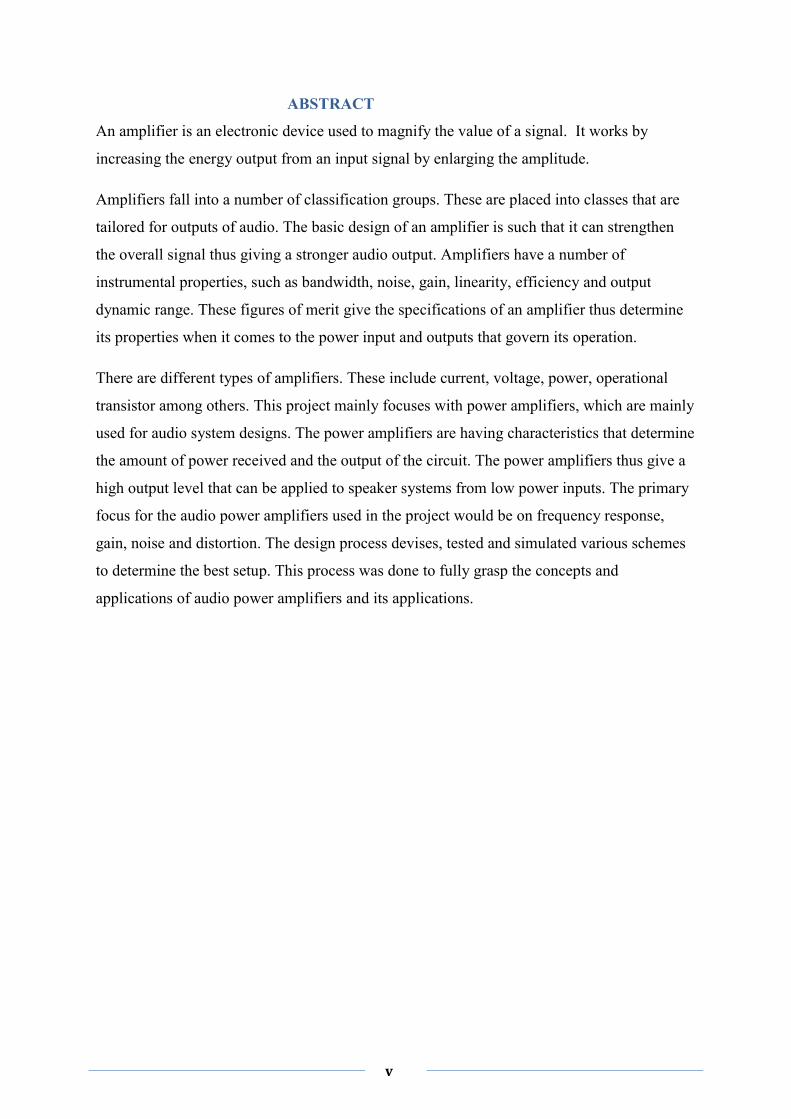
ABSTRACT
An amplifier is an electronic device used to magnify the value of a signal. It works by
increasing the energy output from an input signal by enlarging the amplitude.
Amplifiers fall into a number of classification groups. These are placed into classes that are
tailored for outputs of audio. The basic design of an amplifier is such that it can strengthen
the overall signal thus giving a stronger audio output. Amplifiers have a number of
instrumental properties, such as bandwidth, noise, gain, linearity, efficiency and output
dynamic range. These figures of merit give the specifications of an amplifier thus determine
its properties when it comes to the power input and outputs that govern its operation.
There are different types of amplifiers. These include current, voltage, power, operational
transistor among others. This project mainly focuses with power amplifiers, which are mainly
used for audio system designs. The power amplifiers are having characteristics that determine
the amount of power received and the output of the circuit. The power amplifiers thus give a
high output level that can be applied to speaker systems from low power inputs. The primary
focus for the audio power amplifiers used in the project would be on frequency response,
gain, noise and distortion. The design process devises, tested and simulated various schemes
to determine the best setup. This process was done to fully grasp the concepts and
applications of audio power amplifiers and its applications.

vi
Table of Contents
Contents
DECLARATION OF ORIGINALITY ................................................................................................... ii
DEDICATION ....................................................................................................................................... iii
ACKNOWLEDGEMENT ..................................................................................................................... iv
ABSTRACT ............................................................................................................................................ v
Table of Contents ................................................................................................................................... vi
LIST OF TABLES ................................................................................................................................. ix
LIST OF FIGURES ................................................................................................................................ x
ABBREVIATIONS ............................................................................................................................... xi
CHAPTER 1: INTRODUCTION ........................................................................................................... 1
Power Amplifier.................................................................................................................................. 1
Problem statement ............................................................................................................................... 1
Significance......................................................................................................................................... 1
Project objective.................................................................................................................................. 2
Scope ................................................................................................................................................... 2
CHAPTER 2: LITERATURE REVIEW ................................................................................................ 3
AMPLIFIERS ..................................................................................................................................... 3
Amplifier Gain ................................................................................................................................ 3
Input Resistance .............................................................................................................................. 4
Output Resistance ........................................................................................................................... 5
POWER AMPLIFIER ........................................................................................................................ 5
POWER OUTPUT TRANSISTORS .................................................................................................. 9
DARLINGTON COMPLEMENTARY ......................................................................................... 9
AUDIO CROSSOVER NETWORK ................................................................................................ 10
PASSIVE FILTERS .......................................................................................................................... 11
ACTIVE FILTERS ........................................................................................................................... 11
Types of Active Filters ...................................................................................................................... 12
Butterworth Filter: ........................................................................................................................ 13
Chebyshev Filter. .......................................................................................................................... 13
Bessel Filter .................................................................................................................................. 14
Elliptic Filter ................................................................................................................................. 14
SWITCHED-CAPACITOR FILTER ........................................................................................... 15

vii
CHAPTER 3: DESIGN ......................................................................................................................... 16
POWER AMPLIFIER ...................................................................................................................... 16
Darlington Output Stage ................................................................................................................... 17
Voltage Amplification stage ............................................................................................................. 20
Driver Transistor ........................................................................................................................... 20
Bias Spreader ................................................................................................................................ 21
INPUT STAGE ................................................................................................................................. 22
Short Circuit Protector ...................................................................................................................... 24
ACTIVE FILTER ............................................................................................................................. 25
Sallen-Key Topology .................................................................................................................... 25
Power Supply .................................................................................................................................... 29
CIRCUIT COMPONENTS .............................................................................................................. 31
Resistors ........................................................................................................................................ 31
Diodes ........................................................................................................................................... 32
Capacitors ..................................................................................................................................... 32
Transistors ..................................................................................................................................... 33
Heat sinks ...................................................................................................................................... 33
POWER AMPLIFIER PERFORMANCE SPECIFICATION.......................................................... 34
Distortion ...................................................................................................................................... 34
Clipping......................................................................................................................................... 34
Frequency response ....................................................................................................................... 35
Output Current .............................................................................................................................. 35
Rated Output Power ...................................................................................................................... 35
Slew rate........................................................................................................................................ 36
CHAPTER 4: RESULTS AND SIMULATIONS ................................................................................ 36
Circuit Diagram ................................................................................................................................ 36
Circuit Calculations .......................................................................................................................... 37
Computer Simulation Results ........................................................................................................... 38
Results ............................................................................................................................................... 39
Simulation ..................................................................................................................................... 39
Laboratory Implementation........................................................................................................... 39
FILTER DESIGN SIMULATION RESULTS ............................................................................. 40
LOW-PASS FILTER .................................................................................................................... 41
BAND-PASS FILTER .................................................................................................................. 41
viii
HIGH-PASS FILTER ................................................................................................................... 42
3-WAY FILTER FREQUENCY RESPONSE ............................................................................. 43
CHAPTER 5 ................................................................................................................................. 45
5.1 DISCUSSION ............................................................................................................................. 45
5.2 CONCLUSION ........................................................................................................................... 45
5.3 RECOMMENDATION .............................................................................................................. 47
REFERENCES ..................................................................................................................................... 48
APPENDICES ...................................................................................................................................... 49

ix
LIST OF TABLES
Table 2 current source results ............................................................................................................... 22
Table 3 Resistor color bands ................................................................................................................. 31
Table 4 Power Amplifier simulation results ......................................................................................... 39
Table 5 Output Power simulation ......................................................................................................... 39
Table 6 Laboratory results .................................................................................................................... 39
Table 7POWER AMPLIFIER FREQUENCY RESPONSE ................................................................. 40
Table 8 Low Pass Filter ........................................................................................................................ 41
Table 9 Low Pass Filter ........................................................................................................................ 41
Table 10 Band Pass Filter ..................................................................................................................... 42
Table 11 High Pass Filter Freuency Response ...................................................................................... 43

x
LIST OF FIGURES
Figure 1 Amplifier Gain .......................................................................................................................... 3
Figure 2 Class A Amplifier ..................................................................................................................... 7
Figure 3 Class B amplifier Waveforms................................................................................................... 8
Figure 4 Darlington Complementary .................................................................................................... 10
Figure 5 Frequency Response curve ..................................................................................................... 12
Figure 6 Chebyshev and Butterworth frequency response ................................................................... 13
Figure 7 Bessel Filter frequency response ............................................................................................ 14
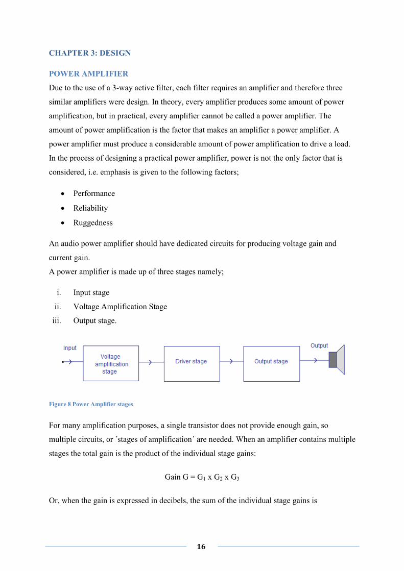
Figure 8 Power Amplifier stages .......................................................................................................... 16
Figure 9 Darlington Complementary Output Stage .............................................................................. 18
Figure 10 VAS stage ............................................................................................................................. 20
Figure 11 Current Source ...................................................................................................................... 21
Figure 12 Input Stage ............................................................................................................................ 23
Figure 13 Short Circuit Protector .......................................................................................................... 25
Figure 14 Low Pass Filter ..................................................................................................................... 26
Figure 15 High Pass Filter .................................................................................................................... 27
Figure 16 Band Pass Filter .................................................................................................................... 28
Figure 17 Power Supply ........................................................................................................................ 30
Figure 18 Characteristic curve .............................................................................................................. 32
Figure 19 Power Amplifier Frequency response ................................................................................. 35
Figure 20 100w Power Amplifier ......................................................................................................... 36
Figure 21 Amplifier Simulated Waveform ........................................................................................... 39
Figure 22 Laboratory Waveform .......................................................................................................... 40
Figure 23 Band Pass Filter Frequency Response .................................................................................. 42
Figure 24 High Pass Filter Freuency Response .................................................................................... 43
Figure 25 3-way Active filter frequency response ................................................................................ 44
Figure 26 circuit PCB layout ................................................................................................................ 49
Figure 27 Circuit Design ....................................................................................................................... 50
xi
ABBREVIATIONS
Hz= Hertz
dB = Decibel
KHz =Kilo Hertz
µ = micro
m = milli
H = Henries
F = Farads
Ω = Ohms
Π = 3.14
R = Resistance
L= Inductance
C = Capacitance
Zo= Impedance
fc = Cross over frequency/ Cut off frequency
V= Voltage
P = Power
f = frequency
LPF = Low pass filter
HPF = High pass filter
BPF = Band pass filter
FL= Lower cut off frequency
FH = Upper cut off frequency
W= Watts
Rms = root mean square.

1
CHAPTER 1: INTRODUCTION
Power Amplifier
An amplifier, electronic amplifier or amp is an electronic device that can increase the power
of a signal. It amplifies an audio signal with low power so that it can be used to drive a
loudspeaker. Power amplifiers are required for applications where high current switching
currents are needed, such as driving a motor or feed a loudspeaker. As they are called, power
amplifiers are used to deliver power to the load.
Amplifiers are used in wireless communications and broadcasting, and in audio equipment of
all kinds. They are categorized as either weak-signal amplifiers or power amplifiers.
The first audio power amplifier was made in 1906 by Lee De Forest and came in the form of
the triode vacuum tube. This particular mechanism evolved from the Audion, which was
developed by De Forest. Unlike the triode which had three elements, the Audion only had
two and did not amplify sound. Later on during the same year, the triode, a device with the
capability of adjusting the movement of electrons from a filament to a plate and thus
modulating sound was invented. It was vital in the invention of the first AM radio. Since
then, the advancement in the electronics industry has seen numerous improvements of
amplifier designs such as the invention of vacuum tubes after the world war two and the
invention of silicon transistors in the 1970’s which replaced almost all amplifiers because
they were smaller and thus more efficient while also better at reducing distortion levels and
cheaper to make.
Problem statement
The best amplifier systems effectively produce the required amplification without damage to
the loudspeaker being driven by it and also they are able to operate in the whole frequency
range audible to the human ear. Most modern music systems have separate speakers (woofer,
mid-range & tweeter) connected to output of amplifiers. This project is employs the design of
a power amplifiers with a short circuit protection and three way active filter network.
Significance
With constant evolution in technologically, power amplifiers have become more
sophisticated and small in size. They can also produce more power and better music quality
than previously designed power amplifiers. Improved technology has led to expensive power
2
amplifiers. This study is aimed at showing and providing alternative and affordable way of
having a high quality power amplifier through the design of a 100W power amplifier with a
3-way active filter to enable the amplifier cover the whole range of frequencies i.e., base,
tweeter and midrange. This is achieved by using locally available and affordable components
to achieve the same high quality audibility.
Project objective
The main objective in this project is to design and build a power amplifier that will amplify
signals up to 100 watts in the range of 20Hz to 20 kHz. This will be achieved by
i. Choosing a cheaper and less bulky circuitry that can produce frequencies in the
required range
ii. Design a power amplifier with a Darlington complementary output transistor
iii. To design a preamplifier that will help boost the signal to level required for input
signal of the power amplifier
iv. To design an active filter that will enable a 3way output for different signal
frequencies i.e., low pass, band pass and high pass
v. Test the complete power amplifier built and verify it works.
Scope
The project will entail building a power amplifier that could amplify sound signals to
frequencies suitable for human ear (around 20 kHz) with a total output power of 100 watts
divided into three outputs each of a different frequency. It will involve the hardware design of
a preamplifier, an active crossover filter to divide the frequencies and a power amplifier to
amplify the signal that will produce good musical signals in a 3way output to enhance and
make the sound signal for clear and undistorted.
CHAPTER 2: LITERATURE REVIEW
AMPLIFIERS
Amplifier circuits form the basis of most electronic systems many of which need t
high power to drive some output device. An amplifier is an electronic device that can increase
the power of a signal. It does this by taking energy from a power supply and controlling the
output to match the input signal shape but with the larger
amplifier modulates the output of the power supply. There are many forms of electronic
circuits classed as amplifiers, from Operational Amplifiers and Small Signal Amplifiers up to
Large Signal and Power Amplifiers with the cl
size of the signal, its configuration, class and application.
amplifiers have three main properties;
Input resistance (RIN)
Output resistance (ROUT
Amplifier gain (A)
With the above properties, all classes of amplifiers can be analyzed to show the relationship
between these properties.
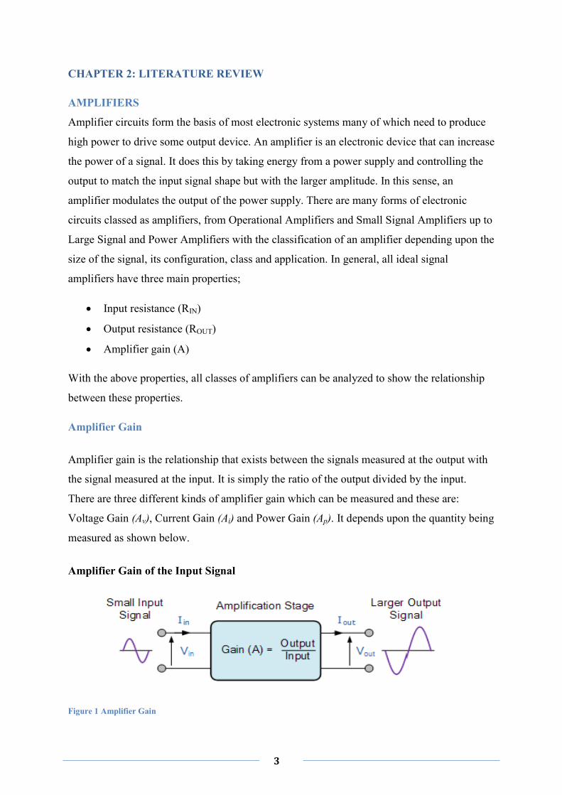
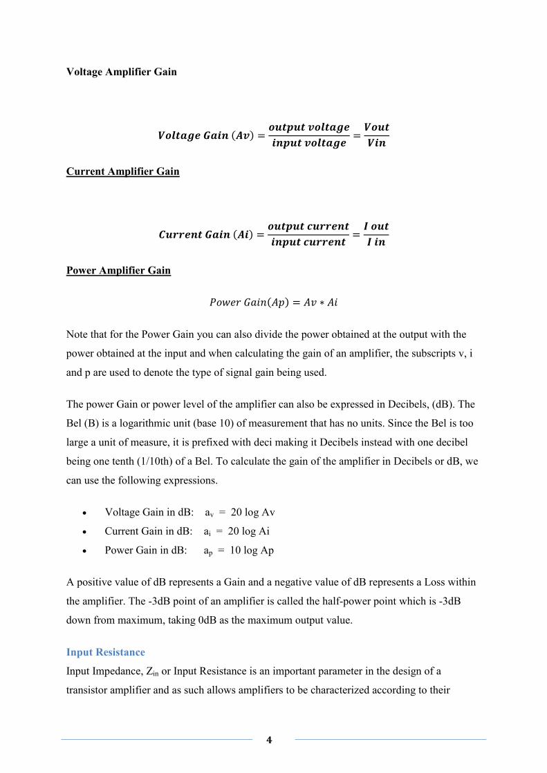
Amplifier Gain
Amplifier gain is the relationship that exists between the signals measured at the output with
the signal measured at the input.
There are three different kinds of amplifier gain which can be measured and these are:
Voltage Gain (Av), Current Gain
measured as shown below.
Amplifier Gain of the Input Signal
Figure 1 Amplifier Gain
3
CHAPTER 2: LITERATURE REVIEW
Amplifier circuits form the basis of most electronic systems many of which need t
high power to drive some output device. An amplifier is an electronic device that can increase
It does this by taking energy from a power supply and controlling the
output to match the input signal shape but with the larger amplitude. In this sense, an
amplifier modulates the output of the power supply. There are many forms of electronic
circuits classed as amplifiers, from Operational Amplifiers and Small Signal Amplifiers up to
Large Signal and Power Amplifiers with the classification of an amplifier depending upon the
size of the signal, its configuration, class and application. In general, all ideal signal
have three main properties;
OUT)
ove properties, all classes of amplifiers can be analyzed to show the relationship
Amplifier gain is the relationship that exists between the signals measured at the output with
the signal measured at the input. It is simply the ratio of the output divided by the input.
There are three different kinds of amplifier gain which can be measured and these are:
Current Gain (Ai) and Power Gain (Ap). It depends upon the quantity being
Amplifier Gain of the Input Signal
Amplifier circuits form the basis of most electronic systems many of which need to produce
high power to drive some output device. An amplifier is an electronic device that can increase
It does this by taking energy from a power supply and controlling the
amplitude. In this sense, an
amplifier modulates the output of the power supply. There are many forms of electronic
circuits classed as amplifiers, from Operational Amplifiers and Small Signal Amplifiers up to
assification of an amplifier depending upon the
general, all ideal signal
ove properties, all classes of amplifiers can be analyzed to show the relationship
Amplifier gain is the relationship that exists between the signals measured at the output with
is simply the ratio of the output divided by the input.
There are three different kinds of amplifier gain which can be measured and these are:
. It depends upon the quantity being
4
Voltage Amplifier Gain
() =
=
Current Amplifier Gain
() =
=
Power Amplifier Gain
() = ∗
Note that for the Power Gain you can also divide the power obtained at the output with the
power obtained at the input and when calculating the gain of an amplifier, the subscripts v, i
and p are used to denote the type of signal gain being used.
The power Gain or power level of the amplifier can also be expressed in Decibels, (dB). The
Bel (B) is a logarithmic unit (base 10) of measurement that has no units. Since the Bel is too
large a unit of measure, it is prefixed with deci making it Decibels instead with one decibel
being one tenth (1/10th) of a Bel. To calculate the gain of the amplifier in Decibels or dB, we
can use the following expressions.
Voltage Gain in dB: av = 20 log Av
Current Gain in dB: ai = 20 log Ai
Power Gain in dB: ap = 10 log Ap
A positive value of dB represents a Gain and a negative value of dB represents a Loss within
the amplifier. The -3dB point of an amplifier is called the half-power point which is -3dB
down from maximum, taking 0dB as the maximum output value.
Input Resistance
Input Impedance, Zin or Input Resistance is an important parameter in the design of a
transistor amplifier and as such allows amplifiers to be characterized according to their
5
effective input and output impedances as well as their power and current ratings. An
amplifiers impedance value is particularly important for analysis especially when cascading
individual amplifier stages together one after another to minimize distortion of the signal.
The input impedance of an amplifier is the input impedance seen by the source driving the
input of the amplifier. If it is too low, it can have an adverse loading effect on the previous
stage and possibly affecting the frequency response and output signal level of that stage. But
in most applications, common emitter and common collector amplifier circuits generally have
high input impedances.
Some types of Amplifier Designs, such as the common collector amplifier circuit
automatically have high input impedance and low output impedance by the very nature of
their design. Amplifiers can have high input impedance, low output impedance, and virtually
any arbitrary gain, but where amplifiers input impedance is lower than desired, the output
impedance of the previous stage can be adjusted to compensate or if this is not possible then
buffer amplifier stages may be needed.
Output Resistance
Every electricity supplying component has output impedance and so does power amplifiers.
You could look at it as a resistor in series with the output of the amplifier, representing the
imperfection of that amplifiers output stage. The output impedance is related to the damping
factor. Damping factor is the measure for the control an amplifier has over a speaker cabinet.
A high damping factor coincides with low output impedance which is good for the power
amplifier. Damping factor is calculated as follows;
=
This shows why it is important for loudspeaker cables should be made of large diameter
copper wires to ensure the damping factor is not lowered.
POWER AMPLIFIER
This is an amplifier which produces amplification of power between the input and output. It
is an electronic amplifier that amplifies low-power signals composed primarily of frequencies
between 20 and 20,000 Hz, which is the human range of hearing, to a level suitable for

6
driving loudspeakers. Power amplifiers are required for applications where high current
switching currents are needed, such as driving a motor or feed a loudspeaker. As they are
called, power amplifiers are used to deliver power to the load and as we know power is the
product of current and voltage. Therefore, the power delivered to the load is the product of
voltage and current supplied. In a practical amplifier, there are several stages that amplify a
weak signal until sufficient power is available to operate a loudspeaker or other output
devices. The first stages perform the function of power amplification and only the last stage is
designed to provide maximum power. The final stage is known as the power stage. A power
amplifier does not amplify power but it actually draws power from DC supply connected to
the output circuit and converts it into AC signal power useful for the load of the power
amplifier. This conversion from DC power supply input to the AC voltage signal output
forms the basic principle of the power amplifier thus a power amplifier may also be defined
as a device that converts DC power to AC signal power. This AC power at the output is
controlled by the input signal. Although the amplification is high, the efficiency of the
conversion is poor.
= ℎ
=
CLASSIFICATION OF POWER AMPLIFIERS
Audio power Amplifiers
They are known as small signal power amplifiers and they raise the power levels of signals
that have audio-frequency range i.e., 20Hz up to 20 kHz.
Radio-power amplifiers
Also known as large signal power amplifiers and they raise the power level of signals that
have radio frequency range. They amplify a specific frequency or narrow band of frequencies
while rejecting all other frequencies.
CLASSIFICATION ACCORDING TO MODE OF OPERATION
The classification is based on the amount of transistor bias and amplitude of the input signal.
CLASS A POWER AMPLIFIER
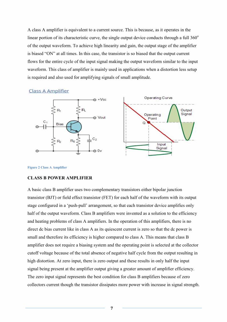
A class A amplifier is equivalent to a current source. This is because, as it operates in the
linear portion of its characteristic curve, the single output device conducts through a full 360
of the output waveform. To achieve high linearity and gain, the output stage of the amplifier
is biased “ON” at all times. In this case, the transistor is so biased that the o
flows for the entire cycle of the input signal making the output waveform similar to the input
waveform. This class of amplifier is
is required and also used for amplifying signals of s
Figure 2 Class A Amplifier
CLASS B POWER AMPLIFIER
A basic class B amplifier uses two complementary transistors either bipolar junction
transistor (BJT) or field effect transistor (FET) for each half of the wavefo
stage configured in a ‘push-pull
half of the output waveform. Class B amplifiers were invented as a solution to the efficiency
and heating problems of class A amplifiers. In
direct dc bias current like in class A as its quiescent current is zero so that
small and therefore its efficiency is higher compared to class A. This means that class B
amplifier does not require a biasing system and the operating point is selected at the collector
cutoff voltage because of the total absence of negative half cycle from the output resulting in
high distortion. At zero input, there is
signal being present at the amplifier output giving a greater amount of amplifier efficiency.
The zero input signal represents the best condition for class B amplifiers because of zero
collectors current though the transistor dissipates more power with
7
A class A amplifier is equivalent to a current source. This is because, as it operates in the
its characteristic curve, the single output device conducts through a full 360
the output waveform. To achieve high linearity and gain, the output stage of the amplifier
is biased “ON” at all times. In this case, the transistor is so biased that the o
flows for the entire cycle of the input signal making the output waveform similar to the input
This class of amplifier is mainly used in applications when a distortion less
is required and also used for amplifying signals of small amplitude.
CLASS B POWER AMPLIFIER
A basic class B amplifier uses two complementary transistors either bipolar junction
(BJT) or field effect transistor (FET) for each half of the waveform with its output
pull’ arrangement, so that each transistor device amplifies only
half of the output waveform. Class B amplifiers were invented as a solution to the efficiency
and heating problems of class A amplifiers. In the operation of this amplifiers, there is no
direct dc bias current like in class A as its quiescent current is zero so that the dc power is
small and therefore its efficiency is higher compared to class A. This means that class B
a biasing system and the operating point is selected at the collector
cutoff voltage because of the total absence of negative half cycle from the output resulting in
high distortion. At zero input, there is zero output and these results in only half the in
signal being present at the amplifier output giving a greater amount of amplifier efficiency.
The zero input signal represents the best condition for class B amplifiers because of zero
current though the transistor dissipates more power with increase in signal strength.
A class A amplifier is equivalent to a current source. This is because, as it operates in the
its characteristic curve, the single output device conducts through a full 360o
the output waveform. To achieve high linearity and gain, the output stage of the amplifier
is biased “ON” at all times. In this case, the transistor is so biased that the output current
flows for the entire cycle of the input signal making the output waveform similar to the input
distortion less setup
A basic class B amplifier uses two complementary transistors either bipolar junction
rm with its output
arrangement, so that each transistor device amplifies only
half of the output waveform. Class B amplifiers were invented as a solution to the efficiency
amplifiers, there is no
the dc power is
small and therefore its efficiency is higher compared to class A. This means that class B
a biasing system and the operating point is selected at the collector
cutoff voltage because of the total absence of negative half cycle from the output resulting in
in only half the input
signal being present at the amplifier output giving a greater amount of amplifier efficiency.
The zero input signal represents the best condition for class B amplifiers because of zero
increase in signal strength.
Figure 3 Class B amplifier Waveforms
ADVANTAGES OF CLASS B POWER AMPLIFIER
Have high amplifier efficiency
Compared to class A, they experience less power dissipation
They can be used for more powerfu
For ideal cases, they have no DC components in the output for ideal cases
DISADVANTAGES OF CLASS B AMPLIFERS
Creates crossover distortion
Supply current changes with signal, hence it requires stabilized supply
CLASS AB POWER AMPLIFIERS
Class AB combines the good points of class A and class B amplifiers. This class of amplifiers
is probably the most common amplifier class currently used in home stereo because of their
improved efficiency brought about by class B advantages an
closer to that of a Class A amplifier.
base current level of class B power amplifiers and above one
class A; this bias condition is
to achieve a full output cycle, but the dc bias level is usually closer to zero base current level
for better power efficiency. For class AB operation the output signal swing occurs between
180 degree and 360 degree and is neither class A nor class B operation.
8
Class B amplifier Waveforms
ADVANTAGES OF CLASS B POWER AMPLIFIER
Have high amplifier efficiency
Compared to class A, they experience less power dissipation
They can be used for more powerful outputs compared to class A
For ideal cases, they have no DC components in the output for ideal cases
DISADVANTAGES OF CLASS B AMPLIFERS
Creates crossover distortion
Supply current changes with signal, hence it requires stabilized supply
AMPLIFIERS
Class AB combines the good points of class A and class B amplifiers. This class of amplifiers
is probably the most common amplifier class currently used in home stereo because of their
improved efficiency brought about by class B advantages and a distortion performance that is
closer to that of a Class A amplifier. An amplifier may be biased at a dc level above the zero
base current level of class B power amplifiers and above one-half the supply voltage level of
class A; this bias condition is class AB. Class AB operation still needs a push
to achieve a full output cycle, but the dc bias level is usually closer to zero base current level
for better power efficiency. For class AB operation the output signal swing occurs between
0 degree and 360 degree and is neither class A nor class B operation.
For ideal cases, they have no DC components in the output for ideal cases
Supply current changes with signal, hence it requires stabilized supply
Class AB combines the good points of class A and class B amplifiers. This class of amplifiers
is probably the most common amplifier class currently used in home stereo because of their
d a distortion performance that is
An amplifier may be biased at a dc level above the zero
half the supply voltage level of
class AB. Class AB operation still needs a push-pull connection
to achieve a full output cycle, but the dc bias level is usually closer to zero base current level
for better power efficiency. For class AB operation the output signal swing occurs between
9
POWER OUTPUT TRANSISTORS
There are many reasons that designers need very high gain transistors, and although they are
available in a single package, it is generally better to build your own using discrete devices.
This gives much greater flexibility, and allows you to create configurations that are optimised
for the specific task required.
In many power amplifiers the op-amp circuit is constructed with discrete components
specifically designed for higher rail Voltages. To create a high gain transistor, it is a matter of
connecting two or more transistors such that the collector current of the first is amplified by
the second. Output transistors are added to provide extra current to drive a speaker. Large
output transistors only have a small HFE current gain; therefore driver transistors are placed
in front of the output transistors to increase the total current gain. The bias string can now be
placed in the Class A driver circuit. Output transistors can be arranged in three different
ways;
Darlington Complementary
Quasi Complementary
Compound Complementary
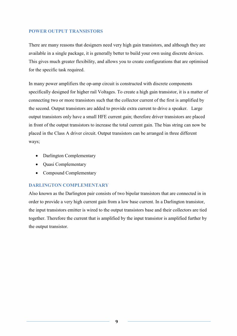
DARLINGTON COMPLEMENTARY
Also known as the Darlington pair consists of two bipolar transistors that are connected in in
order to provide a very high current gain from a low base current. In a Darlington transistor,
the input transistors emitter is wired to the output transistors base and their collectors are tied
together. Therefore the current that is amplified by the input transistor is amplified further by
the output transistor.
Figure 4 Darlington Complementary
APPLICATIONS OF DARLINGTON TRANSISTORS
They are used in applications where a high gain is
Darlington are used in light sensitive
Power regulators
Audio amplifier output stage
Display drivers
ADVANTAGES OF DARLINGTON PAIR
Have very high current gain
Have very high input impedance for the overall circuit
Darlington pairs are widely available in a single package
easy circuit configuration to use
DISADVANTAGES OF THE DARLINGTON PAIR
They have slow switching speeds
Have limited bandwidth
Higher overall base-emitter voltage of 2V
High saturation voltage which can lead to high levels of power dissipation
AUDIO CROSSOVER NETWORK
Almost all individual loudspeaker drivers cannot cover the entire audio spectrum from low
frequencies to high frequencies with acceptable relative volume and lack of distortion hence
most hi-fi speaker systems use a combination of several loudspeaker drivers for each
10
APPLICATIONS OF DARLINGTON TRANSISTORS
They are used in applications where a high gain is needed at a low frequency while
sensitive circuits. Some applications include:
Audio amplifier output stage
Motor controllers
Touch and light sensors
Solenoid control
ADVANTAGES OF DARLINGTON PAIR
Have very high current gain
nput impedance for the overall circuit
Darlington pairs are widely available in a single package hence offer a convenient and
easy circuit configuration to use
DISADVANTAGES OF THE DARLINGTON PAIR
They have slow switching speeds
Have limited bandwidth
emitter voltage of 2Vbe
High saturation voltage which can lead to high levels of power dissipation
AUDIO CROSSOVER NETWORK
Almost all individual loudspeaker drivers cannot cover the entire audio spectrum from low
cies with acceptable relative volume and lack of distortion hence
fi speaker systems use a combination of several loudspeaker drivers for each
needed at a low frequency while photo-
Motor controllers
Touch and light sensors
Solenoid control
hence offer a convenient and
High saturation voltage which can lead to high levels of power dissipation
Almost all individual loudspeaker drivers cannot cover the entire audio spectrum from low
cies with acceptable relative volume and lack of distortion hence
fi speaker systems use a combination of several loudspeaker drivers for each
11
frequency band. With optimized loudspeakers for each band, crossover networks split the
audio signal into separate frequency bands that can be separately routed to the optimized
loudspeaker using filters.
Classifications of crossovers;
Passive filters and active filters
Analog and digital
Discrete time and continuous time
Linear and non-linear
Infinite impulse response (IIR) and finite impulse response (FIT)
High pass, low pass, band pass, band reject, and all pass
PASSIVE FILTERS
This type of filter is made entirely of passive components. It is commonly arranged in a cauer
topology to obtain a Butterworth filter. Passive implementations of linear filters are based on
combinations of resistors (R) with reactive components such as inductors (L) and capacitors
(C).In its network, capacitors allow high frequency signals and block low-frequency signals
while inductors block high frequency signals and conduct low-frequency signals. A filter in
which a signal passes through a capacitor provides a path to ground or in which signal passes
through an inductor, presents less attenuation to low-frequency signals than high frequency
signals and is therefore a low-pass filter. On the other hand, a high-pass filter, occurs if a
signal passes through a capacitor or has a path to ground through an inductor, enabling the
filter to present less attenuation to high-frequency signals then low-frequency signals.
Although resistors on their own have no frequency selective properties, they are used in
circuits with inductors and capacitors to determine time-constants circuits and the frequencies
to which they respond.
Very high performance active filter networks are likely to be more cheaper than passive filter
networks due to individual components capable of good performance at high currents and
voltages at which speaker systems driven are hard to make. Passive filter networks do not
depend upon an external power supply.
ACTIVE FILTERS
These are usually amplifying elements, mostly op-amps, with resistors and capacitors in their
feedback loops meant to synthesize the desired filter characteristics. The active filters can

have high-input impedance, low output impedance and virtually any amount of gain.
are easier to design than passive filters because they do not have inductors hence inductor
effects and problems associated with them are reduced. Accuracy and value spacing are some
of the problems but they also affect capacitors at a lesser degree compared to inductors.
high frequencies, performance
elements but within the range of the amplifiers’ operating frequency.
By use low tolerance resistors and capacitors, the op
accuracy at the amplifiers’ operating frequency range but due to the amplifying circuitry,
active filters will generate noise which can be minimized by the use of lo
and careful circuit design.
There are basically 4 types of active
Butterworth,
Chebyshev,
Bessel and
Elliptic filters.
Types of Active Filters
Butterworth, Chebyshev, Bessel and Elliptic filters.
Figure 5 Frequency Response curve
12
t impedance, low output impedance and virtually any amount of gain.
are easier to design than passive filters because they do not have inductors hence inductor
effects and problems associated with them are reduced. Accuracy and value spacing are some
of the problems but they also affect capacitors at a lesser degree compared to inductors.
high frequencies, performance is hindered by the gain bandwidth product of the amplifying
elements but within the range of the amplifiers’ operating frequency.
use low tolerance resistors and capacitors, the op-amp active filter can achieve very good
accuracy at the amplifiers’ operating frequency range but due to the amplifying circuitry,
active filters will generate noise which can be minimized by the use of low
There are basically 4 types of active filters. They are;
Butterworth, Chebyshev, Bessel and Elliptic filters.
t impedance, low output impedance and virtually any amount of gain. They
are easier to design than passive filters because they do not have inductors hence inductor
effects and problems associated with them are reduced. Accuracy and value spacing are some
of the problems but they also affect capacitors at a lesser degree compared to inductors. At
is hindered by the gain bandwidth product of the amplifying
amp active filter can achieve very good
accuracy at the amplifiers’ operating frequency range but due to the amplifying circuitry,
w-noise amplifiers

Butterworth Filter:
This filter is also called as maximally flat filter.
filter well in the pass band. Frequency response
in figure. The Butterworth filter has an essentially flat amplitude
the cut-off frequency. The sharpness of the cut
that all the three filters reach a roll
than cut-off. Although Butterworth filters achieve the sharpest attenuation, their phase
as a function of frequency is non
cut-off region and a maximally
The Butterworth filter has characteristic somewhere be
filters. It has a moderate roll-off of the skirt and a slightly non
Figure 6 Chebyshev and Butterworth frequency response
Chebyshev Filter.
It is also called a equal ripple filter
pass band. Both Butterworth and Chebyshev filters exhibit large
frequency. A drawback of the Chebyshev fil
below the cut-off frequency. This gain ripple, ex
filter design.
13
This filter is also called as maximally flat filter. This class of filters approximates the ideal
filter well in the pass band. Frequency response curves of different types of filters are shown
in figure. The Butterworth filter has an essentially flat amplitude-frequency response up
off frequency. The sharpness of the cut-off can be seen in the figure. It is to be noted
reach a roll-off slope of -40 dB per decade at frequencies much larger
off. Although Butterworth filters achieve the sharpest attenuation, their phase
as a function of frequency is non-linear. It has a monotonic drop in gain with frequency in the
off region and a maximally flat response below cut-off frequency, as il
Butterworth filter has characteristic somewhere between those of Chebyshev and Bessel
off of the skirt and a slightly nonlinear phase responses.
Chebyshev and Butterworth frequency response
ple filter. It gives a sharper cut-off than Butterworth filter in the
. Both Butterworth and Chebyshev filters exhibit large phase shifts near the cut
frequency. A drawback of the Chebyshev filter is the appearance of gain maxima and minima
off frequency. This gain ripple, expressed in db, is an adjustable parameter in
This class of filters approximates the ideal
curves of different types of filters are shown
quency response up to
off can be seen in the figure. It is to be noted
decade at frequencies much larger
off. Although Butterworth filters achieve the sharpest attenuation, their phase-shift
linear. It has a monotonic drop in gain with frequency in the
off frequency, as illustrated in figure.
tween those of Chebyshev and Bessel
linear phase responses.
off than Butterworth filter in the
phase shifts near the cut-off
ter is the appearance of gain maxima and minima
pressed in db, is an adjustable parameter in
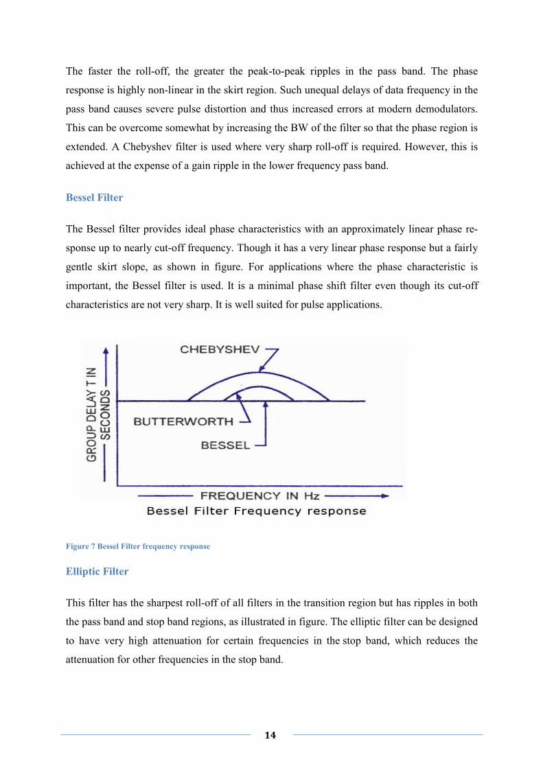
The faster the roll-off, the greater the peak
response is highly non-linear in the skirt region. Such unequal delays of data frequency in the
pass band causes severe pulse distor
This can be overcome somewhat by increasing the BW of the filter so that the phase region is
extended. A Chebyshev filter is used where very sharp roll
achieved at the expense of a gain ripple in the lower frequency pass
Bessel Filter
The Bessel filter provides ideal phase characteristics with an approximately linear phase re
sponse up to nearly cut-off frequency. Though it has a very linear phase response but a fairly
gentle skirt slope, as shown in figure. For applic
important, the Bessel filter is used. It is a minimal phase shift filter even though its cut
characteristics are not very sharp. It is well suited for pulse applica
Figure 7 Bessel Filter frequency response
Elliptic Filter
This filter has the sharpest roll
the pass band and stop band regions, as illustrated in figure. The
to have very high attenuation for certain frequencies in the
attenuation for other frequencies in the stop band.
14
the greater the peak-to-peak ripples in the pass
linear in the skirt region. Such unequal delays of data frequency in the
band causes severe pulse distortion and thus increased errors at modern demodulators.
what by increasing the BW of the filter so that the phase region is
A Chebyshev filter is used where very sharp roll-off is required. However, this is
achieved at the expense of a gain ripple in the lower frequency pass band.
The Bessel filter provides ideal phase characteristics with an approximately linear phase re
off frequency. Though it has a very linear phase response but a fairly
gentle skirt slope, as shown in figure. For applications where the phase characteristic is
important, the Bessel filter is used. It is a minimal phase shift filter even though its cut
characteristics are not very sharp. It is well suited for pulse applications.
sel Filter frequency response
This filter has the sharpest roll-off of all filters in the transition region but has ripples in both
the pass band and stop band regions, as illustrated in figure. The elliptic filter can be designed
ery high attenuation for certain frequencies in the stop band, which reduces the
attenuation for other frequencies in the stop band.
peak ripples in the pass band. The phase
linear in the skirt region. Such unequal delays of data frequency in the
tion and thus increased errors at modern demodulators.
what by increasing the BW of the filter so that the phase region is
off is required. However, this is
The Bessel filter provides ideal phase characteristics with an approximately linear phase re-
off frequency. Though it has a very linear phase response but a fairly
ations where the phase characteristic is
important, the Bessel filter is used. It is a minimal phase shift filter even though its cut-off
but has ripples in both
elliptic filter can be designed
stop band, which reduces the

15
SWITCHED-CAPACITOR FILTER
This type of filter is widely available in monolithic form. The switched-capacitor filter solves
some of the problems found in standard active filters and also increases the capabilities of
filters. It needs no external capacitor or inductors and this filter is set to a typical accuracy of
+ or – 0.2% by an external clock frequency. Through changing the clock frequency, the cut-
off frequencies of consistent, repeatable filter designs to be variable over a wide range and in
addition, the switched capacitor filters can have low sensitivity to temperature changes. This
type of filter is clocked and its input signal is sampled at a high rate then processed on a
discrete-time instead of continuous-time like the conventional active and passive filers.
Switched-Capacitor filters contain MOS switches and on-chip capacitors are closely matched
to other capacitors on the IC hence integrated filters whose cutoff frequencies are
proportional to, and determined only by external clock frequency
Advantages of switched-capacitor filter
They can achieve high dynamic range since the signal does not require quantization
They can be easily implemented on an integrated circuit
They occupy a small chip area
Their frequency characteristics can be changed easily by changing the clock speed
Disadvantages of switched-capacitor filters
They produce more noise at the output
They need a clock circuit and anti-aliasing filters
They are not suited for high frequencies
They experience sample data effect
CHAPTER 3: DESIGN
POWER AMPLIFIER
Due to the use of a 3-way active filter, each filter requires an amplifier and therefore three
similar amplifiers were design.
amplification, but in practical, every
amount of power amplification is the factor that makes an amplifier a power amp
power amplifier must produce a considerable amount of power amplification to drive a load.
In the process of designing a prac
considered, i.e. emphasis is given to the following factors;
Performance
Reliability
Ruggedness
An audio power amplifier should have dedicated circuits for producing voltage gain and
current gain.
A power amplifier is made up of three stages namely;
i. Input stage
ii. Voltage Amplification Stage
iii. Output stage.
Figure 8 Power Amplifier stages
For many amplification purposes, a single transistor does not provide enough gain, so
multiple circuits, or ´stages of amplification´ are needed. When an amplifier contains multiple
stages the total gain is the product of the individual stage gains:
Or, when the gain is expressed in decibels, the sum of the individual stage gains is
16
way active filter, each filter requires an amplifier and therefore three
imilar amplifiers were design. In theory, every amplifier produces some amount of power
practical, every amplifier cannot be called a power amplifier. The
amount of power amplification is the factor that makes an amplifier a power amp
power amplifier must produce a considerable amount of power amplification to drive a load.
In the process of designing a practical power amplifier, power is not the only factor that is
considered, i.e. emphasis is given to the following factors;
An audio power amplifier should have dedicated circuits for producing voltage gain and
A power amplifier is made up of three stages namely;
Voltage Amplification Stage
For many amplification purposes, a single transistor does not provide enough gain, so
multiple circuits, or ´stages of amplification´ are needed. When an amplifier contains multiple
he product of the individual stage gains:
Gain G = G1 x G2 x G3
Or, when the gain is expressed in decibels, the sum of the individual stage gains is
way active filter, each filter requires an amplifier and therefore three
amplifier produces some amount of power
amplifier. The
amount of power amplification is the factor that makes an amplifier a power amplifier. A
power amplifier must produce a considerable amount of power amplification to drive a load.
tical power amplifier, power is not the only factor that is
An audio power amplifier should have dedicated circuits for producing voltage gain and
For many amplification purposes, a single transistor does not provide enough gain, so
multiple circuits, or ´stages of amplification´ are needed. When an amplifier contains multiple
Or, when the gain is expressed in decibels, the sum of the individual stage gains is
17
Total gain in dBs = dB1 + dB2 + dB3.
The way in which the individual stages are coupled together is important. The design of the
coupling circuitry must fulfil several requirements, including:
Impedance Matching.
Correct Frequency Response.
DC Isolation.
Output Transistor Matching
In the output stage transistors, the positive half-cycle and the negative half-cycle are
supposed to have same behavior otherwise an even-order distortion will result. The signal in
both the top and bottom transistors follows different paths depending on the direction of net
current flow to the load.
Beta Matching
The difference in transistor gain will result to difference between positive and negative going
signal. This difference in current gain of the upper and lower half of the output stage cause
the load on the driver stage to be different on the negative and positive half-cycles of the
signal current swing resulting second harmonic distortion.
Emitter and Base Resistance Matching
A base resistor provides the necessary resistance to bias the base junction of a bipolar junction
transistor (BJT). The resistor “Rb” controls the amount of current “Ib” flowing into the base, which
controls the amount of current flowing through the collector “Ic”. The value of this resistance is
different for different input voltages.
Darlington Output Stage
This is the stage connected to the loudspeaker. It consists of two emitter followers one after
the other. The output stage of a power amplifier produces a current gain that is a product of
the betas of the driver and output transistors. This stage also produces unity gain
approximately.
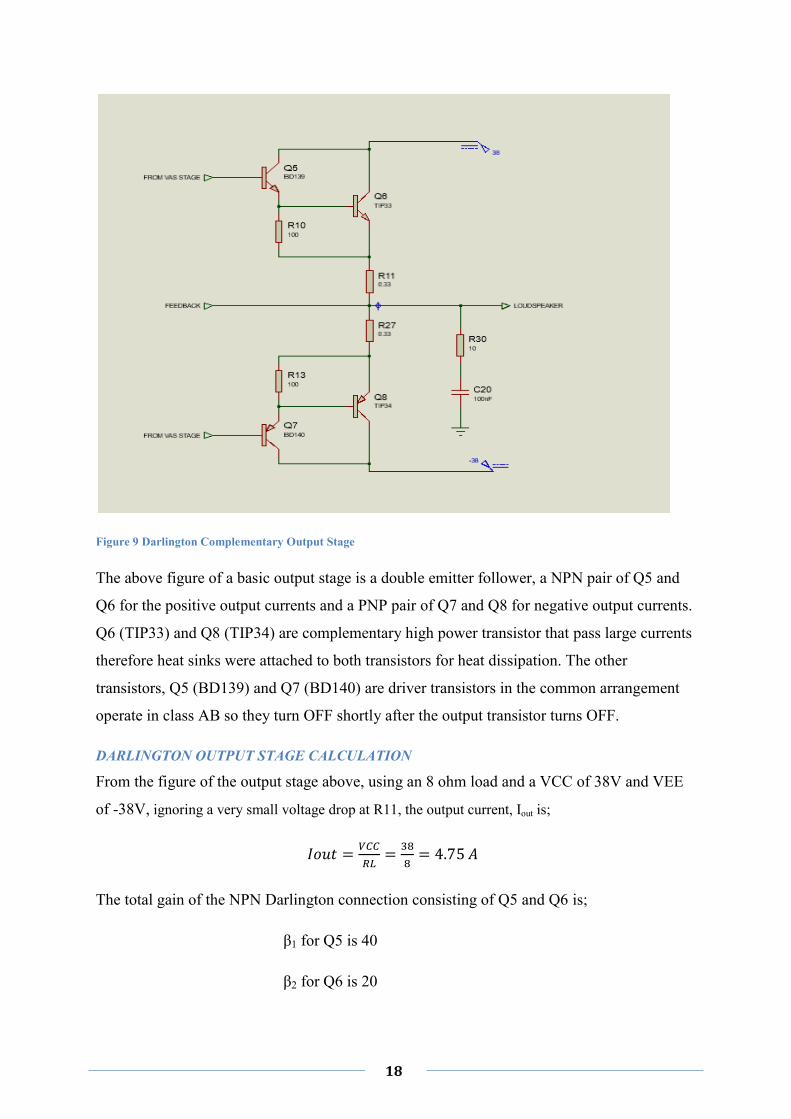
Figure 9 Darlington Complementary Output Stage
The above figure of a basic output stage is a double emitter follower, a NPN pair of Q5 and
Q6 for the positive output currents and a PNP pair of Q7 and Q8 for
Q6 (TIP33) and Q8 (TIP34) are complementary high power transistor that pass large currents
therefore heat sinks were attached to both transistors for heat dissipation. The other
transistors, Q5 (BD139) and Q7
operate in class AB so they turn OFF
DARLINGTON OUTPUT STAGE CALCULATION
From the figure of the output stage above, using an 8 ohm load and a VCC of 38V and VEE
of -38V, ignoring a very small voltage drop at R
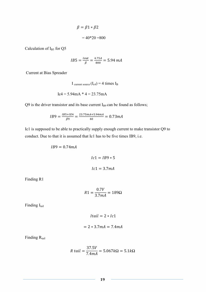
The total gain of the NPN Darlington connection consisting of Q5 and Q6 is;
β
β
18
Darlington Complementary Output Stage
The above figure of a basic output stage is a double emitter follower, a NPN pair of Q5 and
Q6 for the positive output currents and a PNP pair of Q7 and Q8 for negative output currents.
(TIP34) are complementary high power transistor that pass large currents
were attached to both transistors for heat dissipation. The other
and Q7 (BD140) are driver transistors in the common arrangement
ate in class AB so they turn OFF shortly after the output transistor turns OFF.
DARLINGTON OUTPUT STAGE CALCULATION
From the figure of the output stage above, using an 8 ohm load and a VCC of 38V and VEE
ignoring a very small voltage drop at R11, the output current, Iout is;
=
=
= 4.75
The total gain of the NPN Darlington connection consisting of Q5 and Q6 is;
β1 for Q5 is 40
β2 for Q6 is 20
The above figure of a basic output stage is a double emitter follower, a NPN pair of Q5 and
negative output currents.
(TIP34) are complementary high power transistor that pass large currents
were attached to both transistors for heat dissipation. The other
are driver transistors in the common arrangement
turns OFF.
From the figure of the output stage above, using an 8 ohm load and a VCC of 38V and VEE
The total gain of the NPN Darlington connection consisting of Q5 and Q6 is;
19
= 1 ∗ 2
= 40*20 =800
Calculation of IB5 for Q5
5 =
=
.
= 5.94
Current at Bias Spreader
I current source (Ic4) = 4 times IB
Ic4 = 5.94mA * 4 = 23.75mA
Q9 is the driver transistor and its base current IB9 can be found as follows;
9 =
=
..
= 0.73
Ic1 is supposed to be able to practically supply enough current to make transistor Q9 to
conduct. Due to that it is assumed that Ic1 has to be five times IB9, i.e.
9 = 0.74
1 = 9 ∗ 5
1 = 3.7
Finding R1
1 =0.7
3.7= 189Ω
Finding Itail
= 2 ∗ 1
= 2 ∗ 3.7 = 7.4
Finding Rtail
=37.5
7.4= 5.067Ω = 5.1Ω

Voltage Amplification stage
This stage provides all the voltage gain as i
Driver transistor,
A bias spreader and
A current source for boots strapping.
Figure 10 VAS stage
Driver Transistor
Most of the open loop voltage gain of the amplifier is provided by the trans
capacitor determines the dominant pole. The dominant pole is the pole which dominates the step
response of a system. This capacitor represents the miller
where the collector pole of transistor Q
that which exists as internal capacitance of Q9. The 47pF capacitor causes pole
playing a critical role in stabilizing the negative feedback loop around the amplifier.
20
Voltage Amplification stage
This stage provides all the voltage gain as its name suggests. It consists of a;
ent source for boots strapping.
Most of the open loop voltage gain of the amplifier is provided by the transistor
capacitor determines the dominant pole. The dominant pole is the pole which dominates the step
response of a system. This capacitor represents the miller-capacitor dominant-pole compensation
where the collector pole of transistor Q9 is lowered by adding external miller-capacitance, 47pF, to
that which exists as internal capacitance of Q9. The 47pF capacitor causes pole-splitting while also
playing a critical role in stabilizing the negative feedback loop around the amplifier.
Q9 while the 47pF
capacitor determines the dominant pole. The dominant pole is the pole which dominates the step
pole compensation
capacitance, 47pF, to
splitting while also
playing a critical role in stabilizing the negative feedback loop around the amplifier.
Bias Spreader
This stage is also known as a preset. It is used when a voltage drop equal to a multiple of Vbe drop is
needed. The required bias voltage for the output stage is developed across the bias spreader
usually a Vbe multiplier design around Q3.
The components R9, R12, VR1 and the transistor Q3 make up the bias spreader which controls the
quiescent current by setting it to minimum through adjusting the variable resistor VR1 we can adjust
level of idle current or the amount of bias voltage
protects the output transistors by balancing the current supplied to the upper and lower output
transistors.
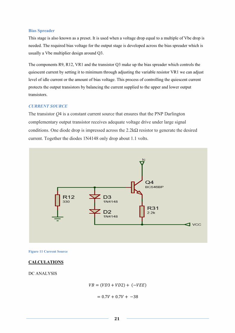
CURRENT SOURCE
The transistor Q4 is a constant current source that ensures that the PNP Darlington
complementary output transistor receives adequate voltage drive under large signal
conditions. One diode drop is impressed across the 2.2k
current. Together the diodes 1N4148 only drop about 1.1 volts.
Figure 11 Current Source
CALCULATIONS
DC ANALYSIS
21
This stage is also known as a preset. It is used when a voltage drop equal to a multiple of Vbe drop is
needed. The required bias voltage for the output stage is developed across the bias spreader
usually a Vbe multiplier design around Q3.
, VR1 and the transistor Q3 make up the bias spreader which controls the
quiescent current by setting it to minimum through adjusting the variable resistor VR1 we can adjust
or the amount of bias voltage. This process of controlling the quiescent current
protects the output transistors by balancing the current supplied to the upper and lower output
4 is a constant current source that ensures that the PNP Darlington
mplementary output transistor receives adequate voltage drive under large signal
. One diode drop is impressed across the 2.2kΩ resistor to generate the desired
current. Together the diodes 1N4148 only drop about 1.1 volts.
= (3 + 2) + (−)
= 0.7 + 0.7 + −38
This stage is also known as a preset. It is used when a voltage drop equal to a multiple of Vbe drop is
needed. The required bias voltage for the output stage is developed across the bias spreader which is
, VR1 and the transistor Q3 make up the bias spreader which controls the
quiescent current by setting it to minimum through adjusting the variable resistor VR1 we can adjust
process of controlling the quiescent current
protects the output transistors by balancing the current supplied to the upper and lower output
4 is a constant current source that ensures that the PNP Darlington
mplementary output transistor receives adequate voltage drive under large signal
resistor to generate the desired
22
= 1.4 − 38
= −36.6
= −
= −36.6 − 0.7
= −37.3
= − (−)
= −37.3 + 38
= 0.7
=
=
0.7
2.2Ω= 0.32
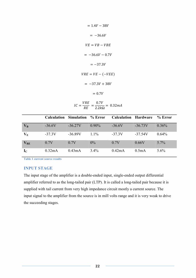
Calculation Simulation % Error Calculation Hardware % Error
VB -36.6V -36.27V 0.90% -36.6V -36.73V 0.36%
VE -37.3V -36.89V 1.1% -37.3V -37.54V 0.64%
VRE 0.7V 0.7V 0% 0.7V 0.66V 5.7%
IC 0.32mA 0.43mA 3.4% 0.42mA 0.5mA 5.6%
Table 1 current source results
INPUT STAGE
The input stage of the amplifier is a double-ended input, single-ended output differential
amplifier referred to as the long-tailed pair (LTP). It is called a long-tailed pair because it is
supplied with tail current from very high impedance circuit mostly a current source. The
input signal to the amplifier from the source is in mill volts range and it is very weak to drive
the succeeding stages.

Figure 12 Input Stage
The transistors Q1 and Q2 form the differential pair. This stage is usually characterized by a
fairly low voltage gain ranging from 1 to 15. The
used to implement a voltage divider which determines the feedback fraction of the output
signal to the input signal. These resistors
In dB, gain =20log10 8.79 = 18.88 dB
R3 (also known as Rtail) and the zener diode Z1, determine the total current in the differ
pair of Q1 and Q2. The resistor R5
feedback at DC. This in collaboration with the differential pair ensures that the output voltage
of the amplifier is zero when no signal is at the input.
23
Q2 form the differential pair. This stage is usually characterized by a
fairly low voltage gain ranging from 1 to 15. The resistors R5 and R6 are feedback resistors
used to implement a voltage divider which determines the feedback fraction of the output
These resistors set the AC voltage gain.
=6
5=
5.1Ω
580Ω= 8.79
8.79 = 18.88 dB
the zener diode Z1, determine the total current in the differ
resistor R5 in series with the capacitor C2 create a complete negative
feedback at DC. This in collaboration with the differential pair ensures that the output voltage
of the amplifier is zero when no signal is at the input.
Q2 form the differential pair. This stage is usually characterized by a
are feedback resistors
used to implement a voltage divider which determines the feedback fraction of the output
the zener diode Z1, determine the total current in the differential
in series with the capacitor C2 create a complete negative
feedback at DC. This in collaboration with the differential pair ensures that the output voltage
24
The current fed to the Voltage Amplification Stage is approximately 5 times less than the
current Ic1, that is, Ic1 is supposed to be able to practically supply enough current to make
transistor Q9 in the VAS stage to conduct. Due to that it is assumed that Ic1 has to be five
times IB9, i.e.
9 = 0.73
1 = 9 ∗ 5
1 = 3.7
Finding R1
1 =0.7
3.7= 189Ω
Finding Itail
= 2 ∗ 1
= 2 ∗ 3.7 = 7.4
Finding Rtail (R3)
=37.5
7.4= 5.067Ω = 5.1Ω
The input impedance was calculated and found to be ZIN= 150 kΩ
Short Circuit Protector
Short circuit protection involves monitoring the current in the output devices and restricting the drive
applied to the output stage whenever excessive current is detected. The following circuit was designed
as a short circuit protector;
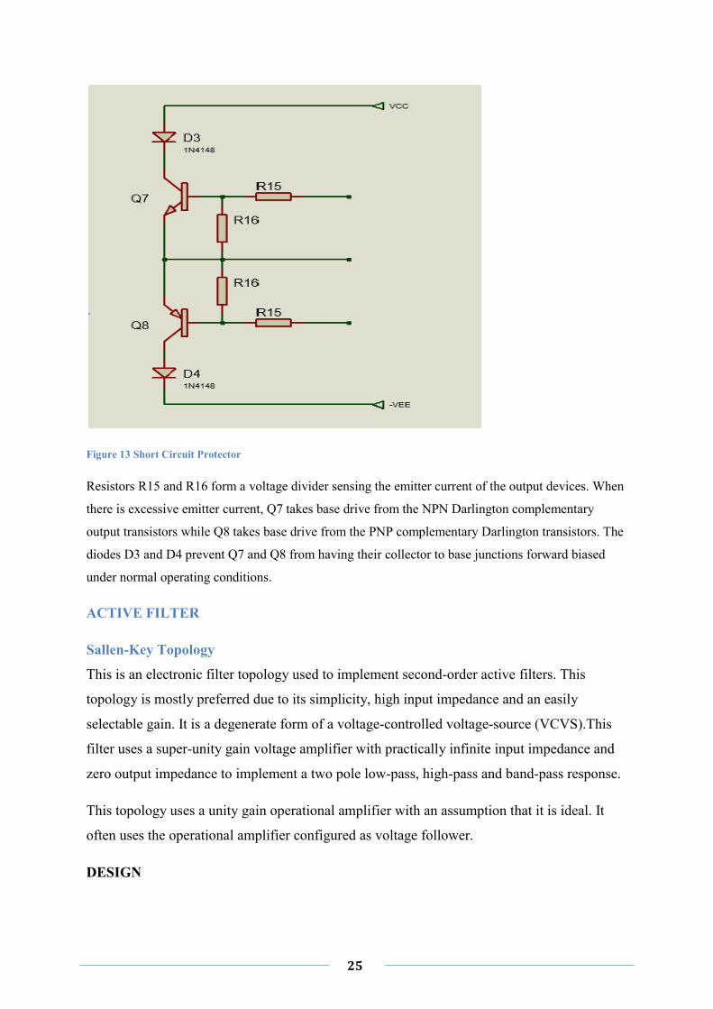
Figure 13 Short Circuit Protector
Resistors R15 and R16 form a voltage divider sensing the emitter current of the outpu
there is excessive emitter current
output transistors while Q8 takes base drive from the PNP complementary Darlington transistors. The
diodes D3 and D4 prevent Q7 and Q8 from having
under normal operating conditions.
ACTIVE FILTER
Sallen-Key Topology
This is an electronic filter topology used to implement second
topology is mostly preferred due to its simplic
selectable gain. It is a degenerate form of a voltage
filter uses a super-unity gain voltage amplifier with practically infinite input impedance
zero output impedance to impl
This topology uses a unity gain operational amplifier with an assumption that it is ideal. It
often uses the operational amplifier configured as voltage follower.
DESIGN
25
Resistors R15 and R16 form a voltage divider sensing the emitter current of the outpu
re is excessive emitter current, Q7 takes base drive from the NPN Darlington complementary
while Q8 takes base drive from the PNP complementary Darlington transistors. The
diodes D3 and D4 prevent Q7 and Q8 from having their collector to base junctions forward biased
under normal operating conditions.
This is an electronic filter topology used to implement second-order active filters. This
topology is mostly preferred due to its simplicity, high input impedance and an easily
selectable gain. It is a degenerate form of a voltage-controlled voltage-source (VCVS).This
unity gain voltage amplifier with practically infinite input impedance
zero output impedance to implement a two pole low-pass, high-pass and band
This topology uses a unity gain operational amplifier with an assumption that it is ideal. It
often uses the operational amplifier configured as voltage follower.
Resistors R15 and R16 form a voltage divider sensing the emitter current of the output devices. When
Darlington complementary
while Q8 takes base drive from the PNP complementary Darlington transistors. The
their collector to base junctions forward biased
order active filters. This
ity, high input impedance and an easily
source (VCVS).This
unity gain voltage amplifier with practically infinite input impedance and
pass and band-pass response.
This topology uses a unity gain operational amplifier with an assumption that it is ideal. It
26
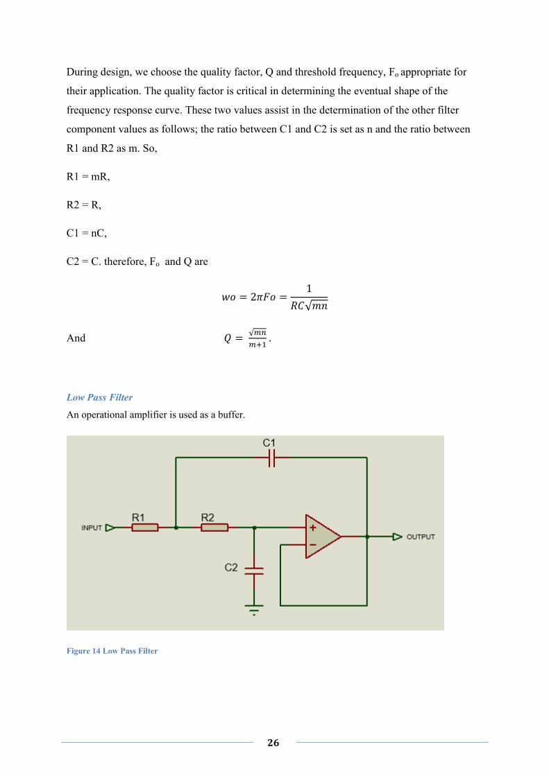
During design, we choose the quality factor, Q and threshold frequency, Fo appropriate for
their application. The quality factor is critical in determining the eventual shape of the
frequency response curve. These two values assist in the determination of the other filter
component values as follows; the ratio between C1 and C2 is set as n and the ratio between
R1 and R2 as m. So,
R1 = mR,
R2 = R,
C1 = nC,
C2 = C. therefore, Fo and Q are
= 2 =1
√
And = √
.
Low Pass Filter
An operational amplifier is used as a buffer.
Figure 14 Low Pass Filter
Taking Fo to be 1.2kHz and Q to be 0.5, we set R1 to be 12k
unknown parameters as follows;
= √
=
1 = 2
2
Therefore, C= 0.01µF through the ratios m and n, we get
R1=12kΩ, R2=12kΩ
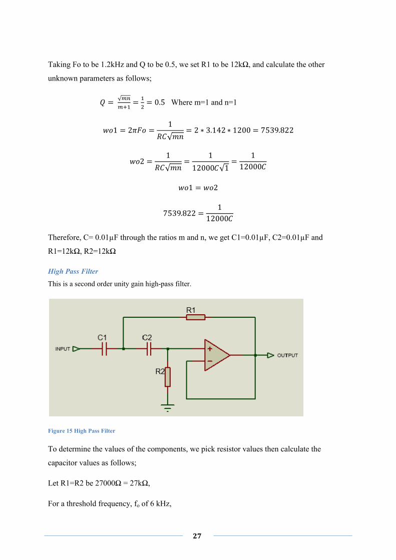
High Pass Filter
This is a second order unity gain high
Figure 15 High Pass Filter
To determine the values of the components, we pick resistor values then calculate the
capacitor values as follows;
Let R1=R2 be 27000Ω = 27kΩ,
For a threshold frequency, fo of 6 kHz,
27
Taking Fo to be 1.2kHz and Q to be 0.5, we set R1 to be 12kΩ, and calculate the other
unknown parameters as follows;
= 0.5 Where m=1 and n=1
=1
√= 2 ∗ 3.142 ∗ 1200 = 7539.822
2 =1
√=
1
12000√1=
1
12000
1 = 2
7539.822 =1
12000
Therefore, C= 0.01µF through the ratios m and n, we get C1=0.01µF, C2=0.01µF and
This is a second order unity gain high-pass filter.
To determine the values of the components, we pick resistor values then calculate the
Ω = 27kΩ,
of 6 kHz,
Ω, and calculate the other
822
C1=0.01µF, C2=0.01µF and
To determine the values of the components, we pick resistor values then calculate the

For R1=R2=R and C1=C2=C,
1 = 2
Band-pass Filter
A band-pass filter works to screen out frequencies that are too low or too high, giving ease passage
only to frequencies within a certain range.
Figure 16 Band Pass Filter
Where fo is the centre frequency
Where vo=output voltage
Vi = input voltage
= damping ratio = 1
28
=1
2√1 ∗ 2 ∗ 1 ∗ 2
For R1=R2=R and C1=C2=C, =
√∗
6000 =1
2√27000 ∗
2 = = 0.98 ∗ 10 = 1 0.001µ
pass filter works to screen out frequencies that are too low or too high, giving ease passage
only to frequencies within a certain range.
=1
2
1
3 ∗ 1 ∗ 2
1
2+
1
2
Where fo is the centre frequency = 3.5 kHz
=
2(2)
+ 2(2) + (2)
pass filter works to screen out frequencies that are too low or too high, giving ease passage
29
=1
2= 0.5
=3
1∗
−2
1 + 2= −1
Where K is the gain at center frequency, and Q is the quality factor.
Using the above equations, we determine that;
R1=4.7KΩ
R2=4.7kΩ
R3=5.6KΩ
C1=0.0047µF=4.7nF
C2=0.033µF= 33nF
Power Supply
This is a device that supplies electrical power to another unit. This device obtains its prime
power from the ac power line or from special power systems such as motor generators,
inverters and converters. A simple dc power supply consists of different components namely;
i. An isolating transformer to step-down the voltage and also to solve the humming
problems between the line and power supply,
ii. A full-wave bridge rectifier in series to the load which is used to perform rectification
by allowing current to pass in only one direction,
iii. Capacitor filter that employs a capacitor at its input to stabilize the voltage by storing
up energy to the load between pulses and other smaller capacitors to reduce ac and
also reduce the ripple component of the dc power supply
iv. Voltage regulators may also be used to drop the voltage to the required range.

Figure 17 Power Supply
Determining the current per rectifier
Where 0.5 is a constant and Idc
AC voltage required from the transformer
Where 1.11 is a constant and V
Peak Inverse Voltage (PIV)
Where, Vac is the secondary ac voltage per leg
30
Determining the current per rectifier
= 0.5 ∗
= 0.5 ∗ 4.75 = 2.375
dc is the rectified ac current (dc current)
AC voltage required from the transformer
= 1.11 ∗
= 1.11 ∗ 24.32
= 27
Vac is the transformer voltage,
= 2.82 ∗
= 2.82 ∗ 27
= 76.14
is the secondary ac voltage per leg.
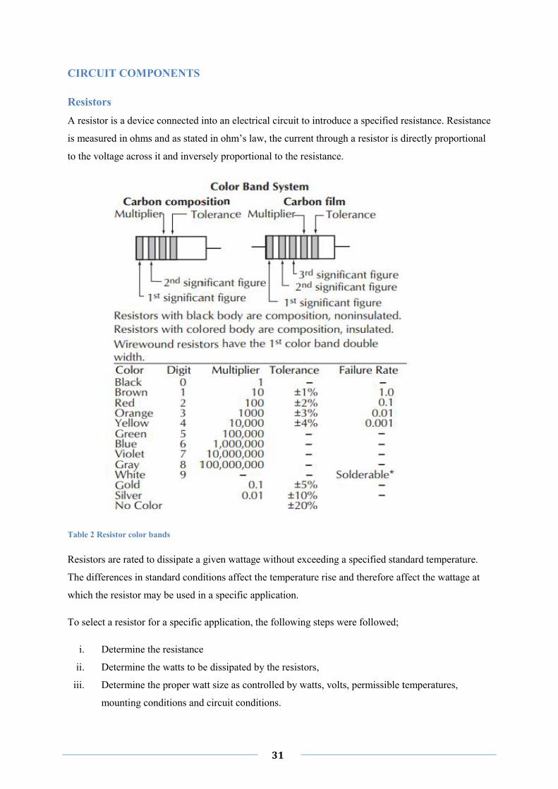
CIRCUIT COMPONENTS
Resistors
A resistor is a device connected into an electrical circuit to introduce a specified resistance. Resistan
is measured in ohms and as stated in ohm’s law, the current through a resistor is directly proportional
to the voltage across it and inversely proportional to the resistance.
Table 2 Resistor color bands
Resistors are rated to dissipate a given wattage without exceeding a specified standard temperature.
The differences in standard conditions affect
which the resistor may be used in a specific application.
To select a resistor for a specific application, the following steps were followed;
i. Determine the resistance
ii. Determine the watts to be dissipated by the resistors,
iii. Determine the proper watt size as controlled by watts, volts, permissible temperatures,
mounting conditions and circuit conditions.
31
A resistor is a device connected into an electrical circuit to introduce a specified resistance. Resistan
is measured in ohms and as stated in ohm’s law, the current through a resistor is directly proportional
to the voltage across it and inversely proportional to the resistance.
dissipate a given wattage without exceeding a specified standard temperature.
differences in standard conditions affect the temperature rise and therefore affect the wattage at
which the resistor may be used in a specific application.
tor for a specific application, the following steps were followed;
Determine the resistance
Determine the watts to be dissipated by the resistors,
Determine the proper watt size as controlled by watts, volts, permissible temperatures,
nd circuit conditions.
A resistor is a device connected into an electrical circuit to introduce a specified resistance. Resistance
is measured in ohms and as stated in ohm’s law, the current through a resistor is directly proportional
dissipate a given wattage without exceeding a specified standard temperature.
the temperature rise and therefore affect the wattage at
Determine the proper watt size as controlled by watts, volts, permissible temperatures,
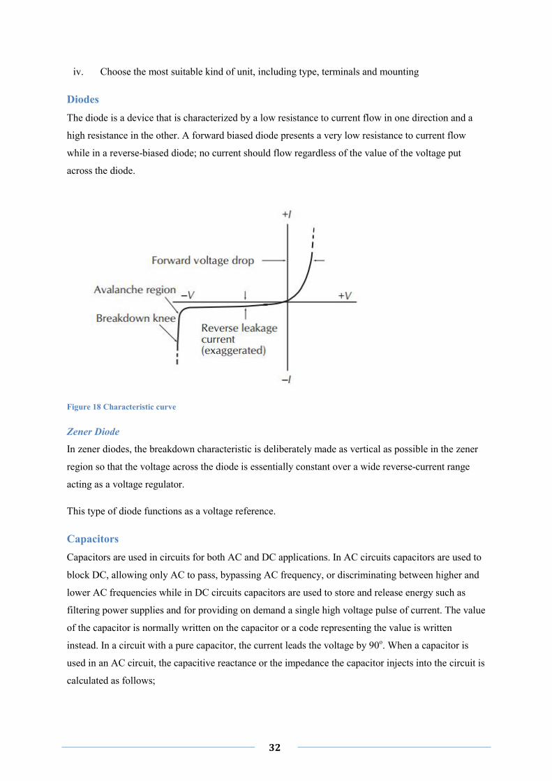
iv. Choose the most suitable kind of unit, including type, terminals and mounting
Diodes
The diode is a device that is characterized by a low resistance to current flow
high resistance in the other. A forward biase
while in a reverse-biased diode; no current should flow regardless of the value of the voltage put
across the diode.
Figure 18 Characteristic curve
Zener Diode
In zener diodes, the breakdown characteristic is deliberately made as vertical as possible in the zener
region so that the voltage across the diode is essentially constant over a wide reverse
acting as a voltage regulator.
This type of diode functions as a
Capacitors
Capacitors are used in circuits for both AC and DC applications. In AC circuits capacitors are used to
block DC, allowing only AC to pass, bypassing AC frequency, or discriminating between higher and
lower AC frequencies while in DC circuits capacitors are used to store and release energy such as
filtering power supplies and for providing on demand a single high voltage pulse of current. The value
of the capacitor is normally written on the capacitor or a code representing the
instead. In a circuit with a pure capacitor, the current leads the voltage by 90
used in an AC circuit, the capacitive reactance or the impedance the capacitor injects into the
calculated as follows;
32
Choose the most suitable kind of unit, including type, terminals and mounting
The diode is a device that is characterized by a low resistance to current flow in one direction and a
high resistance in the other. A forward biased diode presents a very low resistance to current flow
biased diode; no current should flow regardless of the value of the voltage put
s, the breakdown characteristic is deliberately made as vertical as possible in the zener
region so that the voltage across the diode is essentially constant over a wide reverse
This type of diode functions as a voltage reference.
Capacitors are used in circuits for both AC and DC applications. In AC circuits capacitors are used to
block DC, allowing only AC to pass, bypassing AC frequency, or discriminating between higher and
e in DC circuits capacitors are used to store and release energy such as
filtering power supplies and for providing on demand a single high voltage pulse of current. The value
of the capacitor is normally written on the capacitor or a code representing the value is written
instead. In a circuit with a pure capacitor, the current leads the voltage by 90o. When
AC circuit, the capacitive reactance or the impedance the capacitor injects into the
Choose the most suitable kind of unit, including type, terminals and mounting
in one direction and a
d diode presents a very low resistance to current flow
biased diode; no current should flow regardless of the value of the voltage put
s, the breakdown characteristic is deliberately made as vertical as possible in the zener
region so that the voltage across the diode is essentially constant over a wide reverse-current range
Capacitors are used in circuits for both AC and DC applications. In AC circuits capacitors are used to
block DC, allowing only AC to pass, bypassing AC frequency, or discriminating between higher and
e in DC circuits capacitors are used to store and release energy such as
filtering power supplies and for providing on demand a single high voltage pulse of current. The value
value is written
When a capacitor is
AC circuit, the capacitive reactance or the impedance the capacitor injects into the circuit is

Where Xc is the capacitive reactance, and
Uses of Capacitors
i. Filter
ii. Tune
iii. Couple
iv. Block DC
v. Shift phase
Transistors
A transistor is a semiconductor device used to amplify or switch electronic signals and electrical
power. Transistors are named by the way they are made. During the making
junction, the impurity content of the
are two types of transistors, a bipolar junction transistor (BJT) with terminals labeled base, collector
and emitter and field effect transistor (FET) with terminals labeled gate, source and dra
A bipolar junction transistor is the primary building block of most audio power amplifiers.
Heat sinks
Electrical systems are powered by smaller devices packaged in smaller systems that generate heat. To
manage the heat generated and dissipated, heat
conduct the heat and prevent the devices from damage. Heat sinks manage the heat generated through
heat transfer and there are three forms of heat transfer, namely;
i. Convection
33
=1
2
is the capacitive reactance, and F is the frequency in hertz and C is the capacitance in farads
vi. Start motors
vii. Feed through
viii. Compensate
ix. Isolate
x. Store energy
xi.
xii.
xiii.
A transistor is a semiconductor device used to amplify or switch electronic signals and electrical
power. Transistors are named by the way they are made. During the making of the material for a
content of the semiconductor is altered to provide NPN or PNP regions. There
are two types of transistors, a bipolar junction transistor (BJT) with terminals labeled base, collector
and emitter and field effect transistor (FET) with terminals labeled gate, source and dra
A bipolar junction transistor is the primary building block of most audio power amplifiers.
Electrical systems are powered by smaller devices packaged in smaller systems that generate heat. To
manage the heat generated and dissipated, heat sinks are attached to this devices or components to
conduct the heat and prevent the devices from damage. Heat sinks manage the heat generated through
heat transfer and there are three forms of heat transfer, namely;
C is the capacitance in farads
Suppress noise
Bypass
Pass AC
A transistor is a semiconductor device used to amplify or switch electronic signals and electrical
of the material for a
semiconductor is altered to provide NPN or PNP regions. There
are two types of transistors, a bipolar junction transistor (BJT) with terminals labeled base, collector
and emitter and field effect transistor (FET) with terminals labeled gate, source and drain.
A bipolar junction transistor is the primary building block of most audio power amplifiers.
Electrical systems are powered by smaller devices packaged in smaller systems that generate heat. To
sinks are attached to this devices or components to
conduct the heat and prevent the devices from damage. Heat sinks manage the heat generated through
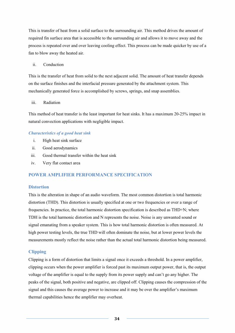
34
This is transfer of heat from a solid surface to the surrounding air. This method drives the amount of
required fin surface area that is accessible to the surrounding air and allows it to move away and the
process is repeated over and over leaving cooling effect. This process can be made quicker by use of a
fan to blow away the heated air.
ii. Conduction
This is the transfer of heat from solid to the next adjacent solid. The amount of heat transfer depends
on the surface finishes and the interfacial pressure generated by the attachment system. This
mechanically generated force is accomplished by screws, springs, and snap assemblies.
iii. Radiation
This method of heat transfer is the least important for heat sinks. It has a maximum 20-25% impact in
natural convection applications with negligible impact.
Characteristics of a good heat sink
i. High heat sink surface
ii. Good aerodynamics
iii. Good thermal transfer within the heat sink
iv. Very flat contact area
POWER AMPLIFIER PERFORMANCE SPECIFICATION
Distortion
This is the alteration in shape of an audio waveform. The most common distortion is total harmonic
distortion (THD). This distortion is usually specified at one or two frequencies or over a range of
frequencies. In practice, the total harmonic distortion specification is described as THD+N; where
TDH is the total harmonic distortion and N represents the noise. Noise is any unwanted sound or
signal emanating from a speaker system. This is how total harmonic distortion is often measured. At
high power testing levels, the true THD will often dominate the noise, but at lower power levels the
measurements mostly reflect the noise rather than the actual total harmonic distortion being measured.
Clipping
Clipping is a form of distortion that limits a signal once it exceeds a threshold. In a power amplifier,
clipping occurs when the power amplifier is forced past its maximum output power, that is, the output
voltage of the amplifier is equal to the supply from its power supply and can’t go any higher. The
peaks of the signal, both positive and negative, are clipped off. Clipping causes the compression of the
signal and this causes the average power to increase and it may be over the amplifier’s maximum
thermal capabilities hence the amplifier may overheat.
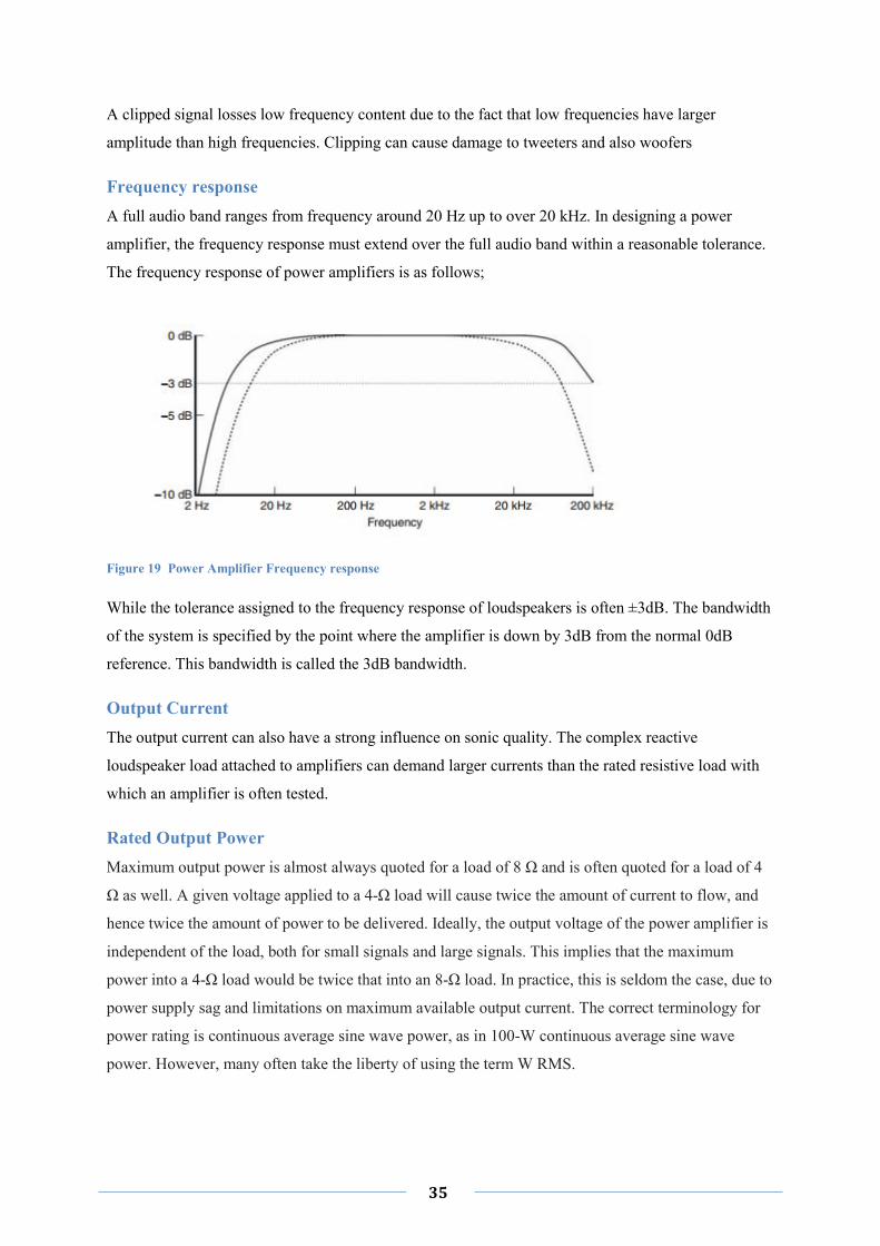
A clipped signal losses low frequency content due to the f
amplitude than high frequencies. Clipping can cause damage to tweeters and also woofers
Frequency response
A full audio band ranges from frequency around 20 Hz
amplifier, the frequency response must extend over the full audio band within a reasonable tolerance.
The frequency response of power amplifiers is as follows;
Figure 19 Power Amplifier Frequency response
While the tolerance assigned to the frequ
of the system is specified by the point where the amplifier is down by 3dB from the normal 0dB
reference. This bandwidth is called the 3dB bandwidth.
Output Current
The output current can also have
loudspeaker load attached to amplifiers can demand larger currents than the rated resistive load with
which an amplifier is often tested.
Rated Output Power
Maximum output power is almost always qu
Ω as well. A given voltage applied to a 4
hence twice the amount of power to be delivered. Ide
independent of the load, both for small
power into a 4-Ω load would be twice that into an 8
power supply sag and limitations on ma
power rating is continuous average
power. However, many often take the liberty of using
35
A clipped signal losses low frequency content due to the fact that low frequencies have larger
amplitude than high frequencies. Clipping can cause damage to tweeters and also woofers
A full audio band ranges from frequency around 20 Hz up to over 20 kHz. In designing a power
quency response must extend over the full audio band within a reasonable tolerance.
The frequency response of power amplifiers is as follows;
Power Amplifier Frequency response
While the tolerance assigned to the frequency response of loudspeakers is often ±3dB. The bandwidth
of the system is specified by the point where the amplifier is down by 3dB from the normal 0dB
reference. This bandwidth is called the 3dB bandwidth.
The output current can also have a strong influence on sonic quality. The complex reactive
loudspeaker load attached to amplifiers can demand larger currents than the rated resistive load with
which an amplifier is often tested.
Maximum output power is almost always quoted for a load of 8 Ω and is often quoted
Ω as well. A given voltage applied to a 4-Ω load will cause twice the amount of current to flow, and
hence twice the amount of power to be delivered. Ideally, the output voltage of the
ent of the load, both for small signals and large signals. This implies that the maximum
be twice that into an 8-Ω load. In practice, this is seldom the case, due to
sag and limitations on maximum available output current. The correct
average sine wave power, as in 100-W continuous average sine wave
often take the liberty of using the term W RMS.
act that low frequencies have larger
amplitude than high frequencies. Clipping can cause damage to tweeters and also woofers
up to over 20 kHz. In designing a power
quency response must extend over the full audio band within a reasonable tolerance.
ency response of loudspeakers is often ±3dB. The bandwidth
of the system is specified by the point where the amplifier is down by 3dB from the normal 0dB
a strong influence on sonic quality. The complex reactive
loudspeaker load attached to amplifiers can demand larger currents than the rated resistive load with
and is often quoted for a load of 4
amount of current to flow, and
ally, the output voltage of the power amplifier is
signals and large signals. This implies that the maximum
ad. In practice, this is seldom the case, due to
The correct terminology for
average sine wave
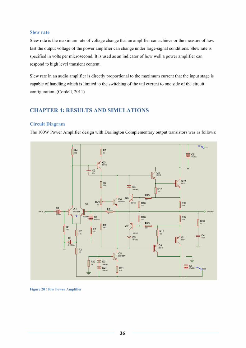
Slew rate
Slew rate is the maximum rate of voltage change that an amplifier can achieve
fast the output voltage of the power amplifier can change under large
specified in volts per microsecond. It is used
respond to high level transient content.
Slew rate in an audio amplifier is directly proportional to the maximum current that the input stage is
capable of handling which is limited to the switching of the tail current to one side of the circu
configuration. (Cordell, 2011)
CHAPTER 4: RESULTS AND SIMULATIONS
Circuit Diagram
The 100W Power Amplifier design with Darlington Complementary output transistors was as follows;
Figure 20 100w Power Amplifier
36
of voltage change that an amplifier can achieve or
fast the output voltage of the power amplifier can change under large-signal conditions. Slew rate is
specified in volts per microsecond. It is used as an indicator of how well a power a
respond to high level transient content.
Slew rate in an audio amplifier is directly proportional to the maximum current that the input stage is
capable of handling which is limited to the switching of the tail current to one side of the circu
CHAPTER 4: RESULTS AND SIMULATIONS
The 100W Power Amplifier design with Darlington Complementary output transistors was as follows;
the measure of how
signal conditions. Slew rate is
as an indicator of how well a power amplifier can
Slew rate in an audio amplifier is directly proportional to the maximum current that the input stage is
capable of handling which is limited to the switching of the tail current to one side of the circuit
The 100W Power Amplifier design with Darlington Complementary output transistors was as follows;
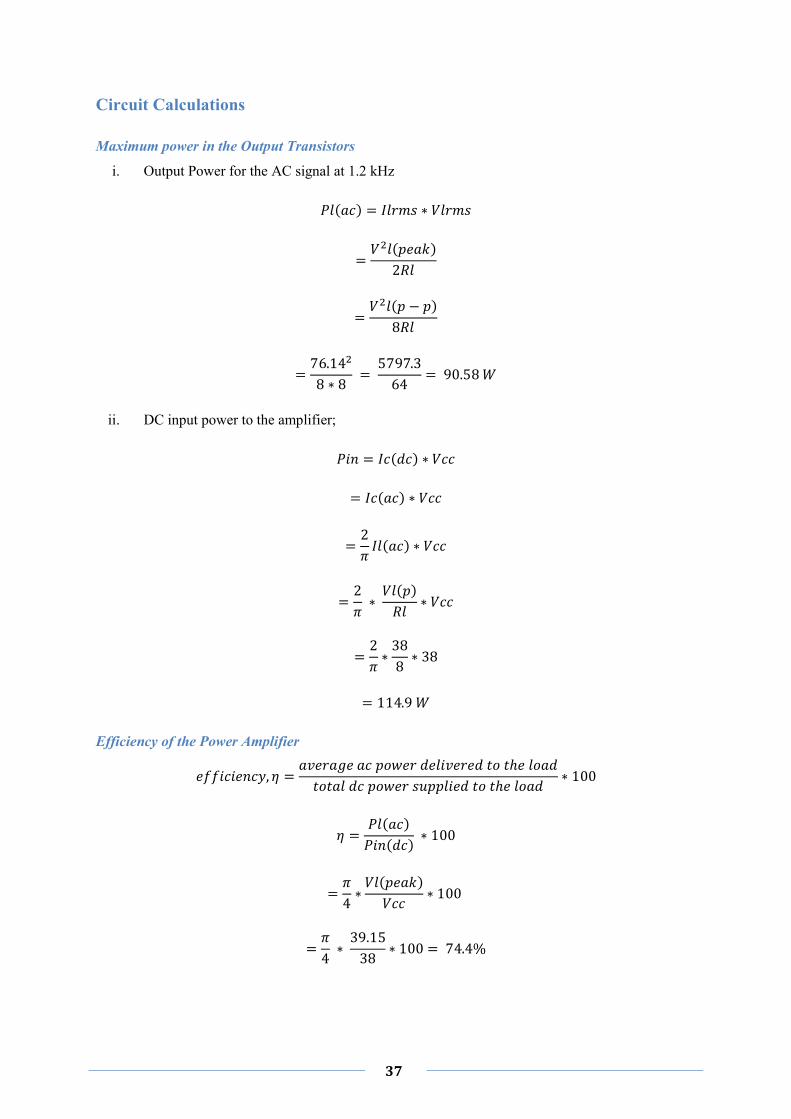
37
Circuit Calculations
Maximum power in the Output Transistors
i. Output Power for the AC signal at 1.2 kHz
() = ∗
=()
2
=( − )
8
=76.14
8 ∗ 8 =
5797.3
64= 90.58
ii. DC input power to the amplifier;
= () ∗
= () ∗
=2
() ∗
=2
∗
()
∗
=2
∗
38
8∗ 38
= 114.9
Efficiency of the Power Amplifier
, = ℎ
ℎ ∗ 100
=()
() ∗ 100
=
4∗
()
∗ 100
=
4 ∗
39.15
38∗ 100 = 74.4%
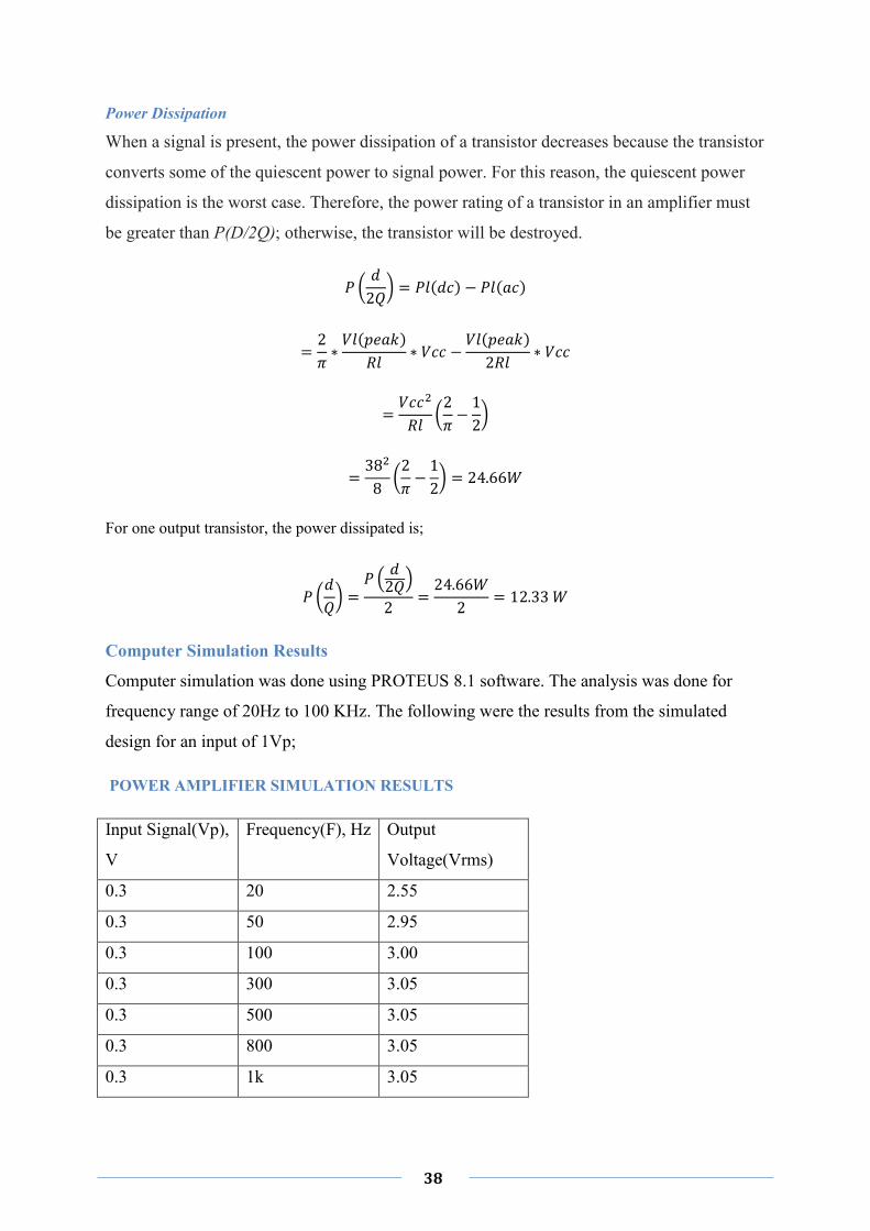
38
Power Dissipation
When a signal is present, the power dissipation of a transistor decreases because the transistor
converts some of the quiescent power to signal power. For this reason, the quiescent power
dissipation is the worst case. Therefore, the power rating of a transistor in an amplifier must
be greater than P(D/2Q); otherwise, the transistor will be destroyed.
2 = () − ()
=2
∗
()
∗ −
()
2∗
=
2
−
1
2
=38
8
2
−
1
2 = 24.66
For one output transistor, the power dissipated is;
=
2
2=
24.66
2= 12.33
Computer Simulation Results
Computer simulation was done using PROTEUS 8.1 software. The analysis was done for
frequency range of 20Hz to 100 KHz. The following were the results from the simulated
design for an input of 1Vp;
POWER AMPLIFIER SIMULATION RESULTS
Input Signal(Vp),
V
Frequency(F), Hz Output
Voltage(Vrms)
0.3 20 2.55
0.3 50 2.95
0.3 100 3.00
0.3 300 3.05
0.3 500 3.05
0.3 800 3.05
0.3 1k 3.05
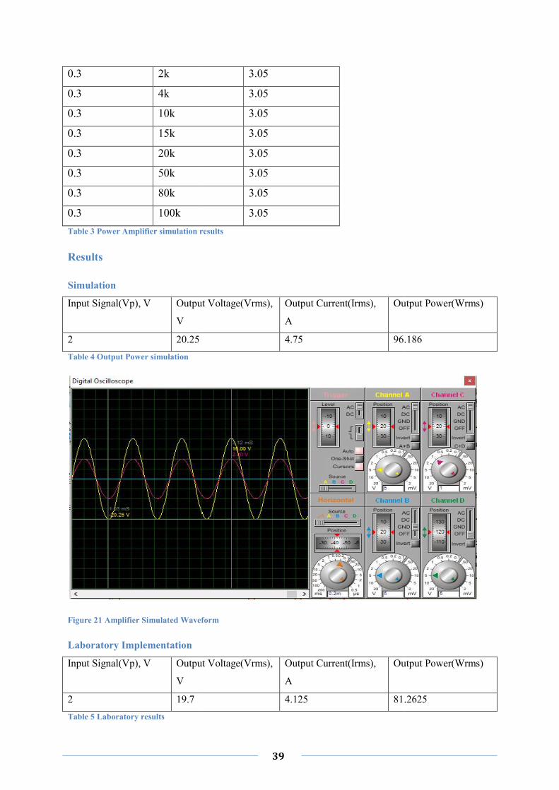
0.3 2k
0.3 4k
0.3 10k
0.3 15k
0.3 20k
0.3 50k
0.3 80k
0.3 100k
Table 3 Power Amplifier simulation results
Results
Simulation
Input Signal(Vp), V Output Voltage(Vrms),
V
2 20.25
Table 4 Output Power simulation
Figure 21 Amplifier Simulated Waveform
Laboratory Implementation
Input Signal(Vp), V Output Voltage(Vrms),
V
2 19.7
Table 5 Laboratory results
39
3.05
3.05
3.05
3.05
3.05
3.05
3.05
3.05
Power Amplifier simulation results
Output Voltage(Vrms), Output Current(Irms),
A
Output Power(Wrms)
4.75 96.186
Amplifier Simulated Waveform
Output Voltage(Vrms), Output Current(Irms),
A
Output Power(Wrms)
4.125 81.2625
Output Power(Wrms)
96.186
Output Power(Wrms)
81.2625

40
Figure 22 Laboratory Waveform
POWER AMPLIFIER FREQUENCY RESPONSE
FREQUENCY (KHz) VIN(V) VOUT(V) GAIN
1 1 18.3 18.3
10 1 18.4 18.4
20 1 18.4 18.4
30 1 18.5 18.5
40 1 18.5 18.5
50 1 18.5 18.5
60 1 18.7 18.7
70 1 18.7 18.7
80 1 18.7 18.7
90 1 18.8 18.8
100 1 18.8 18.8
Table 6POWER AMPLIFIER FREQUENCY RESPONSE
FILTER DESIGN SIMULATION RESULTS
A signal generator was connected to the input of the circuit and a CRO at the output as shown below.
The signal generator was adjusted such that it gave out a voltage of 5 divisions peak at 0.2v/div. This
translated to an input voltage of 1Volt peak.
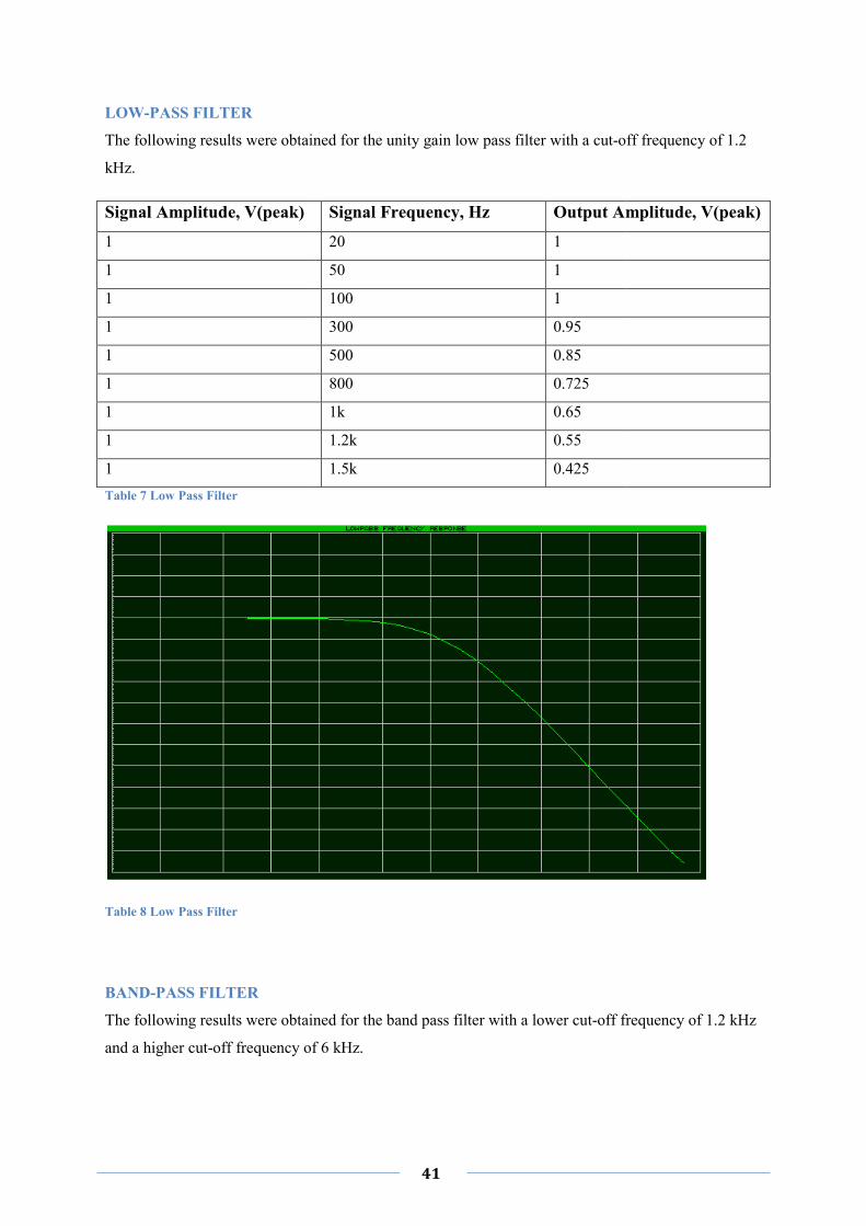
LOW-PASS FILTER
The following results were obtained for the unity gain low pass filter wit
kHz.
Signal Amplitude, V(peak)
1
1
1
1
1
1
1
1
1
Table 7 Low Pass Filter
Table 8 Low Pass Filter
BAND-PASS FILTER
The following results were obtained for the band pass filter with a lower cut
and a higher cut-off frequency of 6
41
The following results were obtained for the unity gain low pass filter with a cut-off frequency of 1.2
Signal Frequency, Hz Output Amplitude, V(peak)
20 1
50 1
100 1
300 0.95
500 0.85
800 0.725
1k 0.65
1.2k 0.55
1.5k 0.425
The following results were obtained for the band pass filter with a lower cut-off frequency of 1.2 kHz
off frequency of 6 kHz.
off frequency of 1.2
Output Amplitude, V(peak)
off frequency of 1.2 kHz
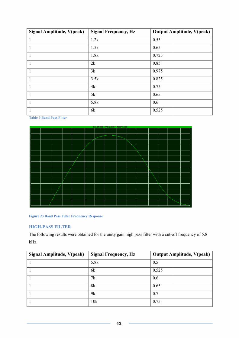
Signal Amplitude, V(peak)
1
1
1
1
1
1
1
1
1
1
Table 9 Band Pass Filter
Figure 23 Band Pass Filter Frequency Response
HIGH-PASS FILTER
The following results were obtained for the unity gain high pass filter with a cut
kHz.
Signal Amplitude, V(peak)
1
1
1
1
1
1
42
Signal Frequency, Hz Output Amplitude, V(peak)
1.2k 0.55
1.5k 0.65
1.8k 0.725
2k 0.85
3k 0.975
3.5k 0.825
4k 0.75
5k 0.65
5.8k 0.6
6k 0.525
r Frequency Response
The following results were obtained for the unity gain high pass filter with a cut-off frequency of 5.8
Signal Frequency, Hz Output Amplitude, V(peak)
5.8k 0.5
6k 0.525
7k 0.6
8k 0.65
9k 0.7
10k 0.75
Output Amplitude, V(peak)
off frequency of 5.8
Output Amplitude, V(peak)
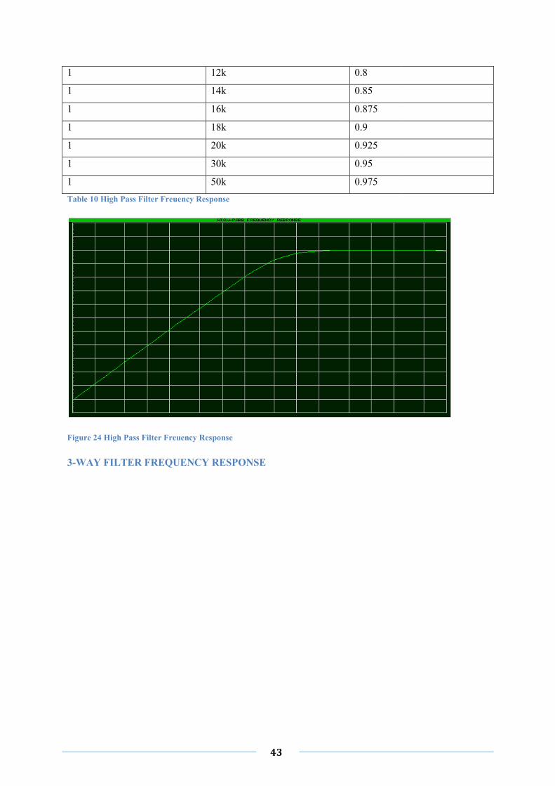
1
1
1
1
1
1
1
Table 10 High Pass Filter Freuency Response
Figure 24 High Pass Filter Freuency Response
3-WAY FILTER FREQUENCY RESPONSE
43
12k 0.8
14k 0.85
16k 0.875
18k 0.9
20k 0.925
30k 0.95
50k 0.975
High Pass Filter Freuency Response
High Pass Filter Freuency Response
WAY FILTER FREQUENCY RESPONSE
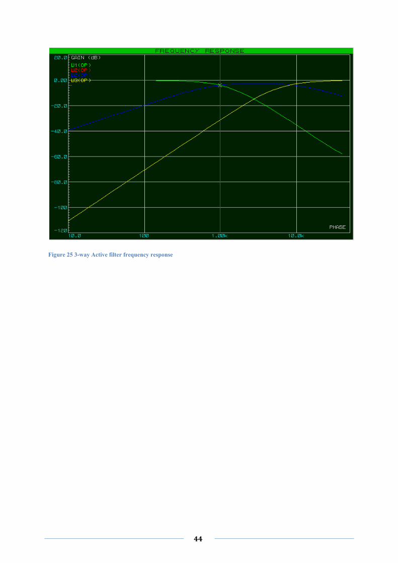
Figure 25 3-way Active filter frequency response
44
way Active filter frequency response

45
CHAPTER 5
5.1 DISCUSSION
The 100 watt power amplifier with a Darlington complementary output transistor was simulated and
eventually fabricated on a Printed Circuit Board. As explained in the project, a 3-way active filter was
designed to produce output at different frequencies.
The measured power 96.18 Watts was close to our expected value. For the active filters, the
experimental results differ a bit from the simulated results when the two gain responses of each
network are compared. This is because some of the components used in the circuit are not the exact
values of the simulation components and moreover, some of them were rounded off to the nearest
standard value. Component tolerance could also be a cause of the difference as they are about 5% and
above.
The graphical results above show fairly similar performances of each of the crossover networks. The
low pass and high pass filters show a unity gain over the pass-band up until the cutoff frequency.
5.2 CONCLUSION
The main objectives of this project were to come up with a 100watts power amplifier with a
Darlington complementary symmetry output power transistors for use in a 3-way active
crossover network. That is:-
A 100W power amplifier with Darlington complementary symmetry output transistor
Design a 3-way active crossover network consisting of a high-pass, band-pass, and a
low-pass filter
Test the complete power amplifier built and verify it works.
These objectives were met and the designs were implemented through simulation and
breadboard testing before final fabrication of components on the printed circuit board (PCB).
The audio output of the power amplifier was of high quality with minimal distortion since
each filter drove its own specified frequency band hence producing the best sound quality
on the basis of their capability.
The experimental errors of the project were at a minimal since before soldering components
on the PCB, test was done through simulation using the Proteus 8.1 software. After the
simulation, to further reduce any remaining errors, the components were placed on a
breadboard and tested in the laboratory and the results obtained for both simulation and
testing were tabulated in the results section of chapter four.

46
47
5.3 RECOMMENDATION
The Darlington complementary transistors, TIP33C and TIP34C used in the output of the
amplifier produced high current which caused high power dissipation that damaged the
transistors hence I would recommend use of a large heat sink to conduct the heat.
The use of other power transistors with less power could also solve the overheating while
also paralleling of the Darlington power transistors to share the high current could also solve
the high current problem.
Further improvement is required to achieve the objective of this project. The design should be
modified to reduce the size of the circuitry through the use of integrated circuits (IC) on the
input and voltage amplification stage.
48
REFERENCES
1. Handbook for Sound Engineers, Edited by Glen Ballou
2. Basic Electricity and Electronics, 4th Edition
3. Designing of Audio Power Amplifiers by Bob Cordell
4. www.futureelectronics.com/en/transistors/darlington-transistors.aspx
5. www.learnabout-electronics.org
6. FEE 302 Analog Electronics Class notes by Dr. Kamucha
7. Power Electronics Handbook – Rashid
8. M. E. Meserve, "Band-Pass Active Filter Designer," Band-Pass Active Filter
Designer, p. 5.
9. JJC, "Active Filter Design (Sallen-Key Filter)," Electrical Engineering Junior Lab, p.
8, 9/7/02.
10. A.B. Williams, Electronic Filter Design Handbook, McGraw-Hill, 1981.
11. H. Zumbahlen, Passive and Active Filtering, Analog Devices.
12. S. P. Laboratory, Analog Electronics, Active Filters, CALIFORNIA: CALIFORNIA
INSTITUTE OF TECHNOLOGY, Revision December 2012.
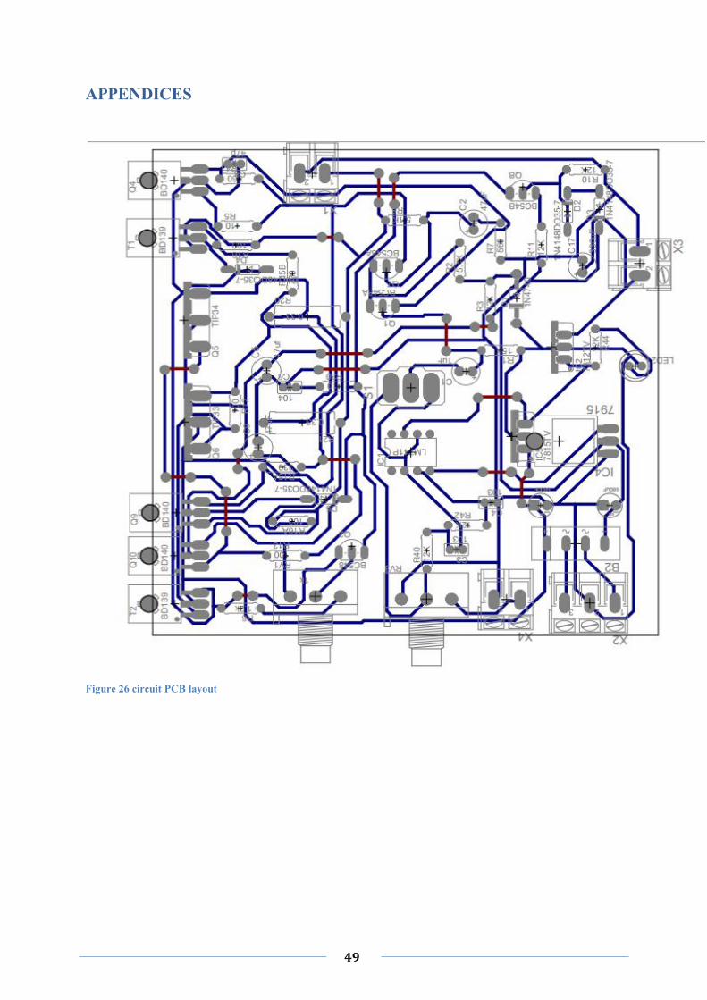
APPENDICES
Figure 26 circuit PCB layout
49
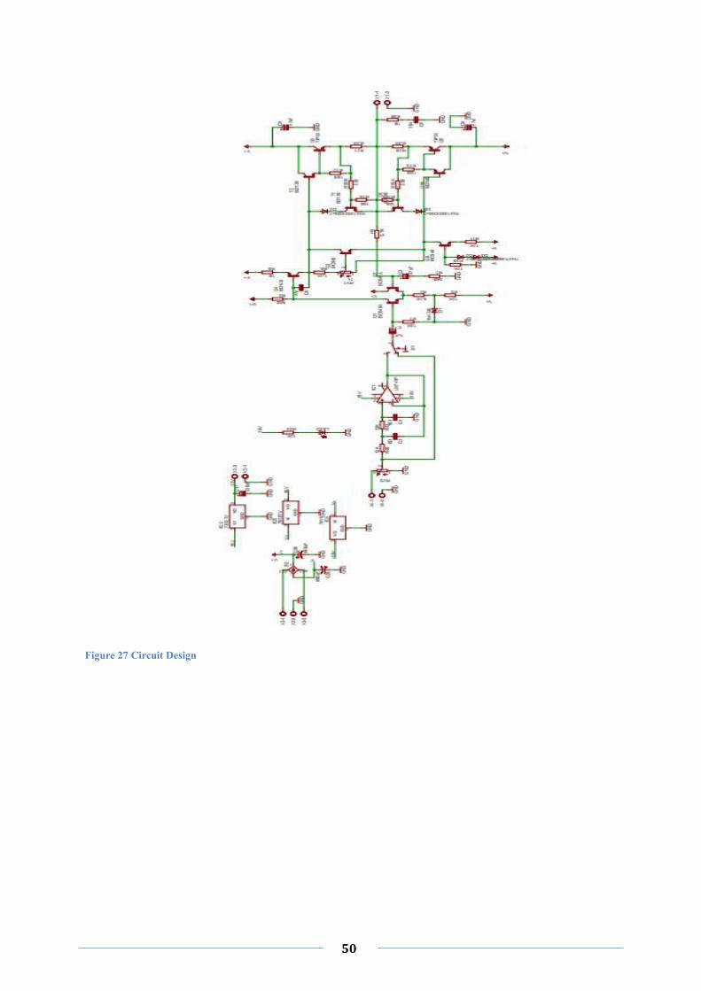
Figure 27 Circuit Design
50