Design and Optimization of An All Optically Driven MEMS ......Design and Optimization of An All...
27
Design and Optimization of An All Optically Driven Phase Correction MEMS Device using FEA V. Mathur , K.Anglin, V.S. Prasher, K.Tremkoa, S.R. Vangala, X. Qian, W.D. Goodhue Department of Physics and Applied Physics,University of Massachusetts,Lowell B Haji-Saeed, Jed Khoury Air Force Research Laboratory/SNHC,Hanscom Air Force Base,MA-01731 Presented at the COMSOL Conference 2009 Boston
Transcript of Design and Optimization of An All Optically Driven MEMS ......Design and Optimization of An All...
Design and Optimization of An All Optically Driven Phase
Correction MEMS Device using FEA
V. Mathur, K.Anglin, V.S. Prasher, K.Tremkoa, S.R. Vangala, X. Qian, W.D. Goodhue
Department of Physics and Applied Physics,University of Massachusetts,Lowell
B Haji-Saeed, Jed KhouryAir Force Research Laboratory/SNHC,Hanscom Air Force Base,MA-01731
Presented at the COMSOL Conference 2009 Boston
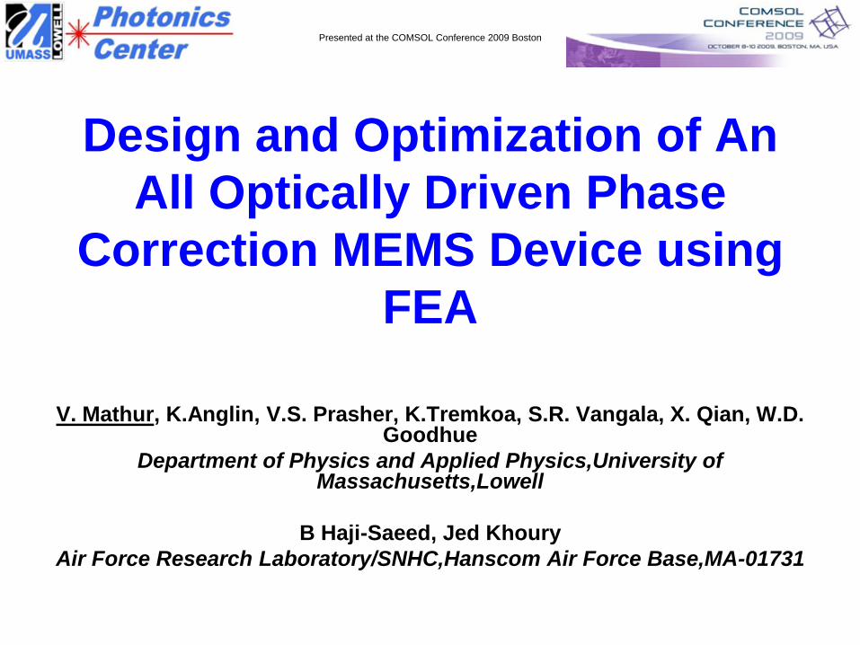
Outline• Introduction and working principle
• Micro mirror (Structural Mechanics, Electrostatics module)
• Photodiode (Electrostatics, Conduction-Convection module)
• Wafer fusion (Thermal-structural module)
• Conclusion and future work
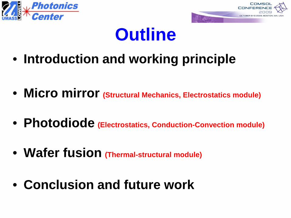
Introduction
• Wavefront aberrationcorrection
• Spatial light modulators• Moving MEMS mirrors for
dynamic correction
Image Credit: Canada-France-Hawaii Telescope. Starburst galaxy NGC7469
With AO Without AO
Medical Imaging (Human Retina)
Image courtesy Center for Adaptive Optics.
With AO Without AO
image credit: Center for Adaptive Optics
Astronomy
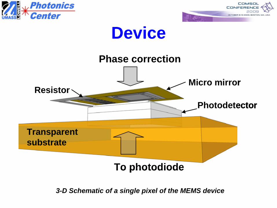
Device
To photodiode
Phase correction
Photodetector
Micro mirrorResistor
Transparent substrate
To photodiode
Phase correction
Photodetector
Micro mirrorResistor
To photodiode
Phase correction
Photodetector
Micro mirrorResistor
Transparent substrate
3-D Schematic of a single pixel of the MEMS device
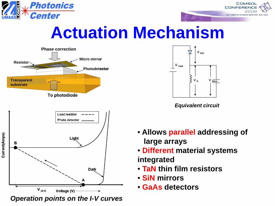
Actuation Mechanism
To photodiode
Phase correction
Photodetector
Micro mirrorResistor
Transparent substrate
To photodiode
Phase correction
Photodetector
Micro mirrorResistor
To photodiode
Phase correction
Photodetector
Micro mirrorResistor
Transparent substrate
V Mirror
V Total
V PIN
V R V Mirror
V Total
V PIN
V R
Equivalent circuit
Operation points on the I-V curves
• Allows parallel addressing of large arrays
• Different material systems integrated• TaN thin film resistors• SiN mirrors• GaAs detectors
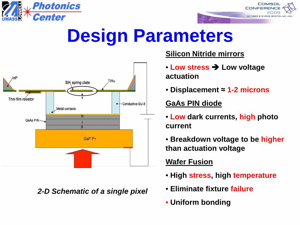
Design ParametersSilicon Nitride mirrors
• Low stress Low voltage actuation
• Displacement ≈ 1-2 microns
GaAs PIN diode
• Low dark currents, high photo current
• Breakdown voltage to be higherthan actuation voltage
Wafer Fusion
• High stress, high temperature
• Eliminate fixture failure
• Uniform bonding2-D Schematic of a single pixel
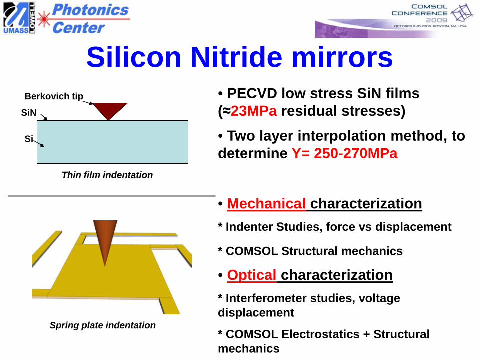
Silicon Nitride mirrors• PECVD low stress SiN films (≈23MPa residual stresses)• Two layer interpolation method, to determine Y= 250-270MPa
• Mechanical characterization* Indenter Studies, force vs displacement
* COMSOL Structural mechanics
• Optical characterization* Interferometer studies, voltage displacement
* COMSOL Electrostatics + Structural mechanics
Spring plate indentation
SiN
Si
Berkovich tip
Thin film indentation
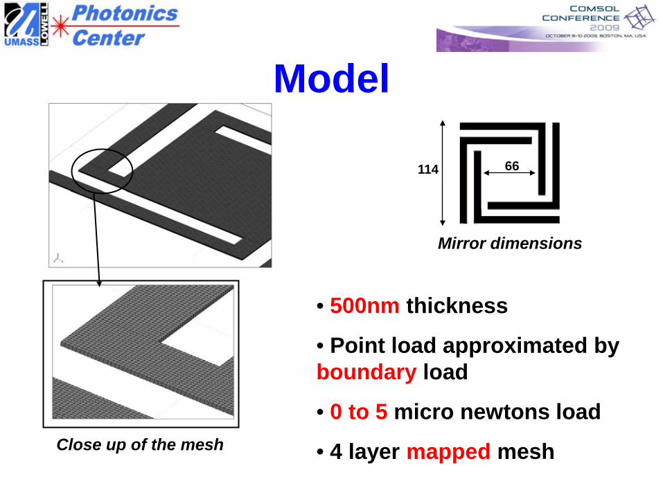
Model
66114
• 500nm thickness
• Point load approximated by boundary load
• 0 to 5 micro newtons load
• 4 layer mapped meshClose up of the mesh
Mirror dimensions
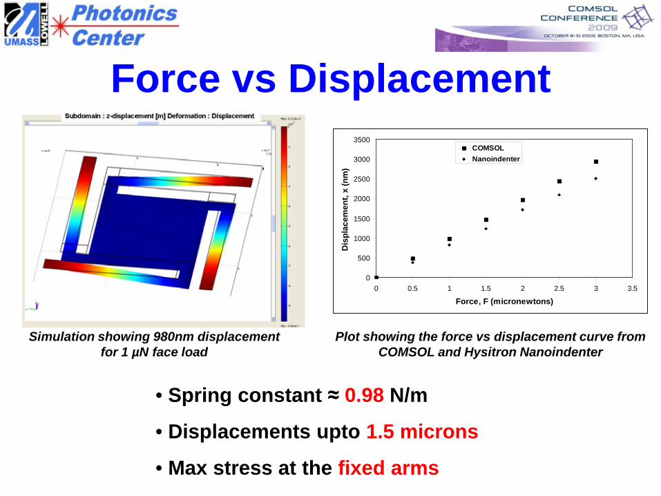
Force vs Displacement
0
500
1000
1500
2000
2500
3000
3500
0 0.5 1 1.5 2 2.5 3 3.5
Force, F (micronewtons)
Dis
plac
emen
t, x
(nm
)
COMSOLNanoindenter
• Spring constant ≈ 0.98 N/m
• Displacements upto 1.5 microns
• Max stress at the fixed arms
Simulation showing 980nm displacement for 1 µN face load
Plot showing the force vs displacement curve from COMSOL and Hysitron Nanoindenter
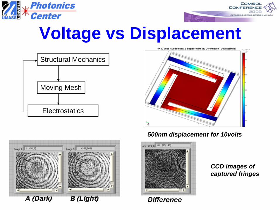
Voltage vs Displacement
500nm displacement for 10volts
Structural Mechanics
Moving Mesh
Electrostatics
CCD images of captured fringes
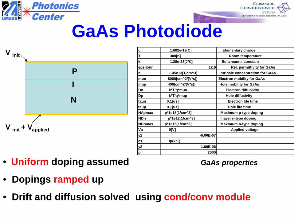
GaAs Photodiodeq 1.602e-19[C] Elementary charge T 300[K] Room temperature k 1.38e-23[J/K] Boltzmanns constant epsilonr 12.9 Rel. permittivity for GaAs ni 1.45e13[1/cm^3] Intrinsic concentration for GaAs mun 8000[cm^2/(V*s)] Electron mobility for GaAs mup 400[cm^2/(V*s)] Hole mobility for GaAs Dn k*T/q*mun Electron diffusivity Dp k*T/q*mup Hole diffusivity taun 0.1[us] Electron life time taup 0.1[us] Hole life time NApmax p*1e15[1/cm^3] Maximum p-type doping NDn p*1e12[1/cm^3] I layer n-type doping NDnmax p*1e15[1/cm^3] Maximum n-type doping Va 0[V] Applied voltage y1 -6.00E-07 c1 q/(k*T) y2 -1.60E-06 p 2000
PI
N
V init
V init + Vapplied
GaAs properties• Uniform doping assumed
• Dopings ramped up
• Drift and diffusion solved using cond/conv module
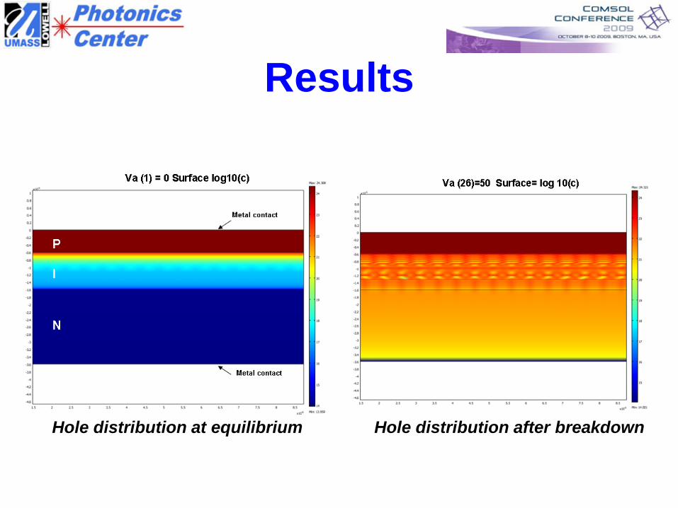
Results
Hole distribution at equilibrium Hole distribution after breakdown
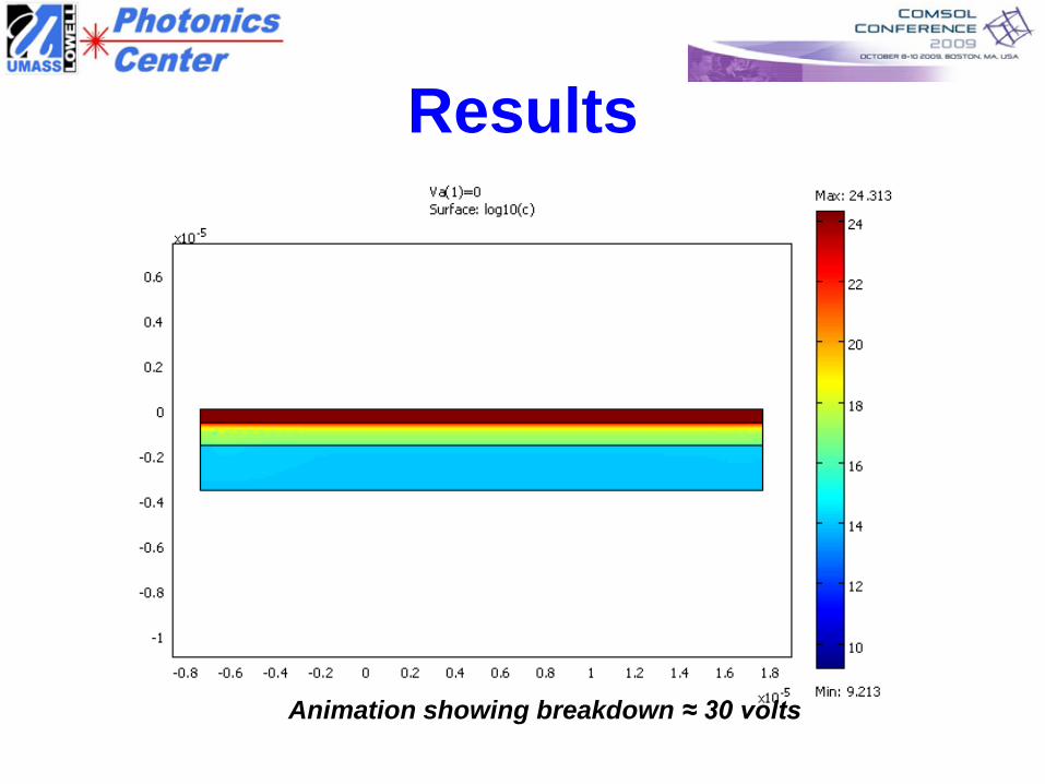
Results
Animation showing breakdown ≈ 30 volts
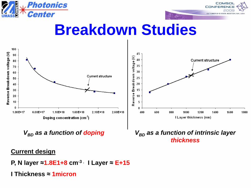
Breakdown Studies
VBD as a function of doping VBD as a function of intrinsic layer thickness
Current design
P, N layer ≈1.8E1+8 cm-3 , I Layer ≈ E+15
I Thickness ≈ 1micron
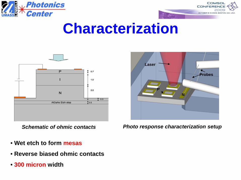
Characterization
Schematic of ohmic contacts
Laser
NP
Probes
Photo response characterization setup
• Wet etch to form mesas
• Reverse biased ohmic contacts
• 300 micron width
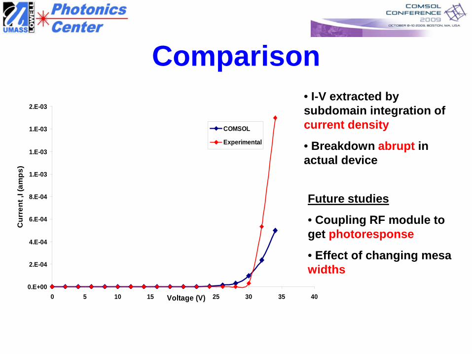
Comparison
0.E+00
2.E-04
4.E-04
6.E-04
8.E-04
1.E-03
1.E-03
1.E-03
2.E-03
0 5 10 15 20 25 30 35 40Voltage (V)
Cur
rent
,I (a
mps
)
COMSOL
Experimental
• I-V extracted by subdomain integration of current density
• Breakdown abrupt in actual device
Future studies
• Coupling RF module to get photoresponse
• Effect of changing mesa widths
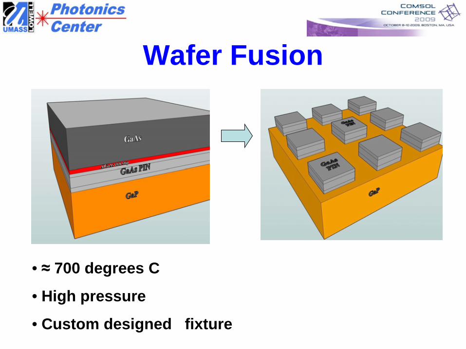
Wafer Fusion
• ≈ 700 degrees C
• High pressure
• Custom designed fixture
Wafer Fusion
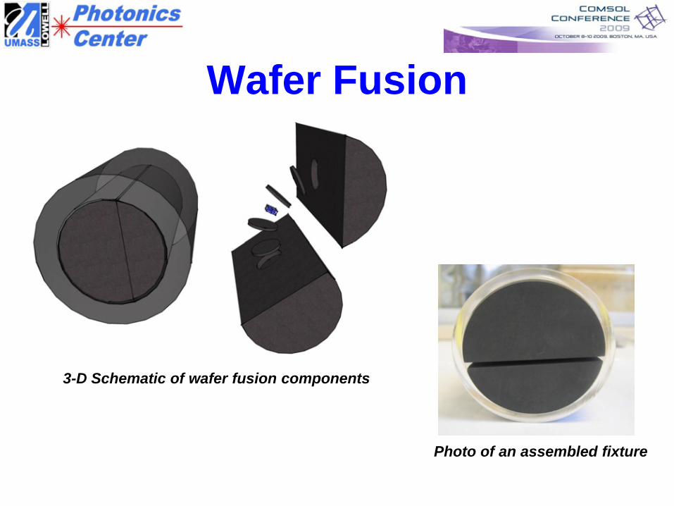
3-D Schematic of wafer fusion components
Photo of an assembled fixture
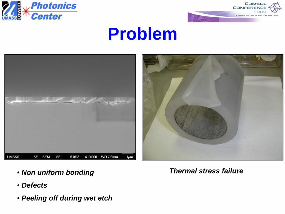
Problem
Thermal stress failure• Non uniform bonding
• Defects
• Peeling off during wet etch
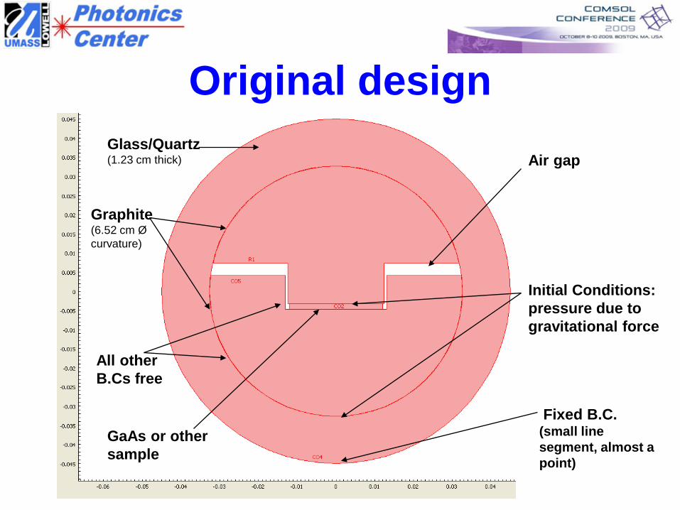
Original designGlass/Quartz (1.23 cm thick)
Graphite(6.52 cm Ø curvature)
Air gap
Fixed B.C. (small line segment, almost a point)
All other B.Cs free
Initial Conditions: pressure due to gravitational force
GaAs or other sample
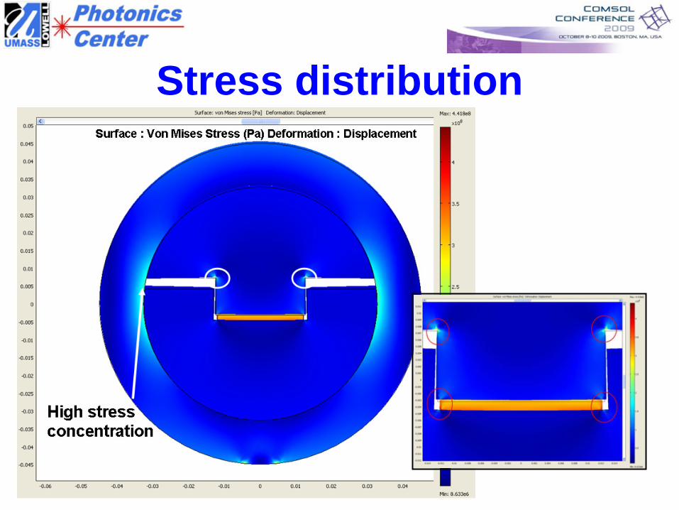
Stress distribution
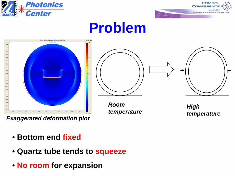
Problem
Room temperature
High temperature
Exaggerated deformation plot
• Bottom end fixed
• Quartz tube tends to squeeze
• No room for expansion
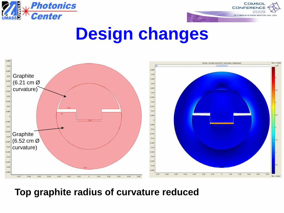
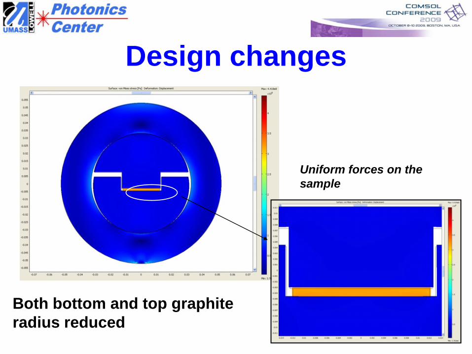
Design changes
Graphite(6.21 cm Ø curvature)
Graphite(6.52 cm Ø curvature)
Top graphite radius of curvature reduced
Design changes
Both bottom and top graphite radius reduced
Uniform forces on the sample
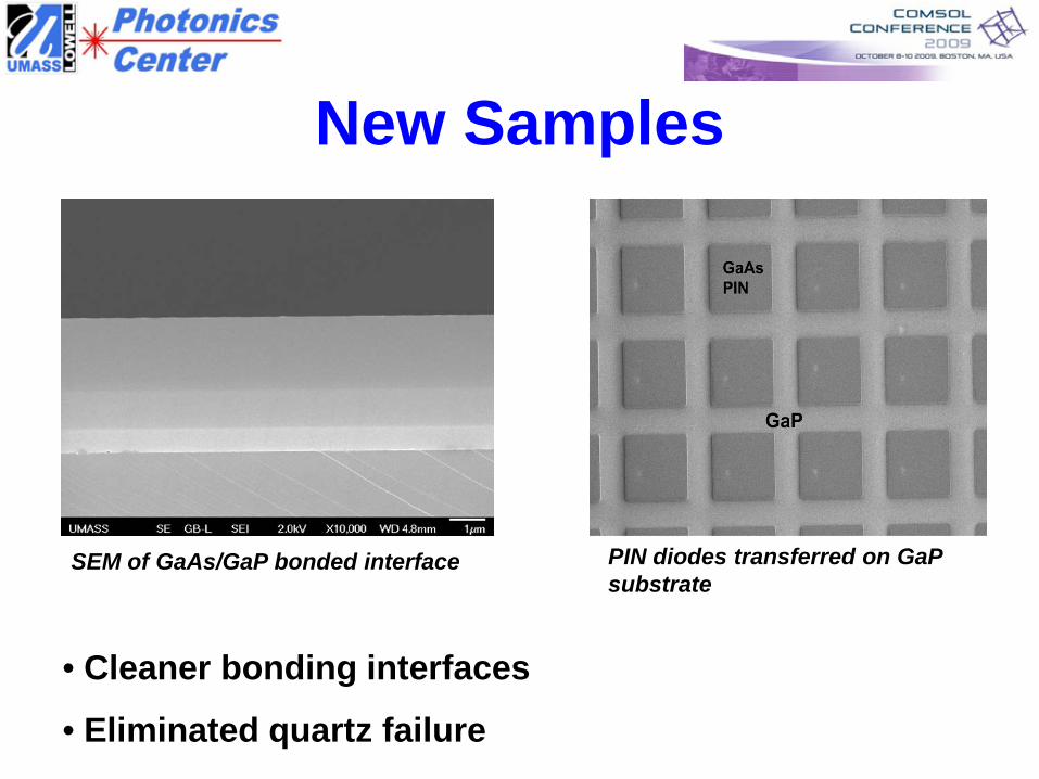
New Samples
• Cleaner bonding interfaces
• Eliminated quartz failure
PIN diodes transferred on GaP substrate
SEM of GaAs/GaP bonded interface
Conclusion & Future WorkBasic models developed :
to study the electrostatic actuation of spring plates
to study behaviour of our PIN diode structure
wafer fusion fixture
64 Bit workstation with 28Gb RAM
Future work :
• Study effect of changing spring plate thickness
• Varying PIN diode dimensions, and photo response

Acknowledgement•Work partially funded by United States Air Force
www. uml.edu/photonics