GAO Report - Preliminary Observations on the Implementation of Broadband Programs 10-27-2009
Upload
duongquynhCategory
view
213download
0
DESIGN AND IMPLEMENTATION OF A BROADBAND I-Q VECTOR MODULATOR AND A FEEDFORWARD LINEARIZER
FOR V/UHF BAND
A THESIS SUBMITTED TO THE GRADUATE SCHOOL OF NATURAL AND APPLIED SCIENCES
OF MIDDLE EAST TECHNICAL UNIVERSITY
BY
AYŞE ÜNLÜ ÖZKAYA
IN PARTIAL FULFILLMENT OF THE REQUIREMENTS FOR
THE DEGREE OF MASTER OF SCIENCE IN
ELECTRICAL AND ELECTRONICS ENGINEERING
FEBRUARY 2010

Approval of the thesis:
DESIGN AND IMPLEMENTATION OF A BROADBAND I-Q VECTOR MODULATOR AND A FEEDFORWARD LINEARIZER
FOR V/UHF BAND
submitted by AYŞE ÜNLÜ ÖZKAYA in partial fulfillment of the requirements for the degree of Master of Science in Electrical and Electronics Engineering Department, Middle East Technical University by, Prof. Dr. Canan Özgen _________ Dean, Graduate School of Natural and Applied Sciences Prof. Dr. Đsmet Erkmen _________ Head of Department, Electrical and Electronics Engineering Assoc. Prof. Dr. Şimşek Demir Supervisor, Electrical and Electronics Engineering Dept., METU _________ Examining Committee Members: Prof. Dr. Canan Toker ______________ Electrical and Electronics Engineering Dept., METU Assoc. Prof. Dr. Şimşek Demir ______________ Electrical and Electronics Engineering Dept., METU Prof. Dr. Nevzat Yıldırım ______________ Electrical and Electronics Engineering Dept., METU Assoc. Prof. Dr. Sencer Koç ______________ Electrical and Electronics Engineering Dept., METU Dr. A. Hakan Coşkun ______________ HC AEDTM, ASELSAN A.Ş. Date: 05.02.2010

iii
I hereby declare that all information in this document has been obtained and presented in accordance with academic rules and ethical conduct. I also declare that, as required by these rules and conduct, I have fully cited and referenced all material and results that are not original to this work.
Name, Last Name: Ayşe Ünlü Özkaya
Signature :

iv
ABSTRACT
DESIGN AND IMPLEMENTATION OF A BROADBAND I-Q VECTOR MODULATOR AND A FEEDFORWARD LINEARIZER
FOR V/UHF BAND
Özkaya Ünlü, Ayşe
M.Sc., Department of Electrical and Electronics Engineering
Supervisor: Assoc. Prof. Dr. Şimşek Demir
February 2010, 77 pages
Considering the requirements of the commercial and military applications on
amplitude and phase linearity, it is necessary to reduce nonlinearity of the
amplifiers. There are several linearization techniques that are used to reduce
nonlinearity effects. Feedforward linearization technique is known as one of the
best linearization methods due to its superior linearization performance and
broadband operation. Vector modulators which allows amplitude and phase
modulation simultaneously, is the most important component of a feedforward
system.
In this thesis, first of all a broadband V/UHF vector modulator designed and
implemented. Then a feedforward system is investigated and implemented using
the designed vector modulator for V/UHF band.
Key words: Vector Modulator, Feedforward, Linearization

v
ÖZ
V/UHF BANDI ĐÇĐN GENĐŞ BANTLI I-Q VEKTÖR MODÜLATÖR VE ĐLERĐBESLEME DOĞRUSALLAŞTIRMA YÖNTEMĐ TASARIMI VE
GERÇEKLENMESĐ
Özkaya Ünlü, Ayşe
Yüksek Lisans, Elektrik-Elektronik Mühendisliği Bölümü
Tez Yöneticisi: Doç. Dr. Şimşek Demir
Şubat 2010, 77 sayfa
Ticari ve askeri uygulamalardaki doğrusal genlik ve faz gereksinimleri göz önüne
alındığında, yükselteçlerin daha doğrusal çalışması ihtiyacı doğmaktadır.
Yükselteçlerin daha doğrusal çalışmasını sağlayacak birçok doğrusallaştırma
yöntemi bulunmaktadır. Đleribesleme yöntemi doğrusallaştırma performansı ve
geniş bantlı çalışabilme özelliği ile en iyi doğrusallaştırma yöntemlerinden
birisidir. Eş zamanlı genlik ve faz modülasyonuna izin veren vektör modülator ise
ileribesleme yönteminin en önemli elemanıdır.
Bu tezde öncelikle VHF bandında geniş bantlı çalışacak çalışacak bir vector
modülatör tasarlanmış ve gerçeklenmiştir. Daha sonraki aşamada yine VHF
bandında çalışacak bir ileribesleme sistemi, tasarlanmış olan vektör modülatör
kullanılarak gerçeklenmiştir.
Anahtar Kelimeler: Vektör Modülatör, Đleribesleme, Doğrusallaştırma

vi
To My Beloved Husband

vii
ACKNOWLEDGEMENTS
I would like to express my gratitude and deep appreciation to my supervisor
Assoc. Prof. Dr. Şimşek Demir for his guidance and positive suggestions.
I would like to thank Dr. A. Hakan Coşkun from Aselsan A.Ş. for contributions
to this work and sharing his technical facilities with me. I have learned much
from his suggestions and experiences. It is also my pleasure to thank my
colleague who provided me such a friendly work environment they provided.
I am also grateful to Aselsan Electronics Industries Inc. for not only giving me
the opportunity to improve my engineering capabilities but also providing me
every kind of software, hardware and financial support throughout the progress of
this work. I also would like to thank TÜBĐTAK for financial support offered
throughout the thesis.
Finally, I would like to deeply appreciate my beloved husband for his confidence
and endless support during this work. Also lots of thanks to my Mom, Dad, Sister
and Brother for their love, confidence and patience over the years. This thesis is
dedicated to them.

viii
TABLE OF CONTENTS
ABSTRACT ........................................................................................................... iv
ÖZ............................................................................................................................ v
ACKNOWLEDGEMENTS .................................................................................. vii
TABLE OF CONTENTS ..................................................................................... viii
LIST OF TABLES .................................................................................................. x
LIST OF FIGURES ................................................................................................ xi
LIST OF ABBREVIATIONS .............................................................................. xiii
1 INTRODUCTION ............................................................................................... 1
2 LINEARITY AND LINEARIZATION .............................................................. 5
2.1 Linearity Concept .................................................................................. 5
2.2 Linearization and linearization techniques ............................................ 8
2.2.1 Feedforward linearization ............................................................ 9
2.2.2 Predistortion ............................................................................... 12
2.2.3 LINC technique .......................................................................... 13
2.2.4 Envelope elimination and restoration (EER) technique ............. 14
3 I-Q VECTOR MODULATOR .......................................................................... 16
3.1 Vector modulator................................................................................. 16
3.2 I-Q Vector modulator .......................................................................... 17
3.2.1 PIN diodes .................................................................................. 20
3.3 Working principle of I-Q vector modulator ........................................ 22
3.4 Simulations of I-Q vector modulator circuit ....................................... 28
3.5 Determination of bias currents of PIN diodes ..................................... 32
3.6 Implementation of I-Q vector modulator ............................................ 32
4 IMPLEMENTATION OF FEEDFORWARD LINEARIZATION SYSTEM . 40
4.1 Carrier cancellation loop (CCL) .......................................................... 40
4.1.1 Directional couplers ................................................................... 41
4.1.2 Main amplifier ............................................................................ 46

ix
4.1.3 Delay lines and attenuators ........................................................ 51
4.1.4 Implementation of carrier cancellation loop .............................. 51
4.2 Error cancellation loop (ECL) ............................................................. 56
4.2.1 Error Amplifier ........................................................................... 57
4.2.2 Implementation of ECL .............................................................. 62
4.3 Efficiency of feedforward system ....................................................... 64
5 CONCLUSION ................................................................................................. 68
REFERENCES ...................................................................................................... 74

x
LIST OF TABLES
Table 4. 1 Insertion loss and coupling ratio measurements of all couplers used in
CCL and feedforward printed circuit board. ........................................................ 45
Table 4. 2 Pin Pout values for 100 mA dI at 400 MHz ....................................... 50
Table 4. 3 CCL output for different frequencies with 0.5 MHz spacing between
fundamental tones and 150 mA dI . inI and qI changes between 50 uA and 50
mA for each PIN diode of VM and Pin=16 dBm/tone ......................................... 55
Table 4. 4 CCL output for different spacing between fundamental tones at 400
MHz with 150 mA dI . inI and qI changes between 50 uA and 50 mA for each
PIN diode of VM and Pin=16 dBm/tone .............................................................. 55
Table 4. 5 CCL output for different dI ’s at 400 MHz with 0.5 MHz spacing. inI
and qI changes between 50 uA and 50 mA for each PIN diode of VM and
Pin=16 dBm/tone ................................................................................................. 56
Table 4. 6 Feedforward output for Pin=16 dBm/tone and dI =150 mA ............... 64

xi
LIST OF FIGURES
Figure 2.1 Pin-Pout plot of an amplifier, IP3 point is indicated as the intersection
point of linearized outputs. ..................................................................................... 7
Figure 2.2 Block diagram of a feedforward linearization system ....................... 11
Figure 2.3 A basic predistortion system consist of a predistorter and an amplifier
with their transfer functions ................................................................................. 13
Figure 2.4 Block diagram for LINC .................................................................... 14
Figure 2.5 Block iagram of envelope elimination system ................................... 15
Figure 3.1 Original Signal and I-Q components ................................................. 17
Figure 3.2 Block diagram of an I-Q vector modulator ........................................ 18
Figure 3.3 I-Q vector modulator circuit .............................................................. 19
Figure 3.4 PIN diode forward and reverse bias models ...................................... 21
Figure 3.5 Vector modulator simulation circuit with ideal resistive loads. ........ 28
Figure 3.6 Simulation of I-Q vector modulator circuit with termination resistance
tuned between values very close to zero and infinity, at 400 MHz. .................... 29
Figure 3.7 Case of asymmetric termination resistance at 400 MHz ................... 29
Figure 3.8 Case of restricted termination resistance at 400 MHz ....................... 30
Figure 3.9 I-Q vector modulator circuit with PIN diode model .......................... 31
Figure 3.10 Simulation results for I-Q vector modulator circuit with PIN diode
model at 400 MHz ................................................................................................ 31
Figure 3.11 I-Q vector modulator schematics ..................................................... 33
Figure 3.12 Printed circuit board of I-Q vector modulator ................................. 34
Figure 3.13 S21 measurements of I-Q vector modulator for bias currents between
50 uA-50 mA at 200 MHz.................................................................................... 35
Figure 3.14 S21 measurements of I-Q vector modulator for bias currents between
50 uA-50 mA at 300 MHz.................................................................................... 36
Figure 3.15 S21 measurements of I-Q vector modulator for bias currents between
50 uA-50 mA at 400 MHz.................................................................................... 36
Figure 3.16 Maximum and minimum insertion losses of I-Q vector modulator. 37

xii
Figure 3.17 S11 and S22 of implemented I-Q vector modulator ........................ 38
Figure 3.18 Set-up used for measurements of vector modulator. Insertion loss of
vector modulator is seen on display in case of zero Vin and Vq ......................... 39
Figure 4.1 Block diagram of CCL ....................................................................... 42
Figure 4.2 Directional coupler equivalent circuit ................................................ 43
Figure 4.3 Directional coupler realized circuit .................................................... 44
Figure 4.4 Insertion loss of coupler C1 of CCL printed circuit board. ............... 46
Figure 4.5 Schematic of main amplifier ...................................................... ……48
Figure 4.6 Pin-Pout curves of D2019UK for the same dI at different frequencies.
.............................................................................................................................. 49
Figure 4.7 Pin-Pout curves of D2019UK at 400MHz for different dI ’s. ........... 50
Figure 4.8 Schematics of CCL ............................................................................ 53
Figure 4.9 Delay of upper arm of CCL from input of C1 to output of C3 when
main amplifier biased with 150 mA dI ................................................................ 54
Figure 4.10 Delay of lower arm of CCL from coupling port of C1 to output of C3
when VM biased with 1 mA inI and qI ............................................................... 54
Figure 4.11 Printed circuit board of CCL which is a 1mm thick one layer board.
.............................................................................................................................. 57
Figure 4.12 Block diagram of ECL ..................................................................... 58
Figure 4.13 Bias circuitry of HMC478MP86 ..................................................... 62
Figure 4.14 Delay measurement of upper and lower arm of ECL ...................... 63
Figure 4.15 Set-up used for feedforward printed circuit board ........................... 67

xiii
LIST OF ABBREVIATIONS
CCL Carrier Cancellation Loop
DSP Digital Signal Processing
ECL Error Cancellation Loop
EER Envelope Elimination and Restoration
FM Frequency Modulation
GSM Global System for Mobile Communication
I In-phase
IMD InterModulation Distortion
IP3 Third Order Intercept Point
LINC Linear Amplification Using Nonlinear Components
Q Quadrature
RF Radio Frequency
TDMA Time Division Multiple Access
VM Vector Modulator
WCDMA Wideband Code-Division Multiple Access

1
CHAPTER 1
INTRODUCTION
The purpose of a power amplifier (PA) is to boost the radio signal to a sufficient
power level for transmission through the air interface from the transmitter to the
receiver. This amplification process turned into a confusing problem which
needs solving several contradicting requirements due to the increasing number of
users and growing need for spectral efficiency. When historical development of
communication is investigated, it becomes clear why the problem is confusing.
In first-generation wired communication systems, since data rate is not a strict
consideration, frequency modulation (FM) is used. It is possible to use highly
efficient PAs, consuming as much as 85% of the total system power, in FM
systems because of the fact that no information is encoded in the amplitude
component of the signal [1]. So non-linearity that is a result of high efficiency is
not such a restrictive parameter for these systems.
Unlike first-generation wired communication systems, a new concept, sharing
available spectrum, is developed with wireless systems. Since spectrum is
limited, increasing the amount of information that can be carried per unit
bandwidth, namely spectral efficiency, becomes a key figure. Use of digital
transmission and Time Domain Multiple Access (TDMA) partially meet the
increasing spectral efficiency requirement by supporting increasing number of
users and providing higher data rate. In these systems, for example Global
System for Mobile Communication (GSM), modulation scheme retains constant
envelope RF signals as it is in FM modulation scheme, but to support TDMA

2
systems with higher linearity are required. However, as the linearity performance
is increased, efficiency of these systems is degraded. Working only at one time-
slot of the total time compensates the degradation of efficiency, so for example
GSM handsets achieve very long operating times. Also by replacing the
modulation scheme of these systems with spectrally more efficient but
nonconstant envelope modulations, higher data rates are supported against
increasing linearity requirement [2].
Finally, the third-generation Wideband Code-Division Multiple Access
(WCDMA) systems which allow higher number of users on the same radio
channel simultaneously are developed. These systems differentiate users only by
their unique, quasi-orthogonal spreading codes. The advantages offered by the
WCDMA, however, come at the expense of more stringent linearity requirements
due to the wide range of amplitude changes.
As it is seen in the historical development, the trend is towards multicarrier
transmitters where a single power amplifier handles several carriers
simultaneously, in which case the bandwidth, power level, peak-to-average ratio
(crest factor) and also linearity requirement increase.
In modern communication systems, increasing demand for two contradicting
properties, linearity and power efficiency, presents one of the most challenging
design problem. Therefore, the current state of art is using various linearization
techniques to achieve the goal of designing linear PA’s operating as close to
saturation as possible in order to maximize its efficiency. Linearization
techniques like feedforward, predistortion, envelope elimination and restoration
employs additional external circuitry to enhance linearity performance of a PA by
cancelling the distortion terms, especially by cancelling the third order
InterModulation Distortion (IMD) terms.

3
Feedforward linearization technique is one of the best linearization techniques
with its wideband performance for both constant and nonconstant envelope
signals [3]. So it has re-emerged as one of the most active technical topics in the
wireless communication era in recent decades. Despite continuing attempts to
devise easier and more efficient alternatives, the feedforward method appears to
be the most viable approach for making commercial PA products which can
handle modern wideband multicarrier signals linearity specifications [4]. Also the
ability of adapting environmental changes, drift in device and load characteristics
and even changes in the signal environments itself, is an other reason for the
popularity of feedforward linearization technique.
Constraints of the feedforward technique are efficiency and the need for accurate
phase and amplitude matching. There should be an adjustable element to
compensate for the phase and amplitude simultaneously for proper cancellation of
distortion term independent of temperature, input signal bandwidth and level
changes and also drift in device. For this purpose components called Vector
Modulators (VM) are used.
An ideal vector modulator moves the input signal to a desired vector location on
the Smith Chart by using amplitude and phase modulation simultaneously [5].
This is why vector modulators are key components for implementation of a
feedforward system. For this reason design of a vector modulator which covers
the concerned frequency range is the first issue of this thesis. There are lots of
alternative vector modulator topologies. Digital vector modulator, shifted-
quadrant microwave vector modulator, vector modulator with summation of three
vectors and I-Q vector modulator are most common types of vector modulators.
In this thesis, I-Q vector modulator design is preferred, due to ease of
implementation and know-how on this topic.

4
The goal of this thesis is first to design and implement a broadband V/UHF
vector modulator. Second to implement a V/UHF feedforward linearization
system by using this vector modulator.
In chapter 2, first the concept of linearity and linearization will be discussed, most
important linearity parameters will be investigated. Then some of the popular
linearization techniques feedforward, predistortion, envelope elimination and
restoration and LINC will be mentioned.
In Chapter 3, usage of vector modulators and working principle of an I-Q vector
modulator will described in detail. Components used in I-Q vector modulator
circuit and parameters effecting the performance of modulator will be discussed.
Finally simulation of an I-Q vector modulator circuit and implementation of this
circuit with the results of both simulation and implementation will be shared.
In Chapter 4, the designed I-Q vector modulator will be used for design and
implementation of a feedforward linearization system. In the first part of Chapter
4 Carrier Cancellation Loop (CCL) of a feedforward system will be investigated
with major components which are directional couplers, main amplifier, delay
lines and attenuators, and then measurements of realized CCL circuit will be
shared. In the second part of Chapter 4, Error Cancellation Loop (ECL) of a
feedforward system will be handled with its most important component error
amplifier. Then the obtained results about the performance of the implemented
ECL and the complete feedforward system will be given.
In Chapter 5, achievement of the system will be discussed. Possible recruitments
and practical know-how will be shared for further works.

5
CHAPTER 2
LINEARITY AND LINEARIZATION
In this chapter brief background materials about linearity and linearization
concepts which are necessary for better understanding of the following chapters
are provided. The first section covers linearity fundamentals and define linearity
parameters which are used most commonly. The second part will present what
linearization is and most common linearization techniques; feedforward,
predistortion, LINC and envelope elimination and restoration will be explained.
Also advantages and disadvantages of these systems will be discussed.
2.1 Linearity Concept
An amplifier is said to be linear if it has a constant gain and linear phase
characteristics over the bandwidth of operation, which means no distortion is
introduced to the input signal and such a system is represented with the following
transfer function:
.Vout G Vin= (2.1)
where G is gain of the amplifier [6]. If the amplifier under test is perfectly linear
then the output signal level is G times the input signal level regardless of the
input signal level, and the phase shift between input and output signals is fixed
for a given frequency.

6
However, amplifiers have amplitude dependent gain and nonlinear phase
characteristics in practice. This brings the necessity to include these nonlinearity
terms to (2.1), which can be expressed as follows:
2 31 2 3 ....... n
in in in n inVout GV G V G V G V= + + + + (2.2)
Here the first term represents linear amplification; the other terms introduce
nonlinear products to this first linear term, and thus the transfer function deviates
from being linear [6]. It is clearly seen in (2.2) that if such a weakly nonlinear
device is excited with a sinusoidal signal, the output signal will include some
additive terms at the multiples of the input signal frequency, which are called
harmonics. It is easy to filter harmonic components by using a low pass filter. In
the case of a multi-tone or a band-limited continuous signal excitation, another
nonlinear product called inter modulation distortion (IMD), occurs nearby the
fundamental tones. IMD products arise from the signals occurring at frequencies
1 2nf mf± where ,n m are integers and 1f and 2f are the frequencies of each input
tone or upper and lower frequency limits of band-limited signal [7]. IMD is one
of the most dominant measures of linearity. Amplitude of the IMD products is
related with the transistor technology, bias level of the transistor, input signal
level and input and output matching. Since IMD products are closed to the
fundamental tones, they cannot be removed by filtering [8].
In weakly nonlinear systems, another commonly used measure of linearity is third
order intercept point (IP3), which is defined as a theoretical point where IMD
products have the same amplitude with the fundamental tone. In practice, as
output signal level increases, third order IMD level increases also, but finally
both of them saturate at the saturation point of the device. There exists a
theoretical point where these two terms would intersect if they were not saturated,
that intersection point is called IP3, as it is clearly seen in Figure 2.1.

7
Figure 2.1 Pin-Pout plot of an amplifier, IP3 point is indicated as the intersection point of linearized outputs.
There is one more distortion source called memory effect. Memory effect is a
distortion characteristics caused by the energy storing elements like capacitances.
Also thermal resistance and thermal capacitance of the silicon is a key figure on
memory effect [1]. The IMD components generated by the power amplifier are
not constant but vary as a function of many input conditions, such as amplitude
and signal bandwidth as a result of memory effect. When a signal with high peak-
to-average ratio is fed to the transistor, the temperature of the transistor rises up.
This phenomena causes the power amplifier to work at a different power curve,
for every peak signals [1]. Thus the histogram of the power amplifier is related to
the characteristic history of the signal being transmitted. That is why it is called
"memory" effect.
A single-tone input signal is insufficient for the characterization of memory
effects. Instead, these effects can be investigated by applying a two-tone input
signal with variable tone spacing [9]. Strong linear signals at the fundamental
tones make nonlinear effects difficult to measure. This is particularly important in
the characterization of memory effects, which are usually very weak compared to
linear signals. Therefore, the analysis of IMD components is the most practical
starting point for the exploration of memory effects.

8
2.2 Linearization and linearization techniques
There are power amplifier applications where linearity is the leading
consideration in comparison to the efficiency. Such applications typically would
be single or multichannel base station transmitters in ground or satellite
communication systems.
Multichannel power amplifier applications open up new and stringent linearity
requirements, 30 dBc better than linearity specifications for a single channel
transmission [10]. These linearity specifications can be achieved by using
traditional Class A amplifiers and additionally backing off the power amplifier,
namely adjusting the input signal level to prevent peak power from exceeding 1
dB compression point [7]. Consequently, either a very high power transistor will
be used or a few transistors will be used in parallel to obtain the same power.
However both of these solutions degrade the efficiency and are not cost effective
methods.
In such a case linearization becomes important. The idea of linearization is that
the power amplifier itself is designed not to be linear enough in order to achieve
good efficiency and then the linearity requirements are fulfilled by external
linearization circuitry.
Since linearization has been an attractive topic since the early days of electrical
amplification, several linearization techniques exist and theory and principles of
these techniques are evolving. However linearization has a theoretical limit.
Whatever technique is used, linearization can not increase the saturation power of
the device, instead enables using the region between 1dBP and saturation by
enhancing the linearity performance of this region [11].
Here the most common linearization methods will be mentioned.

9
2.2.1 Feedforward linearization
Feedforward is an old linearization technique. Its inventor Black saw that it is
possible to achieve linearization using the same concept with the feedback
technique accept applying the correction at the output of the amplifier, rather than
the input [2]. This offers the benefits of feedback without the disadvantages of
instability and bandwidth limitations. The feedforward linearization system is
given with the basic building blocks in Figure 2.2.
The aim of the system is to eliminate the inherent nonlinear products of the main
amplifier which is seen on the upper branch of the first loop. At the input, the
linear input signal is sampled by using a coupler which is called C1 in Figure 2.2.
Through port of this coupler is the input of the main amplifier, whose output
includes the unwanted distortion products. By the help of a coupler again, which
is denoted as C2 in Figure 2.2, the output of the main amplifier is sampled. This
sample includes carrier and the IMD products produced by the amplifier.
Synchronously, the sample of the linear input signal, namely the reference signal,
passes through a phase/amplitude modulation unit and a delay element which
applies an equivalent delay that is introduced to amplified signal at the upper
branch. Phase and amplitude delay element is used to adjust the phase of the
reference signal so that the reference signal and the nonlinear sample are in
phase. Finally the reference signal and the nonlinear sample are subtracted from
each other. If both of the signals are amplitude and delay matched, perfect
cancellation of carrier occurs and the resultant signal includes the nonlinear
products only. Since the carrier signals are suppressed in this loop , it is called
“Carrier Cancellation Loop (CCL)”.
The aim of the second loop is subtracting the nonlinear products from the main
nonlinear signal that is why it is called “Error Cancellation Loop (ECL)”. Before
the subtraction operation it is necessary to amplify the nonlinear products so that

10
amplitudes of the nonlinear products in both branches of the ECL will be
comparable. The key point here is to amplify nonlinear products without adding
any additional nonlinearity. This gain block is called as error amplifier in Figure
2.2. As it is in the CCL, a phase and amplitude modulation unit and a delay
element is employed to match the nonlinear products. Delay phase and amplitude
matched signals in both branches of the ECL are compared using a coupler as a
subtractor. That coupler is denoted as C4. At the output of C4 linearized signal is
obtained.
Feedforward system includes no feedback mechanism thus the system is ideally
unconditionally stable [12]. Also this method provides wideband linearization for
both constant and nonconstant envelope signals, bandwidth of the system is
limited with the bandwidths error and main amplifiers and the environmental
elements like phase/amplitude modulation unit and couplers only.

11
F
igur
e 2.
2 B
lock
dia
gram
of a
feed
forw
ard li
near
izat
ion
syst
em

12
Efficiency is a challenging issue for feedforward technique, because the insertion
losses of the components; delay elements, phase/amplitude modulation units,
couplers and also the need for designing such a linear error amplifier degrade
efficiency of the overall system. It is time to note that, main amplifier’s efficiency
is dominant factor on the overall system efficiency. So in order to increase the
overall efficiency of the system, main amplifier should be designed highly
efficient without considering its linearity [2].
Another constraint of the feedforward technique is the need for accurate phase
and amplitude matching. There should be an adjustable element to compensate
the phase and amplitude changes due to the temperature and aging. For this
purpose components called Vector Modulators are used. Vector modulators will
be mentioned in detail in Chapter 3.
2.2.2 Predistortion
Predistortion linearization technique is based on introducing a distortion
characteristic complementary to the amplitude and phase distortion characteristic
of the power amplifier. The predistortion circuitry is placed before the power
amplifier as shown in Figure 2.3. Here the difficulty is to model the power
amplifier exactly and to be able to generate the inverse characteristic. Due to
these difficulties the most widely preferred approach is predistorting only the
third order products, which are the dominant distortion products [2].

13
Figure 2.3 A basic predistortion system consist of a predistorter and an amplifier with their transfer functions
Predistortion techniques suffer from gain and phase variations due to changes in
temperature and aging, also changes in amplifier characteristics from sample to
sample. To overcome these degrading factors adaptive predistortion techniques,
which ensure amplitude and phase matching can be achieved over the lifetime
and operational temperature range of the amplifier, have been developed [13].
These systems monitor the linearization performance and when the performance
of the system is degraded, by using a look-up-table or a Digital Signal Processor
(DSP) for baseband, predistorter characteristic is updated according to new
distortion characteristic.
Predistortion technique is more efficient but its bandwidth and linearity
performance is not as good as feedforward systems.
2.2.3 LINC technique
The linear amplification using nonlinear components (LINC) was first proposed
by Cox in 1974, as a method of achieving linear amplification at microwave
frequencies [3]. The aim of the system is to create complete linear amplifier by

14
using two highly efficient and highly nonlinear amplifiers. As it is seen in Figure
2.4 the RF input signal is split into two constant envelope, phase modulated
signals, and each of these signals are fed to its own nonlinear amplifier to be
amplified by the same amount. Then these amplified signals are summed up,
output of this summing junction is an amplified version of the original input
signal with ideally no added distortion.
Figure 2.4 Block diagram for LINC
The technique is suitable to be used at microwave frequencies. Since highly
nonlinear amplifiers are used, the overall efficiency of the system is high. The
disadvantages of the system are, the strict cancellation requirements for the gain
and phase match of the two RF paths, and loss of efficiency during the
cancellation process.
Commercial designs have been reported which propose LINC transmitter
architectures for software defined radio applications.
2.2.4 Envelope elimination and restoration (EER) technique
This method was first proposed by Khan in 1952. Figure 2.5 shows principle of
operation where input signal is split into two, one fed into a limiter, to remove the
amplitude modulation resulting a constant envelope phase modulated signal on

15
this branch [8]. The other half of the signal is fed into an envelope detector to
detect the envelope of the original input signal. An efficient but nonlinear
amplifier is used to amplify the phase modulated signal while the amplitude
modulated signal is amplified by a highly efficient low frequency amplifier. This
amplified amplitude modulated signal is then used to remodulate the amplified
phase modulated signal. The envelope wave shape of the high power output
signal is thus the same as that of the input signal, just as the phase modulation
component.
Envelope detector
Limiter
Magnitude
Phase
Combiner
RF in
RF out
Figure 2.5 Block diagram of envelope elimination system
Since highly nonlinear amplifiers are used this system is a very efficient
linearizer. This technique is good for reasonable levels of envelope variation. But
delay mismatches between two branches and the usages of limiter introduce extra
distortion.

16
CHAPTER 3
I-Q VECTOR MODULATOR
In this chapter, usage of vector modulators and working principle of an I-Q vector
modulator will be described in detail. Components used in I-Q vector modulator
circuit and parameters effecting the performance of modulator will be discussed.
Finally simulation of an I-Q vector modulator circuit and implementation of this
circuit with the results of both simulation and implementation will be shared.
3.1 Vector modulator
Conventional modulation schemes offer either amplitude or angle modulation.
Namely a single modulator can either generate angle modulation (frequency or
phase) or amplitude modulation [14]. However, for implementation of
feedforward linearization system both amplitude and phase adjustments between
the upper and lower arm of a feedforward system are necessary. Here vector
modulation schemes which allow a single modulator to control amplitude and
phase simultaneously, becomes a key figure. That is why design of a vector
modulator which covers the frequency range of operation is the first issue of this
thesis. There are a few alternative vector modulator topologies. Digital vector
modulator, shifted-quadrant microwave vector modulator, vector modulator with
summation of three vectors and I-Q vector modulator are most common types of
vector modulators. In this thesis, I-Q vector modulator design is preferred, due to
ease of implementation and know-how of ASELSAN INC. on this topic.

17
3.2 I-Q Vector modulator
I-Q vector modulators simply use the fact that an arbitrary signal can be described
with two components, first a signal whose length is proportional with its
amplitude and second an angle between the amplitude vector and horizontal axis,
which is proportional with the phase of the signal [5]. When these two
components are shown on a diagram, it is clearly seen that the original signal can
be defined as a sum of two signals, one in-phase (I) and the other one is 90° apart
(quadrature, Q ), as shown in Figure 3.1.
Figure 3.1 Original Signal and I-Q components
I-Q vector modulators are based on this principle. By adjusting the amplitudes of
I and Q components modulation of the input signal becomes possible. Modulated
signal can be placed in any vector location desired on the I-Q diagram, if the
modulator works properly [15]. The block diagram used for vector modulation
operation is given in Figure 3.2.

18
Figure 3.2 Block diagram of an I-Q vector modulator
First the input signal is applied to a 90° quadrature hybrid. This component splits
the input signal into two equal parts with 90° phase difference. These signals are
applied to 90° quadrature hybrids again, which are used as variable attenuators.
Finally outputs of these hybrid couplers are added by using an in-phase power
combiner, and modulated signal is obtained. In the following figure circuit
schematic is given in details.

19
Figure 3.3 I-Q vector modulator circuit
In order to understand the working principle of this I-Q vector modulator it is
necessary to understand the role of PIN diodes.

20
3.2.1 PIN diodes
A microwave PIN diode is a semiconductor device that operates as a variable
resistor at RF and microwave frequencies. A PIN diode is a current controlled
device in contrast to a varactor diode which is a voltage controlled device. In
addition, the PIN diode has the ability to control large RF signal power while
using much smaller levels of control power [16]. The resistance value of the PIN
diode is determined by the forward biased dc current only. When the forward bias
control current of the PIN diode is varied continuously, it can be used for
attenuating, leveling, and amplitude modulating an RF signal. When the control
current is switched on and off, or in discrete steps, the device can be used for
switching, pulse modulating, and phase shifting an RF signal. The microwave
PIN diode's small physical size compared to a wavelength, high switching speed,
and low package parasitic reactance, make it an ideal component for use in
miniature, broadband RF signal control circuits [16]. An important additional
feature of the PIN diode is its ability to control large RF signals while using much
smaller levels of dc excitation.
A model of a PIN diode chip is shown in Figure 3.4. The chip is prepared by
placing a wafer of almost intrinsically pure silicon, having high resistivity and
long lifetime between N-region and P-region. The resulting intrinsic or I-region
thickness (W ) is a function of the thickness of the original silicon wafer, while
the area of the chip (A) depends upon how many small sections are defined from
the original wafer. The performance of the PIN diode primarily depends on chip
geometry and the nature of the semiconductor material in the finished diode,
particularly in the I-region. These characteristics enhance the ability to control RF
signals with a minimum of distortion while requiring low dc supply. When a PIN
diode is forward biased, holes and electrons are injected from the P and N
regions into the I-region. These charges do not recombine immediately. Instead, a
finite quantity of charge always remains stored and results in a lowering of the

21
resistivity of the I-region. The quantity of stored charge, Q , depends on the
recombination time, τ (the carrier lifetime), and the forward bias current, FI , as
follows
(3.1)
The resistance of the I-region under forward bias, SR is inversely proportional to
Q and can be expressed as:
( ).S
n p
WR
Qµ µ=
+ (3.2)
where W is I-region width, nµ is electron mobility, pµ is hole mobility. In
vector modulator application PIN diodes are used as variable attenuators due to
the current dependent series resistances seen in their forward bias model in Figure
3.4.
Figure 3.4 PIN diode forward and reverse bias models
According to the applied bias current, series resistances of the PIN diodes
change. When the two output ports of quadrature hybrids are terminated with PIN
.FQ I τ=
22
diodes it becomes possible to control terminating resistances of these ports. Since
both legs are connected to a common source, the same terminating resistances are
seen at each port. According to the transmission line theory, there will be a
reflection if there exists an impedance discontinuity [17]. The amplitude of
reflection will be related to impedance mismatch ratio as in the following
equation:
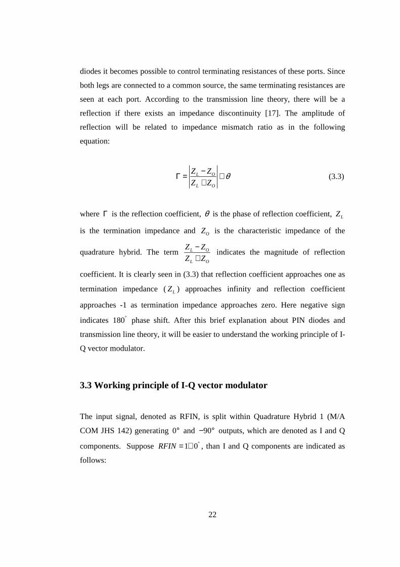
L O
L O
Z Z
Z Zθ−Γ = ∠
+ (3.3)
where Γ is the reflection coefficient, θ is the phase of reflection coefficient, LZ
is the termination impedance and OZ is the characteristic impedance of the
quadrature hybrid. The term L O
L O
Z Z
Z Z
−+
indicates the magnitude of reflection
coefficient. It is clearly seen in (3.3) that reflection coefficient approaches one as
termination impedance (LZ ) approaches infinity and reflection coefficient
approaches -1 as termination impedance approaches zero. Here negative sign
indicates 180° phase shift. After this brief explanation about PIN diodes and
transmission line theory, it will be easier to understand the working principle of I-
Q vector modulator.
3.3 Working principle of I-Q vector modulator
The input signal, denoted as RFIN, is split within Quadrature Hybrid 1 (M/A
COM JHS 142) generating 0° and 90− ° outputs, which are denoted as I and Q
components. Suppose 1 0RFIN °= ∠ , than I and Q components are indicated as
follows:

23
1
2
0.707 0
0.707 90a
a
v
v
°
°
= ∠
= ∠ (3.4)
As shown in Figure 3.2, 0°output of the Quadrature Hybrid 1 becomes input of
Quadrature Hybrid 2(M/A COM JHS 142). This input is also split within
Quadrature Hybrid 2 into two portions. First portion is directed into 0° phase
port of Quadrature Hybrid 2, second portion is directed into 90− ° phase port. The
second portion is delayed 90° in phase relative to the first portion, as it was in
Quadrature Hybrid 1. Part of each portion directed to each phase port is reflected
back. Amplitude and phase of reflected parts depend on the terminating
impedance of the each phase port, which are adjusted by tuning the bias current
of the PIN diodes. Since both phase ports of the quadrature hybrid are terminated
with PIN diodes connected to common source, termination impedances of both
phase ports are equal.
When the PIN diodes are supplied by minimum bias current, PIN diodes acts as
an extremely high terminating resistance, thus reflection coefficient approaches 1.
Namely the first and the second portions of the input signal are reflected back
into the Quadrature Hybrid 2 totally from the phase ports. The first portion is
split into two equal signal components, when it is reflected back from 0° phase
port. The first component is directed into input port, the second component is
directed into output port of Quadrature Hybrid 2. The second component is
delayed 90° in phase relative to the first component. The second part of the input
signal which was directed to the 90°− phase port of the Quadrature Hybrid 2 is
also reflected back to Quadrature Hybrid 2. It is also split into two equal
components. The first component is directed into input port, and the second
component is directed into output port of the Quadrature Coupler 2.
Therefore, the first component reflected from 90° phase port arrives at input port
delayed twice by 90° relative to the first component arriving this port from

24
0° phase port after reflection. So these signals cancel each other. The second
components reflected from 0° and 90°− phase ports arrives output port of the
Quadrature Hybrid 2. These signals are in phase since each has been delayed
once by 90° . So these components are added. This means that, in case of
extremely high terminating resistance, half of the signal received at the input port
of the Quadrature Hybrid 2 arrives to the output port with a 90° phase shift
relative to the received signal. For explaining with mathematical expressions,
denote 0gΓ = ∠ ° in short [5], then
Case 1:
If 1 50R ⟩ Ω then 0g °Γ = ∠
Signal at output port of Quadrature Hybrid 2
( )1 12* .(0.707* *0.707) ( 90 )b av v g= ∠ − ° (3.5)
Signal at isolation port of Quadrature Hybrid 2
( )1 1 .(0.707* *0.707) *(1 0 1 180 )iso av v g= ∠ ° + ∠ ° (3.6)
Case 2:
If 1 50R ⟨ Ω then 180g °Γ = ∠
Signal at output port of Quadrature Hybrid 2
( )1 12* .(0.707* *0.707) (90 )b av v g= ∠ ° (3.7)
Signal at isolation port of Quadrature Hybrid 2
( )1 1 .(0.707* *0.707) *(1 180 1 0 )iso av v g= ∠ ° + ∠ ° (3.8)
Case 3:
If 50R = Ω then 0Γ =

25
1 1 0b isov v= = (3.9)
When the phase ports of the Quadrature Hybrid 2 are terminated with a low
resistance by biasing the PIN diodes with maximum current, instead of
terminating with a high resistance, reflection coefficient at those ports approaches
-1. Namely the signals arriving 0° and 90°− phase ports are reflected back into
Quadrature Hybrid 2, 180° out of phase. As in the case of high resistive
termination, the signals reflected back from 0° and 90°− phase ports cancels each
other at the input port of the Quadrature Hybrid 2, and the signals reflected back
from 0° and 90°− phase ports are in phase so they are added constructively at the
output port of the Quadrature Hybrid 2. Half of the input signal is lost due to the
cancellation process at input port but rest of the signal arrives the output port of
the Quadrature Hybrid 2, however the phase of the output signal becomes shifted
180° relative to the case of high resistive termination. Namely in the case of low
resistive termination, the output signal is 90°− out of phase relative to the
received signal.
Changing bias currents of the PIN diodes between minimum and maximum
currents levels, changes the phase of output signal between 0° and 180° . In the
case of perfect match, when PIN diodes are biased with proper current to obtain
50Ω termination resistance, the reflection coefficient becomes zero; whole of the
signal is directed to load. So it is understood that when the bias currents are
adjusted to obtain a termination resistance between minimum and50Ω , reflection
coefficient varies between -1 and 0. Consequently the magnitude of the signal at
the output port varies between zero and 50% of its maximum value at 180° phase
state. When the bias currents are adjusted to obtain a termination resistance
between 50Ω and maximum, reflection coefficient varies between 0 and 1.
Consequently the magnitude of the signal at the output port varies between zero
and 50% of its magnitude, at the 0° phase state.

26
The Hybrid Coupler 3(M/A COM JHS 142) operates in a similar manner. The
signal at the output port of the Quadrature Hybrid 3 varies between zero and 50
percent of its maximum at 0° phase state or at 180° phase state according to the
signal at the input port of the Quadrature Hybrid 3 depending on the bias currents
of the PIN diodes. For the Quadrature Hybrid 3 there is only one difference. The
signal at the input port of the Quadrature Hybrid 3 is 90° apart from the signal at
the input port of the Quadrature Hybrid 2, thus denoted as Q component of the
modulator.
Since the bias currents of the PIN diodes at I and Q arms are separated, it is
possible to apply different attenuations and obtain different phase states at these
arms. The output signals of Quadrature Hybrid 2 and 3 are vectors with variable
amplitudes but on I and Q axis respectively.
As the final stage of the modulation process the output signals of the Quadrature
Hybrid 2 and 3 are fed into an in-phase power combiner (M/A COM DSS113).
Vector combination of these I and Q signals gives the modulated signal, and it is
provided to the load.
Here it will be suitable to express the output signal with mathematical
expressions for different values of 1R and 2R :
First it is necessary to indicate that summing the vectors a and b at a power
combiner can be expressed as follows:
0.707*( )V a b= + (3.10)
Case 1:
If 1 50R ⟩ Ω and 2 50R ⟩ Ω

27
2 10.707*( 0.707* (0.707* ))OUTRF g j g= − − (3.11)
2 2 1 11 2
2
0.5* tanOUT
gRF g g
g− −= + ∠ −
(3.12)
Case 2:
If 1 50R ⟨ Ω and 2 50R ⟩ Ω
2 10.707*( 0.707* (0.707* ))OUTRF g j g= − + (3.13)
2 2 1 11 2
2
0.5* tanOUT
gRF g g
g−
= + ∠ − (3.14)
Case 3:
If 1 50R ⟩ Ω and 2 50R ⟨ Ω
2 10.707*(0.707* (0.707* ))OUTRF g j g= − (3.15)
2 2 1 11 2
2
0.5* tanOUT
gRF g g
g− −= + ∠
(3.16)
Case 4:
If 1 50R ⟨ Ω and 2 50R ⟨ Ω
2 10.707*(0.707* (0.707* ))oUTRF g j g= + (3.17)
2 2 1 11 2
2
0.5* tanOUT
gRF g g
g−
= + ∠
(3.18)
Where 1g and 2g represent real parts of reflection coefficients at I and Q arms.

28
3.4 Simulations of I-Q vector modulator circuit
For better understanding of working principle of an I-Q vector modulator, ADS
simulations of the circuit given in Figure 3.3 are done. An I-Q vector modulator
circuit is set up by using ideal quadrature hybrids and power combiner.
The simulation circuit is given in Figure 3.5. As the termination impedances of
quadrature hybrids, ideal resistive loads are used.
Figure 3.5 Vector modulator simulation circuit with ideal resistive loads.
Sweeping the values of these resistive loads on each arm of the vector modulator
changes the vector location of the output signal. As it is indicated before in an
ideal case, if the load resistance changes between zero and infinite, reflection
coefficient changes between -1 and 1. Half of the signals at the input of the
quadrature hybrids reach to power combiner which means the modulated signal
can be moved to any point desired on the Smith Chart within 0.7 radius.

29
Figure 3.6 Simulation of I-Q vector modulator circuit with termination resistance tuned between values very close to zero and infinity, at 400 MHz.
If the values of the resistive loads are restricted, the area covered on the Smith
Chart is also restricted, if the values of the resistive loads are asymmetric
around50Ω , the area covered on the Smith Chart becomes asymmetric around
origin. The simulation results about mentioned situations are given in Figure 3.6,
Figure 3.7 and Figure 3.8.
Figure 3.7 Case of asymmetric termination resistance at 400 MHz

30
Figure 3.8 Case of restricted termination resistance at 400 MHz
Using PIN diodes instead of ideal resistive loads also affects the modulation due
to the capacitive and inductive components in PIN diode model. If the ideal load
in simulation circuit is replaced with model including reactive components, the
area covered on Smith Chart is deformed and rotated according to the case of
ideal termination resistaces. The circuit and the results are given in Figure 3.9 and
Figure 3.10.

31
Figure 3.9 I-Q vector modulator circuit with PIN diode model
Figure 3.10 Simulation results for I-Q vector modulator circuit with PIN diode model at 400 MHz

32
3.5 Determination of bias currents of PIN diodes
As it is evidently seen in the simulation results, resistive terminations at the
outputs of the Quadrature Hybrids 2 and 3 affect the performance of I-Q vector
modulator significantly. For proper modulation performance, these impedances
must be defined. Thus the choice of PIN diode is very important. There are some
characteristics to be considered. First the range of series resistance that PIN diode
represents in its forward bias condition becomes major property to be considered.
This resistance should change in a range between values small enough to obtain
reflection coefficient close to -1 and great enough to obtain reflection coefficient
close to 1 while changing bias current in an acceptable range [15]. Second,
resolution of the resistance according to bias current is considered. Because
during the modulation process fine tuning of series resistance is crucial for
convincing performance. Additionally parasitic components of PIN diode come
into question. As it is obviously seen in simulation results parasitic components
of PIN diode affects the area covered on Smith Chart degrading the performance
of I-O vector modulator. Considering these characteristics a PIN diode, Chelton
DH40144, is chosen as termination component of Quadrature Hybrid 2 and 3.
3.6 Implementation of I-Q vector modulator
To verify represented theoretical background and simulation results, it is time for
implementing I-Q vector modulator circuit. First of all the circuit schematics is
prepared. The schematic is given in Figure 3.11.

33
Figure 3.11 I-Q vector modulator schematics
Here C1, C2, C7 and C8 are used as DC blocking capacitors; others are used as
by-pass capacitors. L1, L2, L3, L4, L5, L6 are used as choke inductors. Resistors
are used to complete the circuit of bias currents of the PIN diodes. Vin and Vq are
bias points of PIN diodes for I and Q arms respectively. A single layer printed
circuit board of 1mm thickness is prepared.
Here the marked components are DH40144 which contain two PIN diodes in one
package.
PIN diodes are biased to obtain minimum and maximum equivalent resistances,
also the need for symmetric reflection coefficients around zero is considered. The
resultant bias current necessary for maximum equivalent resistance is determined
as 50 uA and bias current necessary for minimum equivalent resistance is
determined as 50mA for each PIN diode. Since the goal is designing a broadband
V/UHF I-Q vector modulator, measurements are done at 200 MHz, 300 MHz and
400 Mhz. At each frequency bias currents of the PIN diodes are swept between

34
minimum and maximum values, and S21 of I-Q vector modulator is measured
with vector network analyzer for each point.
Figure 3.12 Printed circuit board of I-Q vector modulator
To simplify the process, 8 different bias current is determined within 50 uA and
50 mA range. Bias current is swept from minimum to maximum of these 8 bias
current at one of the I or Q arm while fixing the bias current to one of these 8
values at the other arm. For this measurements a 10K potentiometer is used for
restrict the required bias voltage in an acceptable range. For minimum bias
current levels this series potentiometer is maximized and for maximum bias
current levels this series resistance is minimized to minimize the required bias
voltage level. By this way the maximum required voltage level is restricted to
20V. Measurements are plotted on the I-Q diagrams for each frequency in
following figures.

35
When the results are examined carefully, it is seen that the covered area on Smith
Chart is deformed, and deformation characteristic is frequency dependent. This is
sign of existence of reactive components in PIN diode model as it is mentioned
before. Since this deformation does not degrade the performance of the modulator
dramatically and wideband elimination of these reactive components is hard, we
did not focused on compensation circuits.
Figure 3.13 S21 measurements of I-Q vector modulator for bias currents between 50 uA-50 mA at 200 MHz.

36
Figure 3.14 S21 measurements of I-Q vector modulator for bias currents between 50 uA-50 mA at 300 MHz.
Figure 3.15 S21 measurements of I-Q vector modulator for bias currents between 50 uA-50 mA at 400 MHz.

37
As it is mentioned, at least half of the input signal is dissipated on vector
modulator due to the cancellations. Insertion losses of quadrature hybrids and
other non-ideal components increase the insertion loss of vector modulator. In
this application insertion loss of vector modulator is nearly 4.5 dB over the
bandwidth of operation. As the termination resistances of the quadrature hybrids
get closer to the 50 Ω insertion loss increases.
Figure 3.16 Maximum and minimum insertion losses of I-Q vector modulator
The difference between minimum and maximum insertion loss gives the dynamic
range of vector modulator. This is also a measure of the performance of PIN
diode. If the dynamic range of vector modulator increases, the ability of
modulating the input signal improves.
According to measurements of minimum and maximum insertion loss of vector
modulator, dynamic range of designed I-Q vector modulator is nearly 15 dB as it

38
is seen in Figure 3.16. Since the level of the input signal is in the order of a few
15-20 dBm’s dissipation does not rise temperature considerably.
Vector modulators are employed with other components of a feedforward system,
so input and output matchings of an I-Q vector modulator is also an important
parameter. S11 and S22 of a vector modulator should remain in acceptable limits
within frequency of operation and for different bias conditions. The following
figure shows the S11 and S22 measurements of implemented I-Q vector
modulator, it is also seen that these parameters do not change considerably with
changing bias conditions.
Figure 3.17 S11 and S22 of implemented I-Q vector modulator

39
In the following figure, set-up used for vector modulator measurements is
shown.
Figure 3.18 Set-up used for measurements of vector modulator. Insertion loss of vector modulator is seen on display in case of zero Vin

40
CHAPTER 4
IMPLEMENTATION OF FEEDFORWARD
LINEARIZATION SYSTEM
This chapter introduces the implementation of the feedforward linearization
system. First carrier cancellation loop (CCL) of feedforward system is handled.
Components used in CCL; directional couplers, main amplifier, delay lines and
attenuators, are explained in detail. Measurements of CCL printed circuit board
are discussed. In the second part of this chapter error cancellation loop of the
feedforward system is discussed. Error amplifier is investigated in detail. Results
obtained from the measurements of complete feedforward system printed circuit
board are discussed.
Feedforward linearization system is mainly divided into two parts. First one is
“Carrier Cancellation Loop (CCL)” and second is “Error Cancellation Loop
(ECL)”. In CCL sampled distortion terms are obtained by cancelling the carrier,
in ECL distortion terms are amplified and subtracted from the nonlinear signal to
obtain the amplified carrier in ideal case. The feedforward linearization system is
given with the basic building blocks in Figure 2.2.
4.1 Carrier cancellation loop (CCL)
Carrier cancellation loops is the first loop of feedforward linearization system.
CCL consist of directional couplers, main amplifier, vector modulator and delay

41
line and attenuator if necessary. Block diagram of CCL is given in Figure 4.1. For
better understanding these components will be investigated in detail.
4.1.1 Directional couplers
Directional couplers are used to unequally split the signal flowing in the mainline
and to fully pass the signal flowing in the opposite direction. In an ideal situation
some portion of the signal flowing into port A will appear at Port C. Likewise any
signal flowing into port C will be coupled completely to port A. However ports B
and C and ports A and D are isolated [18]. Any signal flowing into port B will not
appear at port C but will feed through to port A. Likewise any signal flowing to
port A will not appear at port D but will feed through to port B.
Directional couplers used in CCL circuit are realized by two transformers
connected as shown in Figure 4.2. Transformers can be realized on two separate
troids or a binocular ferrite, twin hole ferrite core, can be used to realize both of
the transformers T1 and T2.

42
C1, α1
C1
Feed forward in
C2, α2
C2
gm
Main amplifier
VM1 L1
Delay line C3
C3, α3
CCL Attenuator
Figure 4.1 Block diagram of CCL
Low frequency response of this topology is dictated by the ferrite material
characteristics. High frequency response of this topology is partially governed by
total wire length, since the core effects are no longer dominant near the high
frequency end. Interwinding capacitance, leakage inductance, copper losses and
transformer coupling below unity also degrade high-end performance. Small
shunt capacitances to ground at the coupler ports can be used to improve match
and directivity at the expense of bandwidth [18]. At higher frequencies, lead
length must be kept to a minimum to limit parasitic inductance. To achieve
broadband performance, ground connection lengths must be minimized. High
frequency response improves as core size and wire diameter decrease.

43
Figure 4.2 Directional coupler equivalent circuit
The response of the directional coupler can vary dramatically depending on the
interleaving of the primary and the secondary coils. Insertion loss of this topology
decreases with increasing number of turns due to the choke effects of
transformers. Increasing the number of turns on the primary is limited by the
number of wires that can fit through the core. Also using heavier gauge magnet
wire for the primaries reduces mainline insertion loss and improves power-
handling capability. The isolated port should connect to a good Zo ohm load
impedance, such as a small chip resistor to prevent reflection. Coupling ration of
directional couplers changes by the turn number of transformers, that is;
_ 20 log( )Coupling Ratio N= (4.1)
where turn ratios 1 2N N N= = and 2N ≥ [18]. Here the number of turns is
determined by the number of times that the wire is threaded through the center of
the core even though it may not make a complete 360 degree turn. In this
application turn ratio is chosen as 4 and corresponding coupling ratio is nearly 14
dB. In Figure 4.3 one of the couplers realized with the given topology is seen. A
Micrometals T37-2 core is used for each of the transformers as magnetic material.
This material is chosen considering the frequency range of operation and

44
maximum power applied. An AWG # 24 wire of 0.35 mm thick is used for
windings, and silver coated wires are used as secondary windings of the
transformers. During this application it is observed that the performance of the
couplers is effected by location of the windings, e.g. symmetric or asymmetric.
So all couplers are prepared with similar winding locations to obtain expected
performance. Moreover tightness of the windings affects the coupling ratio. If
windings are not tight enough, coupling ratio changes within band, so it becomes
harder to obtain proper coupling ratio when number of turns decreases. This
affected our design, also it would be easer to realize rest of the feedforward
system(especially error amplifier) by decreasing the coupling ratio, to obtain
constant coupling ratio over bandwidth, a smaller turn number could not be
attained.
Figure 4.3 Directional coupler realized circuit
Another parameter for couplers is directivity which denotes the isolation between
coupling and isolation port. This parameter is not distinctive for our application,
but it is also measured and obtained as better than 13 dB.

45
In CCL circuit 3 couplers are used for two different operations. Couplers C1 and
C2 are used for sampling the signal in their through ports. C1 samples the input
signal before it is fed to the main amplifier. C2 samples the signal amplified by
main amplifier. Coupler C3 is used for subtracting the signals at upper and lower
branches of the CCL. Coupling port of C2 is fed to port B of C3, this signal is
coupled to port D, where port D is through port of C3 for the signal coming from
vector modulator. So these two signals are summed or subtracted if the phases are
180˚ apart.
Since these components are hand-made repeatability of these components affect
the performance of CCL. To examine the repeatability of couplers, all couplers
used for CCL and feedforward printed circuit board are measured. According to
the measured results couplers with 4 turn ratio introduces 0.5 dB insertion loss
throughout bandwidth as seen in Figure 4.4. Coupling ratio is stable within 1 dB
between couplers and stable within 0.4 dB throughout the bandwidth of interest
for each coupler. Results are given in Table 4.1.
Table 4. 1 Insertion loss and coupling ratio measurements of all couplers used in CCL and feedforward printed circuit board.
200 MHz 300 MHz 400 MHz
Coupler IL (dB)
Coupling (dB)
IL (dB)
Coupling (dB)
IL (dB)
Coupling (dB)
CCL C1 -0,38 -15,4 -0,4 -15.7 -0,71 -15.1 CCL C2 -0,37 -15,4 -0,30 -15,3 -0,42 -15,3 CCL C3 -0,35 -15,2 -0,30 -15,2 -0,48 -15,1 FF C1 -0,35 -15,9 -0,38 -16,0 -0,50 -15,8 FF C2 -0,38 -14,6 -0,40 -14,8 -0,74 -14,5 FF C3 -0,40 -15,2 -0,41 -15,4 -0,62 -15,3 FF C4 -0,3 -15,0 -0,28 -15,1 -0,32 -15,2

46
Figure 4.4 Insertion loss of coupler C1 of CCL printed circuit board.
4.1.2 Main amplifier
The amplifier that is desired to be linearized is called the main amplifier. The
feedforward circuitry exists for linearizing the output of this amplifier. Since
there exists a linearization circuit, it is reasonable to operate main amplifier close
to saturation. In the design of the main amplifier one of SEMELAB transistors,
2.5W single ended D2019UK is used. Schematic of designed circuit is given in
Figure 4.5.
In practice gain of an amplifier changes with temperature, frequency, and signal
level. In order to prevent variations due to the temperature and frequency some
circuitry is added while designing main amplifier. Here PT4 is a potentiometer
used for adjusting the gsV of D2019UK, C18 and R16 are used in parallel to
compensate the decreased gain at high frequency, the circuit between R16 and
C14 is used for completing the current flow due to the gsV voltage without any

47
change caused by increase of temperature. Near these precautions C14, R11 and
L7 is used as feedback circuitry of the transistor to ensure the stability of
amplifier and finally 28V_DC is supply of the transistor which is filtered by the
capacitors C15, C16, C17, C21.
Considering CCL block diagram, Figure 4.2, it is possible to calculate the gain of
main amplifier in terms of the parameters of other components. Suppose that
main amplifier has gain mg , couplers have an insertion loss α , coupling ratio c ,
vector modulator and attenuator has insertion losses v and t , respectively. Since
signals reaching the two ports of coupler C3 should be balanced for proper
cancellation [11],
1 2 1 3 1 1 3. . . . . .mg c t c c vα α= (4.2)
1 1 3
1 2 1 3
. .
. . .m
c vg
c t c
αα
= (4.3)

48
Fig
ure
4.5
Sch
emat
ic o
f mai
n am
plifi
er

49
So gain of main amplifier or parameters of other components should be adjusted
to satisfy (4.2). In our implementation c and t are adjusted according to mg . To
find out what the main amplifier introduces to CCL detailed measurements are
done. First of all frequency dependency of gain analyzed, Pin-Pout curve of main
amplifier is obtained for the same dI at different frequencies, obtained curves are
given in Figure 4.6.
Figure 4.6 Pin-Pout curves of D2019UK for the same dI at different frequencies.
Then the dI dependence of gain is analyzed, at 400 MHz Pin-Pout curves are
plotted for different dI values. Results are given in Figure 4.7.

50
Figure 4.7 Pin-Pout curves of D2019UK at 400 MHz for different dI ’s.
Besides, according to the measurements given in Table 4.2, 1dBP of the main
amplifier is close to 30 dBm.
Table 4. 2 Pin Pout values for 100 mA dI at 400 MHz
Pin (dBm) Pout (dBm) Gain (dB)
8,0 23,3 15,3 9,0 24,2 15,2
10,0 25,1 15,1 11,0 26,0 15,0 12,0 26,8 14,8 13,0 27,7 14,7 14,0 28,5 14,5 15,0 29,4 14,4 16,0 30,2 14,2 17,0 30,9 13,9 18,0 31,6 13,6 19,0 32,3 13,3 20,0 33,0 13,0

51
4.1.3 Delay lines and attenuators
Delay lines are used to equalize delays of the upper and lower branches of the
CCL if there exist a delay mismatch. Main amplifier and vector modulator
introduces considerable amount of delays, in the design they are not placed on the
same branch of CCL so fortunately they compensate each other. But in the case
of delay mismatch delay lines must be used in order to not to limit operational
bandwidth. In CCL circuit by-pass capacitors are placed on the upper and the
lower branches, in case of delay mismatch pads of these capacitors might be used
to insert delay lines.
Attenuators are used to match amplitudes of signals arriving to differentiator C3,
if necessary. They are also used to compensate the gain variations of main
amplifier. In our application a 7 dB Π attenuator is placed between C2 and C3 to
equalize the amplitudes of signals subtracted at coupler C3.
4.1.4 Implementation of carrier cancellation loop
CCL loop is implemented as the first part of feedforward system. A printed
circuit card is prepared. Schematic of CCL is given in Figure 4.8. For proper
cancellation of the carrier CCL must also be matched delay wise. If it is
necessary, a delay line can be inserted. To control the delay match of CCL, the
two arms of CCL are measured. Main amplifier arm is measured from input of
CCL to coupling port of C3. Lower arm is measured from input of CCL to input
port of C3. During these measurements it is seen that delay of VM and main
amplifier are affected by the bias conditions significantly. In the case of zero bias
condition, delay of VM increased considerably. This is why measurements are
done under bias conditions. Delay amounts at both arms were comparable
inherently, so there is no need for delay line for CCL. Measured delays of both

52
ports are given in Figure. 4.9. and 4.10. Effects of power level and bias level on
the delay are also measured, any considerable changes obtained.
When amplitude wise match is investigated it is seen that at through port of C3
level of carrier signal coming from upper arm is greater than the carrier signal
coming from VM. Inequalities of signal levels prevent understanding the exact
performance of CCL due to the excessive residual carrier. To equalize amplitudes
of these signals an attenuator of 7 dB is placed between C2 and C3.

53
Fig
ure
4.8
Sch
emat
ics
of C
CL

54
Figure 4.9 Delay of upper arm of CCL from input of C1 to output of C3 when main amplifier biased with 150 mA dI
Figure 4.10 Delay of lower arm of CCL from coupling port of C1 to output of C3 when VM biased with 1 mA inI and qI

55
There is one more problem faced with during the CCL implementation that is
coupling of IMD products to the input of the CCL. Here input output isolation of
main amplifier and directivity of the couplers come into question. Since level of
these IMD products are much smaller than the products coming from the upper
branch, they did not degrade the performance of CCL. It is important to check out
the purity of the carrier signal at the lower arm [19].
After adjusting the delays and amplitudes of the two arms of CCL, carrier
cancellation performance of CCL is measured. Obtained results are given in
Table 4.3
Table 4. 3 CCL output for different frequencies with 0.5 MHz spacing between fundamental tones and 150 mA dI . inI and qI changes between 50
uA and 50 mA for each PIN diode of VM and Pin=16 dBm/tone
Freq(MHz) IMD5(dBm) IMD3(dBm) Fund.1(dBm) Fund.2(dBm) IMD3(dBm) IMD5(dBm)
250 -46,3 -33,3 -41,8 -42,5 -33,5 -47,2
300 -48 -35,5 -43,7 -42,7 -35,5 -47,8
350 -48,5 -37 -51 -49,5 -37,8 -52
400 -53,5 -39 -50,2 -49 -39 -49,8
450 <-55 -42,5 <-55 -53,5 -43 <-55
Table 4. 4 CCL output for different spacing between fundamental tones at 400 MHz with 150 mA dI . inI and qI changes between 50 uA and 50 mA for
each PIN diode of VM and Pin=16 dBm/tone
Spacing(MHz) IMD5(dBm) IMD3(dBm) Fund.1(dBm) Fund.2(dBm) IMD3(dBm) IMD5(dBm)
0.05 -52 -39,5 -46 -47,8 -40 -52
0.25 -48 -35,5 -43,7 -42,7 -35,5 -47,8
0.50 -53,5 -39 -50,2 -49 -39 -49,8
1.00 -53 -39,3 -57,2 -51,5 -39 -54
2.00 -51 -38,2 -50,3 -49,7 -39,3 <-55

56
Table 4. 5 CCL output for different dI ’s at 400 MHz with 0.5 MHz spacing.
inI and qI changes between 50 uA and 50 mA for each PIN diode of VM
and Pin=16 dBm/tone
Id(MHz) IMD5(dBm) IMD3(dBm) Fund.1(dBm) Fund.2(dBm) IMD3(dBm) IMD5(dBm)
100 -52 -39 -46,5 -46 -39,5 -50
150 -53,5 -39 -50,2 -49 -39 -49,8
200 <-55 -39,3 -51 -50 -40,2 <-55
As it is seen in the measurements at CCL output, carrier can be suppressed more
than 10 dB below the IMD products. Such an effective suppression decreases the
peak to average ratio of the signal at the CCL output which is input to the error
amplifier. Namely proper suppression of carrier signal facilitates the design of
error amplifier by decreasing necessary peak power level. Also such an exact
cancellation of carrier can be used to relieve the linearity requirements of the
error amplifier. Further more the success of CCL is directly related with the
performance of VM, which manage nearly 40 dB carrier suppression according to
original signal, this strengths the believe on the attainment of complete
feedforward system.
In Figure 4.11 photograph of the circuit used for CCL measurements is given. As
it is seen the layout of the printed circuit board is prepared in a manner to
minimize the paths which contributed to equalize delays at each branch. The
thickness of the paths on this board are fixed to 60 mil to adjust the impedance of
the paths to 50Ω.
4.2 Error cancellation loop (ECL)
Error cancellation loop is the second loop of the feedforward linearization
system. ECL consists of directional couplers, error amplifier, vector modulator

57
and delay lines and attenuators if necessary. Block diagram of ECL is given in
Figure 4.12. Directional couplers, vector modulator, delay lines and attenuators
are used for the same purpose as in CCL. Differently an error amplifier is placed
in ECL. For better understanding this component will be investigated in detail.
Figure 4.8 Printed circuit board of CCL which is a 1mm thick one layer board.
4.2.1 Error Amplifier
In a feedworfard system, the input signal to the error amplifier consists of
intermodulation and noise from the main amplifier and residual carrier from CCL
where intermodulation term is significant. This signal is amplified by error
amplifier to obtain amplitude wise equal distortion terms at both main amplifier
path and error amplifier path. It is necessary to ensure that the error amplifier
contributes to the intermodulation at the feedforward output as little as possible.
Any intermodulation created by error amplifier, or any leakage signal pick up by

58
the error amplifier, go straight to the feedforward output without any possibility
of cancellation. The intermodulation level of the error amplifier depends upon the
target system linearity and the coupling ratio of C4.
C2, α2
C2
L2
Delay line
C3
C4
C3, α3
C4, α4
Stage 1 Stage 2 Stage 3
VM2
Feed forward out
HMC478MP86 HMC478MP86 D2019UK
ECL
Error amplifier
Main amp. out
CCL out
Attenuator
Figure 4.92 Block diagram of ECL
As it was indicated for gain calculation of main amplifier, gain of error amplifier
also depends on other components in feedforward system. Since signal at the
output of main amplifier reaches to error amplifier through couplers C2 and C3,
also through the attenuator between C2 and C3 and vector modulator, insertion
losses and coupling ratios inserted by these components must be compensated.
Beside this power gain from main amplifier to the feedforward output is
determined by insertion losses of couplers C2 and C4 and delay line if exist.
Since at the output of ECL signals from both main amplifier path and error
amplifier path must have equal intermodulation distortion level, gain of error
amplifier is calculated as follows [11]:
2 2 4 2 1 3 2 4. . . . . . .el c t c v g cα α = (4.4)

59
2 2 4
2 1 3 2 4
. .
. . . .e
lg
c t c v c
α α= (4.5)
where eg is the gain of error amplifier, 2α , 4α are insertion losses of directional
couplers C2 and C4 respectively, 2v is insertion loss of vector modulator on error
amplifier path, 2l is insertion loss of delay line on main amplifier path, 2c , 3c and
4c are coupling ratios of couplers C2, C3 and C4 respectively.
The peak-power requirement of error amplifier is also an important parameter for
implementation of ECL. Peak the average ratio of input signal mainly determines
the need of peak power of error amplifier. If error amplifier does not fulfill the
peak power requirement, input signal can not be amplified linearly. This is why
analyzing the feedforward system before determining the specifications of error
amplifier is crucial.
Suppose that main amplifier is a Class AB amplifier with an average output
power MP , and distortion level MD , then the distortion power at the output of
main amplifier can be approximated as follows;
10.3.10MD
D MP P= (4.6)
The power gain (or loss) between the output of main amplifier and the
feedforward output is determined by the insertion losses of the couplers on this
path and insertion loss of the delay line if there is one. That is
2 2 22 4 2. .lα α (4.7)

60
If the second loop is balanced the gain through error amplifier path and main
amplifier path must be equal. Suppose that EP denotes the average output power
of error amplifier,
2 2 210 102 4 2 2
4
1. 3.10 10 . . . .
CM SD
E MP P lc
α α
= +
(4.8)
Here CS represents the residual carrier power from the CCL. It is clearly seen
that depending the relative performance of the main amplifier and the carrier
suppression, the dominant contribution to the average output power of the error
amplifier can either be distortion power or residual carrier power.
The peak power requirement of error amplifier is higher than the average power
by an amount equal to the peak-to-average ratio of the main amplifier MP∆ , and
an additional margin EB , to ensure linear operation, that is,
1 . .E E E MP P B P= ∆ (4.9)
where 1EP represents the peak power of error amplifier [11]. To minimize
distortion due to the signal clipping peak-to-average ratio of main amplifier is
also adjusted according to peak-to-average ratio of input signal. Peak-to-average
ratio of main amplifier can be expressed as,
1MM
M
PP
P∆ = (4.10)
Substituting MP∆ , peak power of the error amplifier can be expressed in terms of
the peak power of the main amplifier, that is,

61
2 2 210 101 1 2 4 2 2
4
1. . 3.10 10 . . . .
CM SD
E M EP P B lc
α α
= +
(4.11)
(4.11) states that peak power of error amplifier is a function of peak power and
intermodulation performance of main amplifier, the carrier suppression of CCL
coupler and delay line losses and coupling ratio of C4.
Error amplifier is one of the most important components of a feedforward
linearization system. It has a significant effect on the performance of feedforward
system [20]. So it is necessary to design a linear error amplifier to obtain beter
results for IMD cancellation at the output of feedforward linearizer. In this
application we did not focused on designing such a proper error amplifier due to
the lack of time. Instead we focuse on implementing a complete feedforward
system. So ready amplifiers and the main amplifier of CCL is used in cascade
instead.
In our application nearly 45 dB error amplifier gain is needed due to the high
coupling ratios of couplers. To achieve such a high gain a 3 stage error amplifier
is used. For the first two stages a gain block of Hittite HMC478MP86 is used.
The HMC478MP86 is a SiGe Heterojunction Bipolar Transistor (HBT) Gain
Block covering DC to 4 GHz. 1dBP of this gain block is 18 dBm. This Micro-P
packaged amplifier is matched to 50Ω at input and output. The HMC478MP86
offers 22 dB of gain. Needs only a single supply of 5V and a simple bias
circuitry. Bias circuitry is given in Figure 4.13. where value of L1 is frequency
dependent and choosen as 82 nH for this application. C1 and C2 are 1 nF by-pass
capacitors as in the rest of the circuit.
As the third stage of the error amplifier Semelab D2019UK is used as in main
amplifier case with the same topology.
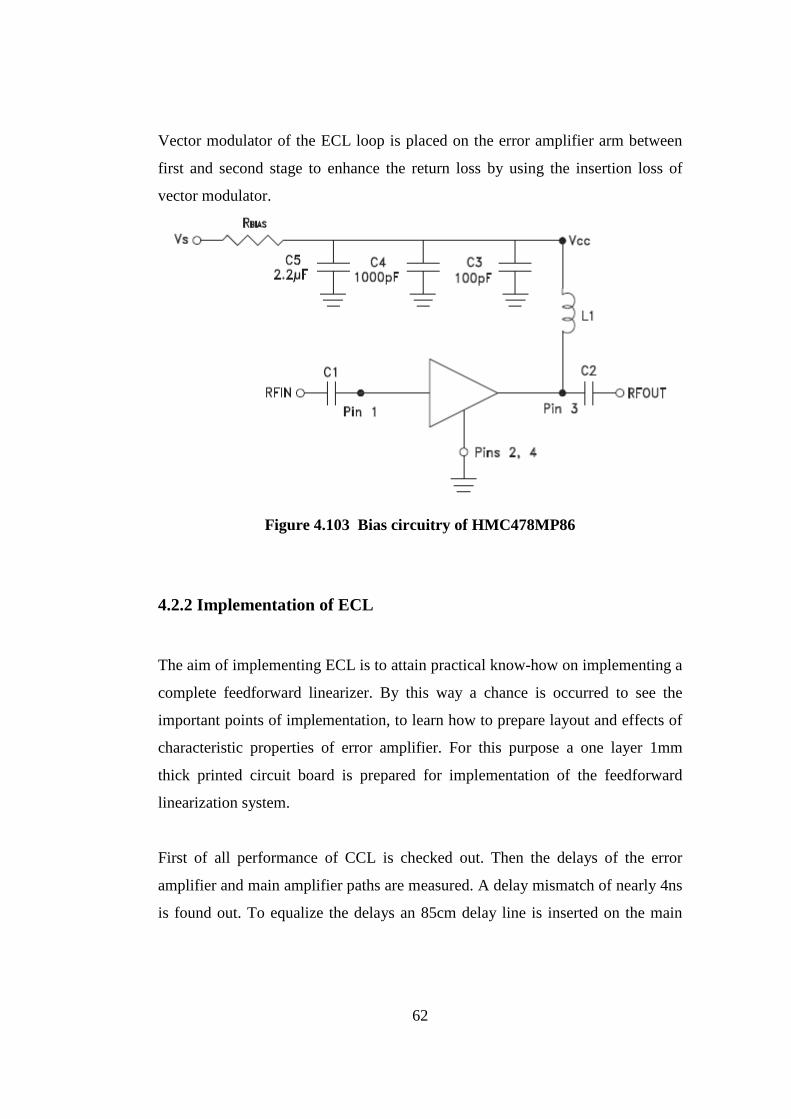
62
Vector modulator of the ECL loop is placed on the error amplifier arm between
first and second stage to enhance the return loss by using the insertion loss of
vector modulator.
Figure 4.103 Bias circuitry of HMC478MP86
4.2.2 Implementation of ECL
The aim of implementing ECL is to attain practical know-how on implementing a
complete feedforward linearizer. By this way a chance is occurred to see the
important points of implementation, to learn how to prepare layout and effects of
characteristic properties of error amplifier. For this purpose a one layer 1mm
thick printed circuit board is prepared for implementation of the feedforward
linearization system.
First of all performance of CCL is checked out. Then the delays of the error
amplifier and main amplifier paths are measured. A delay mismatch of nearly 4ns
is found out. To equalize the delays an 85cm delay line is inserted on the main

63
amplifier path between C2 and C4 couplers. Delay measurements of both paths
are given in following figure
Figure 4.114 Delay measurement of upper and lower arm of ECL
Before examining the performance of the overall system, performances of each
component on ECL is measured. During these measurements it is realized that the
vector modulator on ECL is not working properly. Vector modulator does not
cover all quadrants of Smith Chart, one of the quadrature couplers employed in
vector modulator is deformed. All the feedforward measurements are done by
using this deformed vector modulator. So IMD cancellation performance of
feedforward system is not as good as it is expected but system still offers an
acceptable amount of enhancement on IMD levels. Measured data is given in the
following table.

64
Table 4. 6 Feedforward output for Pin=16 dBm/tone and dI =150 mA
IMD5 IMD3 FUND. 1 FUND. 2 IMD3 IMD5
250 MHz Main Amp. Output -14,2 1,8 28 27,5 3,8 -16
Feedforward Output -20,7 -5,3 27,2 27 -4,3 -25
300 MHz Main Amp. Output -14,5 2,5 27,1 26,5 3 -16,2
Feedforward Output -26 -6,7 24,8 24,5 -5,1 -25,5
400 MHz Main Amp. Output -16,8 0 24,7 24,3 -0,7 -17,8
Feedforward Output -23,2 -8,8 24 23,8 -8,2 -25,3
450 MHz Main Amp. Output -22,5 -1,5 24 23,5 -1,8 -22,5
Feedforward Output -16,7 -18,2 21,7 21,3 -14 -18,5
As it is seen in Table 4.5 at least 7 dB IMD suppression is achieved over 250-450
MHz range. Best performance is obtained at 450 MHz. But 7 dB suppression of
IMD can be life saving for some applications. If performance of CCL (nearly
40dB carrier suppression) is considered, it is clearly seen that performance of the
overall system can be enhanced by replacing the deformed vector modulator with
a properly working one.
4.3 Efficiency of feedforward system
Feedforward system is one of the best linearization system if linearization
performance is considered but it suffers from efficiency. Since there are two
power amplifiers employed to obtain the same power level, overall efficiency of
the system decreases considerably. Furthermore overall performance of the
system depends on linearity of the error amplifier [11]. If efficiency of an
amplifier is described as a measure of how effectively DC power is converted to
RF power, η can be expressed as,
OUT
DC
P
Pη = (4.12)
The total DC power drawn from DC supplies is given as,

65
_ _DC DC M DC EP P P= + (4.13)
The efficiency of main amplifier operating in class AB is a function of average
output power,
_M
DC MM
PP
η= (4.14)
Since the peak to average ratio of main amplifier is defined as 1 /M M MP P P∆ = ,
(4.14) can be rewritten as,
1_ .
MDC M
M M
PP
Pη=
∆ (4.15)
The efficiency of error amplifier can be expressed in term of peak power of this
amplifier,
1 1_ .
E MDC E
E E E
P PP
Pη η= =
∆ (4.16)
Where 1 1/E M EP P P∆ = is the ratio of peak power capabilities of the error and
main amplifiers. Due to the insertion losses of the components on the main
amplifier path before output of the feedforward system, output power of
feedforward system is less than the output power of main amplifier, that is,
2 22 2 4. . .OUT MP P lα α= (4.17)
Substituting these results to (4.12) overall efficiency of a feedforward system is
obtained as follows,
2 2
2 2 4. .
1.
FF
M
M E E
l
P
P
α αη
η η
= ∆+ ∆
(4.18)
According to (4.18), feedforward efficiency is dependent on many factors like

66
insertion losses of couplers and delay lines, efficiency of main amplifier at
maximum average output power, efficiency of error amplifier at peak power and
ratio of main and error amplifiers peak powers. If power consumption of other
components like vector modulators is considered, efficiency of feedforward
system is degraded more.
Efficiency of the implemented circuit is calculated to compare the single main
amplifier case and a complete feedforward linearizer case. As it is expected
efficiency of the overall system is degraded due to the extra power consumption
of additional elements. At 300 MHz the power at main amplifier output is
measured as 1.4 W and 0.23 A is drawn from 28 V. Then DC to RF efficiency of
the main amplifier is calculated as 21.7%, but if external linearization circuitry is
included nearly 0.435 A is drawn from 28 V and 132 mA is drawn from 5 V.
Then overall DC to RF efficiency of the system is calculated as 8%. This can be
summarized as efficiency of the system is decreased from 22% to 8% for nearly
10 dB suppression of IMD. Designer should consider the priorities of the system
If 10 dB suppression of IMD products is life saving, designer might permit
degradation of efficiency in the expence of linearity.
Input and output matching of a feedforward system is one more issue to consider.
Since this system will be inserted in a communication system, it must be matched
to the stages placed just before and after feedforward linearizer. In other words
S11 and S22 of a feedforward system must be better than -10 dB to prevent signal
loss due to the mismatch. In this work couplers C1and C4 are the interfaces of the
system with the other stages. According to the measurements S11 and S22 of the
coupers are better than -10 dB over operation bandwidth, which is an acceptable
matching ratio.
In the following photograph the set-up used for feedforward measurements is
seen.

67
Figure 4.15 Set-up used for feedforward printed circuit board

68
CHAPTER 5
CONCLUSION
In modern communication systems, the need for both linearity and efficiency
increase. Increasing number of users and growing demand for higher data rates
forces communication systems to use modulation schemes having amplitude and
phase modulation at the same time and forcing transmitters supporting
multicarrier and high peak-to-average ratio signals. Due to the nature of
semiconductor, nonlinearity is inherently present, also dealing with nonconstant
envelope and high peak-to-average ratio signals increase the nonlinearity of a
system considerably. In order to decrease nonlinear effects a certain back-off
margin can be guarantied during the design of power amplifier, but this works at
the expense of efficiency and also limits the output power capability. However,
efficiency is also an indispensable parameter for communication systems. Here
employing linearization techniques become reasonable. Linearization techniques
are used to enhance the linearity of a PA which is acceptably efficient.
In this thesis one of the best linearization technique, feedforward linearization is
implemented. First most important component of a feedforward system, an I-Q
vector modulator covering the frequency range of 250-450MHz is designed and
implemented. During implementation of vector modulator, choosing a PIN diode
which is proper for this application is one of the hardest topics. Different PIN
diodes are tested and the one with higher series resistance resolution and
minimum parasitic components is chosen. Since PIN diode is not an ideal
component bias current dependent series resistance of this component does not
changes between zero and infinity. This degrades the performance of vector

69
modulator by limiting the area covered on Smith Chart. Also the parasitic
capacitance and inductance seen in PIN diode model distorts the area covered on
Smith Chart. Compensating these parasitic effects of the PIN diode is tried but
due to the sharp frequency dependency, wideband cancellation could not be
managed. Furthermore during our work we realized that the relation between the
bias current and series resistance should at least be close to being linear for exact
adjustment of the reflection coefficient. Otherwise series resistance changes
rapidly with a slight change in bias current which obstructs fine tuning of
reflection coefficient, namely obstructs catching the exact cancellation point. For
adjusting the bias current two methods are used in cooperation. First inV and Vq
voltages are adjusted on the supplies. Then a multiturn 10KΩ potentiometer is
used to fine tune the bias current by changing the equivalent series resistance
between PIN diode and ground.
I-Q vector modulator inherently inserts at least 3 dB insertion loss due to the
working principles of quadrature hybrids [21] but the vector modulator designed
during this thesis has nearly 4.5 dB insertion loss when bias currents are not
applied. Because PIN diodes’ maximum series resistance is not infinite and the
combiner and the quadrature couplers are not ideal components. While testing the
performance of the vector modulator the points that can be covered on Smith
Chart are identified by measuring S21. The area covered on the Smith Chart must
be symmetric according to the origin and should be wide enough. Symmetry of
the area states the symmetric movement of reflection coefficient between 1 and -1
which allows carrying input signal to the desired quadrant of the Smith Chart.
Width of the area states the insertion loss introduced by vector modulator.
Wideband operation of the vector modulator is mainly dependent on the
frequency range of the quadrature couplers and power combiner [22]. Choosing
convenient components supported wideband operation of designed vector
modulator, thus satisfactory results are obtained between 200-450 MHz range.

70
As second step of this thesis carrier cancellation loop of a feedforward system is
implemented by using the designed I-Q vector modulator. Here the aim was to
ensure the performance of designed I-Q vector modulator and to obtain practical
know-how about implementation of linearization circuits. A printed circuit board
is prepared for this purpose. A 30-512 MHz amplifier, designed by using
Semelab D2019UK, is used as main amplifier. The characteristic of main
amplifier is analyzed in terms of gain, IMD and frequency dependency. Then the
two branches of CCL should be amplitude and delay matched. If these conditions
are not satisfied, performance of the vector modulator and carrier cancellation
loop will most probably be evaluated wrong [23]. To equalize the delays of both
arms of CCL, vector modulator and main amplifier are placed on different arms
of CCL, since these components have dominant effect on delay. If there exists a
delay mismatch it is impossible to compensate this with vector modulator, as
vector modulator works only for phase and amplitude matching. But also it is not
possible to match amplitudes of carriers by using vector modulator if the carrier
level coming to the C3 from upper arm of CCL is higher than it is on vector
modulator arm. If carrier level is higher on the upper arm than it is on the lower
arm, there will not be exact cancellation of carrier anytime. So during
implementation of CCL signal levels must be controlled for each step. Also
sampling a pure carrier at the input of the CCL is another crucial point during
CCL implementation. If this sampled carrier at coupling port of C1 is not clear
then cancellation will get harder. In this work a main amplifier with feedback
circuit is used. This caused coupling of IMD products to the input of main
amplifier and and also to the lower arm of CCL where a pure carrier is needed.
Levels of these distortion products was too weak to affect the performance of
CCL, but this is a notification to think more on input-output isolation of main
amplifier and directivity of C1.
According to the measurements carried out during this thesis, CCL suppresses the
carrier nearly by 10 dB below the IMD products in 250-450 MHz range. 10 dB

71
suppression is enough to ensure that the IMD products drive the error amplifier of
ECL. Such a good suppression decreases the peak-to-average ratio of the signal at
the output of CCL so the signal can be accepted as a two tone signal.
Performance of CCL is tested for different input signal levels. Changing input
signal level changes phase and amplitude characteristics of the amplifier so it is
necessary to adjust a new bias condition for proper cancellation. Changing the
spacing between the tones of input signal, namely changing the bandwidth of the
input signal, also has similar effect. There is one more situation that is faced with
is that performance of CCL is also relatively dependent on the temperature
changes. If amplifier is cooled down without changing bias conditions of vector
modulator, carrier cancellation performance is degraded. So to enhance the
overall performance, bias conditions of vector modulator must be adjusted if any
parameter of CCL system changes. This is why there should be a self control
mechanism for bias conditions of vector modulator rather than manual control.
As last step of this work, a complete feedforward system is implemented. An
error amplifier is employed in ECL to amplify the distortion term. Error amplifier
must amplify the output of CCL to a level where distortion term becomes
comperable at the output of feedforward system. Error amplifier must be
designed as linear as possible to prevent adding extra distortion terms to the CCL
output. Any distortion produced by the error amplifier directly reaches to the
output of feedforward system. Gain of error amplifier must compensate the losses
inserted by vector modulator and couplers. So decreasing the coupling ratio of
couplers simplify the design of the error amplifier. Error amplifiers must be
operated with a back-off margin enough for linear operation and possible increase
of peak-to-average ratio of input signal. In this thesis error amplifier design is not
considered in detail, due to the lack of time. Simply a three stage error amplifier
is designed. A MMIC amplifier of Hittite HMC478MP86 is used in cascade as
the first two stages, and Semelab D2019UK is used as the third stage. A 47 dB of
gain is achieved on the error amplifier. Since error amplifier and vector

72
modulator are placed on the same arm of ECL, lower and upper arms are not
delay matched as it is in CCL case. So an 85 cm delay line is inserted to upper
arm.
During the ECL measurements it is realized that the second vector modulator of
the feedforward system employed with the phase and amplitude matching of error
cancellation loop is not working adequately due to the distorted quadrature
couplers. So wideband cancellation process could not be achieved properly in
error cancellation loop as good as it is in CCL. However, at 450 MHz IMD
products at the output of feedforward system are suppressed nearly by 15 dB.
According to the measurements at 400 MHz it is seen that, biasing conditions of
both vector modulators are dependent on frequency, bandwidth and power level
of the input signal.
As well as other feedforward studies, feedforward linearization system suffers
from efficiency. Requiring a second amplifier to obtain the same power level
decreases the efficiency of the system significantly. But it is seen that by
improving the carrier suppression performance of CCL, linearity requirement of
error amplifier can be loosen, and by this way overall efficiency of the
feedforward system can be increased.
Another handicap of the feedforward system is the difficulty of integrating this
external circuitry to a real system. At least five additional supply voltages are
needed for vector modulators and error amplifier. Also adjusting the bias voltages
of vector modulators is a separate research area on its own.
As a further work, a self control scheme for feedforward system can be developed
to obtain a more compact and realizable linearization system. For example a
feedback mechanism controlling the performance of feedforward output which
adjusts the bias levels by using a look-up table can be developed. Another subject

73
of research may be implementing a hybrid system combining both feedforward
and predistortion linearization systems to improve the poor efficiency of
feedforward system without discarding the superior wideband operation and high
linearization performance of this system.

74
REFERENCES
[1] N. Pothecary, “Feedforward Linear Power Amplifiers”, Artech House,
1999.
[2] S. Myoung, “Low Frequency Feedforward and Predistortion Linearization
of RF Power Amplifiers”, PhD thesis, The Ohio State University, 2006.
[3] A. H. Coşkun, “Stochastic Characterization and Mathematical Analysis of
Feedforward Linearizers”, PhD thesis, The Middle East Technical
University, September 2003.
[4] S. C. Cripps, “Advanced Techniques in RF Power Amplifier Design”,
Artech House, 2002.
[5] An Application Note for VM-MCM-1.9G [Online], Available:
http://www.merrimacind.com, 17 Jan 2010.
[6] S. A. Maas, “Nonlinear Microwave and RF Circuits”, Artech House,
1988.
[7] P. Kenington, “High Linearity RF Amplifier Design”, Artech House,
2000.
[8] A. Mutlu, “Multi-Tone Representation of Arbitrary Waveforms and
Application to the Analysis of Nonlinear amplifiers and Feedforward
Linearizers”, M.Sc. thesis, The Middle East Technical University, August
2005.

75
[9] J. A. Cherry, “Distortion Analysis of Weakly Nonlinear Filters Using
Volterra Series”, PhD. thesis submitted by Carleton University, December
1994.
[10] H. Tang, “Educational Testbed Design for Baseband Predistortion
Linearization of RF Power Amplifiers”, M.Sc. thesis, The Ohio State
University, 2008.
[11] J. Voulevi and T. Rahkonen, “Distortion in RF Power Amplifiers”, Artech
House, 2003.
[12] P. B. Kensington and D. W. Bennett, “Linear Distortion Correction Using
a Feedforward System”, IEEE Transaction on Vehicular Technology, vol.
45, no. 1, pp. 74-81, Feb 1996.
[13] D. Pennington, “Dynamic Range Improvements in Radar Systems using
Transmitter Linearization”, 1st EMRS DTC Technical Conference, p C15,
Edinburgh, 2004.
[14] A. Ünlü, Ş. Demir, “200-400 MHz I-Q Vector Modulatör Tasarımı ve
Üretimi”, URSI Ulusal Ulusal Kongresi 2008, pp. 93-95, Antalya, 2008.
[15] PIN Diode Vector Modulators - Fundemantals and Drive Requirements
[Online], Available: http://www.macom.com.tr, 17 Jan 2010.
[16] The PIN Diode Circuit Designers Handbook [Online], Available:
http://www.ieee.li/pdf/pin_diode_handbook.pdf, 17.Jan 2010.
[17] R. E. Collin, “Fundamentals for Microwave Engineering”, Mc Graw-Hill
International Editions Electrical Engineering Series, 1992.

76
[18] RF Directional Couplers [Online], Available:
http://michaelgellis.tripod.com, 17 Jan 2010.
[19] S. C. Cripps, “RF Power Amplifiers for Wireless Communications”,
Artech House, 1999.
[20] L. Silverman and C. Del Plato, “Vector Modulators Enhance Feedforward
Cancellation”, Microwaves and RF Magazine, pp.52-56, March 2008.
[21] Phase Shifters, Vector Modulators, Delay Lines and Frequency Translator
Applications [Online], Available: http://www.gtmicrowave.com, 17 Jan
2010.
[22] Broadband I-Q Vector Modulator Demonstrates the Leading Edge in
Performance [Online], Available: http://www.gtmicrowave.com, 17 Jan
2010.
[23] K. J. Parsons and P. B. Kenington, “Effect of Delay Mismatch on a
Feedforward Amplifier”, IEE Proceedings-G, vol. 139, no. 5, pp.591-593,
1992.
[24] B. J. Harker, “Dynamic Range Enhancements in Radar Systems”, 2nd
EMRS DTC Technical Conference, p A10, Edinburgh, 2005.
[25] R. J. Wilkinson and P. B. Kenington, “Specifications of Error Amplifiers
for use in Feedforward Transmitters”, IEEE Proceedings on Circuits,
Devices ans Systems, vol. 139, no. 4, pp.477-480, August 1992.

77