Design and FPGA Implementation of an OFDM … and FPGA Implementation of an OFDM System Based on...
119
Design and FPGA Implementation of an OFDM System Based on 3GPP LTE Standard over Multipath Fading Channel Ahmed Almajdoob A Thesis In The Department of Electrical and Computer Engineering Presented in Partial Fulfillment of the Requirements For the Degree of Master of Applied Science at Concordia University Montréal, Québec, Canada November 2012 ©Ahmed Almajdoob, 2012
Transcript of Design and FPGA Implementation of an OFDM … and FPGA Implementation of an OFDM System Based on...

Design and FPGA Implementation of an OFDM System Based on
3GPP LTE Standard over Multipath Fading Channel
Ahmed Almajdoob
A Thesis
In
The Department
of
Electrical and Computer Engineering
Presented in Partial Fulfillment of the Requirements
For the Degree of Master of Applied Science at
Concordia University
Montréal, Québec, Canada
November 2012
©Ahmed Almajdoob, 2012

CONCORDIA UNIVERSITY
SCHOOL OF GRADUATE STUDIES
This is to certify that the thesis prepared By: Ahmed Almajdoob Entitled: “Design and FPGA Implementation of an OFDM System Based on
3GPP LTE Standard over Multipath Fading Channel” and submitted in partial fulfillment of the requirements for the degree of
Master of Applied Science Complies with the regulations of this University and meets the accepted standards with respect to originality and quality. Signed by the final examining committee: ________________________________________________ Chair Dr. R. Raut ________________________________________________ Examiner, External Dr. I. Hassan (MIE) To the Program ________________________________________________ Examiner Dr. A. K. Elhakeem ________________________________________________ Supervisor Dr. Y. R. Shayan Approved by: ___________________________________________ Dr. W. E. Lynch, Chair Department of Electrical and Computer Engineering ____________20_____ ___________________________________ Dr. Robin A. L. Drew Dean, Faculty of Engineering and Computer Science

iii
ABSTRACT
Design and FPGA implementation of an OFDM System Based on
3GPP LTE Standard over Multipath Fading
Ahmed Almajdoob
Orthogonal Frequency Division Multiplexing (OFDM) is an appealing multi-carrier modulation
technique for achieving high-data-rate transmission over multipath fading channel. Due to the set
of orthogonal subcarriers and time interval between symbols, OFDM provides high bandwidth
efficiency and robustness against Intersymbol Interference (ISI). By applying OFDM, several
requirements of standards for advanced communications systems can be fulfilled leading to wide
adoption and utilization commonly used in wireless systems. Field programmable gate arrays
(FPGAs) offer high-performance and low-cost DSP solution for digital communication system
implementation and verification. Due to their flexibility and upgradeability, FPGAs have become
widely used in implementation of DSP functions
In this thesis, an OFDM system is designed and implemented on an FPGA platform in
accordance with the design flow methodology. Based on 3rd Generation Partnership Project
(3GPP) Long Term Evolution (LTE) parameters, extended and normal-CP OFDM systems are
modeled and simulated in MATLAB to examine the systems using BER performance. The
OFDM system with extended-CP has been selected for the design because of its better robustness
against wireless Rayleigh multipath fading channels. The extended-CP OFDM system is
transformed to a Simulink model and analyzed.
iv
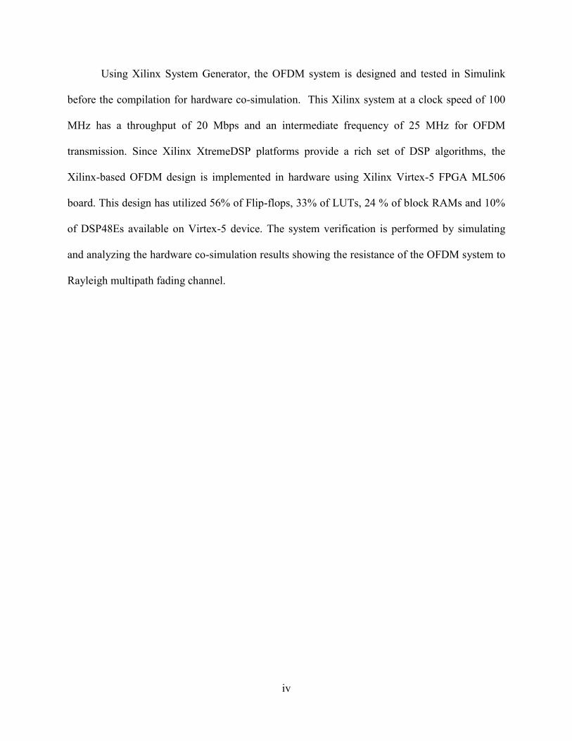
Using Xilinx System Generator, the OFDM system is designed and tested in Simulink
before the compilation for hardware co-simulation. This Xilinx system at a clock speed of 100
MHz has a throughput of 20 Mbps and an intermediate frequency of 25 MHz for OFDM
transmission. Since Xilinx XtremeDSP platforms provide a rich set of DSP algorithms, the
Xilinx-based OFDM design is implemented in hardware using Xilinx Virtex-5 FPGA ML506
board. This design has utilized 56% of Flip-flops, 33% of LUTs, 24 % of block RAMs and 10%
of DSP48Es available on Virtex-5 device. The system verification is performed by simulating
and analyzing the hardware co-simulation results showing the resistance of the OFDM system to
Rayleigh multipath fading channel.

v
Acknowledgements
The success of any project depends largely on the guidance and encouragement of many people.
This thesis would not have been possible without their support. Therefore, I take this opportunity
to express my sincere gratitude to my supervisor, Dr. Yousef R. Shayan, for his unwavering
support, enthusiastic supervision and invaluable assistance with the development and completion
of this research. He has shared his technical expertise and guided me diligently in the arduous
process of thesis writing. His availability and patience have proven a great inspiration to me
throughout my master’s studies at Concordia University.
I also wish to express my deep gratitude and love to my beloved parents for their
understanding and enormous support through the duration of my studies. Their consistent
encouragement has motivated and guided me on the path towards my degree completion.
Last but not the least, I am deeply indebted to my friends and colleagues who have
helped me adapt to a new life in a foreign country and provided the moral support needed for the
fulfillment of my academic goals.
vi
Table of Contents
List of Figures ............................................................................................................................... ix
List of Tables ................................................................................................................................ xi
List of Acronyms ......................................................................................................................... xii
Chapter 1 Introduction…………. .............................................................................................. 1
1.1 Background ........................................................................................................................... 1
1.2 OFDM History and Development ......................................................................................... 2
1.3 Thesis Motivation and Contribution ..................................................................................... 4
1.4 Thesis Organization............................................................................................................... 7
Chapter 2 OFDM System and Wireless Channel ..................................................................... 9
2.1 Introduction to OFDM Modulation ....................................................................................... 9
2.2 QPSK Baseband Modulation .............................................................................................. 11
2.3 Overview of OFDM System ............................................................................................... 13
2.3.1 Guard Interval and Cyclic Prefix .................................................................................. 16
2.3.2 Pulse Shaping ............................................................................................................... 17
2.3.3 Peak to Average Power Ratio ....................................................................................... 19
2.4 Wireless Fading Channel .................................................................................................... 20
2.4.1 Small-Scale Fading Channel ........................................................................................ 20
2.4.2 Frequency Dispersion ................................................................................................... 22
2.4.3 Time Dispersion ........................................................................................................... 24
2.4.4 Impulse Response of Fading Channel .......................................................................... 25
2.5 LTE Physical Layer Downlink Parameters ......................................................................... 26
2.6 Summary ............................................................................................................................. 28
Chapter 3 OFDM System Design and Simulation .................................................................. 30

vii
3.1 Design Flow ........................................................................................................................ 30
3.2 Floating-Point Modeling and Simulation in MATLAB ...................................................... 33
3.2.1 Random Data Generation ............................................................................................. 34
3.2.2 QPSK Modulation ........................................................................................................ 35
3.2.3 Serial to Parallel Conversion ........................................................................................ 36
3.2.4 Zero Padding ................................................................................................................ 37
3.2.5 Inverse Discrete Fourier Transformer .......................................................................... 38
3.2.6 Adding Cyclic Prefix .................................................................................................... 38
3.3 Channel Modeling ............................................................................................................... 39
3.4 MATLAB Simulation Results ............................................................................................. 45
Experiment 1: The Effect of Flat Fading Channel ................................................................ 45
Experiment 2: The Effect of 30-Path Channel ...................................................................... 47
Experiment 3: The Effect of 100-Path Channel .................................................................... 48
Experiment 4: The Effect of 140-Path Channel .................................................................... 49
3.5 Floating-Point Modeling and Simulation in Simulink ........................................................ 50
3.6 Simulink Simulation Results ............................................................................................... 52
3.7 Summary ............................................................................................................................. 53
Chapter 4 OFDM Hardware Design and FPGA Implementation ......................................... 55
4.1 Xilinx OFDM Transmitter .................................................................................................. 56
4.1.1 Random Data Generation ............................................................................................. 57
4.1.2 QPSK Modulation ........................................................................................................ 58
4.1.3 Zero-Padding ................................................................................................................ 59
4.1.4 OFDM Modulation ....................................................................................................... 60
4.1.5 Digital Up-Conversion ................................................................................................. 66
4.2 Rayleigh Fading Channel .................................................................................................... 68

viii
4.3 AWGN Channel .................................................................................................................. 72
4.4 Xilinx OFDM Receiver ....................................................................................................... 73
4.4.1 Down-Conversion and OFDM Demodulation ............................................................. 74
4.4.2 Phase Noise Cancellation ............................................................................................. 75
4.4.3 Puncturing ..................................................................................................................... 79
4.4.3 QPSK Demodulation .................................................................................................... 80
4.5 Summary ............................................................................................................................. 81
Chapter 5 Hardware Verification and Test Results ............................................................... 82
5.1 The Simulation Results of Xilinx OFDM System .............................................................. 82
5.2 Hardware Co-Simulation .................................................................................................... 85
5.2.1 Introduction of XtremeDSP board ................................................................................ 86
5.2.2 Hardware Co-Simulation Setup .................................................................................... 89
5.3 Hardware Co-Simulation Results ........................................................................................ 92
5.4 Hardware Utilization ........................................................................................................... 94
5.5 Summary ............................................................................................................................. 97
Chapter 6 Conclusion and Future Work ................................................................................. 98
Bibliography .............................................................................................................................. 101

ix
List of Figures
Figure 2-1: Bandwidth comparison between FDM and OFDM ................................................... 10
Figure 2-2: QPSK signal constellation ......................................................................................... 12
Figure 2-3: OFDM frequency spectrum ....................................................................................... 15
Figure 2-4: OFDM cyclic prefix ................................................................................................... 17
Figure 2-5: OFDM Power spectrum density for different N subcarriers ...................................... 18
Figure 2-6: Multipath fading ......................................................................................................... 21
Figure 2-7: Doppler effect on a mobile station ............................................................................. 23
Figure 2-8: Flat and frequency-selective fading ........................................................................... 25
Figure 2-9: Radio frame structure type 1 ...................................................................................... 27
Figure 3-1: Implementation design flow ....................................................................................... 31
Figure 3-2: Block diagram of an OFDM transceiver .................................................................... 34
Figure 3-3: Exponential and 2-ray models .................................................................................... 42
Figure 3-4: BER of the OFDM systems under flat fading channel .............................................. 46
Figure 3-5: BER of the OFDM systems under 30-path channel ................................................... 47
Figure 3-6: BER of the OFDM systems under 100-path channel ................................................. 48
Figure 3-7: BER of the OFDM systems under 140-path channel ................................................. 49
Figure 3-8: QPSK-OFDM model in Simulink .............................................................................. 51
Figure 3-9: BER of the QPSK-OFDM system under AWGN channel ........................................ 53
Figure 4-1: Block diagram of Xilinx OFDM transmitter.............................................................. 56
Figure 4-2: Xilinx QPSK modulator ............................................................................................. 58
Figure 4-3: Xilinx Zero-padding design ....................................................................................... 59

x
Figure 4-4: Xilinx FFT V7.1 block with unscaled output ............................................................ 62
Figure 4-5: Pipelined Stream I/O Architecture ............................................................................. 63
Figure 4-6: Xilinx OFDM modulator design ................................................................................ 65
Figure 4-7: Carrier signal generator .............................................................................................. 66
Figure 4-8: I and Q Xilinx digital modulator and up-converter.................................................... 68
Figure 4-9: Xilinx fading noise generator ..................................................................................... 69
Figure 4-10: The first path of Xilinx 3-paths Rayleigh fading channel design ............................ 70
Figure 4-11: AWGN channel Design ........................................................................................... 73
Figure 4-12: Xilinx QPSK-OFDM receiver ................................................................................. 74
Figure 4-13: Xilinx design for the real component of channel response ...................................... 77
Figure 4-14: Xilinx Complex Divider Design .............................................................................. 78
Figure 4-15: Xilinx Puncturing Design......................................................................................... 79
Figure 4-16: Xilinx QPSK demodulator ....................................................................................... 80
Figure 5-1: In-phase component of zero-padding output ............................................................. 83
Figure 5-2: OFDM signal spectrum .............................................................................................. 84
Figure 5-3: XtremeDSP development platform -Virtex-5 FPGA ML506 Edition ....................... 86
Figure 5-4: JTAG chain ................................................................................................................ 89
Figure 5-5: OFDM model for hardware co-simulation................................................................. 91
Figure 5-6: BER comparison between hardware co-simulation and theoretical curves ............... 93

xi
List of Tables
Table 2-1: Typical parameters for downlink transmission………………………………………28
Table 5-1: Design utilization summary ………………………………………………………….95
Table 5-2: Comparison between our design and work published in 2010…………………….96

xii
List of Acronyms
Acronym Expansion
ADC Analog to Digital Converter
ADSL Asymmetric Digital Subscriber Line
ASIC Application Specific Integrated Circuit
BER Bit Error Rate
BPSK Binary Phase Shift Keying
CORDIC Coordinate Rotation Digital Computer
CP Cyclic Prefix
DAC Digital to Analog Converter
DDC Digital Down-Converter
DDR Double Rate Data
DFT Discrete Fourier Transform
DSP Digital Signal Processing
DSPs Digital Signal Processors
DUC Digital Up-Converter
DVB Digital Video Broadcasting
xiii
EEPROM Electrically Erasable Programmable Read Only Memories
EPROM Erasable Programmable Read Only Memories
FDM Frequency Division Multiplexing
FFT Fast Fourier Transform
FPGA Field Programmable Gate Array
HDSL High-bit-rate Digital Subscriber Lines
ICI Inter Carrier Interference
IF Intermediate frequency
IFFT Inverse Fast Fourier Transform
ISI Inter-Symbol Interference
LTE Long Term Evolution
LUT Look-Up Table
MIMO Multiple-Input Multiple-Output
Msps Mega-Sample per Second
OFDM Orthogonal Frequency Division Multiplexing
PAPR Peak-to-Average Power Ratio
PDF Probability Density Function

xiv
PROM Programmable Read Only Memories
PSC Parallel to Serial Converter
PSF Pulse Shaping Filter
PSK Phase-Shift Keying
QAM Quadrature Amplitude Modulation
QoS Quality of Service
QPSK Quadrature Phase Shift Keying
ROM Read Only Memory
SISO Single-Input Single-Output
SNR Signal to Noise Ratio
SODIMM Small Outline Dual In-line Memory Module
SPC Serial to Parallel Converter
VHDL Very-High-Speed Integrated Circuits or VHSIC HDL
WLAN Wireless Local Area Network
3GPP 3rd
Generation Partnership Project

1
Chapter 1
Introduction
1.1 Background
Wireless communication systems demand data-intensive applications such as data
transfer, multimedia services, audio and video stream. The need of these applications has made
high-date rate the main requirement for wireless networks as well as broadcasting standards.
Dealing with channel distortion at high data rate communications is very complicated and
requires a very complex receiver structure using channel estimation algorithms and equalization.
For high-date-rate communications, the interest is focused on modulation techniques that can
provide broadband transmission over various wireless channels. Standard single-carrier
modulation techniques, such as Phase Shift-keying (PSK) and Quadrature Amplitude Modulation
(QAM), are applied for flat channels, whereas multicarrier modulation techniques can deal with
non-flat broadband channels.
As a multicarrier modulation, orthogonal frequency division multiplexing (OFDM) splits
high-rate data stream into a number of low rate streams or sub-channels transmitted
simultaneously over orthogonal subcarriers. As a result, the frequency-selective wide-band
channel is transformed into a group of non-frequency-selective narrowband channels. In this
way, standard PSK or QAM can be used for each subchannel and only a simple equalizer is
adequate for channel estimation. Compared with other multicarrier modulation methods, OFDM
uses the frequency spectrum very efficiently. By preserving orthogonality, it is considered a

2
bandwidth-efficient signaling scheme with reasonable complexity and high performance. The
OFDM modulation has some advantages over the traditional frequency division multiplexing
modulation techniques which are summarized below [1].
Simple hardware realization using FFT implementation
Robustness against intersymbol interference leading to low complex receiver
structure
No guard band between subchannels leading to an efficient use of spectrum
Different modulation schemes can be used in one OFDM system.
Resistant to co-channel interference.
Supports frequency diversity.
Therefore, a worldwide convergence has occurred for the use of OFDM modulation due
to its high data rate transmission and ability to combat against frequency-selective fading. Many
wireless standards, such as Wi-Max, IEEE802.11a/g/n, 3rd Generation Partnership Project
(3GPP) Long Term Evolution (LTE) and Digital Audio Broadcast (DVB), have adopted OFDM
technology. Moreover, OFDM technique has been applied not only in wireless digital
communication systems but also in wired digital communication as in Asymmetric Digital
Subscriber Line (ADSL) technology.
1.2 OFDM History and Development
First existence of OFDM-based systems was during the Second World War in high-
frequency US military systems, KINPEPLEX, ANDEFT and KATHRYN [2]. Using PSK
modulation, these systems had up to 34 parallel sub-channels generated by a frequency
multiplexing set of subchannels. The first theoretical way to transmit parallel data

3
simultaneously was proposed by Robert W. Chang in December 1966 [3]. Chang proposed the
principle concept of OFDM in such a way that data stream can be divided to sub-bands and
transmitted through band-limited channels without experiencing Intersymbol Interference (ISI)
and Intercarrier Interference (ICI). Due to his publication, he successfully obtained the first US
patent on OFDM in January 1970 [4].
In December 1967, Saltzberg analyzed the OFDM performance [5] as well as
demonstrating OFDM methodology of dividing the available bandwidth to sub-channels
modulated with different carrier frequencies. The paper proved that the use of multiple
independent narrow channels deters the signals from encountering the channel distortion due to
intersymbol interference. Based on OFDM concept, the orthogonal subcarriers are overlapped
with the neighbor subcarriers in a way that the orthogonality is preserved. The use of a large
number of subcarriers in that time was difficult and complicated since it required a large number
of oscillators for parallel data transmission. Therefore, the number of subcarriers for these
traditional OFDM systems was limited.
In 1971, Weinstein and Ebert proposed a discrete Fourier Transform (DFT) for OFDM
modulation. It was a major breakthrough in the history of OFDM. They used DFT to perform
baseband OFDM modulation and demodulation, which reduces significantly the complexity of
implementation. Focusing on an efficient process for OFDM, they proposed a model that
modulated and demodulated baseband signals by applying IDFT and DFT, respectively. This
approach has reduced the system complexity by replacing subcarrier oscillators with IDFT and
DFT for efficient OFDM implementation. Up to 1980, OFDM systems used a conventional
guard time interval of redundancy added to OFDM symbols to eliminate intersymbol
interference. Peled and Ruiz presented a new approach and introduced cyclic prefix (CP) or

4
cyclic extension for OFDM [6]. They proved that the use of CP instead of guard time interval
maintains the orthogonality among subcarriers. During the 1980s, some minor proposals were
represented to suppress ISI and ICI [7], and to reduce the sub-channel and multipath interference
[8].
Due to its advantages, OFDM was applied for high-data-rate communication systems in
the 1990s such as ADSL, DVB and high-bit-rate digital subscriber lines (HDSL). Also several
wireless local area networks (WLAN) standards such as IEEE 802.11a/g/n have adopted OFDM
technology on their physical layer [9]. In addition, broad-band wireless access standard IEEE
802.16e (WiMAX) utilizes OFDM modulation in its physical layer operating at the range of 10
to 56 GHz. Moreover, the OFDM technology is expected to play a more prominent role in future
wireless communications, as 4G mobile broadband 3GPP LTE standard employs OFDM for the
down link.
1.3 Thesis Motivation and Contribution
Wireless multimedia communication requires high-bit-rate transmission for reasonable
quality of service (QoS). The demand of high data rate for future wireless communications has
given us the inspiration of designing a communication system that can achieve high-bit-rate
transmission. It has been found that many digital modulation schemes cannot provide high-speed
single-carrier wireless transmission when there is frequency-selective fading in the channel,
whereas OFDM modulation scheme has the ability to deal with this channel efficiently.
Most of publications related to OFDM focus on the theoretical part and analysis of
OFDM and its advantages. There are a limited number of publications that have implemented
OFDM systems in hardware with reasonable performance due to its complexity. The most of the
5
existing papers [10], [11], [12] and [13] have proposed the design and implementation of the
OFDM transmitter only by using either HDLs coding or Xilinx System Generator blockset.
Limited work has been done on the complete design of OFDM transceiver. In the 2010
conference paper [14], an OFDM transceiver is implemented on an FPGA by using Xilinx
blockset libraries. The OFDM modulation has only 64 subcarriers modulated with 16-QAM
scheme. This performance of system is evaluated over AWGN channel provided by Simulink.
Neither CP addition nor fading channel is applied to OFDM system. Instead of designing Xilinx
demodulator, a MATLAB code is used in Xilinx M-Code block for 16-QAM de-mapping.
Although IFFT and FFT have a small size of 64 points with 16-bit fixed point representation,
there was a difference between the Bit Error Rate (BER) curve of FPGA fixed point and the
MATLAB floating-point curve (theoretical curve).
In journal paper [15] published in April 2012, a QAM-OFDM system was implemented
on Virtex-2 Pro using Xilinx ISE tool. This system wasn’t tested under any noise to evaluate the
system performance. The waveforms of transmitted and recovered signals were investigated to
imply the system design has met the theoretical observations. The BER performance could not
be provided for evaluation due to nonexistent channel.
The main objective in this thesis is to design and implement in hardware an OFDM
communication system including CP addition, and to evaluate its performance over multipath
fading channel. The FFT size in the OFDM system has to be large for better bandwidth spectrum
efficiency. The QPSK digital modulation scheme is applied in the OFDM design as a popular
modulation technique utilized in many digital signal processing (DSP) systems. Our design of
QPSK-OFDM system is based on the 3GPP LTE specifications in terms of FFT size and CP
length.

6
The growth of high-bandwidth mobile applications has driven the demand for mobile
broadband. As the next step forward in cellular services, LTE is a 3GPP standard for wireless
communication of high-speed data for mobile phones. The target of LTE is to improve the
interface capabilities between the base station and the user equipment. The 3GPP defined initial
requirements of the LTE physical layer, which have to support peak data rates of more than 100
Mbps for the downlink and 50 Mbps for the uplink. Also LTE should support scalable
transmission bandwidth ranging from 1.4 to 20 MHz. To fulfill these requirements, OFDM
modulation technique is employed by the LTE downlink physical layer.
Field Programmable Gate Array (FPGA), however, has made a significant improvement
in the development of DSP applications. With high performance FPGA components from Xilinx
and Altera, DSP solutions can be deployed with low cost. Modern FPGA devices provide
extensive DSP support for intensive signal processing applications. In this thesis, Xilinx Virtex-5
device is chosen for efficient FPGA-based implementation of QPSK-OFDM system. Actually
this device has many high-capability building blocks known as XtremeDSP DSP48 slices, which
support digital signal algorithmic processing. Using Xilinx design tools, our OFDM system is
designed and implemented on Xilinx Virtex-5. By implementing and testing OFDM system in
hardware, the robustness of OFDM against multipath fading channel is verified. This work offers
a complete documentation of design and implementation for DSP algorithms. In fact, this thesis
provides a modern methodology of design and implementation rather than the traditional method
using the standard register transfer logic flow. In this methodology, a DSP algorithm design is
transformed from high level design to RTL model by going through various design steps.
However, this project has been implemented using equipment provided in Wireless Design Lab
at Concordia University, and it will be the basis for many future works of the lab.
7
Compared with recent conference paper [14], the implementation of OFDM system in
this work has included not only cyclic prefix but also the wireless fading channel model to verify
the system performance over multipath fading channel. Therefore, this work is hoped to be a
reference point for OFDM implementation including wireless fading channel.
In brief, the contributions of this thesis are detailed in the following points:
Design and implementation of QPSK-OFDM system in hardware based on downlink
physical later parameters for 3GPP LTE standard with throughput of 20 Mbps.
Proposing a new design flow methodology of different stages from modeling and
simulation to hardware implementation for system design and FPGA implementations.
Comparative analysis of extended and normal CPs for 3GPP LTE standard and selection
of the most robust parameters based on simulations.
Providing a technique for Xilinx implementation of CP insertion and removal in OFDM
system using Xilinx System Generator DSP design tool.
Modeling and FPGA implementation of multipath fading channel utilizing uncorrelated
AWGN generators as requirement for OFDM system design verification in wireless
channel environment.
Accomplishment of high performance for OFDM implementation with FFT size of 512
on ML506 Virtex-5 device, which verifies the OFDM resistance against frequency-
selective fading.
1.4 Thesis Organization
The second chapter of this thesis begins with introduction of digital communication
systems showing the benefits of using OFDM modulation over traditional FDM modulations. A

8
typical OFDM system is overviewed explaining each part of the transmitter and the receiver. The
theoretical background of each stage is provided to clarify signal processing for OFDM system.
That includes the techniques and algorithms used in OFDM modulation for better performance
and less complexity. Moreover, Wireless fading channel and QPSK modulation are described
and analyzed. The physical layer parameters for LTE downlink are overviewed.
The third chapter introduces the design flow methodology utilized in this work in order to
implement the QPSK-OFDM system. Following this strategy, the OFDM system with 3GPP
LTE parameters is modeled in MATLAB with floating-point representation. The exponential
model is proposed for wireless Rayleigh frequency-selective fading channel. Two MATLAB-
based models for OFDM systems different in CP are simulated to examine their performance
over multipath fading channels. Also a QPSK-OFDM model is created and tested over AWGN
channel in Simulink.
In Chapter 4, the extended-CP OFDM design is implemented using Xilinx blockset
libraries provided by Xilinx System Generator. This chapter gives a complete description for
each Xilinx component and subsystem used in Xilinx OFDM design. The techniques applied for
implementation, synchronization and optimization are illuminated among the description. The
wireless channel model is also implemented in the fixed-point OFDM model.
Chapter 5 is dedicated to hardware co-simulation and the experimental results.
Introduction to the hardware platform is provided as well as the hardware co-simulation steps.
The BER performance is presented and analyzed to illustrate the design performance. This
dissertation includes the design summary showing the device utilization. Chapter 6 summarizes
the work, and concludes the thesis with some recommendations for future research.

9
Chapter 2
OFDM System and Wireless Channel
2.1 Introduction to OFDM Modulation
As the wireless communication industry evolves rapidly, the demand for high data rates
increases making the issues with unpredictable wireless communication channel more
complicated. Since the channel distortion at high data rate is more considerable, recovering high-
rate transmitted data is difficult or impossible in some cases requiring a very complex expensive
receiver [16]. One of the advantages of Frequency Division Multiplexing (FDM) is the capability
of dealing with frequency-selective fading by turning into flat fading and making one-tap
equalizer in the receiver sufficient for channel estimation. In fact, FDM modulation is one of the
implementations for multiple carrier communication as it transmits multiple low-rate signals
using separate carrier frequencies for each signal. To avoid overlapping among signals, the space
between the various carrier frequencies has to be efficiently specified to reduce the complexity of
filters at the receiver side. This communication scheme is also used for wide-band single
wireless channel by breaking it into sub-channels to counter the signal from intersymbol
interference. When the bandwidth of the sub-channels is narrower than the bandwidth of the
wireless channel, they will tolerate only flat fading. In other words it turns frequency-selective
fading channel into flat fading channel. Since the ISI is minimized by using the FDM technique,
there is no more need for costly complicated equalizer, only one-tap equalizer is required for
channel estimation and signal recovery. To avoid overlapping and simplify the structure of filters
at the receiver, spectrum spaces between sub-channels are needed to separate the various carrier
10
frequencies. One of disadvantages of FDM, however, is that the spectrum efficiency is very low
since the total bandwidth of separated wireless sub-channels is much more than the bandwidth
needed for a wide-band signal wireless channel.
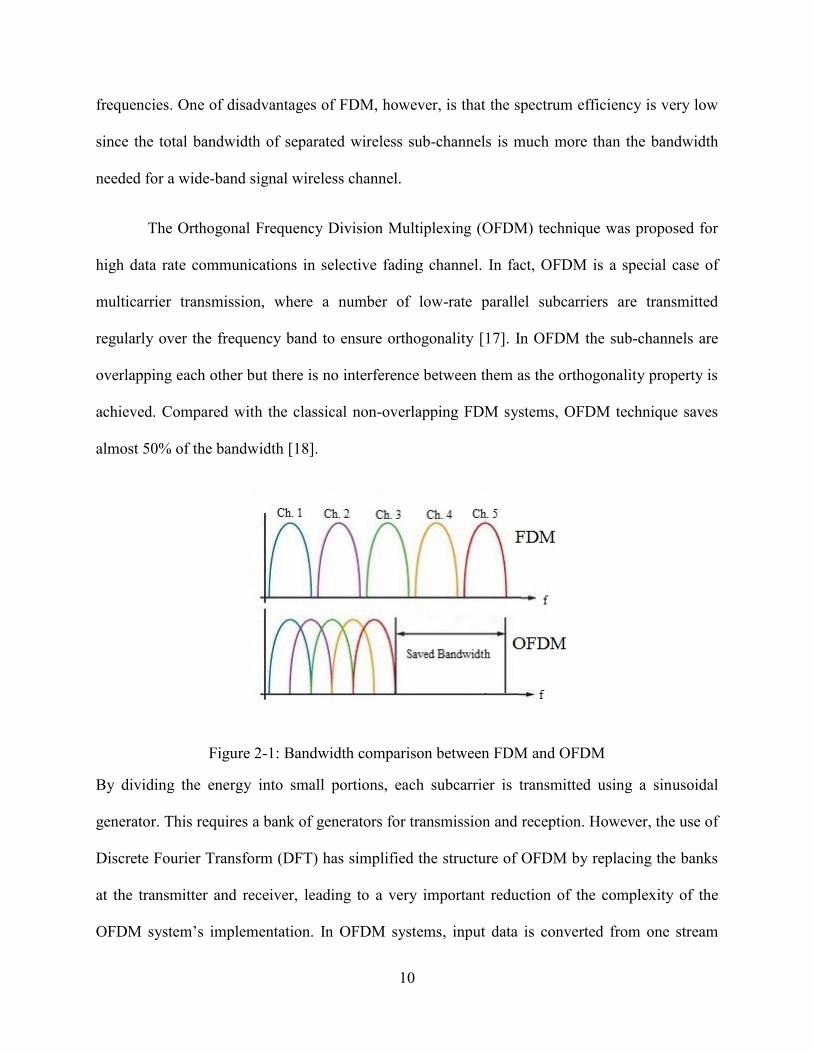
The Orthogonal Frequency Division Multiplexing (OFDM) technique was proposed for
high data rate communications in selective fading channel. In fact, OFDM is a special case of
multicarrier transmission, where a number of low-rate parallel subcarriers are transmitted
regularly over the frequency band to ensure orthogonality [17]. In OFDM the sub-channels are
overlapping each other but there is no interference between them as the orthogonality property is
achieved. Compared with the classical non-overlapping FDM systems, OFDM technique saves
almost 50% of the bandwidth [18].
Figure 2-1: Bandwidth comparison between FDM and OFDM
By dividing the energy into small portions, each subcarrier is transmitted using a sinusoidal
generator. This requires a bank of generators for transmission and reception. However, the use of
Discrete Fourier Transform (DFT) has simplified the structure of OFDM by replacing the banks
at the transmitter and receiver, leading to a very important reduction of the complexity of the
OFDM system’s implementation. In OFDM systems, input data is converted from one stream

11
data to parallel data stream by using serial to parallel converter (SPC), and then they are
modulated by Inverse Fast Fourier Transformer (IFFT). Thereby, the wide-band signal is broken
into narrow-band parallel signals when the rate of the input signal is divided by to become
the rate of each sub-signal. At the receiver, however, the data streams demodulated by Fast
Fourier Transformer (FFT) are converted to one data stream using parallel to serial converter.
In OFDM digital communication systems, the high-rate input data can be digitally
modulated by one or more digital modulate scheme such as BPSK, QPSK, 16-QAM and 64-
QAM. In this case the digital signal is mapped according to the modulation scheme and then is
broken into low-rate sub signals using serial to parallel converter to be fed to inverse fast Fourier
transformer. Multi-input signals can also be mapped separately with multiple modulation
schemes and fed to the same OFDM modulator but when they are converted from serial to
parallel, all the outputs of low-rate sub-signals have to have the same bit. In this thesis, QPSK
modulation has been discussed and used with OFDM modulation to create our QPSK-OFDM
system.
As OFDM has many advantages over single-carrier schemes, it has become very popular
for wideband digital communications and has been adopted for many communication systems
and standards such as Digital Video Broadcasting (DVB), Digital Audio Broadcasting (DAB),
Digital Subscriber Line (DSL), 4th
generation mobile communication and wireless networks
IEEE802.11a, g, n.
2.2 QPSK Baseband Modulation
Since linear digital modulation techniques are bandwidth-efficient, they are widely used
in wireless communication systems. PSK modulation techniques, such as BPSK, QPSK and

12
8PSK are linear modulations in which the phase of the transmitted signal varies according to the
input data. In QPSK modulation, every two bits are modulated to be one QPSK symbol and that
saves more bandwidth compared with BPSK modulation. The original signal stream with values
of 1 and 0 is mapped and divided into two streams in-phase and Quadrature streams as values
of , which have the half bit rate of the original data. The QPSK symbol can be only in one of
four states which are different in phase and equally spaced by π/2 such as 0, π/2, π or 3π/4. The
figure below depicts the constellation of QPSK symbol in two dimensions.
I
Q
(11) (00)
(01
) (1
0)
Sqrt(Es)
Figure 2-2: QPSK signal constellation
where is the symbol energy and is equal to twice (bit energy). As shown in Figure 2-2,
all QPSK symbols have the same energy but they have different phases. The probability of bit
error for coherent QPSK over additive white noise channel can be expressed [19] as
√
Bit Set I value Q value Phase
00 1 0 0
01 0 -1 270
11 -1 0 180
10 0 1 90
13
where ( )
√ ∫ (
)
and is noise spectral density.
2.3 Overview of OFDM System
OFDM was proposed as a Single-Input and Single-Output (SISO) technique to boost the
resilience over multipath frequency-selective fading. Each signal can be transmitted using one
orthogonal subcarrier or more when the signal has a high rate and needs to be divided into many
sub-channels. By applying the orthogonality theory for the transmitted subcarriers, OFDM
modulation provides high bandwidth efficiency. In this section basic analysis for OFDM is
discussed.
In the traditional multicarrier system, the transmitter consists of a set of modulators with
different carrier frequencies. Assuming complex symbols are to be transmitted by OFDM
modulation where , where is the number of subcarriers. The OFDM
signal can then be shown [20] as
( ) ∑
, for 0 ≤ t ≤
= + kΔ
whereas Δ is the subchannel frequency space and is symbol duration.
In OFDM the symbol duration must be =
to fulfill the orthogonality condition and avoid
any interference.
At the receiver side, the demodulated OFDM signal can be expressed as below
∫ ( )
=
∫ (∑
)

14
=
∫ (∑
) ( )
= (∑ )
∫ ( )
Since the subcarriers are orthogonal, we can derive the following equation:
∫ ( )
= (∑
) δ( )
where δ( )=
∫ ( )
= {
∫ ( )
=
As the processes of the modern communication systems are often represented digitally these
days, the OFDM signal can also be expressed digitally in a sampled-data style by substituting
n for t where is the sampling interval [21].
( ) ∑
Assume , where is the frequency spacing ( ) and OFDM is a digital baseband
modulation.
( ) ∑
Let =
and =
to satisfy the orthogonality condition.
( ) ∑
=

15
The input signal can be a real or complex symbol modulated by any digital
modulation scheme such as Binary Phase Shift Keying (BPSK), Quadrature Phase Shift Keying
(QPSK) or Quadrature Amplitude Modulation (QAM). The wideband input signal is divided
to parallel narrowband data stream by serious to parallel converter. In case of zero-padding
is broken into number of data streams where is less than or equal to , the size of
IFFT. The process of modulating these data streams to generate OFDM symbol is performed by
using IFFT, which makes the implementation of OFDM systems inexpensive and simple. In fact,
the FFT algorithm reduces the number of complex multiplications from to
for an N-
point DFT [2]. Since the spectrum of a square function is a function, the frequency
spectrum shape of the subcarriers is a shape unless OFDM symbol is shaped or windowed
to limit its bandwidth. As the amplitude of ( ) function is zero when is equal to
and is any integer number, any subcarrier has zero value wherever other subcarriers have the
maximum amplitude, and therefore the subcarriers do not interfere with each other. To get no
interference by satisfying the orthogonality property, the frequency space between the
subcarriers has to be equal to
. Otherwise, there will be intercarrier interference (ICI).
Figure 2-3: OFDM frequency spectrum

16
2.3.1 Guard Interval and Cyclic Prefix
Since OFDM symbol is made of multi narrow-band signals that have long symbol,
OFDM modulation is robust against multi-path delay spread when the delay is considered very
small compared with the symbol duration. To make OFDM completely resistant to the multipath
delay spread in radio channel, guard intervals can be inserted between long OFDM symbols with
a length enough to be larger than the maximum delay spread. At the receiver side, these guard
intervals which include the time-domain symbol interference will be removed, and the adjacent
symbols will be interference-free.
However if zero signal is sent during the guard time, intercarrier interference (ICI) will
occur and as a result the orthogonality property between the subcarriers can no longer be
preserved. To solve this problem, the OFDM symbol is extended cyclically in the guard interval
by replicating a part of OFDM symbol but it has to be an integer number of IFFT sampling time
and larger than the maximum expected delay spread. In this case the transmitted OFDM signal
will still be periodic as it is very significant to maintain the orthogonality.
The cyclic extension can be done by three different ways; cyclic prefix, suffix or timing
advance. The common way is cyclic prefix since it is simple to implement and does not need to
rotation processes at the receiver side as in the cyclic suffix. Adding guard intervals between
OFDM symbols, however, reduces the spectral efficiency.

17
Figure 2-4: OFDM cyclic prefix
2.3.2 Pulse Shaping
As OFDM signal consists of N number of unfiltered sinc-shaped subcarriers, the
frequency spectrum of OFDM can be band-limited depending on the number of subcarriers.
While the sinc-shaped subcarriers are orthogonal and overlapping each other, the spectrum of
OFDM side-lobes decreases rapidly where it is close to the band. Therefore, the larger number of
subcarriers is the more rapidly the spectrum decreases. Figure 2-5 shows the power spectrum
density of QAM- OFDM signal with different number of subcarriers.

18
Figure 2-5: OFDM Power spectrum density for different N subcarriers
Moreover the length of the extended interval has an effect on the spectrum of an OFDM
signal. The out of band spectrum also decreases more rapidly when the OFDM symbol is
extended with a cyclic prefix [2]. If OFDM bandwidth has to be band-limited with specified
boundaries, spectrum masks have to be applied for each channel before IFFT. This technique is
called windowing, when the signals pass through rectangular filters to eliminate undesired
sidelobes and limit the transmission spectrum. As a result, the spectrum of windowed OFDM
symbol goes down to zero more rapidly at the boundaries depending on window type and
specifications. The raised cosine window is commonly used and popular in wireless
communications. Its form is defined as

19
W(t) =
{
(
( )
) ( )
( )
( ( )
) ( )
where and are the number of samples for guard interval and OFDM symbol respectively.
The parameter β is the roll-off factor. Besides windowing, a conventional low-pass filter can be
applied to the baseband OFDM signal to suppress the out of band sidelobes. Compared to low-
pass digital filtering, the windowing technique is less complex to implement since fewer
multiplications are needed in time domain rather than convolution in case of filtering technique.
2.3.3 Peak to Average Power Ratio
Since OFDM signal is a summation of multiple sinusoidal signals, occasionally high
amplitudes of the sinusoidal signals can be added concurrently when they form an OFDM signal.
Consequently the amplitude of ODFM signal gets a very high level compared to the average
amplitude level. As a result, the complexities of both Digital to Analog Convertors (DACs) and
Analog to Digital Converters (ADCs) increase to deal with the high level of signal, and radio
frequency efficiency decreases. As a matter of fact, when this OFDM signal with high amplitude
passes a power amplifier in the transmitter side, nonlinear amplification occurs as the power
amplifier. This OFDM problem of large peak is known as Peak to Average Power Ratio (PAPR)
considered as a disadvantage of using OFDM modulation. PAPR can be defined by the formula
shown below [21].
( )
( )

20
Many approaches have been proposed to reduce the PAPR, such as coding, signal distortion and
scrambling techniques.
2.4 Wireless Fading Channel
Using wireless communications technology has given many advantages over wire
communication systems in term of mobility, simplicity of accessing and installation but it is still
limited in some characteristics such as spectrum, capacity and reliability. There are many
unpredictable factors that can affect a signal transmitted into a wireless radio channel. The
channel variations and the user movement make the wireless radio channel time-varying and
dynamic. The wireless radio fading channel can be classified under different categories such as
small or large fading, flat or frequency selective fading and slow or fast fading. In this section
the multipath fading channels will be discussed to show the advantages of using OFDM
modulation.
2.4.1 Small-Scale Fading Channel
In mobile radio channel, a signal is transmitted as an electromagnetic wave with radio
frequency (RF) and is affected by different physical phenomena: reflection, diffraction and
scattering. Therefore, the transmission signal takes two or more different paths to get to the
receiver due to the wireless channel environment. When different versions of the transmission
signals arrive at the receiver antenna, the received signal will be a combination of signals that
have different delays and attenuations.

21
LOS
NLOS
NLO
S
NLOS
NLO
S
Figure 2-6: Multipath fading
The figure above is an example of multipath fading when the cell phone of the driver
receives many versions of the transmission signal including the line-of-sight (LOS) propagation.
Also there is some non line-of-sight (NLOS) propagation when the signal does not travel to the
receiver in a straight line as it may be reflected, diffracted or refracted in the radio channel
environment.
In multipath fading, the received signal is rapidly fluctuating in amplitude, phase and
frequency [21]. The fading phenomenon can have two versions which are small-scale and large-
scale fading [22]. In large-scale fading, the channel has a large scale of attenuation that occurs as
path loss and shadowing, as it is the case with mobile station user moving in a large distance.
The small-scale fading, on the other hand, occurs when different versions of the transmission
signal arrives at the receiver with a slight difference in time. In other words, the channel rapid

22
variation will be in a small region when the movement of the mobile station is in a small
distance.
Due to the destructive and constructive interference of multipath, the received signal
rapidly varies in strength, delay and frequency. Receiving many versions of the transmission
signal at different times causes a variation of the amplitude and phase of the received signal,
which is a combination of the multipath waves. The random change in frequency is caused by
the variation of Doppler shifts on different multipath signals. Small-scale fading is influenced by
many physical factors such as the speed of mobile station, transmission bandwidth of the signal,
multipath propagation and speed of surrounding objects [19]. The most significant small-scale
fading effects in radio channel can be characterized by two sorts of dispersions that are
frequency dispersion and time dispersion [21].
2.4.2 Frequency Dispersion
In wireless communication systems if one of the receivers, transmitters or the scatters
moves around during the communication, Doppler spread will occur in the received signal due to
the frequency dispersion. In other words, the receiver signal will have shifted spectrum and that
frequency shift depends on the speed of the moving stations and the angle between the directions
of the movement and signal reception. Figure 2-7 illustrates the frequency dispersion between
two stations.
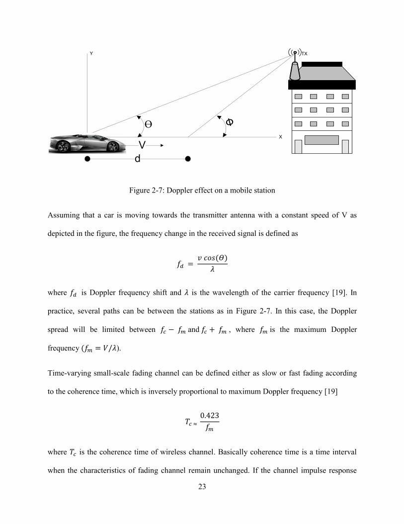
23
TX
X
ϴ Ф
Y
V
d
Figure 2-7: Doppler effect on a mobile station
Assuming that a car is moving towards the transmitter antenna with a constant speed of V as
depicted in the figure, the frequency change in the received signal is defined as
( )
where is Doppler frequency shift and is the wavelength of the carrier frequency [19]. In
practice, several paths can be between the stations as in Figure 2-7. In this case, the Doppler
spread will be limited between and , where is the maximum Doppler
frequency ( ).
Time-varying small-scale fading channel can be defined either as slow or fast fading according
to the coherence time, which is inversely proportional to maximum Doppler frequency [19]
where is the coherence time of wireless channel. Basically coherence time is a time interval
when the characteristics of fading channel remain unchanged. If the channel impulse response

24
does not change significantly during the one or more symbol period , the small-scale
fading is considered slow.
2.4.3 Time Dispersion
When a signal is sent wirelessly, many version of that signal with different power arrive
at the receiver at different times due to distinctive paths they take. The delay spread resulting
from distinctive paths causes interference between symbols, which is known as intersymbol
interference. The coherence bandwidth can be calculated by measuring the delay spread of
wireless channel. In fact the root mean square of delay spread is inversely proportional to
coherence bandwidth [21].
According to the relationship between the coherence bandwidth and the delay spread, a
wireless channel with large delay spread has a narrow coherence bandwidth. As a result a signal
that has a wide bandwidth wider than the coherence bandwidth will endure frequency
selective fading causing inter symbol interference, whereas a signal with bandwidth much
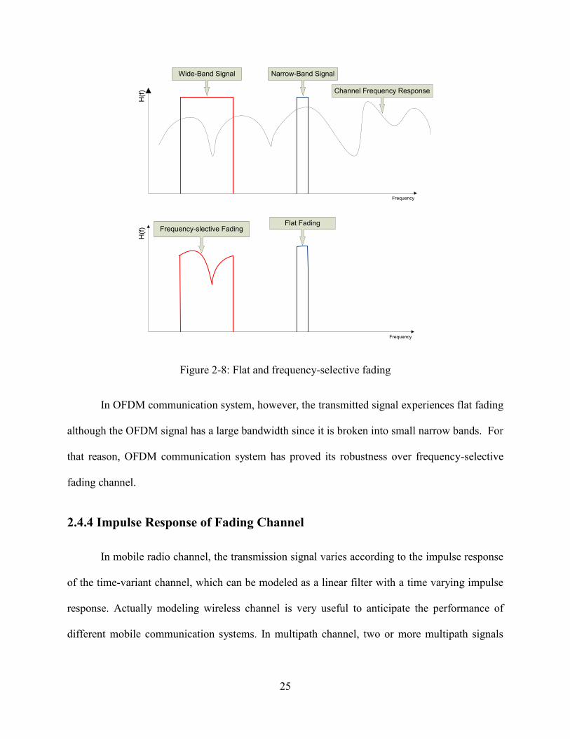
smaller than the coherence bandwidth will endure flat fading. In other words, the ratio
between coherence bandwidth and signal bandwidth can imply if the signal tolerates flat or
frequency-selective fading. Therefore radio channel can be under one of two categories: flat or
frequency-selective fading. Figure 2-8 illustrates how dissimilar-band signals can endure
different types of fading.
25
Flat FadingFrequency-slective Fading
Narrow-Band Signal Wide-Band Signal
H(f
)H
(f)
Frequency
Frequency
Channel Frequency Response
Figure 2-8: Flat and frequency-selective fading
In OFDM communication system, however, the transmitted signal experiences flat fading
although the OFDM signal has a large bandwidth since it is broken into small narrow bands. For
that reason, OFDM communication system has proved its robustness over frequency-selective
fading channel.
2.4.4 Impulse Response of Fading Channel
In mobile radio channel, the transmission signal varies according to the impulse response
of the time-variant channel, which can be modeled as a linear filter with a time varying impulse
response. Actually modeling wireless channel is very useful to anticipate the performance of
different mobile communication systems. In multipath channel, two or more multipath signals

26
arrive with different amplitude, frequency and time. The channel impulse response can be
expressed as
( ) ∑ ( ) ( ( ))
( )
where Ʈ is the time delay; is the phase shift; is the unit impulse function; is the path
gain; is the path index; and N is the number of multi paths [19] [23]. Since the multipath
channel works like a band-limited band-pass filter, the received signal will be equal to the
transmission signal convolved with the impulse response of the channel as depicted in the
equation below [24].
( ) ∫ ( ) ( ) ( ) ( )
In the small-scale fading, the channel impulse response can be time-invariant over certain
time or area, and that simplifies the radio channel modeling. In digital wireless communications,
the channel can be modeled as a linear finite impulse response filter. This type of modeling will
be discussed in Chapter 3 when the channel is needed to be modeled to verify the performance
for wireless communication systems.
2.5 LTE Physical Layer Downlink Parameters
Since our OFDM is based on the LTE downlink physical layer, some basic parameters
have to be specified according to the 3GPP specifications. The initial LTE requirements were
defined by 3GPP in a way that LTE physical layer should support data rate of 100Mbps and

27
50Mbps for downlink and uplink, respectively. To fulfill these requirements, OFDM is employed
as a modern technique for mobile communications. Due to the channel variation in time and
frequency domains, the LTE interface supports Frequency Domain Duplexing (FDD) and Time
Domain Duplexing (TDD). The LTE transmission is segmented into frames. Based on radio
frame structure type1, each frame has a time duration of 10 ms, and it consists of 10 sub-frames
[25] [26]. As depicted in Figure 2-9, a sub-frame consists of two slots with time duration of 0.5
ms.
0 1 2 3 4 5 6 7 8 9
Slot # 0 Slot # 1
0 1 2 3 4 5 6
CP OFDM Symbol
Subframe
Frame (10ms)
OFDM
T=0.5ms
Figure 2-9: Radio frame structure type 1
One slot is composed of seven or six OFDM symbols depending whether an extended or normal
CP is used. These symbols have subcarriers ranging from 128 to 2048 determined by the
transmission bandwidth.

28
.As LTE supports a scalable transmission bandwidth, the number of subcarrier can be
different according to the transmission bandwidth assuming the same subcarrier spacing of 15
kHz. In fact the LTE PHY specification is designed to have multiple transmission bandwidths
from 1.4 MHz to 20 MHz [27]. Each bandwidth specifies the number of occupied subcarriers,
which is related to FFT size. Different FFT sizes of 128 to 2048 are supported depending on the
transmission bandwidths as demonstrated in Table 2-1 [28]. Two types of CP, normal and
extended CPs are allowed in LTE specifications depending on the extensive delay spread of the
environment.
Transmission BW 1.4 MHz 3 MHz 5 MHz 10 MHz 15 MHz 20 MHz
DFT Size 128 256 512 1024 1536 2048
No of CP
samples
Normal 9 18 36 72 108 144
Extended 32 64 128 256 384 512
Table 2-1: Typical parameters for downlink transmission
In case of 5 MHz bandwidth, the FFT size and sampling frequency could be 512 and 7.68MHz
respectively for efficient implementation. The normal and extended CPs have lengths of 36 and
128 samples respectively. Based on the 5MHz-bandwith LTE specifications, our OFDM is
modeled and implemented in the following chapters.
2.6 Summary
In this chapter, introduction of OFDM modulation was presented with its advantages
compared with traditional FDM modulations. The concept of QPSK modulation was presented

29
with some background information. In fact, OFDM modulation and demodulation was explained
theoretically with the equations of signal processes for IFFT and FFT. Cyclic prefix and pulse
shaping were illustrated. Peak to Average Power Ratio (PAPR) was illuminated as a
disadvantage of OFDM modulation. Wireless channel was analyzed in details including small-
scale fading, impulse response, time dispersion and frequency dispersion. Finally the 3GGP LTE
downlink PHY layer parameters were provided specifying our OFDM system parameters as the
basis for further modeling and implementation. In the following chapters, the OFDM system
based on the LTE parameters is modeled, simulated and implemented according to design flow
methodology.

30
Chapter 3
OFDM System Design and Simulation
In order to design and implement an OFDM system, four stages are taken according to
design flow illustrated in Figure 3-1. In each stage, the OFDM system is modeled and simulated
to obtain simulation results that achieve high performance before going onto the next stage. In
this chapter, the design flow of an OFDM system is proposed. The first two stages of the design
flow, which are MATLAB and Simulink modeling and simulation, are discussed in this chapter.
3.1 Design Flow
As shown in Figure 3-1, the design flow of OFDM system is composed of four stages.
The first stage is to model and simulate in MATLAB two OFDM systems that have different
cyclic prefixes. Based on the mathematical basis of OFDM system expressed in Chapter two,
two OFDM systems are modeled and simulated in MATLAB based on parameters for 3GPP
LTE. Using floating-point representation, these two systems are verified under different wireless
fading channels to show the difference between these OFDM systems.

31
Floating-point modeling and simulation in MATLAB
Floating-point modeling and simulation in Simulink
Fixed-point hardware modeling and simulation
using Simulink & Xilinx System Generator
Hardware verification on Virtex-5 FPGA Platform
through hardware co-simulation
Figure 3-1: Implementation design flow
To evaluate the performance of communication systems, the bit error rate versus bit
energy to noise spectral density ( / ) is found using Monte Carlo simulation. By comparing
the BER curve of simulation results for QPSK-OFDM systems with the theoretical QPSK BER
curve, the performance of each OFDM system is evaluated and analyzed.
In the second stage, the OFDM system with extended cyclic prefix is modeled based on
LTE downlink parameters and simulated in the Simulink environment. Unlike MATLAB, many
parameters in Simulink environment such as the sampling period have to be determined. As
OFDM model has different sampling rates, OFDM model-based design is divided into multi-rate

32
subsystems. In fact, Simulink is a graphical extension to MATLAB for the modeling and
simulation of multi-rate system with different simulation time steps. Using the Simulink
communication library, the OFDM system is modeled based on the model in MATLAB. Each
Simulink block represents a mathematical formulation that has already been implemented in
MATLAB. The model-based design is simulated using floating-point representation. In order to
draw the BER curve of the OFDM design, the input and output data of the Simulink is stored in
MATLAB workspace for analyzing and visualization. This Simulink OFDM model is considered
the basis for Xilinx based implementation by replacing the Simulink blocks with Xilinx blocks.
However, some Simulink blocks such as data source and sinks are still required for hardware co-
simulation.
Designing an OFDM system using Xilinx blocks is the third stage of the design flow. In
this stage the float-point Simulink blocks are replaced by fixed-point Xilinx blocks if possible.
Some Xilinx subsystems are designed to have the same functionality of the Simulink blocks.
Using fixed-point representation leads to a compromise between the system performance and the
size of Xilinx OFDM design since the number of assigned bits in fixed-point representation
affects the system performance. The larger number of assigned bits, the more complex hardware
design. The number of assigned bits is chosen to make the size of hardware design suitable for
Xilinx Virtex-5 FPGA implementation with high performance.
The final stage of the design flow is to verify the Xilinx-based design in actual hardware.
First, the design is compiled to a hardware co-simulation block using Xilinx system generator
that coverts Xilinx designs into bit streams ready to be downloaded on an FPGA. The hardware
co-simulation block is then tested in Simulink environment although the design is actually
running on Xilinx Virtex-5 FPGA. In other words, the hardware design is incorporated in
33
Simulink design. As result, the Xilinx OFDM design is tested and verified on Xilinx Virtex-5
FPGA through hardware co-simulation. Evaluating the system performance is done by
comparing the BER of hardware co-simulation and theoretical QPSK modulation under
frequency-selective fading.
3.2 Floating-Point Modeling and Simulation in MATLAB
In order to perform tasks in digital communications and digital signal processing,
MATLAB software has been efficiently used for simulation, testing and evaluation of the system
performance. OFDM system design has to be tested before it can be implemented to avoid any
design error. Therefore, our OFDM system is modeled and simulated in MATLAB and
Simulink, before the VHDL code is generated and downloaded to ML506 Virtex-5 board for
implementation. For better understanding of signal modulation processes, each stage in OFDM
modulation is described and elaborated in this chapter. Since the receiver performs the inverse
processes of the transmitter, only the transmitter blocks are detailed.
The LTE downlink transmission scheme is based on OFDM modulation. To model an
OFDM system based on 3GPP LTE parameters, the OFDM specifications have to be defined
according to the transmission bandwidth. Using the LTE 5MHz-bandwidth downlink parameters,
two OFDM systems with normal and extended CP are modeled in MATLAB with fixed-point
representation. As explicated in Table 2-1, the IFFT size of 5 MHz transmission bandwidth is
512 which represent the number of OFDM subcarriers. The normal and extended CP samples are
36 and 128 samples respectively.

34
Random
Data
Generation
QPSK
modulation
Reshaping
data
(S/P)
Zero
paddingIFFT
Adding
Cyclic
Prefix
Generating
Channel
impulse
response
Convolution
+Generating
AWGN
Reshaping
data
(S/P)
Reshaping
data
(P/S)
Removing
Cyclic
Prefix
FFTZero
Puncturing
Reshaping
data
(P/S)
QPSK
Demodulati
on
One-tap
Equalizer
with perfect
channel
knowledge
Error rate
calculation
TX
RX RX
Figure 3-2: Block diagram of an OFDM transceiver
3.2.1 Random Data Generation
In the first stage an m-by-n digital random data matrix is generated with the condition
that it has to have only scalar values of either 0 or 1 with the same probability in order to be
similar to the original digital signal in digital communication. To determine the size of the
matrix, many factors have to be considered such as number of OFDM symbols, FFT size,
number of zeros padded and modulation technique. A large size of input matrix can cause the
computer to run out of memory, depending on the RAM of the computer. In our design, FFT has
a size of 512, the number of OFDM symbols is and QPSK modulation is used. Assuming
256 zeros are padded in one OFDM symbol, the number of bits per OFDM symbol is represented

35
as (512-256)*k = 512, where k =2 is the modulation index for QPSK. As a result, the size of the
random matrix is defined as
( )
For simplicity, number of columns is assumed to be 1, so , number of rows is 6* .
Actually, this determination of the random matrix size is to ensure that the number of QPSK
symbols after zero padding can be reshaped to be a multiple number of FFT size with no
remains. However, the number of OFDM symbol per matrix can be as small integer value as one,
but many matrices have to be generated to reach the number of OFDM symbols required to draw
BER curve. Assuming the original message where n is from 1 to M, the original data matrix is
represented as
3.2.2 QPSK Modulation
The data to be sent on each carrier is mapped into a QPSK format before it is modulated
by OFDM. Every two serial bits of the original digital data are mapped onto a corresponding
QPSK symbol that is different in phase angles 0, 90, 180 or 270. Each two bit group is encoded
to In-phase or Quadrature axis. Therefore, each QPSK symbol can be represented as a complex
number if the constellation in Figure 2-2 is used for
mapping. The constellation with zero phase-offset is used in our implementation. According to
phase shift keying modulation, the amplitude of PSK symbols is constant, so QPSK symbols
have the same energy, although they have different phases.

36
The original data matrix is modulated into a matrix of complex numbers as QPSK symbols and
the size is equal to the half size of the original matrix. The modulated data matrix is depicted as
where is a QPSK symbol represented in a complex number.
3.2.3 Serial to Parallel Conversion
In this section the serial data is converted to parallel data. The modulated matrix S, as the
input matrix, is reshaped to be a matrix that has 256 columns. In this case, each row of 256
QPSK symbols is considered to be parallel data. These 256 QPSK symbols are grouped to be
modulated to create an OFDM symbol. Actually the purpose of reshaping is to form the S matrix
to be ready for OFDM modulation using IFFT. The new form of modulated matrix can be
expressed as
{
( )
( )
( )
( )
}

37
3.2.4 Zero Padding
For better performance, the frequency spacing between the subcarriers in OFDM frequency
domain can be decreased when the sampling rate increases. To increase the sampling rate,
oversampling is used by appending zeros to the end of the original data sequence. As zeros are
padded in a signal, the number of samples in time domain increases which also increases the size
of FFT. As a result of extending FFT samples, OFDM symbol will have a higher resolution
needed for digital signal processing such as digital to analog and analog to digital conversions.
Oversampling process has to follow the Nyquist sampling theorem to avoid aliasing problem that
may happen in frequency domain. Therefore the Nyquist rate has to be at least twice the highest
frequency in the sampled signal [29]. As the number of samples for FFT is 256, the number of
zeros appended has to be at least 256 to meet the Nyquist theorem. To ensure that non-zero data
are mapped onto subcarriers close to zero frequency and zero data are mapped onto the high
positive/negative-frequency subcarriers, these zeros should be padded in the middle of each
parallel IFFT data input.
The oversampled matrix D can be illustrated as
{
( )
( )
( )
( )
( )
( )
}

38
3.2.5 Inverse Discrete Fourier Transformer
To generate multiple orthogonal subcarrier signals overlapped in spectrum, Discrete
Fourier Transformer (DFT) and Inverse Discrete Fourier Transformer (IDFT) processes should
be used. In MATLAB, FFT and IFFT have been used to implement DFT and IDFT processes. In
fact, the FFT function in MATLAB uses several algorithms in combination including Cooley-
Tukey [30], splid-radix [31] and prime factor algorithms [32]. To use decimation-in-time, the
number of IFFT points N has to be an integer of power 2, and that is why the modulated matrix
is reshaped to have 256 columns and then zero padded to have 512 columns which meets the
requirement of decimation-in-time algorithms. As result the transpose of IFFT output matrix is
represented as matrix X shown below.
{
(
)
(
)
(
)
(
)
}
Each row of X matrix is representing OFDM symbol, which is periodic with a period of 512
samples.
3.2.6 Adding Cyclic Prefix
In this stage OFDM symbol is cyclically extended to eliminate ISI between consecutive
symbols. The process of prefixing an OFDM symbol by repeating the end of OFDM is known as
cyclic prefix. In order to make the OFDM system robust to multipath fading, the cyclic prefix
should be larger than the maximum delay spread. Using the OFDM modulation parameters for
3rd
Generation Partnership Project Long term Evolution (3GPP LTE), two cyclic prefix lengths

39
are used to compare the system performance over different multipath fading channels [28]. The
normal CP added to OFDM symbol is 36 samples, while the extended CP is 128 samples. In fact
an extended CP is more suitable, when the environment has very extensive delay spread. As two
different CPs are deployed, two OFDM symbol matrices represent
different OFDM modulation designs as depicted
{
}
{
}
3.3 Channel Modeling
Many types of wireless channels can be modeled using MATLAB depending on the
channel specifications. To show the main advantage of OFDM modulation, small-scale fading
channel should be modeled and implemented in our OFDM design. As explained in the previous
chapter, fading channel can be specified according to the channel characteristics and the
transmission scheme. Doppler spread and multipath delay spread are the main parameters used to

40
define wireless channel. Also depending on the signal parameters, the wireless channel can vary
for signals that have different parameters such as bandwidth and symbol period [22]. For
instance, the same wireless channel can be frequency-selective fading for a signal that has a wide
bandwidth, and it can be frequency-non-selective fading for a signal that has a narrow
bandwidth. To facilitate generating fading channel, wireless environments can be either LOS or
NLOS, which are considered to follow Racian and Rayleigh distributions respectively. In NLOS
environment, the fading can be represented as a complex Gaussian random variable +j
where and are identically-distributed independent Gaussian random variables with a zero
mean and variance of . Assuming Z Rayleigh random variable is the amplitude of the complex
random variables, the probability density function of Z is represented as
( )
Where √
and is the variance of and .
To generate the Rayleigh random variable Z using MATLAB, two Gaussian random
variables with zero mean and unit variance, and are generated using built-in MATLAB
function.
√
The average power of the Rayleigh random variable is . As the transmitted signal
has zero-dB power, the fading variable has to have the same average power of the transmitted
signal. Therefore, the Rayleigh random variable generated by MATLAB is divided by √ .

41
In LOS environment, a constant is added to complex Gaussian random variables to represent a
strong direct path between the transmitter and the receiver +j .
The QPSK-OFDM design has single input and single output, and the channel model is
also Single- Input Single-Output (SISO). Assuming low mobility in a small coverage area, the
fading channel used in the design is modeled to be an indoor channel that can be static or quasi-
static. The characteristics of static channel do not change during the data transmission at given
time and location, while the characteristics of quasi-static channel change during the symbol
duration.
To implement multipath fading channel, some aspects are important to define the channel
model such as number of paths, type of propagation, maximum Doppler shift, time delay and
path gain. As an indoor channel is used in the QPSK-OFDM design, the two popular indoor, 2-
ray model and exponential model are discussed below.
One approach to model the wireless channel is Two-ray model. In this model, two rays
with the same power are used to represent the channel paths; one path with zero delay and other
path with the maximum excess delay . The maximum excess delay is twice the mean excess
delay ̅. Since there are only two paths and one of them has zero delay, the mean excess delay is
equal to the root mean square (RMS) delay . As the first path has always constant power
and zero delay, the parameters of the second path determine the channel characteristics. In
practice the second path has less power than the first path but in 2-ray model both paths have the
same power for simplicity. Therefore, when accuracy is needed, 2-ray model might not be a good
choice for channel modeling [22].

42
Another method for modeling the wireless channel is exponential model. In the
exponential model, there are more than two paths that have different powers decreasing
exponentially with the channel delay. This type of model is highly likely used to represent an
indoor channel since the average channel power decreases rapidly as the delay increases. The
power delay profile (PDP) for the exponential model is expressed as
( )
As a discrete-time model is required in MATLAB, the PDP of exponential model that depends
on the delay can be represented with sampling time as
( ) ( ) ,
where is the discrete time index, is the last path index and ( )
( ) is the first path power.
Figure 3-3: Exponential and 2-ray models

43
As the exponential model is more accurate than 2-ray model, the wireless fading channel
is modeled using the exponential model. Many wireless fading channels that have different
delays are modeled to evaluate the robustness of the two OFDM systems, extended-CP and
normal-CP OFDMs, against frequency-selective fading. While the delay spread determines the
PDP, the maximum excess delay and the sampling time define the number of paths for each
channel. In other words, the channel characteristics for exponential model depend on sampling
period, RMS and maximum excess delays.
To implement Wireless channel using MATLAB, time-variant channel impulse response
(t) is generated according to the delay spread and sampling period. However, we assume that
the fading is slow, so channel remains invariant with no change during the period of OFDM
symbol. That means that the coherent time of the wireless channel is smaller than the symbol
period.
Firstly a 1-by- matrix of complex Gaussian random values with zero mean, unit
variance and normalized power is generated to create Rayleigh random values ( ). Those
values are then multiplied by the PDF values, ( ) ( ) ( ) to create the impulse
response ( ) of the particular channel. However this procedure is repeated for each OFDM
symbol to ensure channel variation in the time domain.
[ ]
[
] [ ]
When a channel model has taps, it does not mean that the channel has paths. What it means
is that channel impulse response has non-negligible values at the sampling time (

44
). There may be two or more propagation paths with different delays in a wireless
channel that can be modeled as an -tap discrete-time model.
Secondly each OFDM symbol is convolved with each channel impulse response
generated as if the wireless channel works as a filter for the transmission signal, except that the
channel impulse response varies for every OFDM symbol. Since there are two OFDM systems,
extended-CP and normal-CP, the same channel is applied on both OFDM systems.
The final part of modeling is adding Additive White Gaussian Noise (AWGN) to the
convolved signal. To do so, two matrices of AWGN with the same size of matrices
and respectively are generated in MATLAB to be added to the two matrices
of convolved OFDM symbols as following
Since the transmission signal is complex, the AWGN is complex with power level that depends
on the signal to noise ratio for OFDM symbol SNR. However, SNR can be determined from the
ration of QPSK symbol energy to noise power spectral density
⁄ ( ) ⁄ ( ) ( )
where ⁄ is the bit energy to noise power spectral density and is the number of
information bits per symbol. If is the OFDM symbol period and is the
sampling period,
=

45
However, zero-padding has an effect on OFDM symbol power since the OFDM symbol
will be consisting of QPSK symbols and zeros. Therefore, the OFDM symbol power will be less
if there is no zero-padding. In other words, zero-padding has to be under consideration to define
the AWGN channel noise level to specify the variance added per symbol.
Adding cyclic prefix to the OFDM symbol does not have an effect on the AWGN
channel level since the OFDM symbol extension is a part of OFDM symbol. On the other hand,
the number of information bits per symbol is influenced by the code rate if channel coding is
used in the communication system.
3.4 MATLAB Simulation Results
In order to verify the designed system, the performance of design has to be as close as
possible to the theoretical performance. In communication systems, bit error rate is used to show
the performance of the systems. Therefore, we use MATLAB to implement the design, simulate
and analyze the results.
The QPSK-OFDM design is tested under both Rayleigh fading, flat and frequency-selective
fading, and results are analyses and simulated.
Experiment 1: The Effect of Flat Fading Channel
In flat fading the discrete channel response ( ) has only one tap that will be
convolved with the OFDM symbol.

46
Figure 3-4: BER of the OFDM systems under flat fading channel
This means the wireless channel has one discrete path with complex path gain and
normalized power. To create this Rayleigh fading channel conveniently, two uncorrelated zero-
mean Gaussian random variables are generated to be the real and imaginary parts of the channel
response.
As shown both extended and normal CP QPSK-OFDM systems have the same
performance when they tolerate flat fading channel. Actually their BERs match the theoretical
QPSK BER assuming the perfect channel estimation. As a result, the length of the OFDM guard
interval does not have any effect on the performance when the fading is flat since there is no
Intersymbol interference.
0 5 10 15 20 25 3010
-4
10-3
10-2
10-1
100
Eb/No (dB)
BE
R
Bit error probability curve for QPSK-OFDM
Extended-CP QPSK-OFDM
Normal-CP QPSK-OFDM
Theoretical QPSK over falt fading
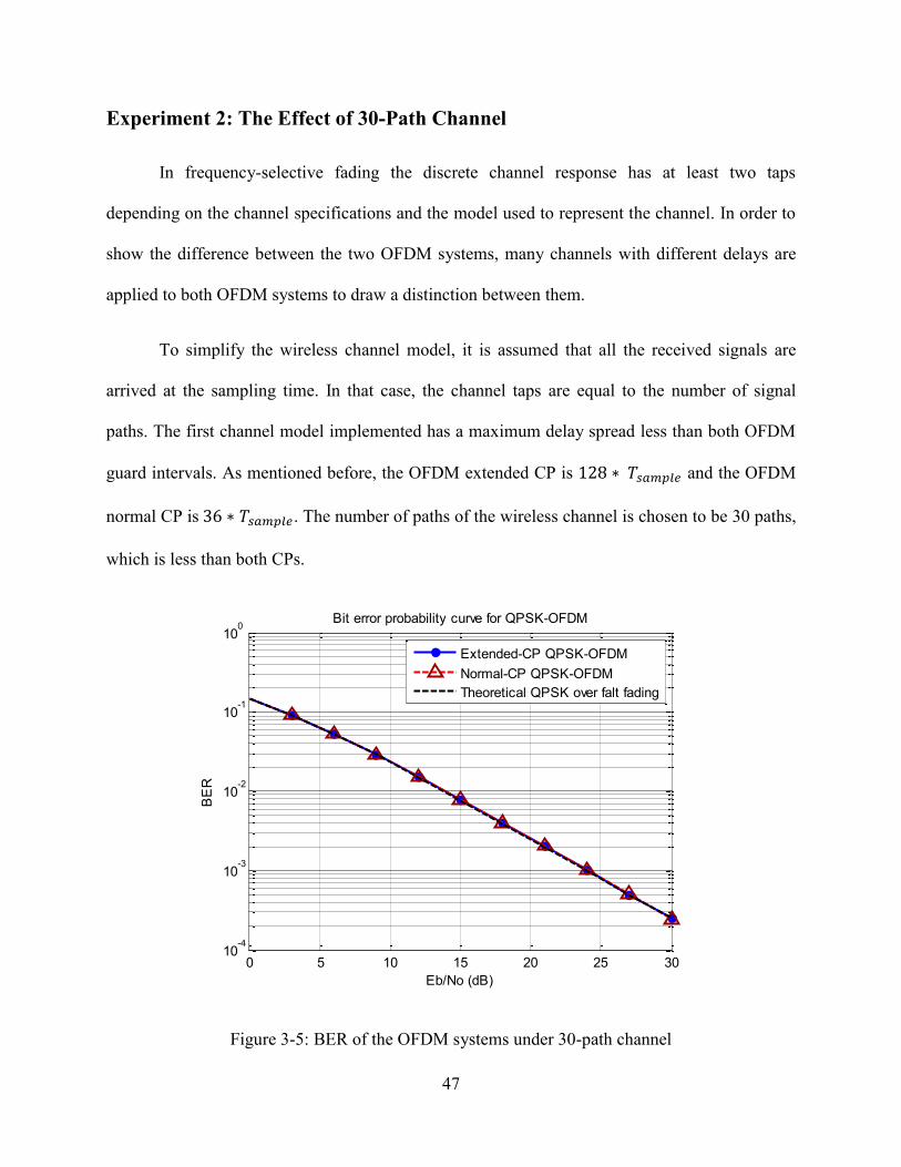
47
Experiment 2: The Effect of 30-Path Channel
In frequency-selective fading the discrete channel response has at least two taps
depending on the channel specifications and the model used to represent the channel. In order to
show the difference between the two OFDM systems, many channels with different delays are
applied to both OFDM systems to draw a distinction between them.
To simplify the wireless channel model, it is assumed that all the received signals are
arrived at the sampling time. In that case, the channel taps are equal to the number of signal
paths. The first channel model implemented has a maximum delay spread less than both OFDM
guard intervals. As mentioned before, the OFDM extended CP is and the OFDM
normal CP is . The number of paths of the wireless channel is chosen to be 30 paths,
which is less than both CPs.
Figure 3-5: BER of the OFDM systems under 30-path channel
0 5 10 15 20 25 3010
-4
10-3
10-2
10-1
100
Eb/No (dB)
BE
R
Bit error probability curve for QPSK-OFDM
Extended-CP QPSK-OFDM
Normal-CP QPSK-OFDM
Theoretical QPSK over falt fading

48
As demonstrated in Figure 3-5, the BER of extended CP and normal CP QPSK-OFDM
matches the theoretical QPSK BER for flat fading. This result indicates that OFDM symbols do
not encounter any ISI, even though channel is a multipath channel. The BER of OFDM
manifests the robustness of OFDM against frequency-selective channel.
Experiment 3: The Effect of 100-Path Channel
In the third channel model, the channel is chosen to have 100 paths with maximum delay
spread of 100* on the assumption that all OFDM symbol signals arrived at the sampling
time.
Figure 3-6: BER of the OFDM systems under 100-path channel
0 5 10 15 20 25 30 35 4010
-5
10-4
10-3
10-2
10-1
100
Eb/No (dB)
BE
R
Bit error probability curve for QPSK-OFDM
Extended-CP OFDM, CP=128, No.Paths=100
Normal-CP OFDM, CP=36, No.Paths=100
Theoretical QPSK over Flat Fading

49
As the normal-CP QPSK_OFDM symbol has a guard interval of that is less
than the maximum delay spread, the OFDM symbol experiences ISI and Frequency-selective
fading demonstrated in the BER of normal-CP OFDM. On the other hand, OFDM symbol with
extended-CP does not encounter any ISI since its guard interval is more than the
maximum delay spread of the channel model. Therefore, the extended-CP QPSK-OFDM signal
encounters channel flat fading as depicted in Figure 3-6.
Experiment 4: The Effect of 140-Path Channel
In this experiment, the channel model has a maximum delay of 140* that exceeds
both OFDM symbol extensions. Therefore the OFDM symbols certainly encounter ISI.
Figure 3-7: BER of the OFDM systems under 140-path channel
0 5 10 15 20 25 30 35 4010
-5
10-4
10-3
10-2
10-1
100
Eb/No (db)
BE
R
Bit error probability curve for QPSK-OFDM
Extended-CP OFDM, CP=128, No.Paths=140
Normal-CP OFDM, CP=36, No.Paths=140
Theoretical QPSK over Flat Fading

50
Although extended-CP and normal-CP OFDM symbols are going through frequency-
selective fading, extended-CP OFDM system has better performance than normal-CP OFDM
system’s performance as shown in Figure 3-7. Due to the difference in the length of guard
intervals, the effect of ISI on OFDM symbols is unequal. In fact, longer guard interval results in
a better performance OFDM system.
3.5 Floating-Point Modeling and Simulation in Simulink
Since the communication toolbox in MATLAB Simulink implements a variety of tasks
for communication system design and simulation, our OFDM system is implemented in
Simulink using floating-point representation. Due to the communication toolbox capabilities of
computations, the communication system toolbox has algorithms for designing the physical layer
of communication systems including source coding, channel coding, interleaving, modulation,
channel models, equalization and synchronization [33]. It also has the visualization and graphical
tools to analyze the performance of communication systems. Using DSP blockset toolbox in
Simulink, designers can implement DSP functions used in MATLAB code. Not only can a
model-based design in Simulink be simulated within a MATLAB file, but also variables, vectors
and matrices can be passed during the simulation from the MATLAB workspace to Simulink and
vice versa.
To design and simulate our OFDM communication system using communication toolbox
in Simulink, the same strategies used to implement OFDM system in MATLAB source code are
used in Simulink such as generating random data, QPSK modulation and OFDM modulation. In
Simulink the normal-CP QPSK-OFDM design is implemented since only AWGN channel model
is used.

51
Figure 3-8: QPSK-OFDM model in Simulink
In Simulink model shown in Figure 3-8, firstly random binary data is generated in frame-
based matrix according to Bernoulli distribution with 0.5 zero probability and 10Mbps bit rate.
The output of Bernoulli binary generator is binary data in frames and each frame has 512 bits.
Through the baseband QPSK modulator, the binary data is modulated using QPSK modulation
scheme with π/4 phase shift and Gray constellation ordering. Since every two bits are modulated
to be one QPSK symbol, the output symbol rate is 5 M Symbols/s which is half the information
bit rate. To fulfill the Nyquist-Shannon sampling theory for oversampling, 256 zeros are inserted
in the middle of every 256-symbol frame. Therefore zero padding in the design is doubling the
sample rate to become 10 M samples/s.
The complex QPSK symbols are then modulated using IFFT with size of 512 to create
OFDM symbol before adding the cyclic prefix of 128 samples as it was done in extended-CP
OFDM modulation. Random complex white Gaussian noise is added to the OFDM complex
signal. The variance of generated noise is specified according to OFDM symbol period, number
of bits per symbol, input signal power and the ratio of bit energy to noise power spectral density
UY
Remove C.P.
QPSK
QPSK
Modulator
Baseband
QPSK
QPSK
Demodulator
Baseband
Puncture
Puncture
Insert Zero
Insert Zero
IFFT
IFFT
To
Frame
Frame Conversion
FFT
FFT
Error Rate
Calculation
Tx
Rx
Error Rate
Calculation
Bernoulli
Binary
Bernoulli Binary
Generator
U Y
Add C.P.
AWGNAWGN
Channel

52
that is imported from MATLAB workspace. As the signal power is normalized, the input
signal power to the AWGN block is 1 watt. Also the OFDM signal has a symbol period of
, and every OFDM symbol has 1042 bits. In order to draw the BER curve, the
Simulink model is run many times with different , and the number of errors is calculated.
In the receiver side, the CP is removed from the received OFDM signal before
demodulating the signal using FFT with the same size used in the transmitter. The sampling
mode of the demodulated signal is changed from sample-based to frame-based to be as a vector
needed for the puncture process. To remove the zeros added in the transmitter, the signal in
vectors is punctured by removing the middle 256 samples from each 512-sample demodulated
OFDM symbol. Finally the signal is demodulated using QPSK baseband demodulated block with
gray constellation ordering and π/4 phase offset.
3.6 Simulink Simulation Results
Bit error rate is calculated using error rate calculation block by comparing the delayed
transmitted bit signal with the received demodulated bit signal. In fact this Simulink model is to
show that QPSK-OFDM system design has the same performance as QPSK communication
system when there is no fading in the communication channel. As depicted in Figure 3-9, the
simulation results of the system have matched the theoretical results when the AWGN channel is
applied.
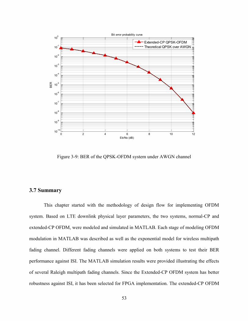
53
Figure 3-9: BER of the QPSK-OFDM system under AWGN channel
3.7 Summary
This chapter started with the methodology of design flow for implementing OFDM
system. Based on LTE downlink physical layer parameters, the two systems, normal-CP and
extended-CP OFDM, were modeled and simulated in MATLAB. Each stage of modeling OFDM
modulation in MATLAB was described as well as the exponential model for wireless multipath
fading channel. Different fading channels were applied on both systems to test their BER
performance against ISI. The MATLAB simulation results were provided illustrating the effects
of several Raleigh multipath fading channels. Since the Extended-CP OFDM system has better
robustness against ISI, it has been selected for FPGA implementation. The extended-CP OFDM
0 2 4 6 8 10 1210
-10
10-9
10-8
10-7
10-6
10-5
10-4
10-3
10-2
10-1
100
Eb/No (dB)
BE
R
Bit error probability curve
Extended-CP QPSK-OFDM
Theoretical QPSK over AWGN

54
system is modeled and simulated in Simulink using communication toolbox before
implementation using Xilinx System Generator. Following the design flow methodology, the
system will be implemented using Xilinx blocks as detailed in the following chapter.
55
Chapter 4
OFDM Hardware Design and FPGA
Implementation
As a part of System Editions of ISE® Design Suite, Xilinx System Generator for DSP is
a design tool as plug-in to Simulink that enables designers to design, simulate and develop High-
performance DSP systems. This design tool consists of Xilinx blockset, as Simulink library
which can be mapped directly into target FPGA hardware. Using Xilinx System Generator for
DSP, not only can DSP algorithms be designed and simulated, but also a synthesizable hardware
Description Language (HDL) code can be generated using HDL coder for Xilinx FPGAs.
Therefore Xilinx system Generator for DSP is considered a high-level tool for designing high-
performance DSP systems by providing system modeling and automatic HDL code generation
from MATLAB or Simulink.
Using Xilinx blockset libraries in model-based design environment Simulink does not
require previous experience of RTL design and Xilinx FPGAs since the downstream FPGA
implementation stages such as place, route and synthesis are automatically executed in order to
generate an FPGA bit file. Also Xilinx System Generator provides the functionality of
performing hardware co-simulation when a model-based design runs on Simulink and FPGA
[34].

56
In Chapter 3, it was described how MATLAB and Simulink were initially used to model
a QPSK-OFDM system including transmitter, channel and receiver. In this chapter the Simulink
model is transformed to hardware blocks using Xilinx System Generator. The Xilinx design is
then synthesized, mapped and routed to generate the bitstream to be downloaded into FPGA.
When hardware co-simulation is performed, MATLAB actually communicates with an FPGA
through an internal RAM.
Overview of each block used to design the transmitter, receiver or wireless channel is
given describing its functionality and specifications. The Xilinx blocks of OFDM transmitter,
wireless fading channel and receiver are introduced respectively. As the receiver blocks are
basically the inverse of the transmitter blocks, they are described briefly in this chapter.
4.1 Xilinx OFDM Transmitter
Figure 4-1: Block diagram of Xilinx OFDM transmitter
I I
Zero Padding1
Q Q
Zero Padding
In1
I
Q
QPSK Mapping
a
ba bz
-3
a
ba bz
-3
I in
Q in
I
Q
Sy n
IFFT
In
Gateway In1
I
Q
I
Q
CH I
CH Q
Fading Channel
sin
cos
CARRIER
Bernoulli
Binary
Bernoulli Binary
Generator1
a
ba + bz
-1
4
3
21
Sy stem
Generator

57
The OFDM transmitter is designed as shown in Figure 4-1. The data is generated from Simulink
environment and fed to the Xilinx design. The digital signal is modulated by baseband QPSK
modulator before it is modulated by FFT. Normally wireless channel model is applied to the
signal after it is up-converted. To apply multipath fading channel on a signal consists of I and Q
components, the components have to be separated as I and Q signals for complex multiplications.
For this reason, the multipath fading channel in our design is employed before modulating I and
Q signals. In this case, the design becomes more efficient and less sophisticated.
4.1.1 Random Data Generation
In model-based design, the random bits are generated using Bernoulli Binary Generator
provided by Communications System toolbox library as in Chapter 3. The input data is generated
with zero probability of 0.5 and sampling rate of 20 Mbps. Unlike the previous model in Chapter
3, the output of Bernoulli Binary Generator is sample-based output. To convert the input
Simulink integer, fixed-point or double data types to System Generator fixed-point type,
Gateway-In block is used to be as input for the Xilinx part of Simulink model. During the
process of conversion from float-point data type to fixed-point type, the Gateway-In block uses
some options for overflow and quantization. In the case of overflow, it can be used to saturate or
wrap the input value or flag it as an error. In fact, saturation is a process of converting
overflowed value to the largest positive or smallest negative value. Wrapping is to discard the
overflowed value, which are the bits to the left of the most significant bit. Flagging is just to
show an error whenever overflow occurs. Also Gateway-In block provides quantization options
of either rounding the value to the nearest representable value or truncating it by discarding the
bits right to the least significant bit [35].

58
4.1.2 QPSK Modulation
As shown in the figure below the QPSK modulator is implemented as a combination of
two ROMs and serial to parallel converter [36]. The serial to parallel block takes the serial
unsigned data represented in fixed point of one bit with zero binary point, and it creates a single
output of two consequential input bits. In other words it combines every two bits to be mapped
later in the ROM to the corresponding QPSK symbol. The serial input is ordered with the most
significant word first.
Figure 4-2: Xilinx QPSK modulator
Xilinx ROM block is a single port read-only memory that stores four words
corresponding to “00”, ”01” ,”10” and “11”. The values of the words are specified in the block
parameters as initial value vector. Since QPSK symbol consists of Quadrature and In-phase
values, two ROMs are used for both I and Q channels. They both have the same input and depth
but they are different in the initial value vector corresponding to QPSK constellation with gray
coding. To reduce the size of fixed-point representation, the power of QPSK symbol is not
normalized. As the Xilinx design is going to be downloaded to FPGA, the area of the design is
very important and has to be as small as possible. This area is affected by the number of bits used
ROM
ROM
2
Q
1
I
s pz-1
Serial to Parallel addr
addr
1
In1

59
in fixed-point representation. Therefore the QPSK In-phase and Quadrature values are set to be
either 1 or -1, to reduce the number of bits for their fixed-point representation.
4.1.3 Zero-Padding
Zero-padding in Xilinx design is not used for the same purpose as in MATLAB and
Simulink. Actually zero-padding is applied for up-sampling and creation of time space between
groups of QPSK symbols to form OFDM symbols. In fact these spaces are used for adding
Cyclic Prefix. In order to insert CP to OFDM symbol by using Xilinx IFFT block with pipelined
streaming input/output implementation mode, there must be a time space equal to the CP length,
so there will be no data loss during the transmission.
Figure 4-3: Xilinx zero-padding design
As shown in Figure 4-3, the zero-padding design is composed of Xilinx serial to parallel
and parallel to serial converters (SPCs), concat and constant blocks. First serial to parallel block
groups 1024 serial bits that represent 512 QPSK symbols with the most significant word first to
create a single unsigned output. Unsigned fixed-point representation with 256 bits is used to
represent a zero value as the output of constant block. Actually the number of unsigned Fixed-
point bits is related to the length of Cyclic Prefix. Since extended-CP OFDM system is
1
I
s pz-1
Serial to Parallel
p sz-1
Parallel to Serial
0
Constant
hi
lo}
Concat
1
I

60
implemented, the CP length is equal to one quarter of the OFDM symbol length. Therefore, the
time space between OFDM symbols needed to insert the CP is equal to the length of 128 QPSK
symbols. When the QPSK In-phase and Quadrature values are represented by two bits, 256 bits
are needed for each of I and Q values to represent 128 QPSK symbols. The unsigned outputs of
constant and S/P converter blocks are concatenated to create one bit vector of unsigned integer
number. The data input to hi port of the concat block occupies the most significant bits of the
output, while the data input to lo port occupies the least significant bits [35]. Therefore the output
of the concat block is an unsigned integer number represented by 1280-bit vector. This process
of uniting two inputs with the same bit rate creates one output with higher bit rate. In the parallel
to serial block, the input word is split into 640 parts, so every two bits form one signed word
with binary position at zero and the order of least significant bit first. As a result of zero-padding,
the bit rate of the output is higher than the input rate by ratio of 5/4.
4.1.4 OFDM Modulation
Since OFDM modulation can be implemented efficiently in hardware by using IFFT,
Xilinx IFFT 7.1 block is applied to design the OFDM transmitter that will be integrated and
verified into Xilinx Virtex-5. To choose a compatible IFFT block, the target Xilinx device has to
be defined first. As Virtex-5 FPGA ML506 board is used to verify the FPGA design, Xilinx
LogiCORE FFT V7.1 is designated since it is compatible with Virtex-5 FPGA. Xilinx FFT v7.1
block can be used either as FFT or IFFT depending on the block configuration. By implementing
Cooley-Tukey FFT algorithm, FFT V7.1 calculates DFT in an efficient way reducing processing
time and FPGA design area.

61
∑
∑
where
and N is FFT transform size.
In following sections, FFT v7.1 is overviewed and the theory of operation and configuration are
explained to give better and detailed understanding of OFDM modulation using IFFT v7.1.
4.1.4.A Overview of Xilinx FFT v7.1
Xilinx FFT v7.1 block supports Virtex-5 and other FPGAs such as Virtex-7, Virtex-6,
Virtex-5, Virtex-4, Spartana-6 etc. It computes forward and inverse DFT for N-point vector of
complex values. The size of FFT v7.1 can be from . The complex data input, and
, can be Fixed-point or Float-point numbers. As the FPGA area is limited, the real and
imaginary components of are represented in Fixed-point with as small number of bits as
possible without affecting the system performance. In other words the number of bits needed to
represent values is inversely proportional to FPGA area, as there are many mathematical
computations required for calculating DFT.

62
Figure 4-4: Xilinx FFT V7.1 block with unscaled output
However, each FFT real and imaginary input can be represented as 2’s complement with
number of bits in the range of 8 to 34 bits inclusive [35]. The FFT block uses either block RAM
or distributed RAM. The output order can be either bit/digit reversed or natural order.
4.1.4.B FFT Architecture
There are four architecture options in FFT v7.1 that are different in core size and
transformation time. The architectures are Radix-2 Burst I/O, Radix-4 Burst I/O, Radix-4 Lite
Burn I/O and Pipelined Streaming I/O [37]. Depending on the design speed and area, one of
these options is selected.
Pipelined, Streaming I/O is completely different than the other architectures since the
data is processed continuously, which is suitable when data input frames are coming
continuously in stream as in our OFDM system design. In Pipelined, Streaming I/O architecture,
many Radix-2 butterfly processing engines are pipelined to obtain the continuity of data
processing.
xn_re
xn_im
start
cp_len
cp_len_we
fwd_inv
fwd_inv_we
xk_re
xk_im
xn_index
xk_index
rfd
busy
dv
edone
done
cpv
rfs
Fast Fourier Transform 7.1

63
Memory
Radix-2 Butterfly
Memory
Radix-2 Butterfly
Input data
Xn
Stage 0 Stage 1
Group 0
Memory
Radix-2 Butterfly
Memory
Radix-2 Butterfly
Stage 2 Stage 3
Group 1
Memory
Radix-2 Butterfly
Memory
Radix-2 Butterfly Output Shuffling
Output Data
Xk
Figure 4-5: Pipelined Stream I/O Architecture
As shown in the figure above each Radix-2 has a memory block to store data that requires
more resources. These memories give the core the ability to perform multitasks simultaneously,
such as loading the next frame of data, calculating the transform on the current frame of data and
unloading the previous frame of data. As depicted in the architecture, every two Radix-2 stages
are grouped. In each group, the data is scaled when the scaled fixed-point mode is selected. As a
result the fixed-point mode is more sufficient using fewer resources than floating-point mode. In
Pipelined Stream I/O solution, the input data is provided in natural order, but the order of output
data can be natural or bit reserved. In our design, the output order is natural, although it requires
more memory.

64
4.1.4.C FFT v7.1 Configurations
To make FFT v7.1 work like OFDM modulator, some configurations have to be done
according to the specifications of OFDM design. As there are architecture options that offer a
trade-off between transform time and core size, the pipelined Stream I/O architecture is selected
for its ability of performing all the tasks simultaneously and data is processed continuously [37].
With the other architectures, FFT block cannot load the input data frame, compute the transform
and unload the output data frame in natural order. As in the extended-CP OFDM system
specifications, the FFT transform length is chosen to be 512, which is in the range of 8 to 65538
sample points that FFT block supports for Pipelined Streaming I/O implementation. Output
ordering is selected to be natural order, although it has an increase in memory used by the core.
Since the input data is in natural order, the natural mode is preferred so that input samples are
corresponding to output samples in the same order, and that is simpler and does not require bit
order revision in the receiver. The least significant bits of the data path at the output of butterfly
are required to be trimmed in each stage, and FFT v7.1 offers two options for rounding mode,
truncation and convergent rounding. The convergent rounding is applied in the OFDM
modulator design as truncation causes DC bias after the butterfly stages. To make FFT v7.1
insert the cyclic prefix in the output data frame as in OFDM modulation, the order of output data
has to be natural and Cyclic Prefix Insertion option is selected. As explained, there must be gaps
between the input data frames to allow the cyclic prefix to be added without losing information
data. Zero-padding is the solution used in our OFDM design to make time space between each
group of 512-QPSK symbols. Moreover, the input data frame has to be synchronized with FFT
block through FFT START signal which informs FFT block to begin data loading.

65
Figure 4-6: Xilinx OFDM modulator design
The cyclic prefix length is specified by the input port CP_len. As a result of selecting
cyclic option, the FFT output is composed of a copy of the last part of the output data followed
by the output data as explained in OFDM modulation. For fixed-point representation, the
precision is limited and that can introduce an overflow due to the arithmetic operations in each
butterfly stage. This overflow leads to an increase in the number of bits representing the output
value. To prevent overflow, FFT has an option of scaling in each butterfly stage according to
scaling schedule provided by the scaling input signal, SCHALE_SCH. For our OFDM system
design unscaled option is chosen due to the loss of data precision.
As experienced, scaling has a major effect on the system performance and the best way to
have high performance is to scale the output right after FFT block. Using Xilinx CMult block,
the scaling can be done as well as determining fixed-point precision. Since the input data vector
of complex values has to have a size in the range of 8 to 34, two CMult blocks with scale of 0.5
are applied to I and Q channels before FFT block to modify the number of bits in fixed-point
precision to 8 bits. As in DFT computation, the output of IFFT has to be divided by the size of
3
Syn
2
Q
1
I
Terminator7
Terminator6
Terminator5
Terminator4
Terminator3
Terminator2
Terminator1
Terminator
xn_re
xn_im
start
cp_len
cp_len_we
fwd_inv
fwd_inv_we
xk_re
xk_im
xn_index
xk_index
rfd
busy
dv
edone
done
cpv
rfs
Fast Fourier Transform 7.1 128
Constant4
0
Constant3
1
Constant1
x 0.003906
CMult3
x 0.003906
CMult2
x 0.5
CMult1
x 0.5
CMult
2
Q in
1
I in

66
IFFT, which is 512 in our case. The output of FFT v7.1 is scaled with 1/256 since the input data
is already scaled with ½. However, the Xilinx constant blocks with constant values of 0 and 128
are utilized to indicate operation type forward or inverse FFT and specify the CP length,
respectively. Also the control signal, such as START, CP and Forward-inverse Write Enable
signals, can be provided by Xilinx constant block of true Boolean value. As depicted in Figure 4-
6, “edone” signal is used for synchronization purpose between the OFDM modulator and
demodulator.
4.1.5 Digital Up-Conversion
To convert a complex digital signal centered at zero frequency to a digital real signal
centered at intermediate frequency, a digital up-converter (DUC) is designed using Xilinx DSP
blockset library. First two digital high-frequency signals, Sine and Cosine, are generated using
Xilinx DDS Compiler 4.01 block. Actually these digital signals are the carrier signals with phase
difference of π/2 and they are used for up conversion of I and Q baseband signals to RF signals.
Figure 4-7: Carrier signal generator
2
cos
1
sin
sine
cosine
DDS Compiler 4.0 1
z-1
x 1
CMult1
z-1
x 1
CMult

67
The Xilinx DDS compiler 4.01 is a direct digital synthesizer that uses Lookup table
scheme to generate sinusoids. The direct digital synthesizer generates a phase by digital
integrator and then maps it to the lookup table to produce the output waveform. The phase
increment and offset can be set dynamically through optional input ports or can be defined as
constant [35]. For our design, the phase increment and phase offset are constant since there is no
need to change the phase of carrier signal. The Xilinx DDS compiler is configured to generate
sine and cosine signals that have 25 MHz with zero phase offset. Since the system clock
frequency of ML506 board is 100 MHz, the outputs of DDS compiler block are periodic signals
of values [0,-1,0,1] and [1,0,-1,0] for the sine and cosine output ports respectively. To optimize
the FPGA area needed for the carrier signal generator design, two CMult1 blocks are utilized to
resize the fixed-point precision for DDS compiler output. Therefore a Fixed-point of 16-bit
width is the new representation of digital carrier signal generator output.
Using two Xilinx multipliers, Mult4, the two sine and cosine digital signals are then
multiplied with Quadrature and in-phase signals coming out from fading channel design as
shown in the figure of OFDM transmitter design. The Xilinx Mult4 block implements a
multiplier that computes the product of two input data. Each Mult4 multiplier has a delay of 3
clock cycles as default setting but fixed-point precision is defined for area optimization. The
delay of Mult4 block means that the Mult4 block takes 3 sample periods to show its output of
production.

68
Figure 4-8: I and Q Xilinx digital modulator and up-converter
As depicted in the figure, the output of two Mult4 block are fed to Xilinx AddSub block
that is specified to do addition operation with output of 18-bit fixed-point representation and
signed arithmetic type. All Mult4 and AddSub blocks in I and Q digital modulator are configured
for truncation and wrapping for quantization and overflow operation respectively. Not only does
the above Xilinx design combine I and Q signals to be in one channel, but it also up-converts
them at intermediate frequency of 25 MHz with sampling rate of 100Msps. Actually the
sampling period is equal to an integer number of clock cycles, so the maximum sampling rate
that can be provided in ML506 is equal to the clock frequency of the board.
4.2 Rayleigh Fading Channel
As explained in the previous chapter, a Rayleigh fading channel can be modeled by
generating the real and imaginary components according to independent zero-mean Gaussian
processes. The same methodology used in MATLAB source code is applied to design Xilinx
Rayleigh fading channel. To generate a Rayleigh fading channel that has magnitude and phase
distortions, a multipath fading channel is modeled using several Xilinx blocks. The first step that
has been taken is to design an independent fading noise generator for each path of the fading
3
a
ba bz
-3
a
ba bz
-3
sin
cos
CARRIER
a
ba + bz
-1
2
Q
1
I

69
channel. Every fading noise generator has two independent white Gaussian noise generators as
shown in the figure below.
Figure 4-9: Xilinx fading noise generator
The White Gaussian Noise Generator block generates white noise using Box-Muller
algorithm and the center limit theorem [38]. The number of initial seeds for each White Gaussian
Noise Generator has to be specified. To make output variables of White Gaussian Noise
Generators independent, the number of initial seeds of each White Gaussian Noise Generator has
to be different from each other. Since the power of the complex fading noise has to be
normalized, the outputs of White Gaussian Noise Generators that create real and imaginary parts
are multiplied by 1/√ . This can be done using Xilinx CMult block with gain of √ . The
output of CMult is defined to have signed 16-bit fixed-point representation.
To create a Rayleigh fading channel that has three paths, three Xilinx fading noise
generators are required to generate three complex random independent variables to be multiplied
2
Out2
1
Out1
reset noise
White Gaussian
Noise Generator1
reset noise
White Gaussian
Noise Generator
0
Constant1
x 0.707
CMult2
x 0.707
CMult1

70
by OFDM signals. For simplicity, one fading channel path is discussed demonstrating the
sections of Rayleigh fading channel model.
Figure 4-10: The first path of Xilinx 3-paths Rayleigh fading channel design
As fading noise generator has random output with sampling rate of 100/640 Msps and
OFDM sampling rate is 100/8 Msps, the fading noise generator output has to be down-sampled 8
times to get a random signal with sampling rate of 100/(640x8) Msps. In other words, the fading
channel has to be static for each OFDM symbol, which is equal to 640 samples including the
cyclic prefix. The I and Q input signals are delayed to be synchronized with the random complex
noise. Since all Xilinx blocks start working concurrently, the OFDM symbol has to be delayed to
match the random fading noise generated according to the coherent time of fading channel. As
designed in MATLAB source code, the coherent time of fading channel is equal to OFDM
symbol period. The wireless channel is modeled using the exponential model discussed in
Chapter 3. The power is different for each path and decreases exponentially according to the
I
Q2
Q
1
I
Out1
Out2
fading noise generator
z-1
8
Down Sample1
z-1
8
Down Sample
z-138
Delay5
z-138
Delay2
ar
ai
br
bi
pr
pi
Complex Multiplier 3.1 1
x 0.7117
CMult2
x 0.7117
CMult1
2
Q
1
I

71
power delay profile of the exponential model. The power of each path has to be calculated in
order to obtain the gain of each path.
Using the discrete-time power delay profile equation, the total normalized power is 0.9872 for
, and therefore the normalized power for the three paths P(0), P(1) and P(2) are equal
to 0.5065, 0.3072 and 0.1863 respectively. By determining normalized path gains for the three
paths, the normalized signal gains or factors can be defined according to the relationship
between the voltage and the power. Since
and √ , then √
√
As a result, the signal factors of the 1st, 2nd and 3rd paths are 0.7116, 0.5543 and 0.4317.
To apply the signal factors, two Xilinx CMult blocks with fixed-point precision of 18 bits are
utilized for each path as a gain operator. Each pair of CMult blocks applied on I and Q channels
has the same constant value equal to the signal factor for the specified path. To apply the phase
and magnitude channel distortion on the OFDM complex signal, a Xilinx Complex Multiplier is
required for each path. It has four input ports; two for real and two for imaginary components.
The complex output of Xilinx Complex Multiplier is added to other complex output using Xilinx
AddSub blocks. The real output values are then summed separately from the imaginary values.
As a result, four Xilinx AddSub blocks are utilized to obtain the summation of three complex
outputs. The Xilinx AddSub blocks are configured with 18-bit fixed-point representation giving
high precision with negligible data loss.

72
4.3 AWGN Channel
To test the performance of OFDM system, white Gaussian noise is added to the up-
converted OFDM signal. This noise makes errors in the received information bits after the
received OFDM signal is demodulated and demapped. By comparing the original information
bits sent and the information bits received, the number of errors can be defined and the error rate
is calculated. In order to calculate error ratios, the simulation runs many times. Each time,
different ratio of bit energy to noise power spectral density is applied to white Gaussian noise.
According to the error ratios, the BER curve can be drawn using MATLAB function. The BER
shows QPSK-OFDM system performance compared with the theoretical QPSK BER.
To generate white Gaussian noise that has specific power according to several ratios of
bit energy to noise power spectral density ( ), the Signal to Noise Ratio is imported from
the workspace every time the simulation runs. Therefore a MATLAB source code is written to
calculate SNR values according to . It also runs the Simulink model and saves the number
of information bits and errors in matrices. On the other hand, the Simulink model-based design
imports from the workspace and exports the number of information bits and errors to the
workspace. In other word, there is a data exchange between the Simulink model and the
MATLAB workspace in order to test the OFDM design under different
In order to generate white Gaussian noise, Xilinx White Gaussian Noise Generator block
is utilized for modeling AWGN channel. With frequency equal to the clock frequency, the output
of Xilinx White Gaussian Noise Generator block is going to be multiplied with using
Xilinx Mult block as depicted in Figure 4-11.

73
Figure 4-11: AWGN channel Design
Since the value is imported from workspace through Simulink constant block,
Gateway-In block is placed between Xilinx portion and Simulink constant block. Gateway-In
block converts Simulink float-point or fixed-point data types to System Generator fixed-point
data type according to the block configuration. The Gateway-In block is configured to have
output of 16-bit fixed-point data type with rounding in quantization and saturating operation in
overflow process. For better accuracy, the fixed-point type for the output of Xilinx Mult block
has 18-bit width, which is more than the number of bits for the input fixed-point data type. After
white Gaussian noise is generated with specific power, it is added to the up-converted OFDM
signal using Xilinx AddSub block. Xilinx AddSub block performs addition operation with 2
clock cycles latency and the same fixed-point representation of the input.
4.4 Xilinx OFDM Receiver
The receiver performs the inverse process of the transmitter in communications system.
The main receiver blocks are briefly described in this section. The QPSK-OFDM transmitter and
receiver are implemented in the same FPGA. The receiver is designed with assumption of perfect
1
Out
reset noise
White Gaussian
Noise Generator
a
ba b
z-3
Mult
In
Gateway In2
-C-
Es/No
0
Constant
a
ba + bz
-2
AddSub
1
In

74
synchronization between the transmitter and the receiver. First stage of the receiver is to down-
convert the received OFDM signal as shown in Xilinx OFDM receiver below.
Figure 4-12: Xilinx QPSK-OFDM receiver
4.4.1 Down-Conversion and OFDM Demodulation
Another Xilinx carrier signal generator with the same design in the transmitter is applied
in the I & Q demodulator. In order to extract out In-phase and Quadrature signals, digital sine
and cosine signals are generated with the same frequency of 25 MHz and sampling frequency of
100 MHz. To match the phase of sinusoidal signals with the received OFDM signal, two Xilinx
delay blocks are applied to the sinusoidal signals before they are multiplied with the OFDM
signal. One clock cycle delay is equal to 45 degree phase change since the sampling period is
equal to one quarter of signal time period . Therefore the sinusoidal signals are delayed with
number of clock cycles in the range of 0-3 inclusive. As previously explained, the In-phase
component of OFDM signal can be retrieved by multiplying the up-converted signal with cosine
edoneH(f)
In1Out1
Puncturing1
In1Out1
Puncturing
I in
Q in
Ch I
Ch Q
I
Q
Phase Noise Cancellationa
ba b
z-3
a
ba b
z-3
Out
Gateway Out2
Out
Gateway Out1
I in
Q in
In3
I
Q
FFTz
-2
8
Down Sample1
z-1
8
Down Sample
z-2
Delay5
z-2
Delay2
I
Q
Out1
De-Mapping
I
Q
Sy n
Ch I
Ch Q
Channel istimation
sin
cos
CARRIER1
InO
ut
AWGN Channel

75
signal that has the same frequency and phase of the carrier signal. Also the received OFDM
signal is multiplied by sine signal in order to recover the quadrature component.
To down sample the I and Q digital signals that have sampling rate equal to the clock
frequency, two Xilinx Down Sample blocks are placed right after the Xilinx multipliers. Xilinx
Down Sample block samples the input signal by taking either the first or the last value of a frame
and holding it on the output until the next sample is taken. The ratio of output sample period to
the input is called the sampling rate. Our objective is to down sample the received OFDM signal
from 100M samples/Sec to 12.5 M samples/sec, so the sampling rate is chosen to be 8. After
down sampling, the OFDM signal is ready to be demodulated using Xilinx FFT v7.1 block.
In the receiver side, the Xilinx FFT v7.1 is configured to perform a Fast Fourier
Transform. Synchronization between Xilinx IFFT block in the transmitter and Xilinx FFT block
in the receiver is done in order to define the first sample of each OFDM symbol. In fact, the
“edone” signal of Xilinx FFT block goes high one clock cycle before the transform calculation is
completed and data output is unloaded through and output ports. Therefore, the
edone output port of IFFT block in the transmitter is connected to the START input port of the
FFT block in the receiver, but the edone signal is delayed to match the first sample of OFDM
symbol arriving Xilinx FFT. However, the output of Xilinx FFT block consists of demodulated
OFDM symbol and CP of the symbol. The CP is considered here as extra data that is going to be
removed later by puncturing.
4.4.2 Phase Noise Cancellation
In multipath fading channel, the amplitude of transmitted signal is distorted as well as the
phase. To be able to recover the original signal, the channel response ( ) has to be estimated

76
using some algorithms to cancel the channel distortion. In our OFDM design, the channel state
information is assumed to be known. To do that, the channel response ( ) is created according
to the complex path gains generated in the fading channel. In the fading channel section, three-
path Rayleigh fading channel is modeled using the exponential model and implemented through
Xilinx blocks. The OFDM faded signal can be expressed as
( ) ( ) ( ) ( )
where ( ) is transmitted OFDM signal, ( ) is the channel impulse response and ( ) is
OFDM received signal. By applying Fourier transform on the above equation
( ) ( ) ( )
( ) ( )
( )
where Y( ) is the frequency response of distorted OFDM signal, ( ) OFDM demodulated
signal and ( ) is the channel frequency response. Since the OFDM signal is demodulated using
fast Fourier Transform, ( ) is actually the output of Xilinx FFT block which can be found if
( ) is known. To apply this method to cancel the channel distortion in our OFDM system
design, first the channel impulse response ( ) has to be created with the same time period of
OFDM symbol. Using time division multiplexer blocks, the channel impulse response ( ) is
created according to the three path gains of fading channel. Zero-padding technique is applied
for creating both real and imaginary channel response components that stay constant during the
entire OFDM symbol and changes randomly from one OFDM symbol to the next. Two Xilinx
Time Division Multiplexer blocks and two Xilinx Constant blocks are utilized to constitute ( )
from the three complex path gains and zeros. As depicted in Figure 4-13, the first Multiplexer

77
combines 32 input signals that have sampling period of 5120 clock cycles, which is equal to
OFDM symbol period. The output of Xilinx Time Division Multiplexer 1 has rate of 32xR where
R is the rate of the input signals. Therefore, the sampling period of the first multiplexer is
5120/32 = 160 clock cycles, and for second multiplexer the sampling period is 160/20= 8 clock
cycles.
Figure 4-13: Xilinx design for the real component of channel response
The reason of using two Xilinx Time Division Multiplexer blocks is that the maximum number
of input ports for Xilinx Time Division Multiplexer is 32 inputs which are not enough to create
( ) with 640 samples.
1
h(t)
d0d1d2d3d4d5d6d7d8d9d10d11d12d13d14d15d16d17d18d19
qTDM
Time Division
Multiplexer2
d0d1d2d3d4d5d6d7d8d9d10d11d12d13d14d15d16d17d18d19d20d21d22d23d24d25d26d27d28d29d30d31
qTDM
Time Division
Multiplexer0
Constant1
0
Constant
3
Gi3
2
Gi2
1
Gi1

78
In order to calculate ( ) from ( ), Xilinx FFT v7.1 is also applied. Since there is no
Xilinx complex divider in the Xilinx blockset library that can divide two complex signals, the
following Xilinx complex divider is designed using Xilinx Coordinate Rotation Digital
Computer (CORDIC) Dividers, Complex Multipliers, Mults, AddSub and invertor blocks. Two
Xilinx delay blocks are utilized to delay the channel frequency response I&Q signals in order to
match the demodulated OFDM signal.
Figure 4-14: Xilinx Complex Divider Design
This complex divider design is based on simple arithmetic operations for dividing two
complex numbers that is defined in terms of complex multiplication and real division. The Xilinx
CORDIC Divider uses a fully parallel Coordinate Rotation Digital Computer algorithm in Linear
Vectoring mode [39]. The output of Xilinx CORDIC Divider in the Xilinx complex divider
design has a fixed-point representation of 20-bit width and 14 binary bits.
2
Q
1
I
a
ba b
z-3
Mult1
a
ba b
z-3
Mult
not
Inverter
z-143
Delay3
z-143
Delay1
ar
ai
br
bi
pr
pi
Complex Multiplier 3.1 2
x
y
div z-35
x
y
y/x
CORDIC DIVIDER2
x
y
div z-35
x
y
y/x
CORDIC DIVIDER1
a
b
a + bz
-3
AddSub
4
Ch Q
3
Ch I
2
Q in
1
I in

79
4.4.3 Puncturing
The demodulated OFDM signal has to be punctured to remove the cyclic prefix which is
considered as redundant data. By using a large number of bits in fixed-point representation, the
demodulated OFDM or QPSK signal can’t be punctured due to the limited number of bits that
Xilinx Serial to Parallel block can accept. To solve this problem and optimize the OFDM system
design in term of area, each of I and Q QPSK signals is de-mapped to [1,-1] values to reduce the
number of bits to two bits only. To de-map the demodulated OFDM signal, Xilinx bit slice
extractor and single port ROM are utilized. The Xilinx slice block in this design extracts only the
sign bit from every input sample and represents it at the output. The Xilinx ROM block with
initial value vector [1, -1] receives one bit for the memory address of initial value. In other
words, the output of Xilinx ROM block is either 1 or -1 according to the input 0 or 1
respectively.
Figure 4-15: Xilinx Puncturing Design
Since all Xilinx design blocks start working concurrently, Xilinx delay block is applied in
puncturing design in order to match the first bit of the demodulated OFDM symbol in the I and Q
channels with the first bit of 1280 bits that Xilinx Serial to Parallel block groups in the
puncturing design. As the output of ROM block is represented with 2-bit fixed-point, 1280 serial
bits are representing 640 samples including the cyclic prefix. Xilinx Slice block with 1024-bit
width punctures these 640 samples to result in 512 samples. Finally the 1024 bit group is
1
Out1
[a:b]
Slice1
[a:b]
Slice
sp z-1
Serial to Parallel
addrz-1
ROM
ps
Parallel to Serial
z-595
Delay1
1
In1

80
converted back to be 512 samples, each group of two bits representing one sample. This Xilinx
puncture design is applied on both I and Q channel to remove the redundant bits and reduce the
sampling rate from 12.5 Msps to 10 Msps.
4.4.3 QPSK Demodulation
In Xilinx QPSK demodulator design, the Slice block is used to extract the sign bit from
the I and Q signals as in puncturing design. The two bits coming from I and Q channels are
concatenated to compose unsigned value by using Xilinx Bus Concatenator. The Xilinx ROM
block takes 2-bit unsigned number as the address of initial vector to present one of the symbols
[0, 2, 1, 3] in the output. The initial vector is a look-up table (LUT) stored in Xilinx ROM block.
Each symbol of ROM block output becomes two serial bits through Xilinx Serial to Parallel
block.
Figure 4-16: Xilinx QPSK demodulator
As a result, the input QPSK symbols are demapped according to the QPSK mapping scheme
used in the transmitter, and the output sampling rate is doubled since one I or Q sample leads to
two serial samples or bits in the output.
ROM
1
Out1
[a:b]
Slice1
[a:b]
Slice
addrz-1ps
Parallel to Serial
hi
lo}Concat
2
Q
1
I

81
4.5 Summary
In this chapter, the Xilinx design for extended-CP OFDM system was described
including the functionalities and configurations of each Xilinx block. Starting with the
transmitter, the Xilinx QPSK modulator, zero-padding and IFFT were discussed in detail. The
OFDM signal is up-converted to IF of 25 MHz utilizing I and Q modulator. To demonstrate the
OFDM resistance to frequency-selective fading, 3-path fading channel was modeled and
implemented based on the exponential wireless channel model. As it has been implemented in
MATLAB in Chapter 3, the channel model consists of six independent Gaussian noise
generators, two generators for each path. The phase noise was cancelled in the receiver side with
pre-knowledge of the channel state information. As the whole OFDM system including the
wireless channel was implemented on the same FPGA, there was no need for carrier recovery
system.
Overall this Xilinx design has a throughput of 20 Mbps with clock frequency of 100MHz.
In this design, transmitter, receiver and wireless channel are implemented. To verify the design,
the hardware co-simulation is performed and the test results are demonstrated in the next chapter.

82
Chapter 5
Hardware Verification and Test Results
The Xilinx OFDM system model (explained in Chapter 4) is created for FPGA
implementation by using high-level components from Xilinx-specific blockset libraries. The
Xilinx OFDM model is first simulated using Simulink and System Generator to verify the
functionality of the system. Using HDL Coder and System Generator for DSP together, VHDL
code can be automatically generated from Simulink model for Xilinx FPGAs. In fact, the Xilinx
OFDM model is compiled to an HDL netlist, which can be synthesized and implemented with
Xilinx ISE Design suite. System Generator also provides hardware co-simulation by making the
Xilinx design running in an FPGA. To verify our Xilinx OFDM design, hardware co-simulation
is performed using a DSP development kit, Virtex5 ML506 board. Xilinx FPGA DSP
development kits are usually used for signal processing and communications designs, due to their
rapid implementation of Simulink models. In this chapter, the results obtained from the
simulation in Simulink and the hardware co-simulation are discussed and analyzed. Also
overview of Virtex5 ML506 board is given as well as hardware co-simulation steps.
5.1 The Simulation Results of Xilinx OFDM System
Using Xilinx System Generator tools, the simulation phase was done to test the Xilinx
OFDM design and evaluate the results before hardware co-simulation. The result of hardware co-
simulation is also shown in this section.

83
As elucidated, random binary numbers are generated by Bernoulli Binary Generator in
Simulink and converted to Xilinx fixed-point through Gateway In. As Xilinx QPSK modulator is
described in the previous chapter, the random input bits are modulated according to the QPSK
scheme. The modulator has two output channels to represent In-phase and Quadrature
components of QPSK symbols depicted in Chapter 2. To make the QPSK symbol compatible
with IFFT block, zeros are padded between groups of QPSK symbols as illustrated in Figure 5-1.
Figure 5-1: In-phase component of zero-padding output
The QPSK symbols are modulated using IFFT block to create OFDM signal represented in 16-
bit fixed point representation. The frequency spectrum of baseband OFDM signal is shown in
Figure 5-2.
500 1000 1500 2000-1.5
-1
-0.5
0
0.5
1
1.5
Clock cycles
Zero
-paddin
g o
utp
ut
for
I channel

84
Figure 5-2: OFDM signal spectrum
As depicted, the OFDM signal has a bandwidth of 12.5 MHz, which is in the range of -
6.25 and +6.25MHz. The input bitrate of the OFDM system is 20 Mbps. and after QPSK
modulation, the bitrate of the signal is changed to 10 Mbps for I and Q channels. Due to zero
padding or up-sampling, the bitrate of QPSK signal increases to 12.5 Mbps. Xilinx IFFT block
converts serial data to parallel data before the transform process in such a way that one stream of
QPSK symbols is converted to 512 parallel streams. Therefore, the bitrate of the QPSK signal is
divided by 512 to become 12.5/512 Mbps for each parallel sub-signals. By preserving the
orthogonality, the parallel QPSK sub-signals are then modulated using IFFT to create an OFDM
signal with 12.5 MHz bandwidth.
The I and Q OFDM signals are modulated and up-converted using the Xilinx I&Q
modulator to be transmitted in the same channel. By passing the multi-path fading channel, the
signal is distorted in phase and amplitude before it arrives the receiver.

85
In the receiver side, the signal is down-converted by I & Q demodulator and then
demodulated using FFT block but it still has noise in amplitude and phase. To remove the phase
distortion from the received signal, it is fed to the phase cancellation subsystem with pre-
knowledge of the channel state information. The output of the phase cancellation subsystem is
punctured to remove the zeros added in the transmitter. This process is actually down sampling
the signal from 12.5 Mbps to 10Mbps. The last stage in the receiver is to demodulate the QPSK
signal. Finally, the output data of the Xilinx portion running on the FPGA is compared with the
input data in the Simulink environment to calculate the ratio between number of errors and the
original data. This ratio is stored in MATLAB workspace to draw the BER curve.
5.2 Hardware Co-Simulation
Simulink environment provides a graphical environment and block libraries. This allows
engineers to design, simulate, implement and test dynamic and embedded systems used in many
applications such as signal processing and communications. By generating synthesizable VHDL
code using Simulink HDL Coder, a Model-based Design in Simulink can target FPGAs.
However, Xilinx System Generator is a high-level tool for designing high-performance DSP
systems using FPGAs. Using Xilinx library of bit-and cycle-true blocks, engineers can build a
model in Simulink that targets Xilinx FPGAs specifically [40]. Based on Xilinx model, a
synthesizable HDL code can be automatically generated by employing Xilinx System Generator
for DSP. Moreover, Xilinx System Generator provides hardware co-simulation, in such a way
that Xilinx design running in an FPGA is incorporated into Simulink design. During the
compilation of hardware co-simulation, a bitstream is created for each Xilinx block, so the
compiled portion is ready to be downloaded into an FPGA [40]. When the simulation starts in
Simulink, the compiled portion runs in the FPGA to calculate output results. In other words,

86
there will be a data exchange between the Simulink environment and FPGA board. As a result,
the Xilinx OFDM design is tested and verified in actual hardware. Moreover, the hardware co-
simulation can speed up the simulation when some portions of the applications are executed as
software program, while the other portions are executed in hardware. The hardware co-
simulation for Xilinx OFDM design verification has been done using XtremeDSP development
platform -Virtex-5 FPGA ML506 Edition and PC with the software requirements; MATLAB,
Simulink, Xilinx System Generator and ISE Design Suite.
5.2.1 Introduction of XtremeDSP board
To implement the Xilinx OFDM design, the Virtex-5 FPGA ML506 is used as a
development platform for our experimentation. Actually the Virtex-5 family of FPGAs offers
multiple platforms with high-performance logic, signal processing, serial connectivity and
embedded processing resources [34]. XtremeDSP development platform -Virtex-5 FPGA
ML506 Edition is designated for hardware co-simulation due to the feathers of Virtex-5 family.
Figure 5-3: XtremeDSP development platform -Virtex-5 FPGA ML506 Edition

87
The features of ML506 board are demonstrated below [41].
Xilinx Virtex-5 FPGA
Two Xilinx XCF32P Platform Flash Programmable Read Only Memories (PROMs) (32
Mb each) for storing large device configurations.
Xilinx System ACE™ CompactFlash configuration controller with Type I CompactFlash
connector to program the FPGA through the JTAG port.
64-bit wide, 256-MB Double Rate Data Small Outline Dual In-line Memory Module
(DDR2 SODIMM)
Clocking
Programmable system clock generator chip
The ML506 board provides a programmable clock generator device to generate
different clock to FPGA and the board peripherals.
25 MHz to the Ethernet PHY
14 MHz to the audio codec
27 MHz to the USB Controller
33 MHz to the Xilinx System ACE CF
33 MHz, 27 MHz, and a differential 200 MHz clock to the Xilinx FPGA
100-MHz crystal oscillator socket
This clock signal is connected to the FPGA clock pin
External clocking via SMAs (two differential pairs)
The ML506 allows the designers to use external clock source to drive differential
clock signals through 50-Ohm SMA connectors to be the global clock input to the

88
FPGA. Also differential clock signal can be driven from FPGA to an external
device through the SMA connectors.
General-purpose active-high DIP switches (8) connected to the I/O pins of the FPGA,
LEDs (8) for general purpose usage, active-high pushbuttons, and rotary encoder.
Expansion headers
Single-ended expansion head contains 32 connections to the FPGA
input/outputs.
Differential expansion header contains 16 pairs of differential signal I/O
connectors.
Additional I/O 14 pins shared with pushbutton switches and LEDs,
power, JTAG chain expansion capability, and IIC bus expansion.
RS-232 serial port allowing the FPGA to communicate with external devices.
16-character x 2-line LCD to display text information.
8-Kb EEPROM to store temporary data and IIC bus utilized for adding IIC devices and sharing
the IIC controller in the FPGA.
JTAG configuration port for programming the FPGA with the use of Parallel Cable III,
Parallel Cable IV, or Platform USB download cable.
10/100/1000 Tri-Speed Ethernet PHY, USB Controller with Host and Peripheral Ports.
Since ML506 board offers easy way to setup and high speed I/O connectors, the ML506 board is
employed for JTAG hardware co-simulation of OFDM design using Xilinx parallel cable IV to
connect the PC to the JTAG port [42].

89
5.2.2 Hardware Co-Simulation Setup
In order to perform hardware co-simulation, many steps have to be taken before co-
simulating a Xilinx model-based design. These steps depend on the type of hardware co-
simulation and FPGA boards. As the ML506 is utilized for testing the OFDM system design,
specific instructions for ML506 are provided as following:
A. ML506 board Setting up for JTAG Hardware Co-Simulation.
The ML506 board should be connected in the lab according to the document from
Xilinx, ML505/506/507 Overview and Setup [43]. To configure the board for hardware
co-simulation using the JTAG port, the DIP switches for configuration address are set up
to “101” state. Figure 5-4 illustrates the JTAG chain of the ML506 board [41].
Platform
Flash
Memory
U4
CPLD
U3
System ACE
Controller
U2
PC
4
Co
nn
ce
tor
J1
Platform
Flash
Memory
U5
FPGA
U1
Expansion
J5
Ju
mp
er
J2
1
Figure 5-4: JTAG chain
As shown in JTAG chain the data is transferred from PC connector through
Platform memories, CPLD and system ACE controller to FPGA, and then from the
FPGA back to System ACE controller with extension option defined by the jumper J21.
Using the JTAG chain, not only can the FPGA be programmed but also the CPLD and

90
the Platform Flash PROMs. PC4 JTAG connection allows a host computer to program
the FPGA by downloading bitstream to the FPGA using iMPAC software tool. The
FPGA can also be programed by the system ACE controller when CompactFlash card is
inserted and some configurations are done on address configuration DIP switches. In fact
there are 8 DIP switches in SW3. The first three switches (1-3) are to set the
configuration address, and the next three (4-6) to set the mode of configurations, and the
last two switches (7-8) are to enable or disable the Platform Flash PROM Fallback and
System ACE controller. For JTAG hardware co-simulation, the configuration address
DIP switches are set to “00010101”.
B. Model Compilation for Hardware Co-Simulation
The second step is to compile the Xilinx OFDM design into hardware using the
System Generator block, which determines the compilation type. To configure the
System Generator block, the compiling target has to be defined by selecting the
appropriate compilation type, which is in our case hardware co-simulation, and the target
FPGA board. Using the code generator in System Generator, a FPGA configuration
bitstream for Xilinx model is generated. During the compilation process System
Generator generates the HDL and Netlist files for the Xilinx model as well as running the
downstream tools for the production of FPGA configuration bitstream. In fact the FPGA
configuration file contains the hardware of Xilinx model and interfacing logic for the
communication process between System Generator on the PC and the Xilinx design
running on an FPGA. In this case the System Generator can write values to input ports of
the Xilinx design and read values from output ports through the physical interface.

91
C. Hardware Co-Simulation Blocks
As a result of compiling the Xilinx model into an FPGA bitstream, a new
hardware co-simulation block is created in a new Simulink library by System Generator.
This hardware co-simulation block has the same number and names of ports for the
original Xilinx design or model. By copying the hardware co-simulation block to other
Simulink and system generator, it can be used as a Simulink block but during the
simulation the hardware co-simulation block interacts with the FPGA board. Many
processes of data transfers, clocking and device configuration are done during the
hardware co-simulation.
For the OFDM design, a new Simulink model is created to test the JTAG hardware co-
simulation OFDM design block as shown in the figure below.
Figure 5-5: OFDM model for hardware co-simulation
Gateway In1
Gateway In2
Gateway Out1JTAG
Co-sim
OFDM Design
hwcosim
Error Rate
Calculation
Tx
Rx
Error Rate
Calculation2
Var
Constant2
Bernoulli
Binary
Bernoulli Binary
Generator1
Sy stem
Generator

92
D. Hardware Co-Simulation Clocking
Since Xilinx ML506 board is used for hardware co-simulation, the clock
frequency can be chosen to be equal or less than the system clock of the board. The
System Generator block gives 4 options for the clock frequency; 100, 66.7, 50 or
33.3MHz [44]. After setting the target clock frequency, which is 100MHz for our
experiment, the clocking mode has to be configured as well. Actually there are two
clocking mode, single-step and free running clock modes. In free-running clock, the
hardware clock runs continuously inside the FPGA and it is not related to the simulation
in Simulink. Also FPGA I/O ports are not synchronized with the event in Simulink. In
single-step mode, the FPGA clock is provided by Simulink to the hardware. In other
words, the hardware is kept in lock according to the simulation steps. As the hardware
receives a single clock for each simulation cycle, the hardware co-simulation block is
considered bit-true and cycle-true to the original model. Unlike Free-running clock mode,
the FPGA port input and output in single-step clock mode is synchronized with the events
in Simulink. For the co-simulation of OFDM design, single-step mode is applied by
selecting the clocking mode for the hardware co-simulation block before running the
hardware co-simulation.
5.3 Hardware Co-Simulation Results
Since accurate BER performance evaluation is crucial for the successful design, the BER
performance of the OFDM system in hardware is shown in this section. To draw the BER vs
curve, the system is co-simulated with nine different values of the ratio of bit energy to

93
noise power spectral density . In each point the system is running on the FPGA and output
data is compared with the input data in Simulink until the number of errors reaches . By
changing the noise power of AWGN, the ratio of is changed providing multiple values or
points to test the system at. The results at each test point are stored in MATLAB workspace. The
BER curve of the co-simulation is compared with theoretical QPSK modulation over Rayleigh
flat fading as shown in Figure 5-6. The hardware co-simulation is done using 18bit fixed-point
representation which is almost matching the theoretical QPSK curve. Actually system
performance in hardware co-simulation is similar to the simulation results using Simulink and
Xilinx System Generator. However, the BER performance gets worse if the number of bits for
fixed-point representation decreases.
Figure 5-6: BER comparison between hardware co-simulation and theoretical curves
0 5 10 15 20 25 30 35 4010
-5
10-4
10-3
10-2
10-1
100
Eb/No (dB)
BE
R
Bit error probability curve
Hardware co-simulation OFDM curve
Theoretical QPSK curve over flat fading

94
5.4 Hardware Utilization
As high-performance logic fabric, the Virtex-5 family provides powerful features to address
the needs for advanced logic designs. Using these feathers, such as the second generation 25x18
DSP slices, 36-Kbit block RAM/FIFO and SelectIO technology, the logic designer can build an
FPGA-based system with high performance and functionality. In fact, there are five Virtex-5
platforms; LXT, SXT, TXT and FXT. The Virtex-5 XC5VSX50T is used to implement the
OFDM system. This Xilinx device has 8160 Virtex-5 Slices, 288 DSP48E slices, 6 Clock
Management Tiles (CMT), 132 36-Kb block RAM blocks and distributed RAM of 720 Kb max
[45]. The Virtex-5 slices and distributed RAMs are the basic logic elements for Xilinx FPGAs
and they are known as Configurable Logic Blocks (CLB).
Using the second generation Advanced Silicon Modular Block (ASMBL) based-column
architecture, the Virtex-5 FPGA slices are organized as
- Each Virtex-5 FPGA slice contains four LUTs and four filp-flops
- Each DSP48E slice has an adder, an accumulator and a 25x28 multiplier.
- Each RAM block of 36Kb can be used as two independent 18Kb blocks.
- Each CMT contains one Phase Locked Loop clock generator and two DCMs.
The device utilization summary and timing report of the OFDM design is provided in the
table. This report is generated by Xilinx System Generator after compiling the design for
hardware co-simulation. Since each Virtex-5 FPGA slice contains four LUTs and four filp-
flops, the total number of LUTs or flip-flops is four times the number of Virtex-5 Slices in
the Virtex-5 XC5VSX50T device. As shown in Table 5-1 system A, 94% of flip-flops and
72% of LUTs are consumed since three Xilinx FFT blocks are used in our design. For this
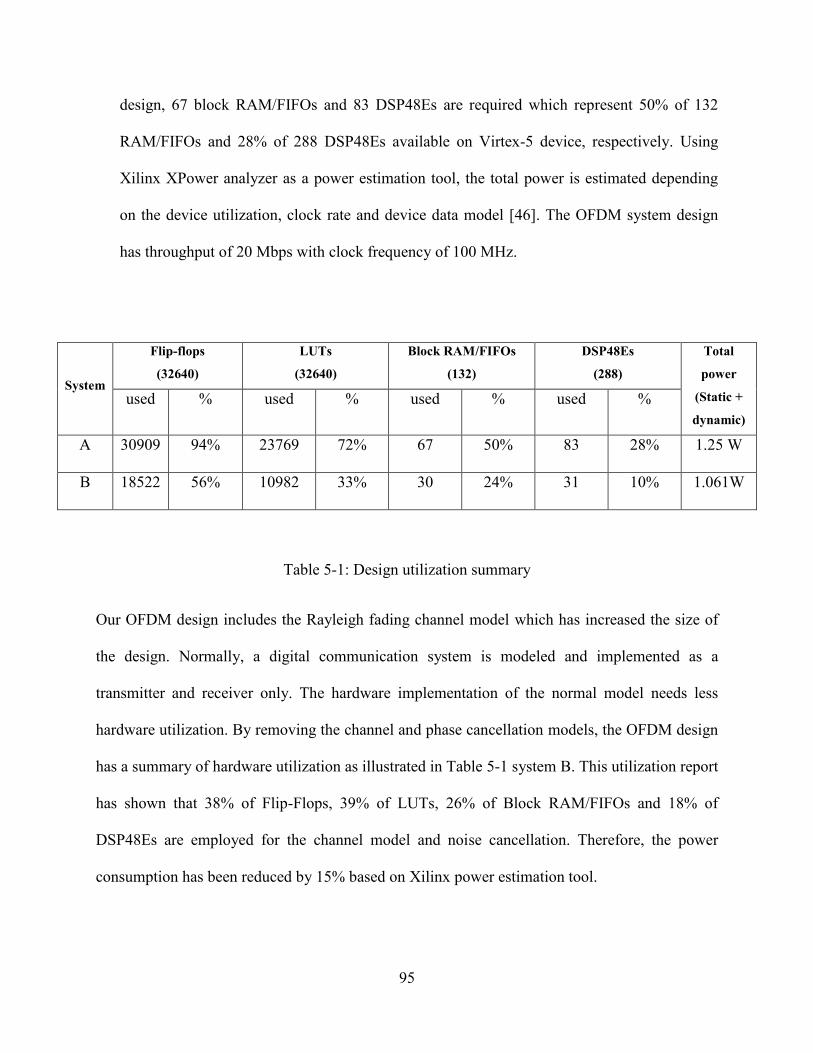
95
design, 67 block RAM/FIFOs and 83 DSP48Es are required which represent 50% of 132
RAM/FIFOs and 28% of 288 DSP48Es available on Virtex-5 device, respectively. Using
Xilinx XPower analyzer as a power estimation tool, the total power is estimated depending
on the device utilization, clock rate and device data model [46]. The OFDM system design
has throughput of 20 Mbps with clock frequency of 100 MHz.
System
Flip-flops
(32640)
LUTs
(32640)
Block RAM/FIFOs
(132)
DSP48Es
(288)
Total
power
(Static +
dynamic)
used % used % used % used %
A 30909 94% 23769 72% 67 50% 83 28% 1.25 W
B 18522 56% 10982 33% 30 24% 31 10% 1.061W
Table 5-1: Design utilization summary
Our OFDM design includes the Rayleigh fading channel model which has increased the size of
the design. Normally, a digital communication system is modeled and implemented as a
transmitter and receiver only. The hardware implementation of the normal model needs less
hardware utilization. By removing the channel and phase cancellation models, the OFDM design
has a summary of hardware utilization as illustrated in Table 5-1 system B. This utilization report
has shown that 38% of Flip-Flops, 39% of LUTs, 26% of Block RAM/FIFOs and 18% of
DSP48Es are employed for the channel model and noise cancellation. Therefore, the power
consumption has been reduced by 15% based on Xilinx power estimation tool.

96
In comparison of our OFDM design results with recent conference paper [14] published
in 2010, we have made a significant improvement in FPGA implementation of OFDM system
and BER performance with fixed-point representation. This conference paper has worked on
FPGA implementation of OFDM transceiver with FFT size of 64. The system was tested over
AWGN channel in Simulink environment. The transmitted OFDM symbols did not include
cyclic prefix. The BER performance with fixed-point representation was worse than the
theoretical curve. Table 5-2 shows the comparison between our OFDM design and the OFDM
design in the conference paper.
Table 5-2: Comparison between our design and work published in 2010
In terms of hardware utilization, our OFDM design has utilized more flip-flops, LUTs and
RAMs due to the implementation of CP insertion and removal, large size of FFT and large
number of bits for fixed-point representation. However, the BER performance of our OFDM
design matches the theoretical curve while the BER performance of the previous work does not.
Also, the number of DSP48 blocks used in our design is less compared with the conference paper
published in 2010.
System design FFT size Adding
CP Channel BER
Fixed –point
representation FPGA
Previous work
in 2010 64 No AWGN in Simulink
Worse than
theoretical curve 16 bits Virtex-4
Our OFDM
Design 512 Yes
Multipath fading
implemented in
hardware
Matching the
theoretical curve 18 bits Virtex-5

97
5.5 Summary
XtremeDSP development kits are designated for FPGA hardware implementation of our
OFDM design due to its advantage of high performance in signal processing. The Xilinx OFDM
design was simulated in Simulink to evaluate the results for hardware implementation. The
results have shown that the OFDM transmitted signal has bandwidth of 12.5 MHz in the range of
-6.25 and +6.25MHz. The hardware co-simulation was overviewed as well as Xtreme DSP
Xilinx Virtex-5 ML506 platform with its specifications and advantages. The co-simulations steps
taken for our design were introduced as a guide of performing JTAG hardware co-simulation on
ML506 platform. The hardware co-simulation results have proven the accurate BER
performance of the Xilinx design despite the use of fixed-point representation. In fact, these
results have been found in conformity with the theoretical observation of OFDM system over
multipath fading channel. A summary of hardware utilizations for the OFDM design
implementation was provided including the power consumption.

98
Chapter 6
Conclusion and Future Work
An OFDM communication system using QPSK modulation scheme was modeled and
implemented on FPGA based on 3GPP LTE standard over multipath fading channel. Our
primary goal was to implement a reliable and efficient design in hardware. To design a circuitry
with the 3GPP LTE specifications, the design flow demonstrated in chapter three was utilized to
fulfill the physical layer requirements. Going through different stages of the design flow, the
system was designed starting with floating-point modeling and ending with fixed-point hardware
implementation.
In the first phase of this research, two OFDM systems with normal and extended CPs
were modeled and simulated in MATLAB based on the OFDM LTE parameters. The main idea
of modeling two different systems was to choose the most robust system to frequency-Selective
fading. To compare the systems’ performance, multi-path fading channel was modeled using the
exponential model, which is suitable for wireless indoor channel. Different multipath channels
were actually applied on both systems in MATLAB to test their resistance to intersymbol
interference. The results have proven that OFDM system with extended CP is more powerful
dealing with frequency-selective fading channel in wideband digital communications. Also it
was determined that the cyclic prefix has to be longer that the extensive delay spread of the
wireless channel in order to avoid intersymbol interference. As the OFDM system extended CP
showed better performance, it was selected for FPGA implementation.

99
A model-based design was built in Simulink for the extended-CP OFDM system. The
Simulink model is a multi-rate system with different sampling rates due to the performance of
up/down sampling and conversion. The modeling and simulation were performed with floating-
point representation to provide the BER curve. The additive white noise channel was applied in
the Simulink model to show the performance of QPSK-OFDM system over AWGN.
The next stage of the design flow actually relied on the Simulink model for modeling
OFDM system using Xilinx System Generator. With high data rate afforded by Xilinx-based
implementation, the system was designed to tranceive a digital signal with bit rate of 20 Mbps
depending on the clock frequency of the target board. Each part of QPSK-OFDM system was
implemented using Xilinx blockset library. Not only AWGN channel was applied using Xilinx
System Generator, but also a Xilinx-based model for multi-path fading channel was proposed as
well. With perfect knowledge of the channel information state, the noise was cancelled in the
receiver side. In Xilinx design, fixed-point representation of 18bits was applied in order to
provide high performance with acceptable area for FPGA implementation. The transmitter,
wireless channel and receiver were implemented on Xilinx Virtex-5. The hardware co-simulation
was performed to verify the design in actual hardware using Virtex-5 ML506 platform. The
hardware co-simulation results showed the high performance of the design.
This work introduced new features of FPGA implementing OFDM system with CP and
multipath fading channel using Xilinx blocks. The system verification was performed through
hardware co-simulation. Also the BER curve of hardware co-simulation was presented to prove
that the Xilinx design has achieved high OFDM performance provided by hardware co-
simulation.

100
This thesis presented a thorough description for Xilinx design of OFDM system and
wireless frequency-selective channel. This work can facilitate the way to many future researches
and projects on OFDM implementation. There is a possibility that Application Specific
Integrated Circuit (ASIC) developers use this thesis as the basis for OFDM implementation on
ASIC rather than FPGA. A few areas were not considered in this work such as synchronization,
carrier recovery, channel coding and estimation. Researchers can use different algorithms to
implement these aspects. Another possibility is to use another digital modulation such as
16QAM, which will increase the bit rate of OFDM design.
Future works can look on finding a solution when the delay spread is more than the
cyclic prefix. There is a chance to designate several subcarriers as pilot subcarriers for phase and
amplitude synchronization at the receiver. The OFDM design can be modified to implement
different IEEE standards such as IEEE 802.16 as well.

101
Bibliography
[1] Adarsh B. Narasimhamurthy, Mahesh K. Banavar, and Cihan Tepedelenlioglu, OFDM
Systems for Wireless Commuincations, Morgan & Claypool Publishers, Mar 10, 2010.
[2] R. V. Nee, OFDM for wireless multimedia Communications, Artech House Publishers, Dec
1999.
[3] R. Chang, "High-speed multichannel data transmission with bandlimited orthogonal
signals," Bell Syst. Tech. Journal, vol. 45, pp. 1775- 1796, Dec. 1966.
[4] "Orthogonal Frequency Division Multiplexing". US Patent 3,488,455, 6 January 1970.
[5] B. Saltzberg, "Performance of an Efficient Parallel Data Transmission System," IEEE
Transaction on Communication, vol. 15, no. 6, p. 805 –811, December 1967.
[6] Peled, A. and Ruiz, A, "Frequency domain data transmission using reduced computational
complexity algorithms," in Acoustics, Speech, and Signal Processing, IEEE International
Conference on ICASSP '80, Apr. 1980.
[7] B. Hirosaki, "An analysis of automatic equalizers for orthogonally multiplexed QAM
systems," IEEE Trans. Commun, Vols. COM-28, pp. 73-83, Jan.1980.
[8] L. Cimini, "Analysis and simulation of a digital mobile channel using orthogonal," IEEE
Trans. Commun, Vols. COM-33, pp. 665-675, July 1985.
[9] F. Manavi and Y. R. Shayan, "Implementation of OFDM modem for the Physical Layer of
IEEE 802.11a Standard Based on Xilinx Virtex-II FPGA," in IEEE 59th Vehicular
Technology Conference (VTC 2004-Spring), Milan, Italy, May 17-19, 2004.

102
[10] X. Jinsong, L. Xiaochun, W. Haitao, B. Yujing, Z. Decai, Z. Xiaolong, W. Chaogang,
"Implementation of MB-OFDM Transmitter Baseband Based on FPGA," in 4th IEEE
International Conference on Circuits and Systems for Communications (ICCSC 2008), May
2008.
[11] M. Santhi, M.S. Kumar, G. Lakshminarayanan, T.N. Prabakar, "Design and implementation
of pipelined MBOFDM UWB transmitter backend modules on FPGA," in International
Conference on Computing, Communication and Networking, (ICCCn 2008), 18-20 Dec.
2008.
[12] Ahmad Sghaier, Shawki Areibi and Bob Dony, "A PIPELINED IMPLEMENTATION OF
OFDM TRANSMISSION ON RECONFIGURABLE PLATFORMS," in Canadian
Conference on Electrical and Computer Engineering, (CCECE 2008), 2008.
[13] Joaquin Garcia, Rene Cumplido, "On the design of an FPGA-Based OFDM modulator for
IEEE 802.11a," in 2nd International Conference on Electrical and Electronics Engineering
(ICEEE), September 2005.
[14] K. Sobaihi, A. Hammoudeh, D. Scammell, "FPGA Implementation of OFDM Transceiver
for a 60GHz Wireless Mobile Radio System”," in 2010 International Conference On
Reconfigrable Computing, 2010.
[15] Shaminder Kaur, Rajesh Mehra, "FPGA Implementation of OFDM Transceiver using FFT
Algorithm," International Journal of Engineering Science and Technology (IJEST), vol. 4,
Apr 2012.
[16] V. Tarokh, New Directions in Wireless Communications Research, Springer, 2009.
[17] Shinsuke Hara and Ramjee Prasad, Multicarrier Techniques for 4G Mobile

103
Communications, Artech House, June, 2003.
[18] R. Prasad, OFDM for Wireless Communications Systems, Artech House Publishers, 2004.
[19] T. S. Rappaport, Wireless Communications: Principles and Practice, Prentice Hall, 2002.
[20] Ye Geoffrey Li, Gordon L. Stuber, Orthogonal Frequency Division Multiplexing for
Wireless Communications, Springer, 2006.
[21] T.-D. Chiueh, OFDM baseband receiver Design for wireless communincations, Wiley, Nov
2007.
[22] Yong Soo Cho, Jaekwon Kim , Won Young Yang, Chung G. Kang, MIMO-OFDM
Wireless Communications with MATLAB, Wiley-IEEE Press, 2010.
[23] A. Goldsmith, Wireless Communications, Cambridge University Press, 2005.
[24] Michel C. Jeruchim, Philip Balaban and K. Sam Shanmugan, Simulation of Communication
Systems: Modeling, Methodology and Techniques, Springer; 2nd edition, October 31, 2000.
[25] A. F. Molisch, Wireless Communications, Wiley; 2 edition , December 7, 2010.
[26] Arunabha Ghosh, Jun Zhang, Jeffrey G. Andrews and Rias Muhamed, Fundamentals of
LTE, Prentice Hall, September 2010.
[27] Stefania Sesia, Issam Toufik and Matthew Baker, LTE, The UMTS Long Term Evolution:
From Theory to Practice, Wiley, 2009.
[28] B. Furht, Long Term Evolution: 3GPP LTE Radio and Cellular Technology, Auerbach
Publications , April 23, 2009.
[29] B. Skla, Digital Communications: Fundamentals and Applications, 2nd ed., Prentice Hall,
2002.

104
[30] Cooley, J. W., Tukey, J. W., "An Algorithm for the Machine Computation of the Complex
Fourier Series," Mathematics of Computation, vol. 19, pp. 297-301, April 1965.
[31] P. a. M. V. Duhamel, "Fast Fourier Transforms: A Tutorial Review and a State of the Art,"
Signal Processing, vol. 19, pp. 259-299, April 1990.
[32] Oppenheim, A. V., Schafer, R. W., Discrete-time signal processing, Prentice Hall, 1989.
[33] "Mathworks," [Online]. Available: http://www.mathworks.com.
[34] "Xilinx System Generator for DSP Getting Started Guide Release 9.2.01," Xilinx Inc.,
October 2007.
[35] "Xilinx System Generator for DSP Getting Reference Guide Release 10.1," Xilinx Inc.,
March 2008.
[36] P. Dong, "Design and FPGA Implementation of a SISO and a MIMO Wireless System for
Software Defined Radio," Thesis, Spring 2009.
[37] "Xilinx DS260 LogicCORE IP Fast Fourier Transform v7.1 Data sheet," Xilinx Inc., 2011.
[38] A. Ghazel, E. Boutillon, J. L. Danger, G. Gulak and H. Laamari, "Design and Performance
Analysis of a High Speed AWGN Communication Channel Emulator," in IEEE PACRIM
Conference, Victoria, BC, August 2001.
[39] J. Volder, "The CORDIC trigonometric computing technique," IRE Transactions on
Electronic Computers, vol. 3, p. 330–334, 1959.
[40] J. Ou, "MATLAB/Simulink Based Hardware/Software Co-Simulation for Designing Using
FPGA Configured Soft Processors," in 19th IEEE International Parallel and Distributed
Processing Symposium (IPDPS’05), 2005.
[41] "ML505/ML506/ML507 Evaluation Platform User Guide," Xilinx Inc., May16, 2011.

105
[42] "ML505/ML506/ML507 Reference Design User Guide," Xilinx inc., June 23, 2009.
[43] "ML505/506/507 Overview and Setup," Xilinx Inc., May 2009.
[44] "System Generator For DSP User Guide," Xilinx Inc, October 19, 2011.
[45] "Virtex-5 Family Overview," Xilinx Inc., February 6, 2009.
[46] "XPower Estimator User Guide," Xilinx Inc., January 18, 2012.