16. a VHDL Implementation of UART Design With BIST Capability
International Research Journal of Engineering and Technology (IRJET) e-ISSN: 2395 -0056
Volume: 03 Issue: 02 | Feb-2016 www.irjet.net p-ISSN: 2395-0072
© 2016, IRJET | Impact Factor value: 4.45 | ISO 9001:2008 Certified Journal | Page 1231
FPGA IMPLEMENTATION OF BIST IN OFDM TRANSCEIVERS
Rinitha.R1, Ponni.R2
1PG student, Dept. of Electronics and Communication Engineering, Kings College of Engineering, Tamilnadu, India
2Assistant Professor, Dept. of Electronics and Communication Engineering, Kings College of Engineering, Tamilnadu, India
---------------------------------------------------------------------***---------------------------------------------------------------------Abstract - Testing of VLSI circuits is an essential one to ensure the high quality and proper functionality of the system. Due to the circuit complexity, it is very difficult to test it. For this issue the concept of Built-in Self-Test (BIST) is introduced. BIST is a mechanism that permits a circuit to test itself. Small additional circuitry, power or envelope detectors can be used for BIST purpose. BIST in wireless communication system measure the imbalance parameters and non linear characteristics. Here the BIST is used in Orthogonal Frequency Division Multiplexing (OFDM) transceivers for the detection of Bit Error Rate (BER) and also reduce it. BER can be demarcated as the number of received bits of a data stream over a communication channel that can be affected due to noise, interference and distortion or bit synchronization errors. This system mainly focuses the performance of OFDM –PSK, BPSK and QPSK system by using Reed-Solomon codes. These codes are used to encode the data stream that can be passed through communication channels resembling AWGN (Additive White Gaussian Noise) channel. Various simulations are performed for different modulation schemes in MATLAB to find best BER performance. Key Words: Built-in Self-Test (BIST), Orthogonal Frequency Division Multiplexing (OFDM), Bit Error Rate (BER), Additive White Gaussian Noise(AWGN), Reed-Solomon codes.
1.INTRODUCTION Test cost becomes a significant contributor to the production cost. Efforts to reduce the manufacturing cost require the need of BIST implementation in contrast to Automatic Test Equipment (ATE) which results in higher capital and operational cost. It helps reduction of test time as it reduces the switching time of ATE instruments and measurement of complex circuitry using low cost testing solutions. In most Built-in-Self-Test (BIST) techniques, a small piece of circuit is added to the design in order to convert the system response to a simpler form with lower frequency that makes on-chip analysis feasible. The Radio Frequency (RF) to low frequency conversion in BIST can be enabled using peak, power, or envelope detectors.
Such BIST techniques have been proposed to characterize RF blocks, such as low noise amplifiers (LNAs), or power amplifiers (PAs), or the entire transmitter chain. The BIST circuit detects amplitude alterations at the outputs of the differential LNA due to parametric or catastrophic faults, and
provides a single digital Pass/Fail indication signal. Most of the prior work on BIST for transceivers focuses on the characterization of noise figure, gain and nonlinearity of the devices. However, the Bit Error Rate (BER) is also detrimental and need to be characterized. So the BIST circuit is used in Orthogonal Frequency Division Multiplexing (OFDM) system for the measure of BER. In wireless communication the system performance is determined by the BER performance. It is increasingly believed that OFDM results in an improved downlink multimedia service require high data rate communications, but this condition is significantly limited by inter-symbol interference (ISI) due to the existence of the multiple paths. There are many multicarrier modulation techniques.
During digital data transmission and storage operations, performance criterion is commonly determined by BER. It is the ratio of the number of error bits to the number of total bits. Noise in transmission medium disrupts the signal and causes data corruptions. Relation between signal and noise power is described with SNR (Signal-to-Noise Ratio). Generally, SNR is explained with signal power/BER. It means, the less the BER result is the higher the SNR and the better communication quality. To meet the requirements discussed above, BIST circuit is used in OFDM based wireless communication system.
2. CONCEPT OF BIST IN TRANSCEIVERS The increasing functional complexity of electronic components and system makes testing a demanding task, particularly under the constraints of high quality and low cost. The different test approaches have been developed to describe the circuit at different levels based on the existing variety of models. They are Functional testing, IDDQ test, Scan test etc. But compare to other testing methods BIST is more efficient and also consist of many advantages over testing. The basic architecture of BIST is shown in Figure 1 which consist of Input, CUT and Output
Fig-1: Basic BIST architecture
The above BIST architecture consist of three steps: The
International Research Journal of Engineering and Technology (IRJET) e-ISSN: 2395 -0056
Volume: 03 Issue: 02 | Feb-2016 www.irjet.net p-ISSN: 2395-0072
© 2016, IRJET | Impact Factor value: 4.45 | ISO 9001:2008 Certified Journal | Page 1232
first step is defined as initial state or it uses some functionality by applying the input response to the circuit. In the second step the circuit processes the input response. The third step is checking and produces the correct output response of the circuit. Generally the BIST circuit is used in transceiver for the measurement of non-linear parameters like phase noise, noise margin, Signal to Noise Ratio (SNR), in-phase and quadrature imbalance. The BIST circuit with Reed Solomon (RS) coder blocks in the transceivers for the measure of BER.
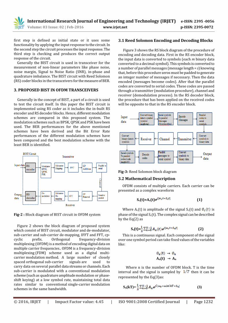
3. PROPOSED BIST IN OFDM TRANSCEIVERS Generally in the concept of BIST, a part of a circuit is used to test the circuit itself. In this paper the BIST circuit is implemented using RS coder as it includes the in-built RS encoder and RS decoder blocks. Hence, different modulation schemes are compared in this proposed system. The modulation schemes such as BPSK, QPSK and PSK have been used. The BER performances for the above mentioned schemes have been derived and the Bit Error Rate performances of the different modulation schemes have been compared and the best modulation scheme with the least BER is identified.
Fig-2 : Block diagram of BIST circuit in OFDM system
Figure 2 shows the block diagram of proposed system which consist of BIST circuit, modulator and de-modulator, sub-carrier and sub-carrier de-mapping, IFFT and FFT, cp-cyclic prefix. Orthogonal frequency-division multiplexing (OFDM) is a method of encoding digital data on multiple carrier frequencies.. OFDM is a frequency-division multiplexing (FDM) scheme used as a digital multi- carrier modulation method. A large number of closely spaced orthogonal sub-carrier signals are used to carry data on several parallel data streams or channels. Each sub-carrier is modulated with a conventional modulation scheme (such as quadrature amplitude modulation or phase-shift keying) at a low symbol rate, maintaining total data rates similar to conventional single-carrier modulation schemes in the same bandwidth.
3.1 Reed Solomon Encoding and Decoding Blocks Figure 3 shows the RS block diagram of the procedure of encoding and decoding data. First in the RS encoder block, the input data is converted to symbols (each m binary data converted to a decimal symbol). This symbols is converted to a number of parallel messages (message length = s) knowing that, before this procedure zeros must be padded to generate an integer number of messages if necessary. Then the data encoded (messages become codes). After that the parallel codes are converted to serial codes. These codes are passed through a transmitter (modulation procedure), channel and receiver (demodulation process). In the RS decoder block, the procedure that has been applied on the received codes will be opposite to that in the RS encoder block.
Fig-3: Reed Solomon block diagram
3.2 Mathematical Description
OFDM consists of multiple carriers. Each carrier can be presented as a complex waveform
Sc(t)=Ac(t) (1)
Where Ac(t) is amplitude of the signal Sc(t) and is
phase of the signal Sc(t). The complex signal can be described by the Eq(2) as
Ss(t)= (2)
This is a continuous signal. Each component of the signal over one symbol period can take fixed values of the variables like:
→
An(t) → An
Where n is the number of OFDM block. T is the time interval and the signal is sampled by then it can be
represented by the Eq(3)as:
SS(kT)= (3)
International Research Journal of Engineering and Technology (IRJET) e-ISSN: 2395 -0056
Volume: 03 Issue: 02 | Feb-2016 www.irjet.net p-ISSN: 2395-0072
© 2016, IRJET | Impact Factor value: 4.45 | ISO 9001:2008 Certified Journal | Page 1233
Let then the signal becomes :
SS(kT) = (4)
The signal is compared with general Inverse Fourier Transform (IFT):
g(kT) = (5)
Here, s(kT) is time domain signal .
Here, is symbol duration period. The OFDM signal can
be defined by Fourier Transform. The use of Fast Fourier Transform (FFT) can obtain frequency domain OFDM symbols and Inverse Fast Fourier Transform (IFFT) can obtain time domain symbols. These can be written as: Fast Fourier Transform
(6)
Inverse Fast Fourier Transform
(7)
Where, 0
BER Calculation:
The BER of BPSK in AWGN can be calculated as:
or
Since there is only one bit per symbol, this is also the symbol error rate.
For M-PSK
(8)
For QPSK
(9)
The symbol error rate is given by:
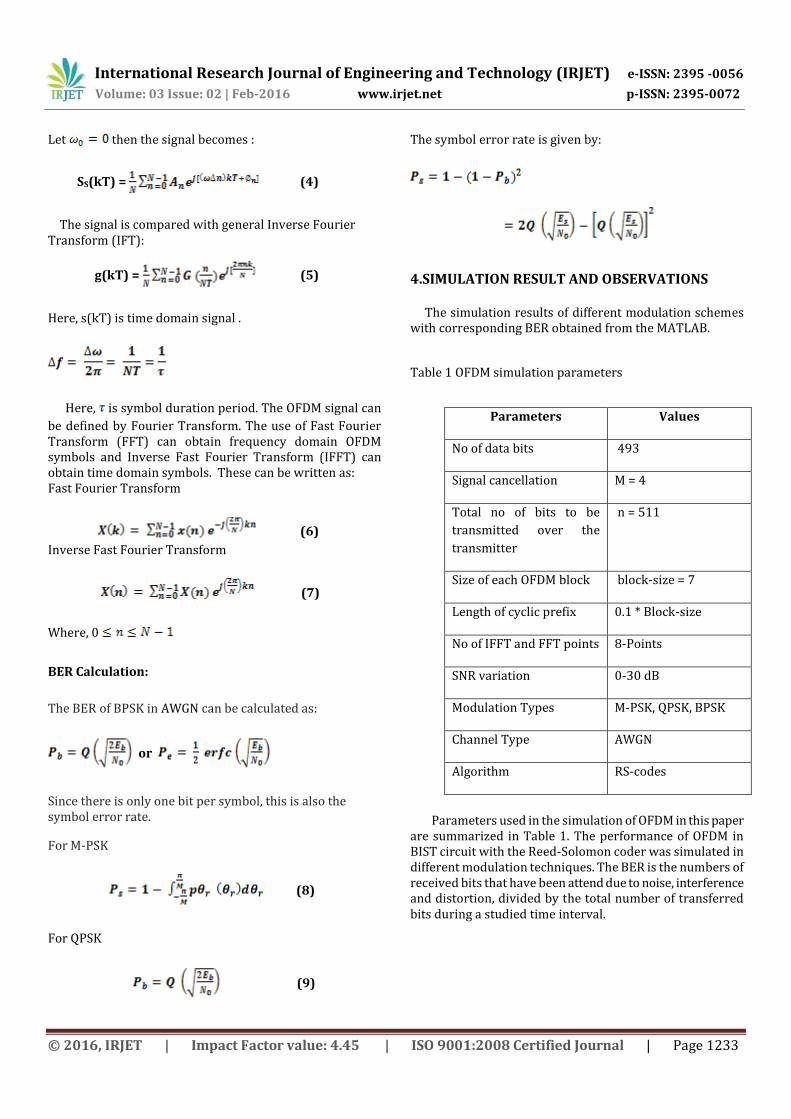
4.SIMULATION RESULT AND OBSERVATIONS The simulation results of different modulation schemes with corresponding BER obtained from the MATLAB.
Table 1 OFDM simulation parameters
Parameters used in the simulation of OFDM in this paper are summarized in Table 1. The performance of OFDM in BIST circuit with the Reed-Solomon coder was simulated in different modulation techniques. The BER is the numbers of received bits that have been attend due to noise, interference and distortion, divided by the total number of transferred bits during a studied time interval.
Parameters Values
No of data bits 493
Signal cancellation M = 4
Total no of bits to be
transmitted over the
transmitter
n = 511
Size of each OFDM block block-size = 7
Length of cyclic prefix 0.1 * Block-size
No of IFFT and FFT points 8-Points
SNR variation 0-30 dB
Modulation Types M-PSK, QPSK, BPSK
Channel Type AWGN
Algorithm RS-codes
International Research Journal of Engineering and Technology (IRJET) e-ISSN: 2395 -0056
Volume: 03 Issue: 02 | Feb-2016 www.irjet.net p-ISSN: 2395-0072
© 2016, IRJET | Impact Factor value: 4.45 | ISO 9001:2008 Certified Journal | Page 1234
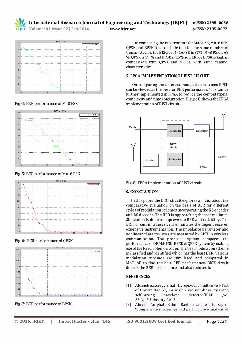
Fig-4: BER performance of M=8 PSK
Fig-5: BER performance of M=16 PSK
Fig-6: BER performance of QPSK
Fig-7: BER performance of BPSK
On comparing the Bit error rate for M=8 PSK, M=16 PSK, QPSK and BPSK it is conclude that for the same number of transmitted bit the BER for M=16PSK is 83%, M=8 PSK is 68 %, QPSK is 39 % and BPSK is 15% so BER for BPSK is high in comparison with QPSK and M-PSK with same channel characteristics.
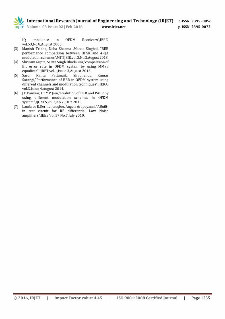
5. FPGA IMPLEMENTATION OF BIST CIRCUIT
On comparing the different modulation schemes BPSK can be viewed as the best for BER performance. This can be further implemented in FPGA to reduce the computational complexity and time consumption. Figure 8 shows the FPGA implementation of BIST circuit.
Fig-8: FPGA implementation of BIST circuit
6. CONCLUSION
In this paper the BIST circuit explores an idea about the comparative evaluation on the basis of BER for different styles of modulation schemes incorporating the RS encoder and RS decoder. The BER is approaching theoretical limits. Simulation is done to improve the BER and reliability. The BIST circuit in transceivers eliminates the dependence on expensive instrumentation. The imbalance parameter and nonlinear characteristics are measured by BIST in wireless communication. The proposed system compares the performance of OFDM-PSK, BPSK & QPSK system by making use of the Reed Solomon coder. The best modulation scheme is classified and identified which has the least BER. Various modulation schemes are simulated and compared in MATLAB to find the best BER performance. BIST circuit detects the BER performance and also reduces it.
REFERENCES
[1] Afsaneh nassery , sirnath byregowda ,”Built-in Self-Test of transmitter I/Q mismatch and non-linearity using self-mixing envelope detector”IEEE ,vol 23,No.2,February 2015.
[2] Alireza Tarighat, Rahim Bagheri and Ali H. Sayed, “compensation schemes and performance analysis of
International Research Journal of Engineering and Technology (IRJET) e-ISSN: 2395 -0056
Volume: 03 Issue: 02 | Feb-2016 www.irjet.net p-ISSN: 2395-0072
© 2016, IRJET | Impact Factor value: 4.45 | ISO 9001:2008 Certified Journal | Page 1235
IQ imbalance in OFDM Receivers”,IEEE, vol.53,No.8,August 2005.
[3] Manish Trikha, Neha Sharma ,Manas Singhal, “BER performance comparison between QPSK and 4-QA modulation schemes”,MITIJEIE,vol.3,No.2,August 2013.
[4] Shriram Gupta, Sarita Singh Bhadauria,”comparision of Bit error rate in OFDM system by using MMSE equalizer”,IJRET,vol.1,Issue 3,August 2013.
[5] Saroj Kanta Pattanaik, Shubhendu Kumar Sarangi,”Performance of BER in OFDM system using different channels and modulation techniques”,IJERA, vol.3,Issue 4,August 2014.
[6] J.P.Panwar, Dr.Y.V.Jain,”Evalution of BER and PAPR by using different modulation schemes in OFDM system”,IJCNCS,vol.3,No.7,JULY 2015.
[7] Lambros E.Dermentzoglou, Angela Arapoyanni,”ABuilt-in test circuit for RF differential Low Noise amplifiers”,IEEE,Vol.57,No.7,July 2010.