Design and Development of 8-Bits Fast Multiplier for Low ...ijetch.org/papers/482-C094.pdf ·...
7
Abstract—High speed multiplication has always been a fundamental requirement of high performance processors and systems. With MOS scaling and technological advances there is a need for design and development of high speed data path operators such as adders and multipliers to perform signal processing operations at very high speed supporting higher data rates. In DSP applications, multiplication is one of the most utilized arithmetic operations as part of filters, convolves and transforms processors. Improving multipliers design directly benefits the high performance embedded processors used in consumer and industrial electronic products. Hence there is a need for design and development of high-speed architectures for N-bit multipliers supporting high speed and power. Here we review the architecture reported in the literature for multipliers and critical issues degrading the speed and power of these multiplier. Based on this review suitable modifications are suggested in the design for high speed and low power multipliers. Index Terms— CPA, DSP, microprocessor, multiplier. I. INTRODUCTION Multiplication is a less common operation than addition, but is still essential for microprocessors, digital signal processors and graphics engines. Multiplication algorithms are used to illustrate methods of designing different cells so that they fit into a large structure. The most basic form of multiplication consists of forming the product of two unsigned binary numbers, simplified to base 2. M × N bits multiplication can be viewed as forming N partial products of M bits each, and then summing the appropriately shifted partial products to produce on M + N bits result P[1]. Binary multiplication is equivalent to a logical AND operation. Therefore, generating partial product consists of logical ANDing of the appropriate bits of the multiplier and multiplicand. Each column of partial products must then be added and if necessary, any carry values passed to the next columns. A. Parallel Multipliers In the 1960's two classes of parallel multipliers were defined. The first class [1] of parallel multipliers uses a rectangular array of identical combinational cells to generate and sum the partial product bits. Multipliers of this type are called array multipliers. They have a delay that is generally Manuscript received June 20, 2012; revised July 30, 2012. Vasudev G. is with the ACS College of Engineering, Bangalore, India- 560 032 (e-mail:[email protected]). Rajendra Hegadi is with the Pragati College of Engineering and Management, Raipur (C.G)-492015, India (e-mail: [email protected]). proportional to the word length of the multiplier input. Due to the regularity of their structures, array multipliers are carrying to layout and have been implemented frequently. The second class of parallel multipliers reduces a matrix of partial product bits to two words through the strategic application of counters or compressors [2]. These two words are then summed using a fast carry-propagate adder to generate the product. This class of parallel multiplier is known as column compression multiplier. These are also fastest multiplier as the delay is proportional to the logarithm of the multiplier and word length. B. Array Multipliers In array multiplier the two basic functions, partial product generation and summations are combined. For unsigned N × N multiplication, N 2 +N-1 cells (where N 2 contain an AND gate for partial product generation, a full adder for summing and N-1 cells containing a full adder) are connected to produce a multiplier. This array generates N lower product bits directly and uses a carry-propagate adder, in this case a ripple carry adder, to form the upper N bits of the product. C. Column Compression Multiplier Column compression multiplier continued to be studied due to their high speed performance. This multiplier’s total delay is proportional to the logarithm of the operand word length. These multipliers are faster than array multipliers whose delay grows linearly with operand word length. According to Thomas Ko Callaway et. al. [3] column compression multipliers are more power efficient than array multipliers. In 1964, Wallace [4] introduced a scheme for fast multiplication based on summing the partial product bits on parallel using a tree of carry save adders which became generally known as the Wallace tree. Dadda [5] later refined Wallace's method by defining a counter placement strategy that required fewer counters in the partial product reduction stage at the cost of a larger carry-propagate adder. For both methods, the total delay is proportional to the logarithm of the operand word-length. Other partial product reduction methods have been proposed since the work of Wallace and Dadda. The reduced area [6] and the Windsor methods are based on strategic utilization of (3, 2) and (2, 2) counters to improve area and layout, while maintaining the fast speed of the Wallace and Dadda designs. In this paper we identify techniques for optimal computer aided designs of column compression multipliers by analyzing area, power and timing characteristics with particular emphasis on low power. Design and Development of 8-Bits Fast Multiplier for Low Power Applications Vasudev G. and Rajendra Hegadi, Member, IACSIT IACSIT International Journal of Engineering and Technology, Vol. 4, No. 6, December 2012 774 DOI: 10.7763/IJET.2012.V4.482
Transcript of Design and Development of 8-Bits Fast Multiplier for Low ...ijetch.org/papers/482-C094.pdf ·...

Abstract—High speed multiplication has always been a
fundamental requirement of high performance processors and systems. With MOS scaling and technological advances there is a need for design and development of high speed data path operators such as adders and multipliers to perform signal processing operations at very high speed supporting higher data rates. In DSP applications, multiplication is one of the most utilized arithmetic operations as part of filters, convolves and transforms processors. Improving multipliers design directly benefits the high performance embedded processors used in consumer and industrial electronic products. Hence there is a need for design and development of high-speed architectures for N-bit multipliers supporting high speed and power. Here we review the architecture reported in the literature for multipliers and critical issues degrading the speed and power of these multiplier. Based on this review suitable modifications are suggested in the design for high speed and low power multipliers.
Index Terms— CPA, DSP, microprocessor, multiplier.
I. INTRODUCTION Multiplication is a less common operation than addition,
but is still essential for microprocessors, digital signal processors and graphics engines. Multiplication algorithms are used to illustrate methods of designing different cells so that they fit into a large structure. The most basic form of multiplication consists of forming the product of two unsigned binary numbers, simplified to base 2.
M × N bits multiplication can be viewed as forming N partial products of M bits each, and then summing the appropriately shifted partial products to produce on M + N bits result P[1]. Binary multiplication is equivalent to a logical AND operation. Therefore, generating partial product consists of logical ANDing of the appropriate bits of the multiplier and multiplicand. Each column of partial products must then be added and if necessary, any carry values passed to the next columns.
A. Parallel Multipliers In the 1960's two classes of parallel multipliers were
defined. The first class [1] of parallel multipliers uses a rectangular array of identical combinational cells to generate and sum the partial product bits. Multipliers of this type are called array multipliers. They have a delay that is generally
Manuscript received June 20, 2012; revised July 30, 2012. Vasudev G. is with the ACS College of Engineering, Bangalore, India-
560 032 (e-mail:[email protected]). Rajendra Hegadi is with the Pragati College of Engineering and
Management, Raipur (C.G)-492015, India (e-mail: [email protected]).
proportional to the word length of the multiplier input. Due to the regularity of their structures, array multipliers are carrying to layout and have been implemented frequently.
The second class of parallel multipliers reduces a matrix of partial product bits to two words through the strategic application of counters or compressors [2]. These two words are then summed using a fast carry-propagate adder to generate the product. This class of parallel multiplier is known as column compression multiplier. These are also fastest multiplier as the delay is proportional to the logarithm of the multiplier and word length.
B. Array Multipliers In array multiplier the two basic functions, partial product
generation and summations are combined. For unsigned N × N multiplication, N2+N-1 cells (where N2 contain an AND gate for partial product generation, a full adder for summing and N-1 cells containing a full adder) are connected to produce a multiplier. This array generates N lower product bits directly and uses a carry-propagate adder, in this case a ripple carry adder, to form the upper N bits of the product.
C. Column Compression Multiplier Column compression multiplier continued to be studied
due to their high speed performance. This multiplier’s total delay is proportional to the logarithm of the operand word length. These multipliers are faster than array multipliers whose delay grows linearly with operand word length. According to Thomas Ko Callaway et. al. [3] column compression multipliers are more power efficient than array multipliers. In 1964, Wallace [4] introduced a scheme for fast multiplication based on summing the partial product bits on parallel using a tree of carry save adders which became generally known as the Wallace tree. Dadda [5] later refined Wallace's method by defining a counter placement strategy that required fewer counters in the partial product reduction stage at the cost of a larger carry-propagate adder. For both methods, the total delay is proportional to the logarithm of the operand word-length. Other partial product reduction methods have been proposed since the work of Wallace and Dadda. The reduced area [6] and the Windsor methods are based on strategic utilization of (3, 2) and (2, 2) counters to improve area and layout, while maintaining the fast speed of the Wallace and Dadda designs.
In this paper we identify techniques for optimal computer aided designs of column compression multipliers by analyzing area, power and timing characteristics with particular emphasis on low power.
Design and Development of 8-Bits Fast Multiplier for Low Power Applications
Vasudev G. and Rajendra Hegadi, Member, IACSIT
IACSIT International Journal of Engineering and Technology, Vol. 4, No. 6, December 2012
774DOI: 10.7763/IJET.2012.V4.482

II. DESIGN AND ANALYSIS The major works in this paper are study of multiplier
architectures for high speed signal processing applications, identifying the specifications for the multiplier design, modeling the architecture, functional verification, and developing the test bench to verify the design for all possible input combinations. We also do FPGA implementation of the proposed multiplier to meet the specification identified. Synopsys tool flow is used for ASIC synthesis, physical design and implementation of multipliers. GDSII generated and report prepared.
Following are the technical specification of experimental work carried out to design and implement Booth, Wallace, Dadda multipliers using 130nm technology. Input bit width: 8-bit, signed, unsigned, integer, decimal. Input arrival: parallel with 100 Mbytes / sec.
Expected output: 16-bit output, supporting all formats. Output data rate: 100 Mbytes /sec. Tech: 130 nm, Lib: TSMC. Power: 10≤ μ watts. Area: 400 sq. mm. The power analysis is the process of calculating the power
consumption of the chip. It also consists of the calculation of voltage, current drop (IR drop) and electromigration analysis due to high current density of the metal. Table I gives the power consumption of the multipliers.
Dadda multiplier consumes less area as compared to that of Wallace tree and Booth Multiplier. Booth multiplier consumes less power as compared to that of Wallace tree and Dadda multiplier. Wallace tree has less delay as compared to that of Booth and Dadda multipliers.
Booth multiplier has maximum number of ROMs, macros and BELS. Wallace tree has minimum number of BELS and macros compared to Booth and Dadda multiplier. Also Wallace tree multiplier and Dadda multiplier have no flip-flops and Booth multiplier has maximum flip-flops.
The multipliers have been synthesized setting a constraint on speed to a maximum of 130MHz. Based on this constraint the table II gives the design compiler output for various factors of the multipliers.
TABLE I: COMPARIAION OF MU LTIPLIERS
8 bit Booth Multiplier
Wallace tree
Dadda Multiplier
Area (μm) 5115.963379 1330.7615 1330.761597
Power(μw) 324.5302 655.5517 655.8073
Timings (ns) 3.75 1.56 1.56
For the multiplication of two numbers y and x, we denote the multiplicand as in (1)
0121 ,...,( yyyyy MM −−= ) (1)
and multiplier as in (2)
0121 ,...,( xxxxx NN −−= ) (2)
For unsigned multiplication, the product is given in (3).
2221
0
1
0
1
0
1
0))(( ji
j
N
i
M
ji
iN
ii
jM
jj yxxyP +
−
=
−
=
−
=
−
=∑∑∑∑ ==
(3)
Number of techniques can be used to perform multiplication. In general, the choice is based up on factors such as latency, throughput, area, and design complexity. An obvious approach is to use an M+1 bits carry propagate adder (CPA) to add the first two partial products, then another CPA to add the third partial product to the running sum, and so forth. Such an approach requires N-1 CPAs and is slow, even if a fast CPA is employed. More efficient parallel approaches use some sort of array or tree of full adders to sum the partial products.
In the early 1950’s, multiplier performance was significantly improved with the introduction of Booth multiplier [7], development of faster adders [8] and memory components.
Booth's method and the modified Booth's method do not require a correction of the product when either (or both) of the operands is (are) negative for two's complement numbers. During the 1950's adder designs moved away from the slow sequential circuit executed by ripple carry adders carry look ahead, carry select, and conditional sum adders yielded speedy sums through the faster simultaneous or parallel generation of carriers.
TABLE II: DESIGN COMPILER OUTPUT
8 bit Multiplier
Booth Wallace tree Dadda
Frequency 130MHZ 130MHZ 130MHZ Number of Ports 38 34 32
Number of Nets 265 302 348
Number of Cells 214 248 266
References 35 5 5
Combinational Area (μm) 1868.8373 1470.7612 1330.7615
Sequential Area (μm) 3247.1262 0.0000 0.0000
Total Cell Area (μm) 5115.9633 1470.7672 1330.7615
Cell internal Power (μw) 303.1691 501.8940 562.0927
Net Switching power μw) 21.3691 153.6577 153.7151 Total Dynamic Power(μw) 324.5302 655.5517 655.8073
Cell Leakage Power (μw) 5.6910 5.6263 5.6258
III. ARRAY MULTIPLIER The two basic functions of array multiplier, partial product
generation and summation are combined. For unsigned N x N multiplication, N2+N-1 cells are connected to produce a multiplier, where N2 contain an AND gate for partial product generation, a full adder for summing and N-1 cells containing a full adder [9]. The array generates N lower product bits directly and uses a carry-propagate adder, in this case a ripple carry adder, to form the upper N bits of the product.
Replacing full adder with half adders, possibly reduces the complexity to N2 AND gates, N half adders, and N(N-2) full adders. The worst case delay is (2N-2) cΔ , where cΔ is the adder delay.
In order to design an array multiplier for two's complement operands, Booth algorithm [10] can be employed. This
IACSIT International Journal of Engineering and Technology, Vol. 4, No. 6, December 2012
775
algorithm computes the partial products by examining two multiplicand bits at a time. Except for enabling usage of two's complement operands, this algorithm offers no performance or area advantage in comparison to the basic array multiplier. Better delays, though can be achieved by implementing a higher radix modified Booth algorithm [11].
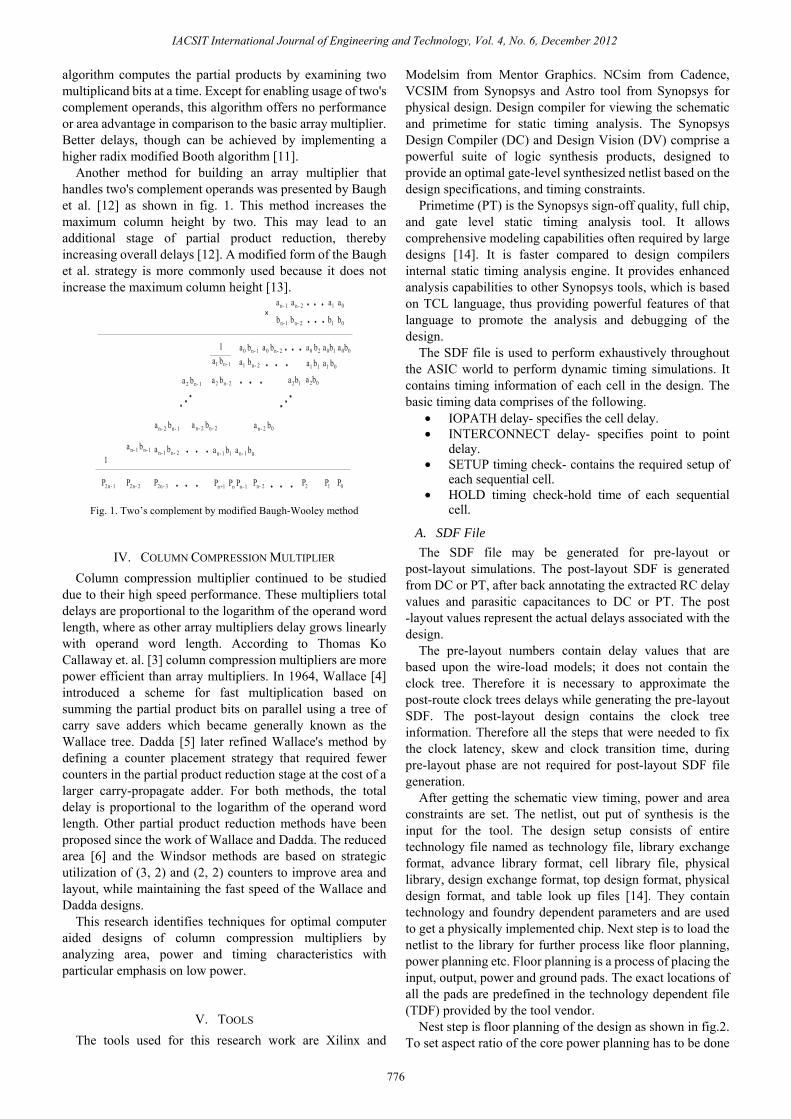
Another method for building an array multiplier that handles two's complement operands was presented by Baugh et al. [12] as shown in fig. 1. This method increases the maximum column height by two. This may lead to an additional stage of partial product reduction, thereby increasing overall delays [12]. A modified form of the Baugh et al. strategy is more commonly used because it does not increase the maximum column height [13].
0 n 1 0 n 2 0 2 0 1 0 0a b a b a b a b a b- -
n 1 n 2 1 0
n 1 n 2 1 0
a a a a
b b b b. . .- -
- -
1 n 1a b -
1
1 n 2a b - 1 1 1 0a b a b
2 n 1a b - 2 n 2a b - 2 1a b 2 0a b
n 2 n 1a b- - n 2 n 2a b- - n 2 0a b-
n 1 n 1a b- - n 1 n 2a b- - n 1 1 n 1 0a b a b- -1
2n 1P - 2n 2P - 2n 3P - n 1P + nP n 1P - n 2P - 2P 1P 0P
×
Fig. 1. Two’s complement by modified Baugh-Wooley method
IV. COLUMN COMPRESSION MULTIPLIER Column compression multiplier continued to be studied
due to their high speed performance. These multipliers total delays are proportional to the logarithm of the operand word length, where as other array multipliers delay grows linearly with operand word length. According to Thomas Ko Callaway et. al. [3] column compression multipliers are more power efficient than array multipliers. In 1964, Wallace [4] introduced a scheme for fast multiplication based on summing the partial product bits on parallel using a tree of carry save adders which became generally known as the Wallace tree. Dadda [5] later refined Wallace's method by defining a counter placement strategy that required fewer counters in the partial product reduction stage at the cost of a larger carry-propagate adder. For both methods, the total delay is proportional to the logarithm of the operand word length. Other partial product reduction methods have been proposed since the work of Wallace and Dadda. The reduced area [6] and the Windsor methods are based on strategic utilization of (3, 2) and (2, 2) counters to improve area and layout, while maintaining the fast speed of the Wallace and Dadda designs.
This research identifies techniques for optimal computer aided designs of column compression multipliers by analyzing area, power and timing characteristics with particular emphasis on low power.
V. TOOLS The tools used for this research work are Xilinx and
Modelsim from Mentor Graphics. NCsim from Cadence, VCSIM from Synopsys and Astro tool from Synopsys for physical design. Design compiler for viewing the schematic and primetime for static timing analysis. The Synopsys Design Compiler (DC) and Design Vision (DV) comprise a powerful suite of logic synthesis products, designed to provide an optimal gate-level synthesized netlist based on the design specifications, and timing constraints.
Primetime (PT) is the Synopsys sign-off quality, full chip, and gate level static timing analysis tool. It allows comprehensive modeling capabilities often required by large designs [14]. It is faster compared to design compilers internal static timing analysis engine. It provides enhanced analysis capabilities to other Synopsys tools, which is based on TCL language, thus providing powerful features of that language to promote the analysis and debugging of the design.
The SDF file is used to perform exhaustively throughout the ASIC world to perform dynamic timing simulations. It contains timing information of each cell in the design. The basic timing data comprises of the following.
• IOPATH delay- specifies the cell delay. • INTERCONNECT delay- specifies point to point
delay. • SETUP timing check- contains the required setup of
each sequential cell. • HOLD timing check-hold time of each sequential
cell.
A. SDF File The SDF file may be generated for pre-layout or
post-layout simulations. The post-layout SDF is generated from DC or PT, after back annotating the extracted RC delay values and parasitic capacitances to DC or PT. The post -layout values represent the actual delays associated with the design.
The pre-layout numbers contain delay values that are based upon the wire-load models; it does not contain the clock tree. Therefore it is necessary to approximate the post-route clock trees delays while generating the pre-layout SDF. The post-layout design contains the clock tree information. Therefore all the steps that were needed to fix the clock latency, skew and clock transition time, during pre-layout phase are not required for post-layout SDF file generation.
After getting the schematic view timing, power and area constraints are set. The netlist, out put of synthesis is the input for the tool. The design setup consists of entire technology file named as technology file, library exchange format, advance library format, cell library file, physical library, design exchange format, top design format, physical design format, and table look up files [14]. They contain technology and foundry dependent parameters and are used to get a physically implemented chip. Next step is to load the netlist to the library for further process like floor planning, power planning etc. Floor planning is a process of placing the input, output, power and ground pads. The exact locations of all the pads are predefined in the technology dependent file (TDF) provided by the tool vendor.
Nest step is floor planning of the design as shown in fig.2. To set aspect ratio of the core power planning has to be done
IACSIT International Journal of Engineering and Technology, Vol. 4, No. 6, December 2012
776
by creating the power rings around the core region through which straps and trunks for the core region are connected. Choose the even metal layer for vertical and odd metal layer for horizontal with has less RC value. We have used metal 4 for the power and metal 3 for the ground. After creating the rectangular rings around the core region connect the VDD and VSS pads to the power and ground rings, which is known as pre instance in the tool option.
B. SDC File The next step is load the standard delay constraint (SDC)
file containing timing parameters of the netlist taken at the time of static timing analysis through the primetime tool [14]. At the time of synthesis nets used for routing and the numerical value of the RC are not known. The timing analysis output should not be violating setup and hold time.
After loading the SDC file and getting the timing report, placement is to be done by placing the standard cells horizontally in the core region. At this step, we set some common option like optimization mode, placement constraints, location constraints etc. then do pre placement optimization in which we have to set design cleanup, quick placement optimization of high fanout synthesis, ideal optimization and logic remapping. After pre-placement we do post-placement optimization.
The next step is to set the clock common option like the conditions worst, best and buffers, inverters and perform clock tree synthesis. After the process of clock tree synthesis we have to do post-place optimization for this set option like setup fixing, hold fixing, maximum capacitance, area recovery and logic remapping.
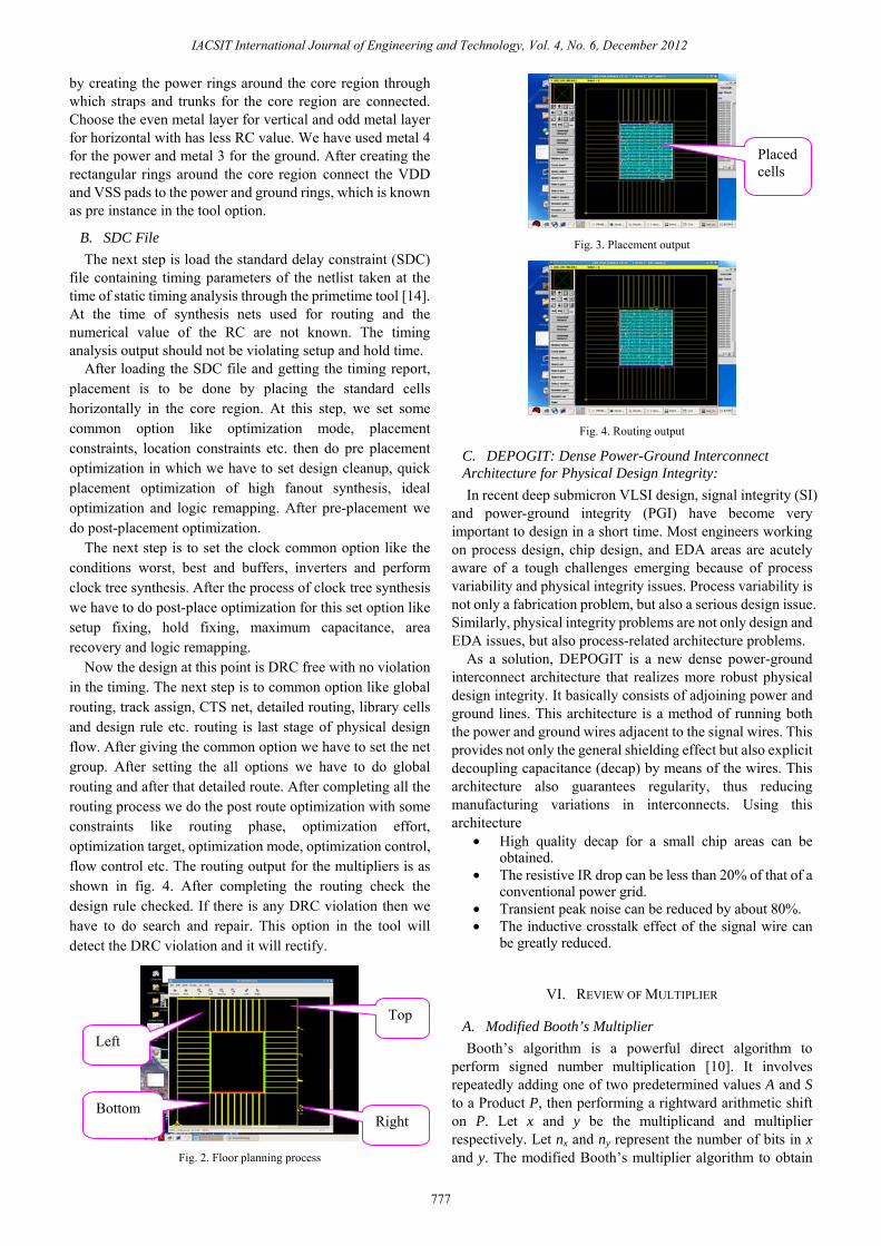
Now the design at this point is DRC free with no violation in the timing. The next step is to common option like global routing, track assign, CTS net, detailed routing, library cells and design rule etc. routing is last stage of physical design flow. After giving the common option we have to set the net group. After setting the all options we have to do global routing and after that detailed route. After completing all the routing process we do the post route optimization with some constraints like routing phase, optimization effort, optimization target, optimization mode, optimization control, flow control etc. The routing output for the multipliers is as shown in fig. 4. After completing the routing check the design rule checked. If there is any DRC violation then we have to do search and repair. This option in the tool will detect the DRC violation and it will rectify.
Fig. 2. Floor planning process
Fig. 3. Placement output
Fig. 4. Routing output
C. DEPOGIT: Dense Power-Ground Interconnect Architecture for Physical Design Integrity: In recent deep submicron VLSI design, signal integrity (SI)
and power-ground integrity (PGI) have become very important to design in a short time. Most engineers working on process design, chip design, and EDA areas are acutely aware of a tough challenges emerging because of process variability and physical integrity issues. Process variability is not only a fabrication problem, but also a serious design issue. Similarly, physical integrity problems are not only design and EDA issues, but also process-related architecture problems.
As a solution, DEPOGIT is a new dense power-ground interconnect architecture that realizes more robust physical design integrity. It basically consists of adjoining power and ground lines. This architecture is a method of running both the power and ground wires adjacent to the signal wires. This provides not only the general shielding effect but also explicit decoupling capacitance (decap) by means of the wires. This architecture also guarantees regularity, thus reducing manufacturing variations in interconnects. Using this architecture
• High quality decap for a small chip areas can be obtained.
• The resistive IR drop can be less than 20% of that of a conventional power grid.
• Transient peak noise can be reduced by about 80%. • The inductive crosstalk effect of the signal wire can
be greatly reduced.
VI. REVIEW OF MULTIPLIER
A. Modified Booth’s Multiplier Booth’s algorithm is a powerful direct algorithm to
perform signed number multiplication [10]. It involves repeatedly adding one of two predetermined values A and S to a Product P, then performing a rightward arithmetic shift on P. Let x and y be the multiplicand and multiplier respectively. Let nx and ny represent the number of bits in x and y. The modified Booth’s multiplier algorithm to obtain
Left
Top
Bottom Right
Placed cells
IACSIT International Journal of Engineering and Technology, Vol. 4, No. 6, December 2012
777

the product of x and y is as follows. 1) Determine the values of A, S and the initial value of P.
All of these numbers should have a length equal to nx + ny + 1.
• A: Fill the most significant (leftmost) bits with the value of x. Fill the remaining (ny +1) bits with zeros.
• S: Fill the most significant bits with the value of (-x) in two’s complement notation. Fill the remaining (ny +1) bits with zeros.
• P: Fill the most significant nx bits with zeros. To the right of this append the value of y. Fill the least significant (rightmost) bits with a zero
2) Determine the two least significant (rightmost) bits of P. • If they are 01, find the value of P+A, ignore any
overflow. • If they are 10, find the value of P+S, ignore any
overflow. • If they are 00 or 11, do nothing, use P directly in the
next step 3) Arithmetically shift the value obtained in the previous
step by a single place to the right. Let P now equal to this new value.
4) Repeat steps 2 and 3 until they have been done ny times. 5) Drop the least significant (rightmost) bit from P,
resultant is the product of x and y.
B. Wallace tree Multiplier In 1964 C.S.Wallace introduced a scheme for the
multiplication based on summing the partial product bits in parallel using a tree of carry save adders which became generally known as the Wallace tree [4]. This method has a three step process is used to multiply two numbers.
Step 1: The bit products are formed Step 2: The bit product matrix is reduced to a two row
matrix by using carry save adders known as Wallace tree. Step 3: The remaining two rows are summed using a fast
carry –propagate adder to produce the product. Though the process seems to be complex it yields
multipliers with delay proportional to the logarithm of the operand word length n. The Wallace tree multiplier belongs to a family of multipliers called column compression multipliers.
The principle in this family of multipliers is to achieve partial product accumulated by successively reducing the number of bits of information in each column using full adders or half adders. The full adder is known as (3:2) compressor because of its ability to add three bits from a single column of the partial product matrix and output two bits, one bit in the same column and one bit in the next column of the output matrix. The half adder is known as (2:2) compressor because of its ability to take two bits from a single column of the partial product matrix and output two bits, one bit in the next column of the output matrix.
Fig. 5 gives dot diagram of Wallace tree multiplier. The Wallace tree consists of numerous levels / stages of such column compressor structures until finally only two full width operands remain. These two operands can then be added using regular 2N bits adders to obtain the product result. The difference between the Wallace tree multiplier from column compression multiplier is that, in the Wallace tree every possible bit in every column is covered by the (3:2)
or (2:2) Compressors respectively. Until finally the partial product matrix has a depth of only two. Thus the Wallace tree multiplier uses as much hardware as possible to compress the partial product matrix as quickly as possible into the final product.
Fig. 5. Dot diagram of Wallace tree multiplier
C. Dadda Multiplier Dadda refined Wallace’s method by defining a counter
placement strategy that required fewer counters in the partial product reduction stage at the cost of a larger carry propagate adder [5]. Dadda has introduced a number of ways to compress the partial product bits using such a counter which later became known as Dadda’s Counter. Fig. 6 gives the process for 8 × 8 bits Dadda multiplier.
Fig. 6. Operation 8X8 bits dadda multiplier
An input 8 × 8 bits matrix of dots (each dot represents a bit) is shown as step 0. Columns having more than six dots are reduced by the use of half adders, each half adder takes in two dots and outputs one in the same column and one in the next more significant column and full adders, each full adder takes in three dots and outputs one in the same column and one in the next more significant column so that no column in step 1 will have more than six dots [5]. Half adders are shown by a crossed line in the succeeding matrix and full adders are shown by a line in the succeeding matrix. In each case the rightmost dot of the pair that is connected by a line is in the column from which the inputs were taken from the adder.
In the succeeding steps reduction to step 2 with no more than four dots per column, matrix three with no more than three dots per column, and finally step 4 with no more than two dots per column is performed. The height of the matrices is determined by working back from the final two row matrix and limiting the height of the each matrix to the largest integer that is no more than 1.5 times the height of its successor. Each matrix is produced from its predecessor in one adder delay. Since the number of bits in the words to be multiplied, the delay of the matrix reduction process that
IACSIT International Journal of Engineering and Technology, Vol. 4, No. 6, December 2012
778

reduces is proportional to log n, where n is word size. Since the adder that reduces the final two row matrix can be implemented as a carry look ahead adder which also has logarithmic delay, the total delay for this multiplier is proportional to the logarithm of the word size n.
VII. COMPARISON
A. Comparison of Dadda and Wallace Tree Multipliers This section gives the comparative study of the 8 X 8 bits
Dadda and Wallace tree multipliers. • Wallace tree multiplier uses 38 full adders and 15 half
adders. • Dadda multiplier uses 35 full adders and 7 half
adders. • Wallace tree multiplier requires a carry-propagate
adder of 10 bits wide • Dadda multiplier requires a carry propagate adder of
14 bits wide. • The other disadvantage of Dadda multiplier is that it
is less regular than the Wallace tree multiplier, making it more difficult to layout in VLSI design.
The multiplier being one of the major complex arithmetic building blocks for VLSI design has its own sets of complexities in terms of area, power, speed, and cost and design methodology.
The table III and table IV show the complexity involved in multiplier design. With bit width being increased, the number of stages also increases, and this introduces complexity. Wide bit width is required for accuracy and high sampling rate. Hence there is a need for design and development of an IP that can be easily adopted for any high speed applications by just using the basic building block of the multiplier design.
TABLE III: NUMBER OF STAGES IN MULTIPLIERS Bit width of Multiplier Number of Stages
2 0
3 1
4 2
5 to 6 3
7 to 9 4
10 to 13 5
14 to 19 6
20 to 28 7
29 to 42 8
43 to 63 9
64 o 94 10
TABLE IV: COMPARIAION OF MULTIPLIERS WITH RESPECT TO AREA, SPEED
AND POWER
Multiplier Delay (ns) Area (µm2)
Power (mw)
Dadda using carry look ahead adder 2.56 878 5.65
Dadda using Ripple carry adder 2.73 853 5.23
Array 8 3.02 979.7 5.16
Wallace 8 2.81 910 5.39
B. FPGA and ASIC The advantages of ASIC physical design over FPGA are
listed in table V.
TABLE V: COMPARIAION OF MULTIPLIERS WITH RESPECT TO AREA, SPEED AND POWER
Sl. No. FPGA ASIC
1 Complexity of multipliers is more
Complexity of multipliers is less
2 Area occupied by the multipliers is less.
Area occupied by the multipliers is more.
3 Power consumption by the multipliers is more.
Power consumption by the multipliers is less.
4 Delay is more and hence speed is less.
Delay is less and hence speed is high.
VIII. APPLICATION, CONCLUSION AND FUTURE WORK
A. Application The potential usages of proposed design are - • High Speed Signal Processing that includes DSP
based applications. • DWT and DCT transforms used for image and wide
signal processing. • FIR and IIR Filters for high speed, low power
filtering applications. • Multirate signal processing applications such as
digital down converters and up converters.
B. Conclusion In this work we have identified the techniques for optimal
computer aided designs of selected three 8 bits multipliers namely Booth, Wallace tree and Dadda by analyzing delay, area and power characteristics with particular emphasis on designing the cells for optimum power using layout design techniques. These three multipliers are implemented and the constraints area, power and timing are optimized using Verilog codes based on software resources NC SIM and VC SIM.
The results of the research work carried out are • Reviewed the existing high speed serial and parallel
multipliers available, identified the specification requirements for the multipliers.
• Modeled the multipliers using HDL and verified the functionality using test vectors.
• Implemented the design on FPGA and verified its functionality and identified the hardware requirements.
• Carried out ASIC design on the synthesized net list by appropriately providing the constraints based on the first cut information obtained from FPGA synthesis.
• Compared the performance of multiplier design and optimized the design for area, speed and power.
Finally we conclude that performance wise, Dadda multiplier consumes less area as compared to Wallace tree and Booth multiplier. Power wise Booth multiplier consumes less power compared to Wallace tree and Dadda multiplier. Delay wise Wallace tree has less delay as compared to Booth and Dadda multiplier.
From the tables we observed that the Dadda Multipliers requires more nets and consumes lesser references than Wallace tree multiplier and Booth multiplier. The increase in number of intermediate stages in multipliers, the
IACSIT International Journal of Engineering and Technology, Vol. 4, No. 6, December 2012
779

interconnection between the building blocks also increases. As Dadda multiplier has more number of intermediate stages it has more number of interconnections (76.5% more).
C. Scope for Future Work: As this work was limited to design of only the multiplier as
an IP using TSMC 130nm CMOS technology, it would be better to incorporate the Multiplier into a MAC unit that can perform multiplication and accumulation. MAC forms the major block for any filtering application. During the design of MAC block, redundancy in filter coefficients can be exploited to minimize the filter structure and optimize the performances of MAC unit. Also, there is possibility in developing a hybrid multiplier that takes into consideration both Dadda and Wallace multiplier architecture combined with booths multiplier.
REFERENCES [1] R. De Mori, “Suggestions for an IC fast parallel multiplier,”
Electronics letters, vol. 5, pp. 50-51, 1965. [2] C. L. Wey and T. Y. Chang, “Design and analysis of VLSI-based
parallel multipliers,” in Proc. IEEE proceedings Computers and Digital Techniques, vol. 137, no. 4, pp. 328-336, July 1990.
[3] T. K. Callaway and E. E. Swatzlander, “Optimizing multipliers for WSI,” in Proc. International Conference on Wafer Scale Integration, 1993, pp. 85-94.
[4] C. S. Wallace, “A suggestion for a fast multiplier,” IEE Transactions on Electronic Computers, vol. EC-13, pp. 14-17, 1964.
[5] L. Dadda, “Some schemes for parallel multipliers,” Alta Frequenza, vol. 34, pp. 349-356, August 1965.
[6] K. Adrea, C. Bickerstaff, M. J. Schulte, and E. E. S. Lander, “Reduced area multipliers,” in Proc. International Conference on Application Specific Array Processors, pp. 478-489, 1993.
[7] O. L. Mac Sorley, “High-speed arithmetic in binary computers,” in Proc. of the IRE, vol. 49, pp. 67-91, 1961.
[8] B. Gilchrist, J. H. Pomerene, and S. Y. Wong, “Fast carry logic for digital computers,” IRE Transactions on Electronic Computers, vol. 4, pp. 133-136, 1955.
[9] K. K. Parhi, VLSI digital signal processing systems design and implementation, ASIA: John Wiley and sons, 1999, vol. 5, pp. 323-346.
[10] A. D. Booth, “A signed binary multiplication technique,” Quarterly Journal of Mechanics and Applied Mathematics, vol. 4, pp. 236-240, 1951.
[11] R. F. Shaw, Arithmetic Operations in a Binary Computer: Review of Scientific Instruments, 1950, vol. 21, no. 9, pp. 687-693.
[12] C. R. Baugh and B. A. Wooley, “A two’s complement parallel array multiplication algorithm,” IEEE Transactions on Computers, vol. C-22, pp. 1045-1047, 1973.
[13] B. Parhami, Computer Arithmetic: Algorithms and Hardware Designs, Newyork: Oxford University press, 2000, vol. 4, pp. 245-256.
[14] H. Bhatnagar, Advanced ASIC Chip Synthesis, Second Edition: Kluwer Academic publisher, 2002, vol. 3-4, pp. 183-256.
Vasudev G. This author became a Member (M) of IAENG. He was born on 21 March 1985, has completed B.E from Nagarjuna college of Engineering and Technology,Bangalore, India in 2006, Completed his M.Tech from JSS Academy of Technical Education, Bangalore India, in the year 2008. Currently he is working as faculty in ACS College of Engineering, Bangalore, India. He is a member of IACSIT.
Rajendra Hegadi is Senior Member (80339644) of IAENG, born in Bijapur, state Karanataka. He has completed his Master of Science Degree in Solid State Physics from Gulbarga University, Gulbarga, Karnataka, India, Master Technology Degree in Computer Science and Engineering from National Institute of Technology Karnataka, Surathkal, India in 2000, Ph.D in Computer Science and Engineering from Dr. M.G.R. Educational
Research Institute University, Chennai, India in 2009. He has over 17 years of teaching in engineering education and 2 years of software industry experience. Currently he is working as Professor and Principal at Pragati College of Engineering and Management, Raipur (C.G), India since 2010. Dr. R. Hegadi is the Life Member of Cryptology Research Society of India (CRSI), Life member of Indian Society for Technical Education (ISTE), Member of The Society of Digital Information and Wireless Communications (SDIWC). He is Co-editor of CSVTU Research journal.
IACSIT International Journal of Engineering and Technology, Vol. 4, No. 6, December 2012
780