Description Pin Assignments - Diodes Incorporated The AL8808 is a step-down DC/DC converter designed...
20
AL8808 Document number: DS35648 Rev. 2 - 2 1 of 20 www.diodes.com January 2013 © Diodes Incorporated NEW PRODUCT AL8808 COST EFFECTIVE LOW EMI 30V 1A BUCK LED DRIVER Description The AL8808 is a step-down DC/DC converter designed to drive LEDs with a constant current. The device can drive up to 8 LEDs, depending on the forward voltage of the LEDs, in series from a voltage source of 6V to 30V. Series connection of the LEDs provides identical LED currents resulting in uniform brightness and eliminating the need for ballast resistors. The AL8808 switches at frequency up to 1MHz with controlled rise and fall times to reduce EMI. This allows the use of small size external components, hence minimizing the PCB area needed. Maximum output current of AL8808 is set via an external resistor connected between the V IN and SET input pins. Dimming is achieved by applying either an analog DC voltage or a PWM signal at the CTRL input pin. An input voltage of 0.4V or lower at CTRL switches off the output MOSFET simplifying PWM dimming. Applications • MR16 Lamps • General Illumination Lamps Pin Assignments Features • LED Driving Current Up to 1A • Better Than 5% Accuracy • High Efficiency Up to 96% • Fast Controlled Falling Edges 7ns • Operating Input Voltage from 6V to 30V • High Switching Frequency Up to 1MHz • PWM/DC Input for Dimming Control • Built-In Output Open-Circuit Protection • Built-In Over-Temperature Protection • TSOT25: Available in “Green” Molding Compound (No Br, Sb) Totally Lead-Free & Fully RoHS Compliant (Notes 1 & 2) Halogen and Antimony Free. “Green” Device (Note 3) Notes: 1. No purposely added lead. Fully EU Directive 2002/95/EC (RoHS) & 2011/65/EU (RoHS 2) compliant. 2. See http://www.diodes.com for more information about Diodes Incorporated’s definitions of Halogen and Antimony free, "Green" and Lead-Free. 3. Halogen and Antimony free "Green” products are defined as those which contain <900ppm bromine, <900ppm chlorine (<1500ppm total Br + Cl) and <1000ppm antimony compounds. Typical Applications Circuit TSOT25 (Top View) 1 2 3 5 4 V IN SET SW GND CTRL
Transcript of Description Pin Assignments - Diodes Incorporated The AL8808 is a step-down DC/DC converter designed...

AL8808 Document number: DS35648 Rev. 2 - 2
1 of 20 www.diodes.com
January 2013© Diodes Incorporated
NE
W P
RO
DU
CT
AL8808
COST EFFECTIVE LOW EMI 30V 1A BUCK LED DRIVER
Description The AL8808 is a step-down DC/DC converter designed to drive LEDs with a constant current. The device can drive up to 8 LEDs, depending on the forward voltage of the LEDs, in series from a voltage source of 6V to 30V. Series connection of the LEDs provides identical LED currents resulting in uniform brightness and eliminating the need for ballast resistors. The AL8808 switches at frequency up to 1MHz with controlled rise and fall times to reduce EMI. This allows the use of small size external components, hence minimizing the PCB area needed. Maximum output current of AL8808 is set via an external resistor connected between the VIN and SET input pins. Dimming is achieved by applying either an analog DC voltage or a PWM signal at the CTRL input pin. An input voltage of 0.4V or lower at CTRL switches off the output MOSFET simplifying PWM dimming.
Applications • MR16 Lamps • General Illumination Lamps
Pin Assignments
Features • LED Driving Current Up to 1A • Better Than 5% Accuracy • High Efficiency Up to 96% • Fast Controlled Falling Edges 7ns • Operating Input Voltage from 6V to 30V • High Switching Frequency Up to 1MHz • PWM/DC Input for Dimming Control • Built-In Output Open-Circuit Protection • Built-In Over-Temperature Protection • TSOT25: Available in “Green” Molding Compound (No Br, Sb)
Totally Lead-Free & Fully RoHS Compliant (Notes 1 & 2) Halogen and Antimony Free. “Green” Device (Note 3)
Notes: 1. No purposely added lead. Fully EU Directive 2002/95/EC (RoHS) & 2011/65/EU (RoHS 2) compliant. 2. See http://www.diodes.com for more information about Diodes Incorporated’s definitions of Halogen and Antimony free, "Green" and Lead-Free. 3. Halogen and Antimony free "Green” products are defined as those which contain <900ppm bromine, <900ppm chlorine (<1500ppm total Br + Cl) and <1000ppm antimony compounds.
Typical Applications Circuit
TSOT25
(Top View)
1
2
3
5
4
VIN
SET
SW
GND
CTRL

NE
W P
RO
DU
CT
AL8808 Document number
Pin Descri
Pin Number 1 2
3
4
5
Functiona
Absolute M
Symbol ESD HBM ESD MM
VIN VSET VSW
VCTRL ISW TJ
TLEAD TST
Caution: StressefunctionaffecteSemicoand tra
r: DS35648 Rev. 2
iptions
Pin Name SW
GND
CTRL
SET
VIN
al Block Dia
Maximum
Human Body MMachine ModeContinuous VI
SET pin voltagSW voltage reCTRL pin inpuSwitch currentJunction TempLead TemperaStorage Temp
es greater than thenal operation of thed by exposure to aonductor devices a
ansporting these de
- 2
Switch Pin. CGND Pin Dimming and• Leave f
(V• Drive to• Drive w
IOUTnom
• Drive w• A PWM
current Set Nominal Input Supply section for m
agram
Ratings (@
Model ESD Proteel ESD Protectio
N pin voltage relage relative to VIN
elative to GND ut voltage t perature ature Soldering perature Range
e 'Absolute Maxime device at these obsolute maximum
are ESD sensitive aevices.
w
Connect inductor
d On/Off Control floating for normaVCTRL = 5V, Giveo voltage below 0ith an analog vol
m ith an analog vol signal (low leveto be adjusted bOutput Current PPin. Must be loc
more information.
Figure 1
TA = +25°C, unle
Parameterection n ative to GND pin
mum Ratings' specor any other conditrating conditions foand may be damag
2 of 20 www.diodes.co
r/freewheeling dio
Input. al operation.
es nominal avera0.4V to turn off oultage (0.5V < VCT
ltage > 2.6V outpl ≤ 0.4V and high
below the level sePin. Configure thcally decoupled t
. AL8808 Block
ess otherwise sp
ified above, may ctions exceeding thoor extended periodsged by exposure to
m
Function ode here, minimi
ge output currenutput current TRL < 2.5V) to ad
put current will beh level > 2.6; tranet by the resistor
he output current o GND with > 2.2
k Diagram
pecified.)
cause permanent dose indicated in this of time. o ESD events. Suit
izing track length
nt IOUTnom = 0.1/R
djust output curre
e 100% of IOUTnonsition times lessr connected to Sof the device.
2µF X7R cerami
Rating2.5 200
-0.3 to -5 to +
-0.3 to -0.3 to
1.25150300
-55 to +
damage to the devis specification is n
table ESD precaut
h at this pin to red
RS)
ent from 20% to
om s than 1µs) allowET input pin.
c capacitor – see
gs
0 +33 0.3 +33 +6
5 0 0 +150
vice. These are stnot implied. Device
ions should be tak
January 201© Diodes Incorporate
AL8808
duce EMI.
100% of
ws the output
e applications
Unit kV V V V V V A °C °C °C
tress ratings only; e reliability may be
ken when handling
3ed

AL8808 Document number: DS35648 Rev. 2 - 2
3 of 20 www.diodes.com
January 2013© Diodes Incorporated
NE
W P
RO
DU
CT
AL8808
Recommended Operating Conditions (@TA = +25°C, unless otherwise specified.)
Symbol Parameter Min Max Unit
VIN Operating Input Voltage Relative to GND 6.0 30 V VCTRLH Voltage High for PWM Dimming Relative to GND 2.6 5.5 V VCTRLDC Voltage Range for 20% to 100% DC Dimming Relative to GND 0.5 2.5 V VCTRLL Voltage Low for PWM Dimming Relative to GND 0 0.4 V
ISW Continuous Switch Current (Note 4) 1 A fSW Maximum Switching Frequency 1 MHz TJ Junction Temperature Range -40 +125 °C
Note: 4. Subject to ambient temperature, input voltage and switching frequency. See applications section for suggested derating.
Electrical Characteristics (@ TA = +25°C, VIN = 12V, CTRL pin floating; unless otherwise specified.)
Symbol Parameter Conditions Min Typ Max Unit VINSU Internal Regulator Start Up Voltage VIN rising 5.6 V VINSH Internal Regulator Hysteresis Threshold VIN falling 200 mV
IQ Quiescent Current VIN = 30V, output not switching 350 µA IS Input Supply Current fSW = 250kHz 450 µA
VTH Set Current Threshold Voltage 95 100 105 mV VTH-H Set Threshold Hysteresis ±20 mV ISET SET Pin Input Current VSET = VIN -0.1 16 µA
VCTRL Open Circuit CTRL Pin Voltage 5 V RCTRL CTRL Pin Input Resistance Referred to internal 5V regulator. 50 kΩ VREF Internal Reference Voltage 2.5 V
RDS(on) On Resistance of SW MOSFET ISW = 0.35A 0.35 Ω ISW_Lkg Switch Leakage Current VIN = 30V, VCTRL = 0.4V, VSENSE = 0V 0.5 µA
tR SW Rise Time VSENSE = 100 ±20mV, fSW = 250kHz VSW = 0.1V to 12V to 0.1V, CL = 15pF
7 ns
tF SW Fall Time 5 ns
TOTP Over-Temperature Shutdown
145 °C TOTP-Hyst Over-Temperature Hysteresis 10 °C
θJA Thermal Resistance Junction-to-Ambient TSOT25 (Note 5) 209 °C/W θJL Thermal Resistance Junction-to-Lead TSOT25 (Note 5) 57
θJT Thermal Resistance Junction-to-Top TSOT25 (Note 5) 13
Notes: 5. Device mounted on FR-4 PCB (25mm x 25mm 1oz copper, minimum recommended pad layout on top layer and thermal vias to maximum area bottom layer ground plane. For better thermal performance, larger copper pad for heat-sink is needed. …Refer to Figure 42 for the device derating curve.

AL8808 Document number: DS35648 Rev. 2 - 2
4 of 20 www.diodes.com
January 2013© Diodes Incorporated
NE
W P
RO
DU
CT
AL8808
Typical Performance Characteristics (@ TA = +25°C, unless otherwise stated.)
0 3 6 9 12 15 18 21 24 27 30INPUT VOLTAGE (V)
Figure 2. Supply Current vs. Input Voltage
400
350
300
250
200
150
100
50
0
INP
UT
CU
RR
EN
T (µ
A)
V = 0VV = VT = +25°C
CTRL
SET IN
A
L = 33µH T = +25°CV = 12VR = 150m1 LED
A
IN
SET
Ω
L = 68µH
L = 100µH
0.0 0.5 1.0 1.5 2.0 2.5 3.0 3.5 4.0 4.5 5.0 VCTRL (V)
Figure 3. Switching Frequency vs. VCTRL
900
800
700
600
500
400
300
100
0
FRE
QU
EN
CY
(kH
z)
200
T = +25°CV = 12VL = 68µH
A
IN
1 LED
RSET = 100mΩ
RSET = 150mΩ
RSET = 300mΩ
0.0 0.5 1.0 1.5 2.0 2.5 3.0 3.5 4.0 4.5 5.0 VCTRL (V)
Figure 4. LED Current vs. VCTRL
1.2
1.0
0.8
0.6
0.4
0.2
0.0
LED
CU
RR
EN
T (A
)
0.0 0.5 1.0 1.5 2.0 2.5 3.0 3.5 4.0 4.5 5.0VCTRL (V)
Figure 5. I vs. VCTRL CTRL
20
0
-20
-40
-60
-80
-100
-120
CTR
L P
IN C
UR
RE
NT
(µA
)T = +25°C, V = 12VL = 68µH, R
A IN
SET = 150m1 LED
Ω
0 20 40 60 80 100PWM DUTY CYCLE (%)
Figure 6. I vs. PWM Duty CycleLED
6
5
4
3
2
1
0
LED
CU
RR
EN
T E
RR
OR
(%)
0.9
LED
CU
RR
EN
T(A
)
0.6
0.3
0.0
T = +25°C, V = 12VL = 68µH, R
A IN
SET
PWM
= 150m1 LED, f = 500Hz
Ω
6 9 12 15 18 21 24 27 30INPUT VOLTAGE VCTRL (V)
Figure 7. Duty Cycle vs. Input Voltage
100
90
70
60
40
30
10
0
DU
TY C
YC
LE (%
)
80
50
20T = +25°C, R = 150mL = 33µH, L = 68µH, L = 100µH
A SET Ω

NE
W P
RO
DU
CT
AL8808 Document number
Typical Pe
SW
MO
SFE
T R
(m)
DS
(ON
)Ω
60
50
40
30
20
10
0.50
0.45
0.40
0.35
0.30
0.25
0.20
0.15
0.00
0.05
0.10
SW
MO
SFE
T R
()
DS
(ON
)Ω
r: DS35648 Rev. 2
erformance
Figure 12. S
-40 -25 -10 5AMBI
Figure 8.
00
00
00
00
00
0
00
V = OpenV = V = 12
CTRL
SET IN
0 200
0
5
0
5
0
5
0
5
0
5
0
SWFigure 10.
V = 12VV = VT = +25°CCTRL = Floating
IN
SET IN
A
- 2
e Characte
Steady State Wa
50 6520 35ENT TEMPERAT SW R vsDS(ON)
2V
400 600
WITCH CURRENTSW R vs. SDS(ON)
w
eristics (cont
aveforms
5 80 95 110 1TURE (°C). Temperature
800 1
T (mA)Switch Current
5 of 20 www.diodes.co
t.) (@ TA = +25°C
25
000
m
C, unless otherw
Figu
Figur
6 9
Fig
SW
MO
SFE
T R
(m)
DS
(ON
)Ω
400
350
300
250
200
0
100
150
50V =V = VT = 25°
CTRL
SET
A
wise stated.)
ure 11. SW Outp
re 13. SW Outp
12 15 18V
ure 9. SW RIN
DS(O
= OpenV°C
IN
put Fall Time
ut Rise Time
21 248(V)
vs. Input VoltaON)
January 201© Diodes Incorporate
AL8808
27 30
age
3ed

AL8808 Document number: DS35648 Rev. 2 - 2
6 of 20 www.diodes.com
January 2013© Diodes Incorporated
NE
W P
RO
DU
CT
AL8808
Typical Performance Characteristics (L = 68µH, TA = +25°C, unless otherwise stated.)
6 9 12 15 18 21 24 27 30INPUT VOLTAGE (V)
Figure 14. Efficiency vs. Input Voltage
100
95
90
85
80
75
70
EFFI
CIE
NC
Y (%
)
1 LED
2 LEDs
3 LEDs4 LEDs 5 LEDs
7 LEDs
T = 25°CL= 68µHR = 150m
A
SET Ω
1 LED
2 LEDs 3 LEDs 4 LEDs 5 LEDs7 LEDs
6 9 12 15 18 21 24 27 30INPUT VOLTAGE (V)
Figure 15. 330mA LED Current vs. Input Voltage
0.36
0.35
0.34
0.33
0.32
0.31
0.30
LED
CU
RR
EN
T (A
)
T = 25°CL= 68µHR = 300m
A
SET Ω
6 9 12 15 18 21 24 27 30INPUT VOLTAGE (V)
Figure 16. Switching Frequency vs. Input Voltage
450
400
300
200
100
50
0
SW
ITC
HIN
G F
RE
QU
EN
CY
(kH
z)
350
250
1501 LED
2 LEDs 3 LEDs 4 LEDs 5 LEDs7 LEDs
6 9 12 15 18 21 24 27 30INPUT VOLTAGE (V)
Figure 17. 670mA LED Current vs. Input Voltage
0.74
0.72
0.70
0.66
0.64
0.62
0.60
LED
CU
RR
EN
T (A
)
0.68
T = 25°C, VL= 68µH, R = 150m
A
SET
IN = 12VΩ
1 LED
2 LEDs 3 LEDs
4 LEDs
5 LEDs
7 LEDs
6 9 12 15 18 21 24 27 30INPUT VOLTAGE (V)
Figure 18. Duty Cycle vs. Input Voltage
100
90
70
40
20
10
0
DU
TY C
YC
LE (%
)
80
60
30
50
1 LED
2 LEDs
3 LEDs
4 LEDs 5 LEDs 7 LEDs
T = 25°CL= 68µHR = 150m
A
SET Ω
6 9 12 15 18 21 24 27 30INPUT VOLTAGE (V)
Figure 19. 1A LED Current vs. Input Voltage
1 LED
2 LEDs
3 LEDs
4 LEDs5 LEDs
7 LEDs
T = 25°CL= 68µHR = 100m
A
SET Ω
1.10
1.05
0.95
0.90
LED
CU
RR
ENT
(A)
1.00

AL8808 Document number: DS35648 Rev. 2 - 2
7 of 20 www.diodes.com
January 2013© Diodes Incorporated
NE
W P
RO
DU
CT
AL8808
Typical Performance Characteristics (670mA LED Current; TA = +25°C unless otherwise stated.)
186 9 12 15 21 24 27 30INPUT VOLTAGE (V)
Figure 20. LED Current Deviation vs. Input Voltage
DE
VIA
TIO
N F
RO
M T
AR
GE
T C
UR
RE
NT
(%) 5
3
-3
-5
1
-1
4 LEDs
5 LEDs
7 LEDs
1 LED
2 LEDs 3 LEDs
T = 25°C,L = 33µHR = 150m
A
SET Ω
186 9 12 15 21 24 27 30INPUT VOLTAGE (V)
Figure 21. Switching Frequency vs. Input Voltage
SW
ITC
HIN
G F
RE
QU
EN
CY
(kH
z)
500
400
100
0
300
200
800
700
600
4 LEDs 5 LEDs7 LEDs
1 LED
2 LEDs 3 LEDs
T = 25°C,L = 33µHR = 150m
A
SET Ω
186 9 12 15 21 24 27 30INPUT VOLTAGE (V)
Figure 22. LED Current Deviation vs. Input Voltage
DE
VIA
TIO
N F
RO
M T
AR
GE
T (%
)
2
1
-2
-5
0
-1
5
4
3
-4
-3
4 LEDs5 LEDs
7 LEDs
1 LED
2 LEDs3 LEDs
T = 25°C,L = 68µHR = 150m
A
SET Ω
186 9 12 15 21 24 27 30INPUT VOLTAGE (V)
Figure 23. Switching Frequency vs. Input Voltage
SW
ITC
HIN
G F
RE
QU
EN
CY
(kH
z)
300
250
50
0
200
150
450
400
350
100
T = 25°C,L = 100µHR = 150m
A
SET Ω
4 LEDs 5 LEDs
7 LEDs
1 LED
2 LEDs3 LEDs
186 9 12 15 21 24 27 30INPUT VOLTAGE (V)
Figure 24. LED Current Deviation vs. Input Voltage
DE
VIA
TIO
N F
RO
M T
AR
GET
(%)
2
1
-2
-5
0
-1
5
4
3
-4
-3
186 9 12 15 21 24 27 30INPUT VOLTAGE (V)
Figure 25. Switching Frequency vs. Input Voltage
SW
ITC
HIN
G F
RE
QU
EN
CY
(kH
z)
150
0
100
250
200
50

AL8808 Document number: DS35648 Rev. 2 - 2
8 of 20 www.diodes.com
January 2013© Diodes Incorporated
NE
W P
RO
DU
CT
AL8808
Typical Performance Characteristics (1A LED Current) TA = +25°C unless otherwise stated.)
1 LED
2 LEDs3 LEDs 4 LEDs 5 LEDs 7 LEDs
T = 25°CL = 33µHR = 100m
A
SET Ω
1815126 9 30272421INPUT VOLTAGE (V)
Figure 26. LED Current Deviation vs. Input Voltage
5
4
3
2
-4
-5
0
DE
VIA
TIO
N F
RO
M T
AR
GET
CU
RR
ENT
(%)
1
-1
-2
-3
1815126 9 30272421INPUT VOLTAGE (V)
Figure 27. Switching Frequency vs. Input Voltage
600
500
400
300
100
0
200
SWIT
CH
ING
FR
EQ
UE
NC
Y (k
Hz)
1 LED
2 LEDs 3 LEDs 4 LEDs 5 LEDs 7 LEDs
T = 25°CL = 33µHR = 100m
A
SET Ω
1815126 9 30272421INPUT VOLTAGE (V)
Figure 28. LED Current Deviation vs. Input Voltage
1 LED
2 LEDs
3 LEDs4 LEDs
5 LEDs7 LEDs
T = 25°CL = 68µHR = 100m
A
SET Ω
5
4
3
2
-4
-5
0
DE
VIAT
ION
FR
OM
TAR
GE
T C
UR
REN
T (%
)
1
-1
-2
-3
1815126 9 30272421INPUT VOLTAGE (V)
Figure 29. Switching Frequency vs. Input Voltage
300
250
200
150
50
0
100
SW
ITC
HIN
G F
RE
QU
ENC
Y (k
Hz)
1815126 9 30272421INPUT VOLTAGE (V)
Figure 30. LED Current Deviation vs. Input Voltage
1 LED
2 LEDs 3 LEDs4 LEDs
5 LEDs 7 LEDs
T = 25°CL = 100µHR = 100m
A
SET Ω
5
4
3
2
-4
-5
0
DE
VIA
TIO
N F
RO
M T
AR
GE
T C
UR
RE
NT
(%)
1
-1
-2
-3
1815126 9 30272421INPUT VOLTAGE (V)
Figure 31. Switching Frequency vs. Input Voltage
200
180
160
80
20
0
60
SW
ITC
HIN
G F
RE
QU
EN
CY
(kH
z)
140
100
120
40
1 LED
NE
W P
RO
DU
CT
AL8808 Document number
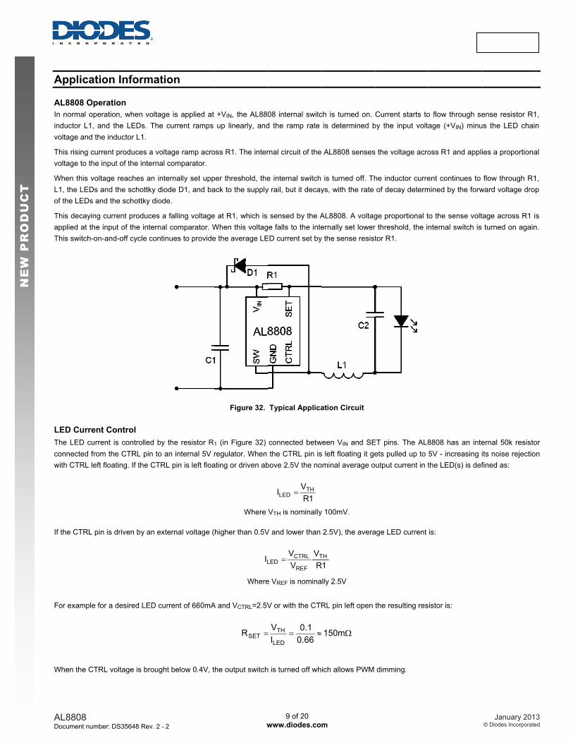
Applicatio AL8808 OperaIn normal operainductor L1, andvoltage and the
This rising currevoltage to the in
When this voltagL1, the LEDs anof the LEDs and
This decaying capplied at the inThis switch-on-a
LED Current CThe LED currenconnected from with CTRL left flo
If the CTRL pin i
For example for
When the CTRL
r: DS35648 Rev. 2
on Informat
ation ation, when voltad the LEDs. Theinductor L1.
ent produces a voput of the interna
ge reaches an innd the schottky dd the schottky dio
urrent produces nput of the internand-off cycle con
Control nt is controlled b
the CTRL pin tooating. If the CT
is driven by an e
a desired LED c
L voltage is broug
- 2
tion
age is applied at e current ramps
oltage ramp acroal comparator.
nternally set uppdiode D1, and baode.
a falling voltageal comparator. Wtinues to provide
by the resistor Ro an internal 5V rRL pin is left floa
xternal voltage (
current of 660mA
ght below 0.4V, t
w
+VIN, the AL880up linearly, and
oss R1. The inter
per threshold, theack to the supply
e at R1, which is When this voltage the average LE
Figure 32.
1 (in Figure 32) regulator. When ating or driven ab
Where
higher than 0.5V
IL
Where
A and VCTRL=2.5V
=RSET
he output switch
9 of 20 www.diodes.co
08 internal switcd the ramp rate
rnal circuit of the
e internal switch y rail, but it decay
sensed by the Ae falls to the inte
ED current set by
Typical Applica
connected betwthe CTRL pin is
bove 2.5V the no
1RVI TH
LED =
VTH is nominally
V and lower than
RV
VV T
REF
CTRLLED =
e VREF is nomina
V or with the CTR
≈==66.01.0
IV
LED
TH
h is turned off wh
m
ch is turned on. is determined b
AL8808 senses
is turned off. Thys, with the rate
AL8808. A voltagernally set lower
y the sense resist
ation Circuit
ween VIN and SEs left floating it geominal average o
y 100mV.
2.5V), the avera
1RTH
ally 2.5V
RL pin left open
Ωm150
ich allows PWM
Current starts toby the input volta
s the voltage acro
he inductor curreof decay determ
ge proportional tor threshold, the intor R1.
ET pins. The AL8ets pulled up to 5utput current in t
age LED current
the resulting res
dimming.
o flow through seage (+VIN) minu
oss R1 and appli
ent continues to mined by the forw
o the sense voltnternal switch is
8808 has an inte5V - increasing ithe LED(s) is def
is:
istor is:
January 201© Diodes Incorporate
AL8808
ense resistor R1us the LED chain
ies a proportiona
flow through R1ward voltage drop
age across R1 isturned on again
ernal 50k resistoits noise rejectiofined as:
3ed
, n
al
, p
s n.
or n

AL8808 Document number: DS35648 Rev. 2 - 2
10 of 20 www.diodes.com
January 2013© Diodes Incorporated
NE
W P
RO
DU
CT
AL8808
Application Information (cont.) Analog Dimming The CTRL pin can be driven by an external analog voltage (VCTRL), to adjust the output current to a value below the nominal average value defined by R1. The LED current decreases linearly with the CTRL voltage when 0.5V ≤ VCTRL ≤ 2.5V.
Note that 100% brightness is achieved when either the CTRL pin is left floating or pulled above 2.5V by an external voltage source.
For 2.6V ≤ VCTRL ≤ 5.5V the LED current will not get overdriven and will be set the current according to the equation VCTRL = 2.5V (the internal reference voltage). See Figure 33 below.
PWM Dimming LED current can be adjusted digitally, by applying a low frequency Pulse Width Modulated (PWM) logic signal to the CTRL pin to turn the device on and off. This will produce an average output current proportional to the duty cycle of the control signal. In particular, a PWM signal with a max resolution of 10bit (~0.1% duty cycle) can be applied to the CTRL pin to change the output current to a value below the nominal average value set by resistor RSET. To achieve this resolution the PWM frequency has to be lower than 500Hz, however higher dimming frequencies can be used, at the expense of dimming dynamic range and accuracy. Typically, for a PWM frequency of 500Hz the accuracy is better than 2% for PWM ranging from 5% to 100%.
0.0 0.5 1.0 1.5 2.0 2.5 3.0 3.5 4.0 4.5 5.0V (V)
Figure 33. LED Current Dimming Ration andTypical Error vs. Control Voltage
CTRL
110
100
90
80
70
60
50
40
30
20
10
0
DIM
ME
D :
100%
LE
D C
UR
RE
NT
RAT
IO (%
)
LED Current Error
Dimmed LED Current Ratio2.0
2.2
0.0
0.2
0.4
0.6
0.8
1.0
1.2
1.4
1.6
1.8
TYP
ICA
LE
RR
OR
(%)
T = 25°CV = 12VL = 68µH
A
IN
50 600 10 20 30 40 90 10070 80PWM DUTY CYCLE (%)
Figure 34. PWM Dimming at 500Hz
0.8
0.7
0.1
0
0.3
0.2
0.6
0.5
0.4
LED
CU
RR
EN
T (A
)
V = 12VT = +25°CL = 68µHR = 150m1 LED
IN
A
SET Ω
V = 12VT = +25°CL = 68µHR = 150m1 LED
IN
A
SET Ω
7.50.0 2.5 5.0 15.010.0 12.5PWM DUTY CYCLE (%)
Figure 35. Low Duty Cycle PWM Dimming at 500Hz
LOAD
CU
RR
EN
T E
RR
OR
(%)
10
9
8
7
6
5
4
3
2
1
10

NE
W P
RO
DU
CT
AL8808 Document number
Applicatio PWM DimminThe CTRL pin isoutput stage. The ultimate PWlower switching the accuracy/line At the start of ethreshold isn’t re
Greater PWM dfrequency. The three figurefrom a 12V rail a
Figure 36. 0
Figure 38. 0
As can be obsevalue.
r: DS35648 Rev. 2
on Informat
ng (cont.) s designed to be
WM dimming resofrequencies andearity of the PWM
each PWM cycleeached then the
dimming dynami
s below show 0.at +25°C for a no
.2% PWM Duty 68µH
.2% PWM Duty 22µH
rved from Figure
- 2
tion (cont.)
e driven by both
olution is determ/or higher PWM M dimming.
e the LED curreaccuracy will be
c ranges can be
2% duty cycle Pominal LED curre
Cycle at 100Hz H Inductance
Cycle at 500Hz H Inductance
e 37 greater dim
w
3.3V and 5V log
ined by the numfrequencies the
ent needs to resgreatly affected.
e achieved by r
PWM pulse resolent of 670mA.
PWM Frequenc
PWM Frequenc
mming accuracy c
11 of 20 www.diodes.co
gic levels directly
ber of full LED snumber of full sw
start from zero u. reducing the PW
ution with differe
cy and Fig
cy and
can be achieved
m
y from a logic ou
switching cycles twitching cycles t
up to the upper
WM dimming fre
ent PWM frequen
gure 37. 0.2% P
d by reducing bo
tput with either a
that can be achiethat can be achie
r threshold level
quency and/or i
ncies and differe
WM Duty Cycle22µH Indu
th the PWM dim
an open drain ou
eved during the eved is reduced
(nominally 120
ncreasing the A
nt inductor value
e at 100Hz PWMuctance
mming frequency
January 201© Diodes Incorporate
AL8808
utput or push pu
PWM on-time. Athereby reducing
mV/RSET). If this
AL8808 switching
es driving 2 LEDs
Frequency and
and the inducto
3ed
ll
At g
s
g
s
d
or

NE
W P
RO
DU
CT
AL8808 Document number
Applicatio Start-up and SOn initial power than 0.45V (typithe output starts
This will cause sthe upper LED c The AL8808 doeaccuracy.
Soft start can berail on the CTRL
The external capoccurs it is esse
This is achievedthe control volta Adding this capadimming accura
Reducing OutPeak to peak ripA value of 1μF capacitor values Note that the cavoltage. By addaltering the mea
r: DS35648 Rev. 2
on Informat
Soft Start up the device w
cal). This causess switching the LE
some additional icurrent threshold
es not have in-bu
e easily implemeL pin will charge t
pacitor slows upntial that the cap
d by increasing thge at the input of
acitor increases cy depending on
Figure
tput Ripple pple current in the
will reduce the s.
apacitor will not ing this capacito
an current value.
- 2
tion (cont.)
will not start switcs a slight delay (ED current will b
nput current to thlevel by slowing
uilt soft-start acti
ented by adding athe external capa
the ramp-up of pacitor is large en
he time taken forf the comparator
the time taken fn the delay introd
39. Soft Start w
e LED(s) can be supply ripple c
affect operatingor the current wa
w
ching until the p(dependent on rauild up to the upp
ILEDS
hat of charging thg down the rise o
ion allowing very
an external capaacitor up to 5V.
the CTRL pin vonough to keep th
r the CTRL voltar.
for the output toduced.
with 100nF Cap
reduced, if requurrent significan
g frequency or eaveform through
12 of 20 www.diodes.co
ower supply hasamp rate of inpuper threshold lev
1.0V5.2
VCTRLSSPK =
he input bulk capf the CTRL pin v
y fast control of t
acitor from the C
oltage thereby rehe CTRL pin volta
age to rise to the
o reach 90% of i
pacitor on CTRL
ired, by shuntingntly in the typica
efficiency, but it wthe LED(s) chan
m
s reached approxt voltage and inp
vel:
1R2.11×
pacitance. One wvoltage – implem
the output Power
CTRL pin to groun
educing the LEDage below 2.5V d
upper (turn-off)
ts final value, th
L pin (VIN = 24V,
g a capacitor C2 al case. Proportio
will increase stanges from a trian
ximately 5.6V orput bulk capacita
way of reducing tenting a soft-sta
r MOSFET switc
nd. The internal
current via analduring the ramp-
threshold and by
his delay is 25µs
ILED = 667mA, 1
across the LED(onally lower ripp
art-up delay, by ngular ramp to a
r the CTRL pin vance of the AL88
this additional curt.
ch which improve
pull-up resistor t
log dimming. To -up of the input v
y slowing down t
s/nF, but will imp
1 LED)
(s) as shown in Fple can be achie
reducing the rata more sinusoida
January 201© Diodes Incorporate
AL8808
voltage is greate808 circuit). Once
urrent is to reduce
es PWM dimming
to the internal 5V
ensure soft-starvoltage.
the rate of rise o
pact on the PWM
Figure 32. eved with highe
te of rise of LEDal version withou
3ed
er e
e
g
V
rt
of
M
er
D ut

NE
W P
RO
DU
CT
AL8808 Document number
Applicatio Inductor SeleRecommended data for selecterequired switchiLED current acc
The inductor shoThe chosen coil required mean o
Suitable coils for
Part
MSS1038-333
MSS1038-683
NPIS64D330M The inductor valThe following eq Switch ‘On’ tim
V
tIN
ON −=
Switch ‘Off’ tim
V
tL
OFF =
Where:
L is the coil rL is the coil RS is the curIavg is the reVIN is the suΔI is the coilVLED is the tRSW is the sVD is the dio
r: DS35648 Rev. 2
on Informat
ection inductor values
ed component vang frequency. L
curacy (due to pro
ould be mountedshould have a s
output current.
r use with the AL
No.
MTRF
ue should be choquations can be u
me:
xIVL
AVGLED −−Δ
me:
IVIL
AVGDLED ++Δ
inductance (H) resistance (Ω) rrent sense resisquired LED curre
upply voltage (V) l peak-peak rippltotal LED forwardswitch resistanceode forward volta
- 2
tion (cont.)
for the AL8808 alues. The inducLower inductor vopagation delays
Figure 4
d as close to the dsaturation current
L8807 are listed iL
(µH) D(
33 0.
68 0.
33 0.
osen to maintainused as a guide,
( RrRxI
SWLS ++
( )rRx LSG +
stance (Ω) ent (A)
e current (A) Intd voltage (V) (Ω) =0.35Ω nom
age at the require
w
are in the rangectance used willalues can be uss) and increase p
0. Inductor Valu
device as possibt higher than the
in the table belowDCR (V)
ISAT(A)
093 2.3
213 1.5
124 1.1
n operating duty c with reference t
)W
ternally set to 0.4
minal ed load current (V
13 of 20 www.diodes.co
e 33µH to 100µH depend on a c
sed to increase tpower dissipation
ue with Input Volt
ble with low resispeak output cur
w: T )
3 Co
5
1
cycle and switcho Figure 1 - Ope
4 x IAVG
V)
m
H. Note that thecombination of Inhe switching freqn (due to switchin
tage and Numbe
stance/stray inducrrent and a contin
Manufactu
oilCraft www.coi
NIC www.niccom
'on'/'off' times overating waveform
Figure
e AL8808 Web Cnput voltage andquency and redung losses).
er of LEDs
ctance connectionuous current rat
rer
lcraft.com
mp.com
ver the supply voms.
e 41. Typical Swi
Calculator providd LED chain vouce solution size
ons to the SW piting above the
oltage and load c
itching Waveform
January 201© Diodes Incorporate
AL8808
es performance ltage to set the
e but may affect
n.
current range.
m
3ed

AL8808 Document number: DS35648 Rev. 2 - 2
14 of 20 www.diodes.com
January 2013© Diodes Incorporated
NE
W P
RO
DU
CT
AL8808
Application Information (cont.) Capacitor Selection The small size of ceramic capacitors makes them ideal for AL8808 applications. X7R type is recommended because it retains capacitance value over wider voltage and temperature ranges than other types such as Y5V or Z5U. X5R is a useful compromise over a restricted temperature range. Note that even X7R capacitance reduces significantly with increased DC bias voltage. At 50% of rated voltage, the capacitance loss is between about 10% to 50% of nominal. Therefore it is often necessary to select a voltage rating which is at least twice the operating voltage. Input Capacitor In Figure 32, the input capacitor C1 is required as a reservoir. Diode D1 switches at a rate of typically up to 400kHz. The power supply has a finite impedance, often including a wiring inductance value of the order of 100nH to 1uH or more depending upon the system design. C1 is required to limit the power supply voltage and current ripple both to allow stable regulation of the LED current, and also to meet EMC requirements. A 2.2μF input capacitor is sufficient for most DC powered applications of AL8808. This depends upon the operating voltage and current and the maximum level of ripple required. Additional capacitors may be required in parallel for EMC purposes. This is described below in a separate section. However, if operated from a rectified low voltage AC source, such as MR16, then the input capacitance will need to be significantly increased to provide enough reservoir charge when the input voltage falls below the minimum operating voltage of the AL8808 or the LED chain voltage Output Capacitor In Figure 32, the output capacitor C2 is normally required to limit the load voltage and current ripple, in order to meet EMC requirements. A value of 0.1µF to 1µF is sufficient for many requirements, depending on voltage and current conditions. Additional capacitors may be required in parallel for EMC purposes. This is described below in a separate section. Diode Selection For maximum efficiency and performance, the flywheel rectifier (D1) should be a fast low capacitance Schottky diode with low reverse leakage at the maximum operating voltage and temperature. The silicon PN diode is not suitable because of its increased power loss, due to a combination of lower forward voltage and reduced recovery time. The use of a Super-Barrier-Rectifier (SBR) is not recommended for use as a flywheel diode in this application. (However the SBR provides significant advantages when used with an AC power input as a bridge rectifier driving VIN.)
It is important to select D1 with a peak current rating above the peak coil current and a continuous current rating higher than the maximum output load current. In particular, it is recommended to have a diode voltage rating at least 15% higher than VIN to ensure safe operation during the switching and a mean current rating at least 10% higher than the peak diode current. The power rating is verified by calculating the power loss through the diode. In practice, the voltage rating selection is often increased by up to about 50% to obtain a better compromise with loss due to reverse leakage current at higher temperature. Also the current rating is typically selected to provide a margin of up to about 50%. Schottky diodes, e.g. DFLS240L or DFLS140, with their low forward voltage drop and fast reverse recovery, are the ideal choice for AL8808 applications. Leakage current is sufficiently limited for the application.

AL8808 Document number: DS35648 Rev. 2 - 2
15 of 20 www.diodes.com
January 2013© Diodes Incorporated
NE
W P
RO
DU
CT
AL8808
Application Information (cont.) Thermal Considerations For continuous conduction mode of operation, the absolute maximum junction temperature must not be exceeded. The maximum power dissipation depends on several factors: the thermal resistance of the IC package (θJC), PCB layout, airflow surrounding the IC, and difference between junction and ambient temperature. The maximum power dissipation can be calculated using the following formula:
JA
A)MAX(J)MAX(D
TTP
θ−
=
where TJ(MAX) is the maximum operating junction temperature; for the AL8808 this is +125°C. TA is the ambient temperature, and θJA is the junction to ambient thermal resistance. The major thermal path for the TSOT25 package is pin 2 (GND pin) and it is important for minimizing the θJA that a suitable area and thermal mass is associated with pin 2. The thermal impedance from the AL8808 junction to pin 2 is approximately 57°C/W. The AL8808’s θJA on a 25 x 25mm double sided FR4 PCB with minimum recommended pad layout on top layer and thermal vias to maximum area on bottom layer with 1oz copper standing in still air is approximately 209°C/W. Yielding a maximum power dissipation at 25°C of 0.47W The AL8808’s θJA on a 25 x 25mm double sided FR4 PCB with maximum area top and bottom with vias is approximately 151°C/W; which gives a maximum power dissipation at 25°C of 0. 66W. Figure 42 shows the power derating of the AL8808 on different area PCB with maximum area on bottom of PCB with 1 and 2oz copper standing in still air.
Figure 42. Derating Curve for Different PCB
(50mm) with 2oz Cu max area top2
(50mm) with 1oz Cu max area top2
(25mm) with 2oz Cu max area top2
(25mm) with 1oz Cu min area top2
(25mm) with 2oz Cu min area top2
(25mm) with 1oz Cu min area top2
(50mm) with 1oz Cu min area top2
-10 5-40 -25 50 6520 35 110 12580 95AMBIENT TEMPERATURE (C)
PO
WE
R D
ISS
IPAT
ION
(W)
1.0
0.9
0.1
0
0.8
0.7
0.3
0.2
0.6
0.5
0.4

NE
W P
RO
DU
CT
AL8808 Document number
Applicatio EMI and LayoThe AL8808 is decoupling and switching speeddue to switching The turn-on edgand PCB tracksbetween the Sch The tracks fromshort as possibleThere is an induestimate the primand length will d The resonant frediode. An exam
Summary: 1. Use a
the gr(EMC
2. Place less ththe inparasimore g
3. Place 4. Place 5. Place
capacimped
r: DS35648 Rev. 2
on Informat
out Considerata switching reglayout of the PC
ds of the internalg losses and radia
ge (falling edge) . After the Schohottky diode capa
the SW pin to te.
uctance internallymary resonant frdominate the size
equency of any mple of good layo
Figure 43. PC
PCB constructioround areas are ) operation and acapacitor C1 as
han about 5mm. put current passitic inductance ofground via holessense resistor RD1 anode, the Scapacitor C2 as
citor and its coppdance coupling d
- 2
tion (cont.)
tions ulator with fast
CB.To help with power MOSFETated EMI.
dominates the raottky diode reversacitance and the
the Anode of the
y in the AL8808 tequency. If the t
e of the inductanc
oscillation is detut is shown in Fi
CB Loop Reson
on with copper fotightly connecte
also to minimize close as possib To ensure the b
ses directly throuf the copper trac
s close to the groR1 as close as poSW pin and the ins close as poss
per trace such thaue to the added
w
edges and meathese effects theT. The rise and
adiated EMI whise recovery timee track inductanc
e Schottky diode
this can be assurack is capable oce.
termined by the gure 44 - the str
ance
oil on top and boed together usingdevice temperatle to VIN, and as best possible EMugh the capacitoce. Ensure low inound pad. ossible to VIN andnductor as closeible to L1 and Sat the input curreparasitic inducta
16 of 20 www.diodes.co
asures small diffe AL8808 has b
d fall times are c
ch is due to an i of around 5ns he, LTRACK, See F
e, D1, and then f
med to be arounof handling 1A in
combined inducay track inductan
ottom. Provide mg plated via holetures by spreadinclose as possib
MI filtering (greater mounting pad. nductance conne
d SET. together as poss
SET. To ensureent passes direc
ance of the coppe
m
ferential voltageseen developed t
controlled to get
interaction betwehas occurred; theFigure 43.
from D1’s cathod
nd 1nH. For PCBncreasing the thic
ctance in the trance should be le
Figure
maximum coverages placed at regng the dissipatedle to the cathodeest attenuation),
This minimizesection between th
sible to avoid rine the best possibctly through the cer trace.
s; as a result ofto minimise radiathe right compro
een the Schottkye falling edge of
de to the decoup
B tracks a figure ckness will have
ck and the effecss than 5nH.
44. Recommen
ge of copper groular intervals. T
d heat. e of D1. The sepplace the capaci
s common impedhe capacitor and
ging. ble EMI filtering capacitor mountin
f this care has ated emissions bomise between p
y diode (D1), Swthe SW pin sees
pling capacitors
of 0.5nH per mme a minor effect o
ctive capacitance
nded PCB Layo
und plane on boThis is required
paration of these itor and its coppedance coupling dd its ground conn
(greatest attenung pad. This mi
January 201© Diodes Incorporate
AL8808
to be taken withby controlling thepower dissipation
witching MOSFETs a resonant loop
C1 should be as
m can be used toon the inductance
e of the Schottky
ut
oth sides. Ensureboth for low EM
nodes should beer trace such thadue to the addednection. Use 2 o
uation), place thenimizes common
3ed
h e n
T p
s
o e
y
e MI
e at d
or
e n

AL8808 Document number: DS35648 Rev. 2 - 2
17 of 20 www.diodes.com
January 2013© Diodes Incorporated
NE
W P
RO
DU
CT
AL8808
Application Information (cont.) EMI and Layout Considerations (cont.) EMC Design In addition to the layout instructions above, it may be necessary to take further measures to reduce electromagnetic interference (EMI) and meet EMC requirements. This depends on the speed of the switching transitions. The fast switching edges include spectral harmonics spreading into the UHF frequency range towards 500MHz. In this respect, AL8808 has been optimized to shape the switching current waveform to minimize EMI while maintaining fast enough switching for high power efficiency. However, depending on the physical system design it may be necessary to add additional filtering to reduce radiated and conducted emissions. The required circuit changes depend on a number of system design aspects including the PCB size, the housing design and the length of external connecting wires. Radiated Emission Typically, the filtering required to control radiated emission consists of one or two additional capacitors placed close to the connecting points of the wires. Very often the frequency range requiring most attenuation is in the region of 100MHz to 500MHz. In order to provide best attenuation in this frequency range, use a capacitor of 1000pF to 2200pF with COG dielectric type, rated 50V or 100V. This capacitor provides very low ESR in this frequency range. Place two such capacitors, one near the VIN wire connection and one near the output connection to L1. Again, to ensure the best possible EMI filtering (greatest attenuation), place the capacitor and its copper trace such that the input or output current passes directly through the capacitor mounting pad. This minimizes common impedance coupling due to the added parasitic inductance of the copper trace. Conducted Emission Conducted emission limits sometimes require filtering in the lower frequency range, from the switching frequency itself (Typically 200kHz) up to about 30MHz. Usually the requirement only applies on the input side. The existing power supply may already include suitable measures. If necessary add an input capacitor to reduce the ripple in this frequency range. Again the capacitors and their copper traces should be carefully placed to avoid inductive common impedance coupling. Sometimes an additional series filter inductor may be added to achieve the desired attenuation. An additional shunt capacitor to ground is connected resulting in a pi-filter configuration.

NE
W P
RO
DU
CT
AL8808 Document number
Applicatio Fault ConditioThe AL8808 hasVIN and the SW If the LEDs shouthe expected cudramatically andLEDs. The on-time of tinductor. The off32) causing a m
High TemperaThe AL8808 is atemperature in temperatures anAL8808 off. This The OTP shutdonever switch-off junction tempera
r: DS35648 Rev. 2
on Informat
on Operation s by default openpin will then fall
uld become shorurrent - so no ed the switching f
the internal powf-time is significauch slower deca
ature Operatioa high efficiency excess of 100°
nd hence junctios will allow the ju
own junction temwith a junction t
ature of the AL88
- 2
tion (cont.)
n LED protectionto GND. No exce
rted together theexcessive heat wrequency will mo
er MOSFET swiantly increased bay in inductor cur
Figure 45. Sw
on and Protecswitching LED dC given the co
on temperature tnction temperatu
mperature of thetemperature belo808.
w
n. If the LEDs shessive voltages w
AL8808 will conwill be generatedost likely decrea
itch is significantecause the reve
rrent.
witching Charac
tion river capable of
orrect thermal imthen the Over-Teure of the AL880
e AL8808 is appow +125°C allow
18 of 20 www.diodes.co
hould become opwill be seen by th
ntinue to switch ad within the AL8se. See Figure 4
tly reduced becarse voltage acros
cteristics (norma
operating junctiompedance to freemperature Prot8 to cool down a
roximately +145wing the designe
m
pen circuit the ALhe AL8808.
and the current t8808. However,45 for an examp
ause almost all oss the inductor is
al open to short
on temperatures ee air. If a fault tection (OTP) of and potentially giv
°C with a hysterr to design the s
L8808 will stop o
hrough the AL88the duty cycle
ple of this behav
of the input voltas now just the Sc
t LED chain)
up to +125°C. Tshould occur t
f the AL8808 wilving an opportun
resis of +10°C. system thermally
oscillating; the SE
808’s internal swat which it operior at 24V input
age is now devechottky diode vol
his allows it opethat leads to incll cut in turning tnity for the fault to
This means thatto fully utilize th
January 201© Diodes Incorporate
AL8808
ET pin will rise to
witch will still be arates will changevoltage driving 3
eloped across theltage (See Figure
rate with ambiencreased ambienthe output of theo clear itself.
t the AL8808 wihe wide operating
3ed
o
at e 3
e e
nt nt e
ll g

AL8808 Document number: DS35648 Rev. 2 - 2
19 of 20 www.diodes.com
January 2013© Diodes Incorporated
NE
W P
RO
DU
CT
AL8808
Ordering Information
Part Number Package Code Packaging 7” Tape and Reel
Quantity Part Number Suffix AL8808WT-7 WT TSOT25 3000/Tape & Reel -7
Marking Information
TSOT25
1 2 3
5 74
XX Y W X
(Top View)
XX : Identification code
W : Week : A~Z : 1~26 week;
X : A~Z : Internal code
Y : Year 0~9
a~z : 27~52 week; z represents52 and 53 week
Part Number Package Identification Code AL8808WT-7 TSOT25 B9
Package Outline Dimensions (All dimensions in mm.) Please see AP02002 at http://www.diodes.com/datasheets/ap02002.pdf for latest version.
AL8808 XX XX-
WT : TSOT25 7 : 7” Tape & Reel
PackingPackage
TSOT25 Dim Min Max Typ
A − 1.00 −A1 0.01 0.10 − A2 0.84 0.90 − D − − 2.90E − − 2.80
E1 − − 1.60b 0.30 0.45 −c 0.12 0.20 −e − − 0.95
e1 − − 1.90L 0.30 0.50
L2 − − 0.25θ 0° 8° 4° θ1 4° 12° −All Dimensions in mm
c
A1
L
E1 E
A2
De1
e5x b
θ
4x 1 θ
L2
A

AL8808 Document number: DS35648 Rev. 2 - 2
20 of 20 www.diodes.com
January 2013© Diodes Incorporated
NE
W P
RO
DU
CT
AL8808
Suggested Pad Layout Please see AP02001 at http://www.diodes.com/datasheets/ap02001.pdf for latest version.
IMPORTANT NOTICE DIODES INCORPORATED MAKES NO WARRANTY OF ANY KIND, EXPRESS OR IMPLIED, WITH REGARDS TO THIS DOCUMENT, INCLUDING, BUT NOT LIMITED TO, THE IMPLIED WARRANTIES OF MERCHANTABILITY AND FITNESS FOR A PARTICULAR PURPOSE (AND THEIR EQUIVALENTS UNDER THE LAWS OF ANY JURISDICTION). Diodes Incorporated and its subsidiaries reserve the right to make modifications, enhancements, improvements, corrections or other changes without further notice to this document and any product described herein. Diodes Incorporated does not assume any liability arising out of the application or use of this document or any product described herein; neither does Diodes Incorporated convey any license under its patent or trademark rights, nor the rights of others. Any Customer or user of this document or products described herein in such applications shall assume all risks of such use and will agree to hold Diodes Incorporated and all the companies whose products are represented on Diodes Incorporated website, harmless against all damages. Diodes Incorporated does not warrant or accept any liability whatsoever in respect of any products purchased through unauthorized sales channel. Should Customers purchase or use Diodes Incorporated products for any unintended or unauthorized application, Customers shall indemnify and hold Diodes Incorporated and its representatives harmless against all claims, damages, expenses, and attorney fees arising out of, directly or indirectly, any claim of personal injury or death associated with such unintended or unauthorized application. Products described herein may be covered by one or more United States, international or foreign patents pending. Product names and markings noted herein may also be covered by one or more United States, international or foreign trademarks. This document is written in English but may be translated into multiple languages for reference. Only the English version of this document is the final and determinative format released by Diodes Incorporated.
LIFE SUPPORT Diodes Incorporated products are specifically not authorized for use as critical components in life support devices or systems without the express written approval of the Chief Executive Officer of Diodes Incorporated. As used herein: A. Life support devices or systems are devices or systems which: 1. are intended to implant into the body, or
2. support or sustain life and whose failure to perform when properly used in accordance with instructions for use provided in the labeling can be reasonably expected to result in significant injury to the user.
B. A critical component is any component in a life support device or system whose failure to perform can be reasonably expected to cause the failure of the life support device or to affect its safety or effectiveness. Customers represent that they have all necessary expertise in the safety and regulatory ramifications of their life support devices or systems, and acknowledge and agree that they are solely responsible for all legal, regulatory and safety-related requirements concerning their products and any use of Diodes Incorporated products in such safety-critical, life support devices or systems, notwithstanding any devices- or systems-related information or support that may be provided by Diodes Incorporated. Further, Customers must fully indemnify Diodes Incorporated and its representatives against any damages arising out of the use of Diodes Incorporated products in such safety-critical, life support devices or systems. Copyright © 2013, Diodes Incorporated www.diodes.com
Dimensions Value (in mm) C 0.950 X 0.700 Y 1.000 Y1 3.199 Y1
C C
X (5x)
Y (5x)