CS8491 COMPUTER ARCHITECTURE II YEAR / 4 ......System software includes editor, assemblers, linker,...
128
1 CS8491 COMPUTER ARCHITECTURE II YEAR / 4 th SEMESTER, CSE Faculty Name: DEVI.P.P Assistant Professor, CSE Department Aalim Muhammed Salegh College of Engineering UNIT-I OVERVIEW & INSTRUCTIONS PART-A 1. What are the five classic components of a computer?APR/MAY 2017 The five classic components of a computer are input, output, memory, datapath, and control, with the last two sometimes combined and called the processor. 2. Define – Response Time Response time is also called execution time. The total time required for the computer to complete a task, including disk accesses, memory accesses, I/O activities, operating system overhead, CPU execution time, and so on is called response time. 3.Define – Throughput Throughput or bandwidth is the total amount of work done in a given time. 4. Write the CPU performance equation. APR/MAY 2018 The Classic CPU Performance Equation in terms of instruction count(the number of instructions executed by the program), CPI, and clock cycle time: 5. If computer A runs a program in 10 seconds, and computer B runs the same program in 15 seconds, how much faster is A over B.10. 6. What are the basic components of performance? The basic components of performance and how each is measured are: Components of Performance Units of measure
Transcript of CS8491 COMPUTER ARCHITECTURE II YEAR / 4 ......System software includes editor, assemblers, linker,...
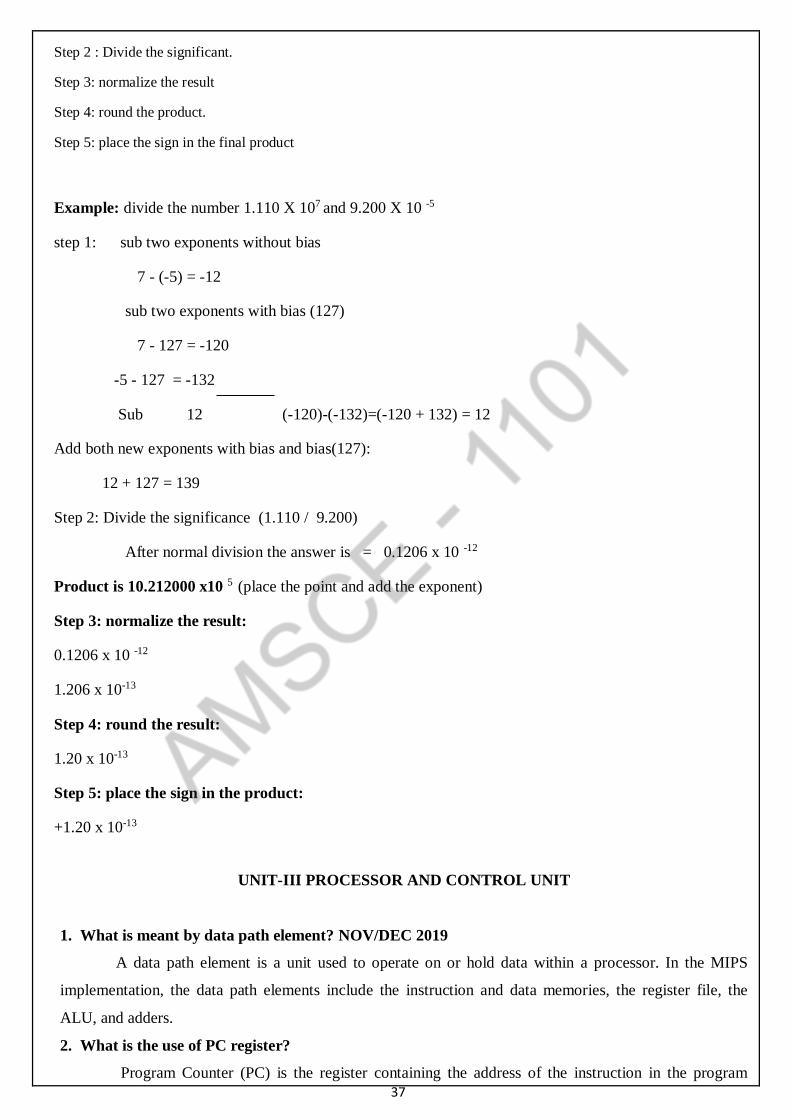
1
CS8491 COMPUTER ARCHITECTURE II YEAR / 4th SEMESTER, CSE
Faculty Name:
DEVI.P.P
Assistant Professor, CSE Department
Aalim Muhammed Salegh College of Engineering
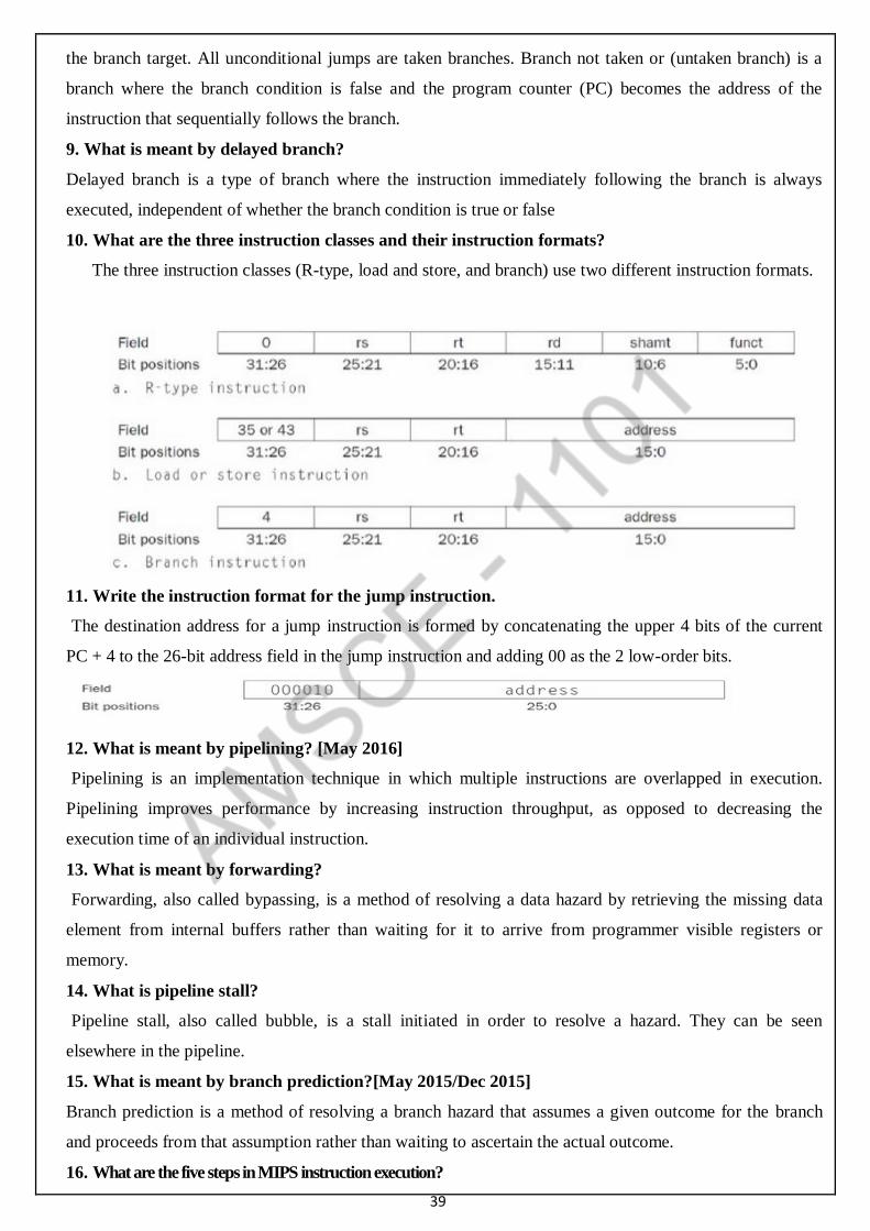
UNIT-I OVERVIEW & INSTRUCTIONS
PART-A
1. What are the five classic components of a computer?APR/MAY 2017
The five classic components of a computer are input, output, memory, datapath, and control, with the last
two sometimes combined and called the processor.
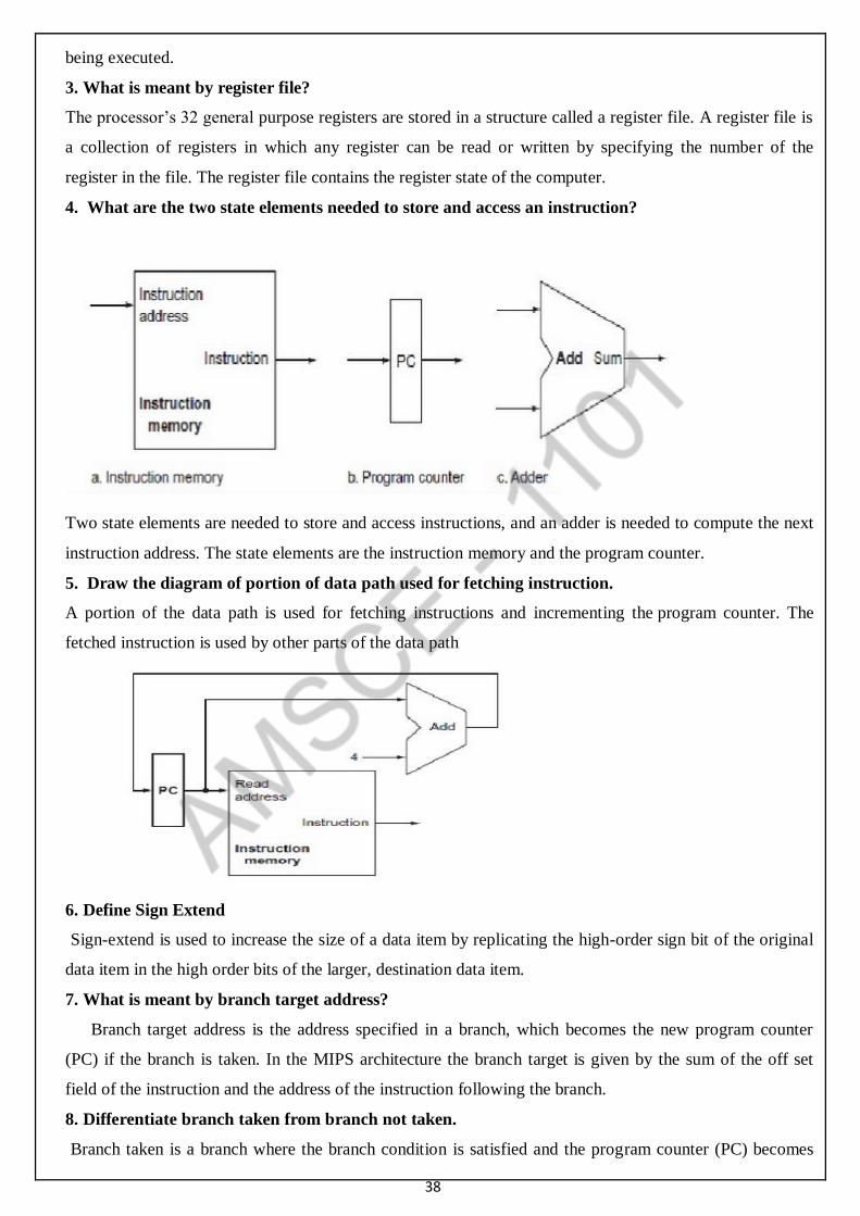
2. Define – Response Time
Response time is also called execution time. The total time required for the computer to complete a task,
including disk accesses, memory accesses, I/O activities, operating system overhead, CPU execution time,
and so on is called response time.
3.Define – Throughput
Throughput or bandwidth is the total amount of work done in a given time.
4. Write the CPU performance equation. APR/MAY 2018
The Classic CPU Performance Equation in terms of instruction count(the number of instructions executed
by the program), CPI, and clock cycle time:
5. If computer A runs a program in 10 seconds, and computer B runs the same program in 15 seconds, how much
faster is A over B.10.
6. What are the basic components of performance?
The basic components of performance and how each is measured are:
Components of Performance Units of measure
2
CPU execution time for a program Seconds for the program
Instruction count Instruction executed for the program
Clock cycles per instruction(CPI) Average number of clock cycles per instruction
Clock cycle time Seconds per clock cycle
7. Write the formula for CPU execution time for a program. [Dec 2015]
8. Write the formula for CPU clock cycles required for a program.
9. Define – MIPS
Million Instructions Per Second (MIPS) is a measurement of program execution speed based on the
number of millions of instructions. MIPS is computed as:
10. What are the fields in an MIPS instruction?
MIPS fields are
Where,
op: Basic operation of the instruction, traditionally called the opcode.
rs: The first register source operand.
rt: The second register source operand.
rd: The register destination operand. It gets the result of the operation.
shamt: Shift amount.
funct: Function.
11. Write an example for immediate operand.
3
The quick add instruction with one constant operand is called add immediate or add i. To add 4 to register
$s3,
we just write
addi $s3,$s3,4 # $s3 = $s3 + 4
12. Define – Stored Program Concepts
Today’s computers are built on two key principles:
1. Instructions are represented as numbers.
2. Programs are stored in memory to be read or written, just like data.
These principles lead to the stored-program concept. Treating instructions in the same way as data greatly
simplifies both the memory hardware and the software of computer systems.
13. How to representing instruction in the computer system [May 2016]
Instructions are kept in computers as a series of high and low electric signals and represented as number.
Each piece of an instruction can be considered as an individual number .
Placing these number side by side forms the instruction.
R- format: register format
I-format: intermediate format
J – format: Jump format
14. Define – Addressing Modes
The different ways in which the operands of an instruction are specified are called as addressing modes.
The MIPS addressing modes are the following:
Register addressing mode
Immediate addressing mode.
Base or displacement addressing mode
Pc-relative addressing mode
Pseudo- direct addressing mode
In direct addressing mode
Auto increment addressing mode
8.Auto decrement addressing mode
15.Define Register mode and Absolute Mode with examples.
Register mode:
The operand is the contents of the processor register. The name (address) of the register is given in the
instruction.
Absolute Mode(Direct Mode):
The operand is in new location. The address of this location is given explicitly in the instruction.
Eg: MOVE LOC,R2
The above instruction uses the register and absolute mode.
The processor register is the temporary storage where the data in the register are accessed using register
4
mode.
The absolute mode can represent global variables in the program.
Mode Assembler Syntax Addressing Function
Register mode Ri EA=Ri
Absolute mode LOC EA=LOC
Where EA-Effective Address
16.What is a Immediate addressing Mode?
The operand is given explicitly in the instruction.
Eg: Move 200 immediate ,R0
It places the value 200 in the register R0.The immediate mode used to specify the value of source operand.
In assembly language, the immediate subscript is not appropriate so # symbol is used. It can be re-written
as
Move #200,R0
Assembly Syntax: Addressing Function
Immediate #value Operand =value
17.Define Indirect addressing Mode.(Nov/Dec2019), APR/MAY 2017
The effective address of the operand is the contents of a register .We denote the indirection by the name of
the register or new address given in the instruction.
Fig: Indirect Mode
Address of an operand (B) is stored into R1 register. If we want this operand, we can get it through register
R1(indirection).
The register or new location that contains the address of an operand is called the pointer.
Mode Assembler Syntax Addressing Function
Indirect Ri , LOC EA=[Ri] or EA=[LOC]
18.Define Index addressing Mode.
The effective address of an operand is generated by adding a constant value to the contents of a register.
The constant value uses either special purpose or general purpose register. We indicate the index mode
symbolically as,
X(Ri) Where X – denotes the constant value contained in the instruction
Ri – It is the name of the register involved.
The Effective Address of the operand is,
EA=X + [Ri]
The index register R1 contains the address of a new location and the value of X defines an offset(also
called a displacement).
5
Eg: Add 20(R1) , R2 (or) EA=>1000+20=1020
Index Mode Assembler Syntax Addressing Function
Index X(Ri) EA=[Ri]+X
Base with Index (Ri,Rj) EA=[Ri]+[Rj]
Base with Index and offset X(Ri,Rj) EA=[Ri]+[Rj] +X
19. What is a Relative Addressing mode? [Dec 2015]
It is same as index mode. The difference is, instead of general purpose register, here we can use program
counter(PC).
Relative Mode:
The Effective Address is determined by the Index mode using the PC in place of the general purpose
register (gpr).
This mode can be used to access the data operand. But its most common use is to specify the target address
in branch instruction. Eg. Branch>0 Loop
It causes the program execution to go to the branch target location. It is identified by the name loop if the
branch condition is satisfied.
Mode Assembler Syntax Addressing Function
Relative X(PC) EA=[PC]+X
20.Define Auto-increment addressing mode. [May 2016]
The Effective Address of the operand is the contents of a register in the instruction.
After accessing the operand, the contents of this register is automatically incremented to point to the next
item in the list.
Mode Assembler syntax Addressing Function
Auto-increment (Ri)+ EA=[Ri]; Increment Ri
21.Define Auto-decrement addressing mode. [May 2016]
The Effective Address of the operand is the contents of a register in the instruction.
After accessing the operand, the contents of this register is automatically decremented to point to the next
item in the list.
Mode Assembler Syntax Addressing Function
Auto-decrement -(Ri) EA=[Ri]; Decrement Ri
PART-B
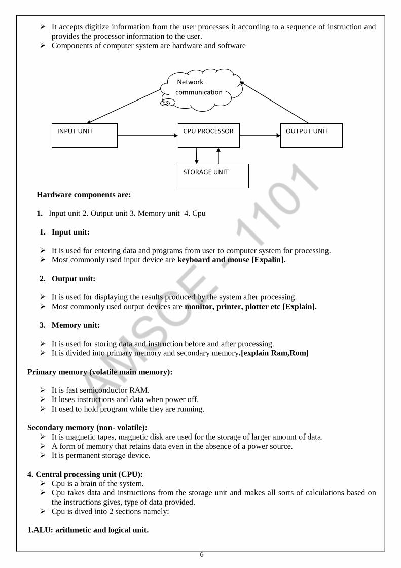
1.Explain in detail the various Components of a computer systems with neat
diagram?
(MAY/ JUNE 2016, NOV/DEC 2015 , NOV/DEC 2014, APR/MAY
2018,APR/MAY 2019, NOV/DEC 2019)
A computer in its simplest form is a fast electronic machine.
6
It accepts digitize information from the user processes it according to a sequence of instruction and
provides the processor information to the user.
Components of computer system are hardware and software
Hardware components are:
1. Input unit 2. Output unit 3. Memory unit 4. Cpu
1. Input unit:
It is used for entering data and programs from user to computer system for processing.
Most commonly used input device are keyboard and mouse [Expalin].
2. Output unit:
It is used for displaying the results produced by the system after processing.
Most commonly used output devices are monitor, printer, plotter etc [Explain].
3. Memory unit:
It is used for storing data and instruction before and after processing.
It is divided into primary memory and secondary memory.[explain Ram,Rom]
Primary memory (volatile main memory):
It is fast semiconductor RAM.
It loses instructions and data when power off.
It used to hold program while they are running.
Secondary memory (non- volatile):
It is magnetic tapes, magnetic disk are used for the storage of larger amount of data.
A form of memory that retains data even in the absence of a power source.
It is permanent storage device.
4. Central processing unit (CPU):
Cpu is a brain of the system.
Cpu takes data and instructions from the storage unit and makes all sorts of calculations based on
the instructions gives, type of data provided.
Cpu is dived into 2 sections namely:
1.ALU: arithmetic and logical unit.
INPUT UNIT CPU PROCESSOR OUTPUT UNIT
STORAGE UNIT
Network
communication
7
All arithmetic and logical operations are performed by the ALU.
To perform these operations operands from the main memory are brought into internal registers of
processor.
After performing operation the result is either stored in the register or memory.
2. Control unit:
It co-ordinates and controls all the activities among the functional units.
A basic function of control unit is to fetch the instructions stored in main memory, identify the
operations and devices involved in it and accordingly generate control signals to execute the desired
operations.
Network communication:
Network have becomes so popular that they are the backbone of current computer systems.
Networked computer have several major advantages:
Communication: Information is exchanged between computers at high speeds.
Resource sharing: Rather than each computer having its own I/O devices, computers on the
network can share I/O devices.
Nonlocal access: By connecting computers over long distances, users need not be near the
computer they are using.
Software components: Software is a collection of progam
Computer software is divided into two broad categories:
1. System software 2.Application software
1. System software:
It is collection of programs which is needed in the creation, preparation and execution of other
program.
System software includes editor, assemblers, linker, loader, compilers, interpreters, debuggers and
operating system
2. Application software:
Allows to perform specific task on a computer using capabilities of computer.
Application software to accomplish a task.
Different application software are needed to perform different tasks.
Operating system:
OS Is a collection of routines that tells the computer what to do uner a variety of conditions.
It is used to control the sharing of and interaction among various computer units as they execute
application programs.
2. What is the need for Addressing in a computer system? Explain the different
addressing modes with suitable examples? MAY/JUNE 2016, APR/MAY 2015,
NOV/DEC 2015, APR/MAY 2017, APR/MAY 2018,APR/MAY 2019,NOV/DEC 2019
Addressing modes are the way of specifying an operand or memory address in an instruction.
The different ways in which the location of an operand is specified in an instruction are called address
modes.
Types of addressing modes:
Register addressing mode
8
Immediate addressing mode.
Base or displacement addressing mode
Pc-relative addressing mode
Pseudo- direct addressing mode
In direct addressing mode
Auto increment addressing mode
Auto decrement addressing mode
Register addressing mode:
Is the considered the simplest addressing mode.
Because the operands are in register.
It allows the instructions to be executed much faster.
It is a form of direct addressing.
Example: add $s0, Ss1, $s2 where s1=5, s2=8
s1(5) s2(8) s0(13)
Register
Immediate Addressing Mode:
MIPS immediate addressing means that one operand is a constant within the instruction itself.
The advantage of using it is that there is no need to have extra memory access to fetch the operand.
But keep in mind that the operand is limited to 16 bits in size.
Example: addi $s0, $s1, 4 s1=5
S1(5) s0(9)
register
memory
Base or displacement addressing mode:
Base address is a data or instruction memory location is specified as a signed offset from a register.
Op rs Rt rd shamt Funct
MEMORY
Op rs Rt 4
ALU
ALU
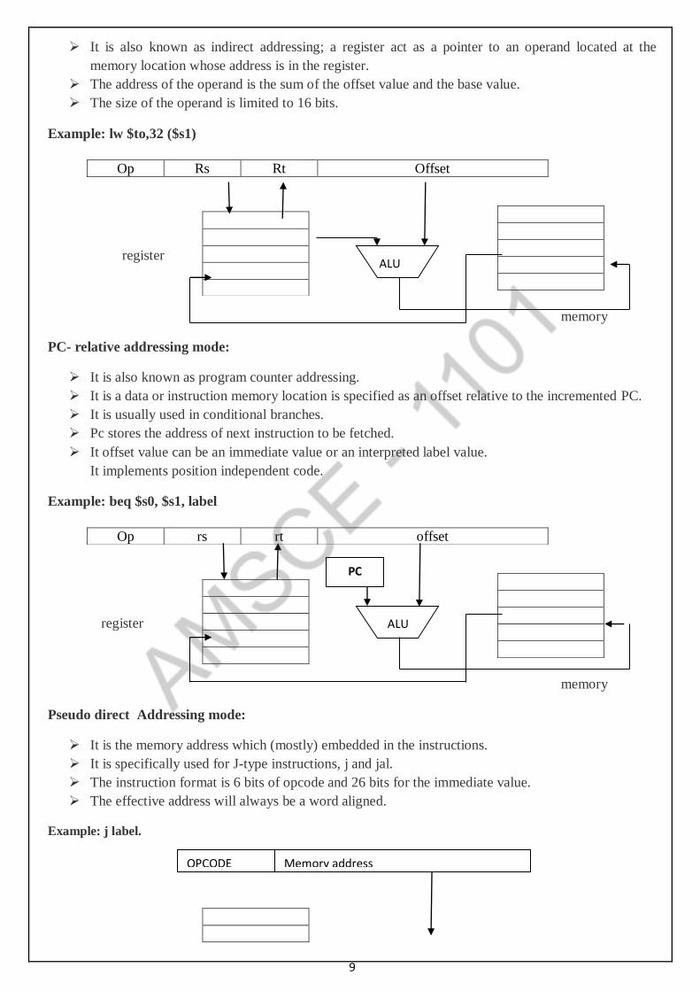
9
It is also known as indirect addressing; a register act as a pointer to an operand located at the
memory location whose address is in the register.
The address of the operand is the sum of the offset value and the base value.
The size of the operand is limited to 16 bits.
Example: lw $to,32 ($s1)
register
memory
PC- relative addressing mode:
It is also known as program counter addressing.
It is a data or instruction memory location is specified as an offset relative to the incremented PC.
It is usually used in conditional branches.
Pc stores the address of next instruction to be fetched.
It offset value can be an immediate value or an interpreted label value.
It implements position independent code.
Example: beq $s0, $s1, label
register
memory
Pseudo direct Addressing mode:
It is the memory address which (mostly) embedded in the instructions.
It is specifically used for J-type instructions, j and jal.
The instruction format is 6 bits of opcode and 26 bits for the immediate value.
The effective address will always be a word aligned.
Example: j label.
Op Rs Rt Offset
Op rs rt offset
ALU
ALU
PC
OPCODE Memory address
10
register
memory
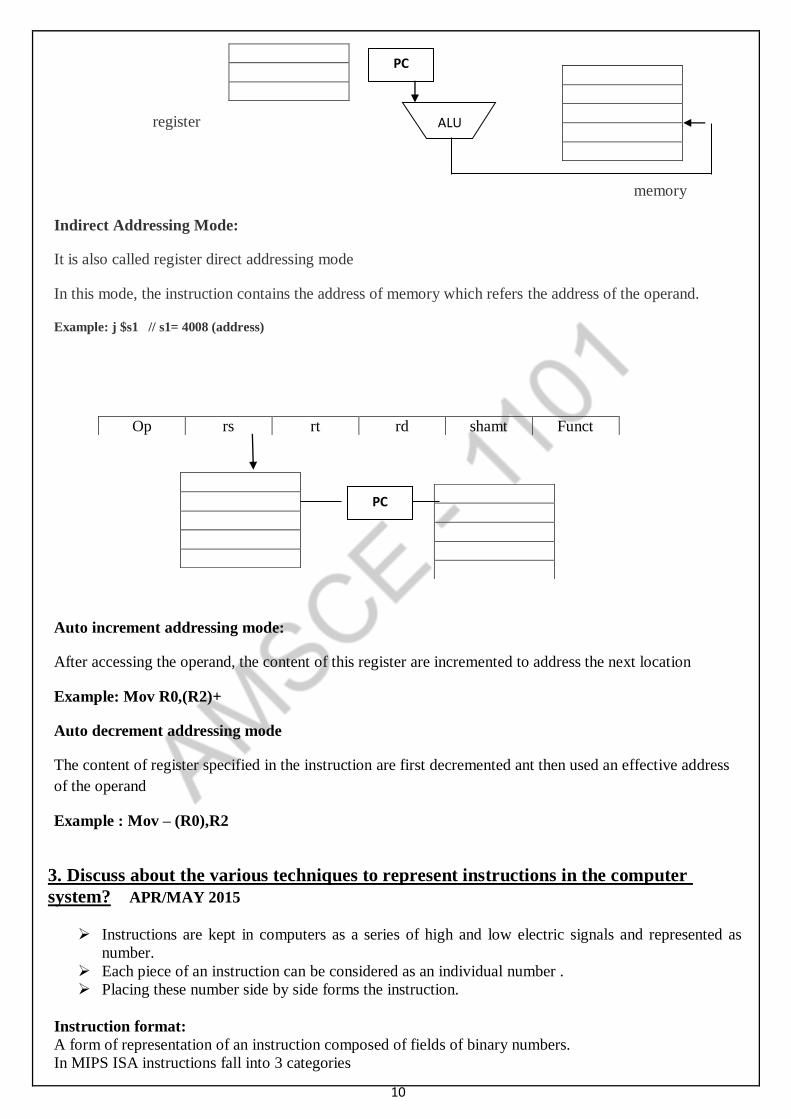
Indirect Addressing Mode:
It is also called register direct addressing mode
In this mode, the instruction contains the address of memory which refers the address of the operand.
Example: j $s1 // s1= 4008 (address)
Auto increment addressing mode:
After accessing the operand, the content of this register are incremented to address the next location
Example: Mov R0,(R2)+
Auto decrement addressing mode
The content of register specified in the instruction are first decremented ant then used an effective address
of the operand
Example : Mov – (R0),R2
3. Discuss about the various techniques to represent instructions in the computer
system? APR/MAY 2015
Instructions are kept in computers as a series of high and low electric signals and represented as
number.
Each piece of an instruction can be considered as an individual number .
Placing these number side by side forms the instruction.
Instruction format:
A form of representation of an instruction composed of fields of binary numbers.
In MIPS ISA instructions fall into 3 categories
Op rs rt rd shamt Funct
PC
ALU
PC
11
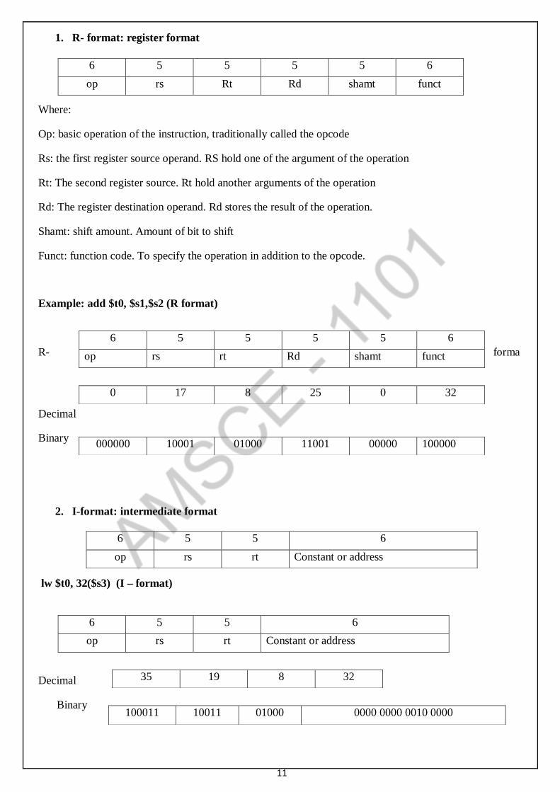
1. R- format: register format
Where:
Op: basic operation of the instruction, traditionally called the opcode
Rs: the first register source operand. RS hold one of the argument of the operation
Rt: The second register source. Rt hold another arguments of the operation
Rd: The register destination operand. Rd stores the result of the operation.
Shamt: shift amount. Amount of bit to shift
Funct: function code. To specify the operation in addition to the opcode.
Example: add $t0, $s1,$s2 (R format)
R- forma
Decimal
Binary
2. I-format: intermediate format
lw $t0, 32($s3) (I – format)
Decimal
Binary
6 5 5 5 5 6
op rs Rt Rd shamt funct
6 5 5 5 5 6
op rs rt Rd shamt funct
0 17 8 25 0 32
000000 10001 01000 11001 00000 100000
6 5 5 6
op rs rt Constant or address
6 5 5 6
op rs rt Constant or address
35 19 8 32
100011 10011 01000 0000 0000 0010 0000
12
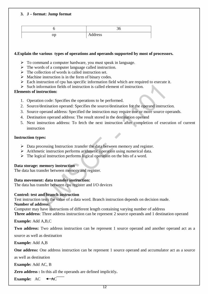
3. J – format: Jump format
4.Explain the various types of operations and operands supported by most of processors.
To command a computer hardware, you must speak in language.
The words of a computer language called instruction.
The collection of words is called instruction set.
Machine instruction is in the form of binary codes.
Each instruction of cpu has specific information field which are required to execute it.
Such information fields of instruction is called element of instruction.
Elements of instruction:
1. Operation code: Specifies the operations to be performed.
2. Source/destination operand: Specifies the source/destination for the operand instruction.
3. Source operand address: Specified the instruction may require one or more source operands.
4. Destination operand address: The result stored in the destination operand
5. Next instruction address: To fetch the next instruction after completion of execution of current
instruction
Instruction types:
Data processing Instruction :transfer the data between memory and register.
Arithmetic instruction performs arithmetic operation using numerical data.
The logical instruction performs logical operation on the bits of a word.
Data storage: memory instruction
The data has transfer between memory and register.
Data movement: data transfer instruction:
The data has transfer between cpu register and I/O devices
Control: test and branch instruction
Test instruction tests the value of a data word. Branch instruction depends on decision made.
Number of address:
Computer may have instructions of different length containing varying number of address
Three address: Three address instruction can be represent 2 source operands and 1 destination operand
Example: Add A,B,C
Two address: Two address instruction can be represent 1 source operand and another operand act as a
source as well as destination
Example: Add A,B
One address: One address instruction can be represent 1 source operand and accumulator act as a source
as well as destination
Example: Add AC, B
Zero address : In this all the operands are defined implicitly.
Example: AC AC
6 36
op Address
13
1. Operations and operand
Operations of computer hardware:
Instructions step by step instructions in a top down fashion.
In MIPS processor (Advance Risk Machine (ARM)) , the declaration is always done by the register.
It support 32 bit register.
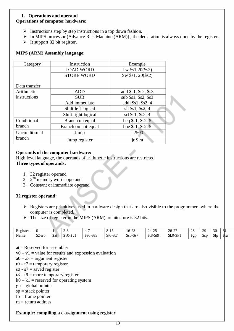
MIPS (ARM) Assembly language:
Category Instruction Example
Data transfer
LOAD WORD Lw $s1,20($s2)
STORE WORD Sw $s1, 20($s2)
Arithmetic
instructions
ADD add $s1, $s2, $s3
SUB sub $s1, $s2, $s3
Add immediate addi $s1, $s2, 4
Shift left logical sll $s1, $s2, 4
Shift right logical srl $s1, $s2, 4
Conditional
branch
Branch on equal beq $s1, $s2, 5
Branch on not equal bne $s1, $s2, 5
Unconditional
branch
Jump j 2500
Jump register jr $ ra
Operands of the computer hardware:
High level language, the operands of arithmetic instructions are restricted.
Three types of operands:
1. 32 register operand
2. 230 memory words operand
3. Constant or immediate operand
32 register operand:
Registers are primitives used in hardware design that are also visible to the programmers where the
computer is completed.
The size of register in the MIPS (ARM) architecture is 32 bits.
at – Reserved for assembler
v0 – v1 = value for results and expression evaluation
a0 – a3 = argument register
t0 – t7 = temporary register
s0 - s7 = saved register
t8 – t9 = more temporary register
k0 – k1 = reserved for operating system
gp = global pointer
sp = stack pointer
fp = frame pointer
ra = return address
Example: compiling a c assignment using register
Register 0 1 2-3 4-7 8-15 16-23 24-25 26-27 28 29 30 31
Name $Zero $at $v0-$v1 $a0-$a3 $t0-$t7 $s0-$s7 $t8-$t9 $k0-$k1 $gp $sp $fp $ra
14
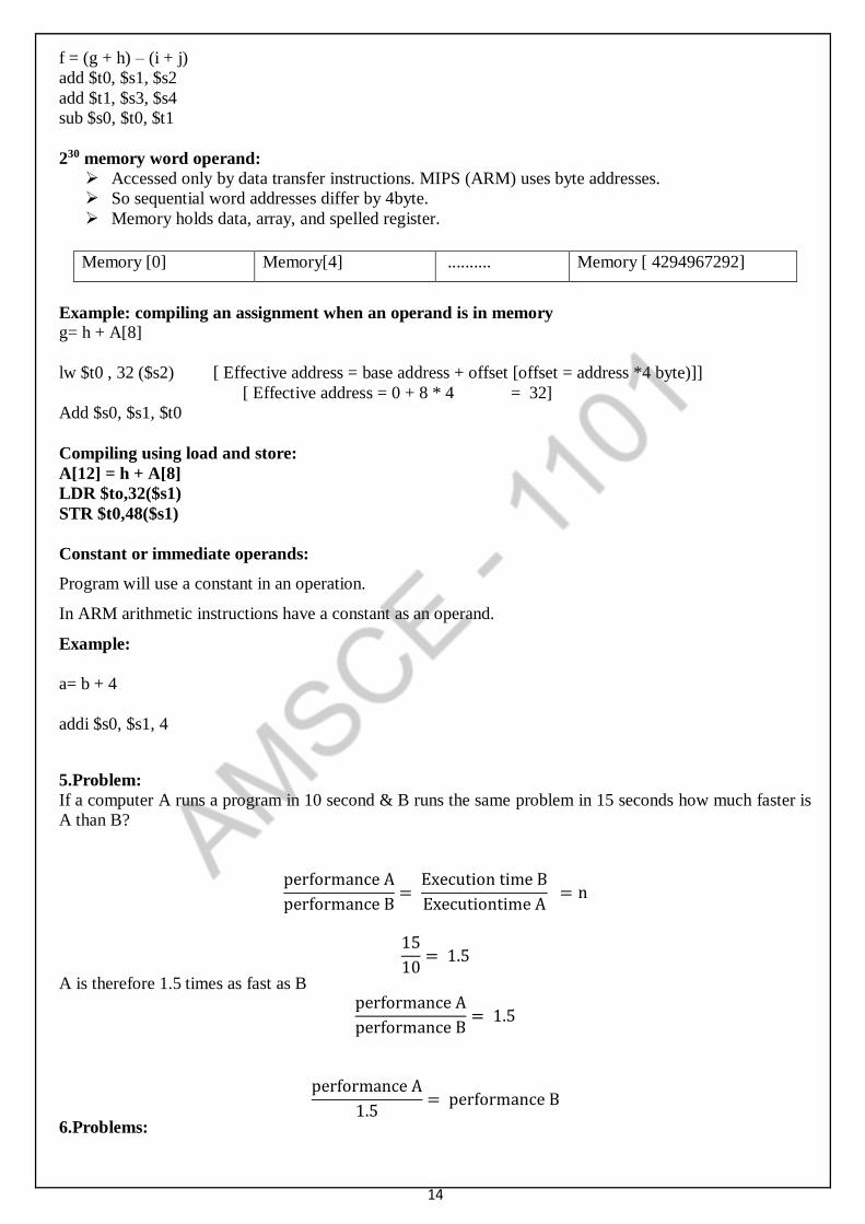
f = (g + h) – (i + j)
add $t0, $s1, $s2
add $t1, $s3, $s4
sub $s0, $t0, $t1
230 memory word operand:
Accessed only by data transfer instructions. MIPS (ARM) uses byte addresses.
So sequential word addresses differ by 4byte.
Memory holds data, array, and spelled register.
Example: compiling an assignment when an operand is in memory
g= h + A[8]
lw $t0 , 32 ($s2) [ Effective address = base address + offset [offset = address *4 byte)]]
[ Effective address = 0 + 8 * 4 = 32]
Add $s0, $s1, $t0
Compiling using load and store:
A[12] = h + A[8]
LDR $to,32($s1)
STR $t0,48($s1)
Constant or immediate operands:
Program will use a constant in an operation.
In ARM arithmetic instructions have a constant as an operand.
Example:
a= b + 4
addi $s0, $s1, 4
5.Problem:
If a computer A runs a program in 10 second & B runs the same problem in 15 seconds how much faster is
A than B?
performance A
performance B=
Execution time B
Executiontime A = n
15
10= 1.5
A is therefore 1.5 times as fast as B performance A
performance B= 1.5
performance A
1.5= performance B
6.Problems:
Memory [0] Memory[4] .......... Memory [ 4294967292]
15
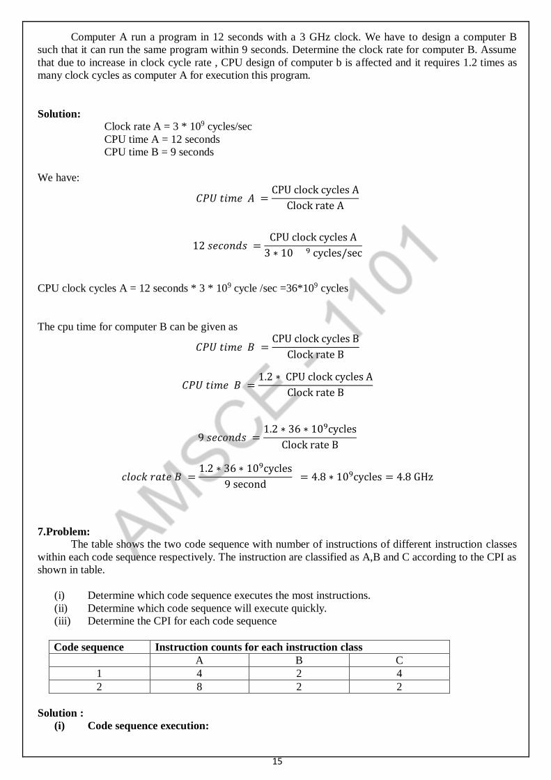
Computer A run a program in 12 seconds with a 3 GHz clock. We have to design a computer B
such that it can run the same program within 9 seconds. Determine the clock rate for computer B. Assume
that due to increase in clock cycle rate , CPU design of computer b is affected and it requires 1.2 times as
many clock cycles as computer A for execution this program.
Solution:
Clock rate A = 3 * 109 cycles/sec
CPU time A = 12 seconds
CPU time B = 9 seconds
We have:
𝐶𝑃𝑈 𝑡𝑖𝑚𝑒 𝐴 =CPU clock cycles A
Clock rate A
12 𝑠𝑒𝑐𝑜𝑛𝑑𝑠 =CPU clock cycles A
3 ∗ 10 9 cycles/sec
CPU clock cycles A = 12 seconds * 3 * 109 cycle /sec =36*109 cycles
The cpu time for computer B can be given as
𝐶𝑃𝑈 𝑡𝑖𝑚𝑒 𝐵 =CPU clock cycles B
Clock rate B
𝐶𝑃𝑈 𝑡𝑖𝑚𝑒 𝐵 =1.2 ∗ CPU clock cycles A
Clock rate B
9 𝑠𝑒𝑐𝑜𝑛𝑑𝑠 =1.2 ∗ 36 ∗ 109cycles
Clock rate B
𝑐𝑙𝑜𝑐𝑘 𝑟𝑎𝑡𝑒 𝐵 =1.2 ∗ 36 ∗ 109cycles
9 second = 4.8 ∗ 109cycles = 4.8 GHz
7.Problem:
The table shows the two code sequence with number of instructions of different instruction classes
within each code sequence respectively. The instruction are classified as A,B and C according to the CPI as
shown in table.
(i) Determine which code sequence executes the most instructions.
(ii) Determine which code sequence will execute quickly.
(iii) Determine the CPI for each code sequence
Code sequence Instruction counts for each instruction class
A B C
1 4 2 4
2 8 2 2
Solution :
(i) Code sequence execution:
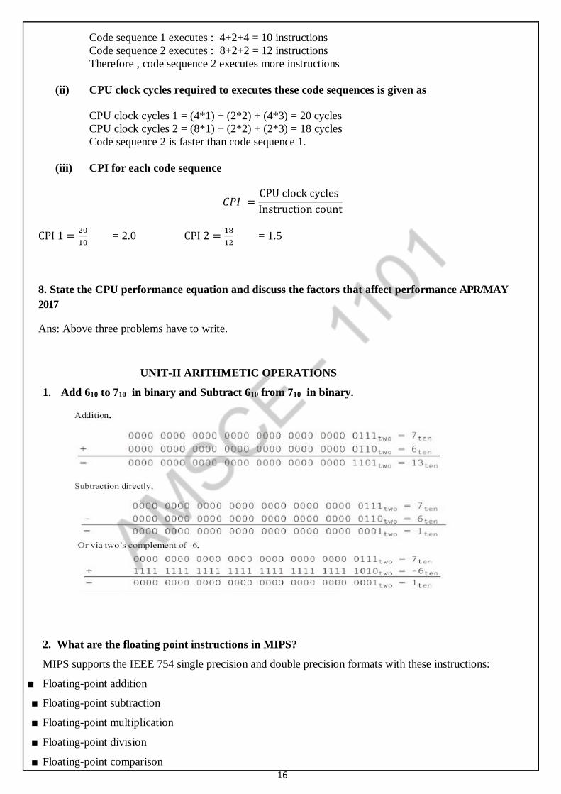
16
Code sequence 1 executes : 4+2+4 = 10 instructions
Code sequence 2 executes : 8+2+2 = 12 instructions
Therefore , code sequence 2 executes more instructions
(ii) CPU clock cycles required to executes these code sequences is given as
CPU clock cycles 1 = (4*1) + (2*2) + (4*3) = 20 cycles
CPU clock cycles 2 = (8*1) + (2*2) + (2*3) = 18 cycles
Code sequence 2 is faster than code sequence 1.
(iii) CPI for each code sequence
𝐶𝑃𝐼 =CPU clock cycles
Instruction count
CPI 1 =20
10 = 2.0 CPI 2 =
18
12 = 1.5
8. State the CPU performance equation and discuss the factors that affect performance APR/MAY
2017
Ans: Above three problems have to write.
UNIT-II ARITHMETIC OPERATIONS
1. Add 610 to 710 in binary and Subtract 610 from 710 in binary.
2. What are the floating point instructions in MIPS?
MIPS supports the IEEE 754 single precision and double precision formats with these instructions:
■ Floating-point addition
■ Floating-point subtraction
■ Floating-point multiplication
■ Floating-point division
■ Floating-point comparison
17
■ Floating-point branch
3. Define Guard and Round
Guard is the first of two extra bits kept on the right during intermediate calculations of floating
point numbers. It is used to improve rounding accuracy.
Round is a method to make the intermediate floating-point result fit the floating-point format; the
goal is typically to find the nearest number that can be represented in the format. IEEE 754, therefore,
always keeps two extra bits on the right during intermediate additions, called guard and round,
respectively.
4. Define ULP
Units in the Last Place is defined as the number of bits in error in the least significant bits of the
significant between the actual number and the number that can be represented.
5. What is meant by sub-word parallelism? [May 2015/May 2016], APR/MAY 2017
Given that the parallelism occurs within a wide word, the extensions are classified as sub-word
parallelism. It is also classified under the more general name of data level parallelism. They have been also
called vector or SIMD, for single instruction, multiple data . The rising popularity of multimedia
applications led to arithmetic instructions that support narrower operations that can easily operate in
parallel.
For example, ARM added more than 100 instructions in the NEON multimedia instruction extension to
support sub-word parallelism, which can be used either withARMv7 or ARMv8.
6. What is meant by sticky bit?
Sticky bit is a bit used in rounding in addition to guard and round that is set when ever there are nonzero
bits to the right of the round bit. This sticky bit allows the computer to see the difference between 0.50 …
00 ten and .... 01 ten when rounding
7. What are the steps in the floating-point addition? APR/MAY 2017
The steps in the floating-point addition are
1. Align the decimal point of the number that has the smaller exponent.
2. Addition of the significands.
3. Normalize the sum.
4. Round the result.
8. Write the IEEE 754 floating point format.
The IEEE 754 standard floating point representation is almost always an approximation of the real number
9.Write the overflow conditions for addition and subtraction [May 2015/Dec 2015]
18
10. Multiply 100010 * 100110.
11. Divide 1,001,010 ten by 1000 ten
12. Define Little Endian arrangement? [Dec 2014]
When lower byte addresses are used for the less significant bytes (rightmost bytes) of the word.
Draw the diagram in notes
13.Define ALU [May 2016]
ALU stands for Arithmetic Logic Unit, ALU is responsible for performing arithmetic operations such
as add, subtract, division and multiplication and logical operation such as AND, OR, Inverting etc.
Arithmetic operation to be performed is based on data type.
Two basic data types:
1. Fixed point numbers
2. Floating point numbers
14.State the representation of double precision of floating point number. [Dec 2015]
The IEEE-754 double precision occupies a two 32 bit words.
63 62 52 51 0
S : sign of number. 0- signifies +ve, 1- signifies –ve
S E’ M
19
E’ : 11 bit signed exponent in excess-1023 representation.
M : 52 bit mantissa fraction
15.what are overflow and underflow condition [Dec 2015]
Overflow:
A situation in which a positive exponent becomes too large to fit in the exponent field.
In single precision , if the number requires an exponent greater than +127
In double precision , if the number requires an exponent greater than +1023
underflow :
A situation in which a negative exponent becomes too large to fi t in the exponent
field.
In single precision , if the number requires an exponent less than -126
In double precision , if the number requires an exponent less than -1022
16. State the principle of operation of a carry look-ahead adder.
The input carry needed by a stage is directly computed from carry signals obtained from all the preceding
stages i-1,i-2,…..0, rather than waiting for normal carries to supply slowly from stage to stage. An adder
that uses this principle is called carry look-ahead adder.
17.What are the main features of Booth’s algorithm? NOV/DEC 2019
It handles both positive and negative multipliers uniformly.
It achieves some efficiency in the number of addition required when the multiplier has a few large blocks
of 1s.
18.How can we speed up the multiplication process?
There are two techniques to speed up the multiplication process:
o The first technique guarantees that the maximum number of summands that must be added is n/2 for n-bit
operands.
o The second technique reduces the time needed to add the summands.
19.What is bit pair recoding? Give an example.
Bit pair recoding halves the maximum number of summands. Group the Booth-recoded multiplier bits in
pairs and observe the following:
The pair (+1 -1) is equivalent to the pair (0 +1). That is instead of adding -1 times the multiplicand m at
shift position i to +1 ( M at position i+1, the same result is obtained by adding +1 ( M at position i.
Eg: 11010 – Bit Pair recoding value is 0 -1 -2
20.What is the advantage of using Booth algorithm?
It handles both positive and negative multiplier uniformly.
20
It achieves efficiency in the number of additions required when the multiplier has a few large blocks of 1’s.
The speed gained by skipping 1’s depends on the data.
21.Write the algorithm for restoring division.
Do the following for n times:
Shift A and Q left one binary position.
Subtract M and A and place the answer back in A.
If the sign of A is 1, set q0 to 0 and add M back to A. Where A- Accumulator, M- Divisor, Q- Dividend.
22.Write the algorithm for non restoring division.
Do the following for n times:
Step 1: Do the following for n times:
If the sign of A is 0 , shift A and Q left one bit position and subtract M from A; otherwise , shift A and Q
left and add M to A.
Now, if the sign of A is 0,set q0 to 1;otherwise , set q0 to0.
Step 2: if the sign of A is 1, add M to A.
23.When can you say that a number is normalized?
When the decimal point is placed to the right of the first (nonzero) significant digit, the number is said to
be normalized.
24. Explain about the special values in floating point numbers.
The end values 0 to 255 of the excess-127 exponent E are used to represent special values such as:
When E= 0 and the mantissa fraction M is zero the value exact 0 is represented. When E= 255 and M=0,
the value is represented.
When E= 0 and M = 0 , denormal values are represented.
When E= 2555 and M =0, the value represented is called Not a number.
25.What is the purpose of guard bits used in floating point arithmetic
Although the mantissa of initial operands are limited to 24 bits, it is important to retain extra bits, called as
guard bits.
26.What are the ways to truncate the guard bits?
There are several ways to truncate the guard bits:
1) Chopping
2) Von Neumann rounding
3) Rounding
27.Define carry save addition(CSA) process.
Instead of letting the carries ripple along the rows, they can be saved and introduced into the next roe at the
21
correct weighted position. Delay in CSA is less than delay through the ripple carry adder.
28.What are generate and propagate function?
The generate function is given by Gi=xiyi and
The propagate function is given as
Pi=xi+yi.
29. What are the difficulties faced when we use floating point arithmetic?
Mantissa overflow: The addition of two mantissas of the same sign may result in a carryout of the most
significant bit
Mantissa underflow: In the process of aligning mantissas ,digits may flow off the right end of the
mantissa.
Exponent overflow: Exponent overflow occurs when a positive exponent exceeds the maximum possible
value.
Exponent underflow: It occurs when a negative exponent exceeds the maximum possible exponent value.
PART-B
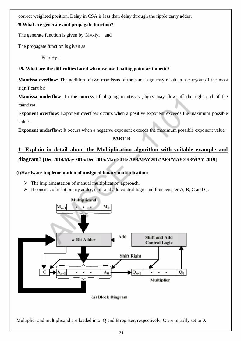
1. Explain in detail about the Multiplication algorithm with suitable example and
diagram? [Dec 2014/May 2015/Dec 2015/May 2016/ APR/MAY 2017/ APR/MAY 2018/MAY 2019]
(i)Hardware implementation of unsigned binary multiplication:
The implementation of manual multiplication approach.
It consists of n-bit binary adder, shift and add control logic and four register A, B, C and Q.
Multiplier and multiplicand are loaded into Q and B register, respectively C are initially set to 0.
22
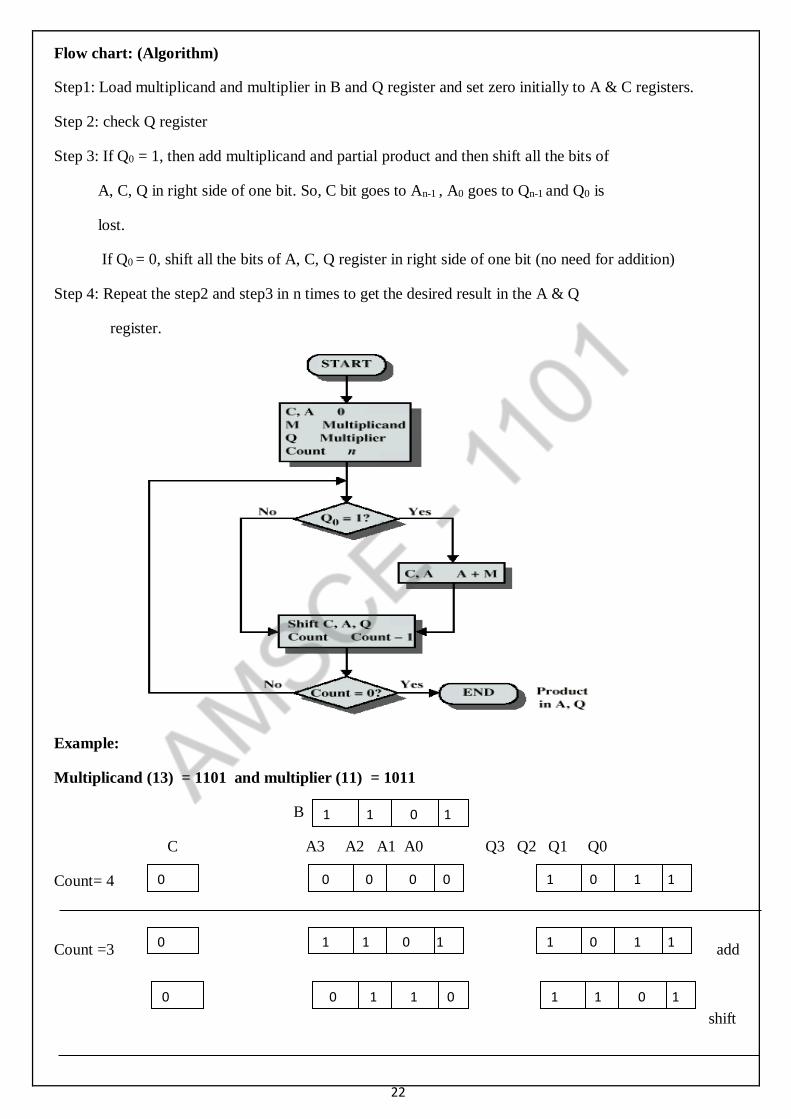
Flow chart: (Algorithm)
Step1: Load multiplicand and multiplier in B and Q register and set zero initially to A & C registers.
Step 2: check Q register
Step 3: If Q0 = 1, then add multiplicand and partial product and then shift all the bits of
A, C, Q in right side of one bit. So, C bit goes to An-1 , A0 goes to Qn-1 and Q0 is
lost.
If Q0 = 0, shift all the bits of A, C, Q register in right side of one bit (no need for addition)
Step 4: Repeat the step2 and step3 in n times to get the desired result in the A & Q
register.
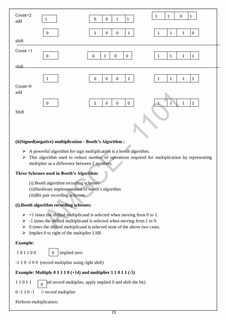
Example:
Multiplicand (13) = 1101 and multiplier (11) = 1011
B
C A3 A2 A1 A0 Q3 Q2 Q1 Q0
Count= 4
Count =3 add
shift
0
1 1 0 1
0 0 0 0 1 0 1 1
0 1 1 0 1 1 0 1 1
0 0 1 1 0 1 1 0 1
23
Count=2
add
shift
Count =1
shift
Count=0
add
Shift
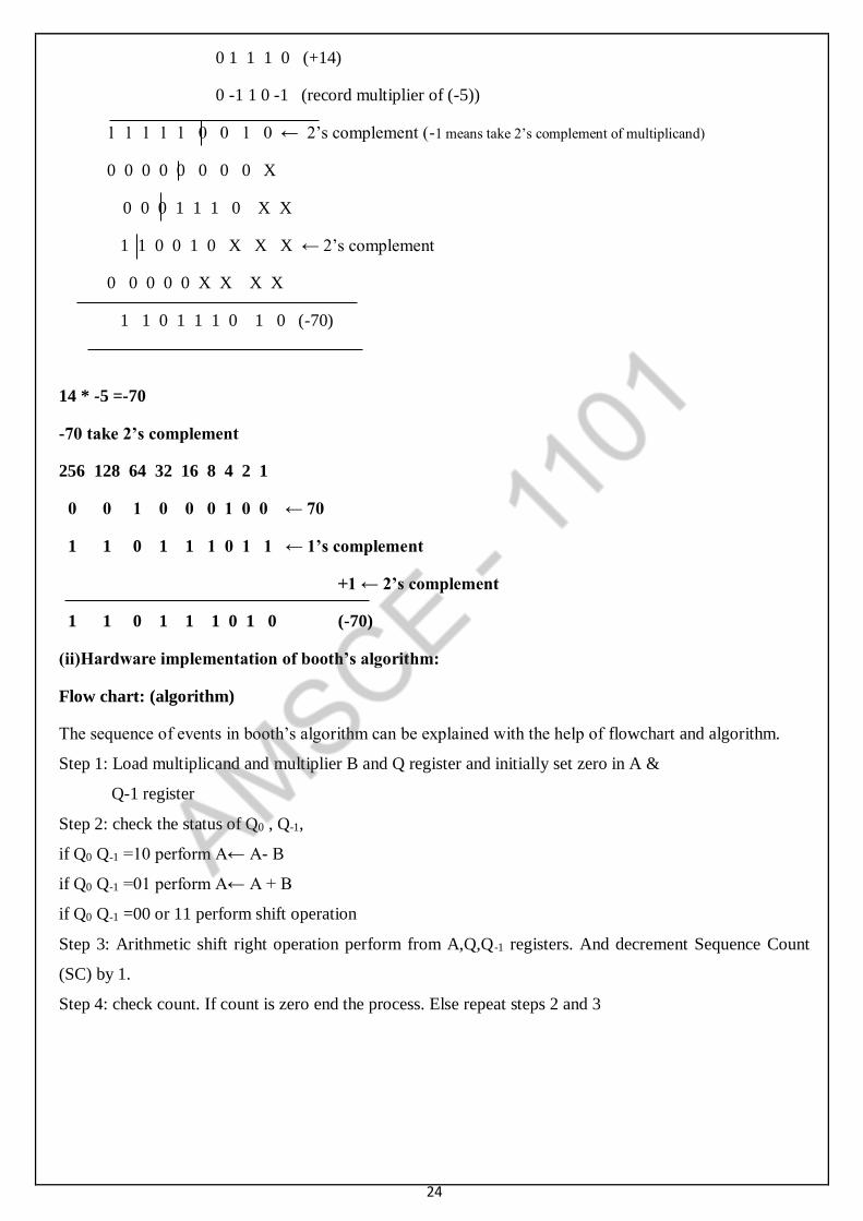
(ii)Signed(negative) multiplication - Booth’s Algorithm :
A powerful algorithm for sign multiplication is a booth algorithm.
This algorithm used to reduce number of operations required for multiplication by representing
multiplier as a difference between 2 numbers.
Three Schemes used in Booth’s Algorithm:
(i).Booth algorithm recording schemes
(ii)Hardware implementation of booth’s algorithm
(iii)Bit pair recording schemes
(i).Booth algorithm recording schemes:
+1 times the shifted multiplicand is selected when moving from 0 to 1.
-1 times the shifted multiplicand is selected when moving from 1 to 0.
0 times the shifted multiplicand is selected none of the above two cases.
Implies 0 to right of the multiplier LSB.
Example:
1 0 1 1 0 0 implied zero
-1 1 0 -1 0 0 (record multiplier using right shift)
Example: Multiply 0 1 1 1 0 (+14) and multiplier 1 1 0 1 1 (-5)
1 1 0 1 1 (find record multiplier, apply implied 0 and shift the bit)
0 -1 1 0 -1 // record multiplier
Perform multiplication:
1 0 0 1 1 1 1 0 1
0 1 0 0 1 1 1 1 0
0
0 1 0 0 1 1 1 1
1 0 0 0 1 1 1 1 1
0 1 0 0 0 1 1 1 1
0
0
24
0 1 1 1 0 (+14)
0 -1 1 0 -1 (record multiplier of (-5))
1 1 1 1 1 0 0 1 0 ← 2’s complement (-1 means take 2’s complement of multiplicand)
0 0 0 0 0 0 0 0 X
0 0 0 1 1 1 0 X X
1 1 0 0 1 0 X X X ← 2’s complement
0 0 0 0 0 X X X X
1 1 0 1 1 1 0 1 0 (-70)
14 * -5 =-70
-70 take 2’s complement
256 128 64 32 16 8 4 2 1
0 0 1 0 0 0 1 0 0 ← 70
1 1 0 1 1 1 0 1 1 ← 1’s complement
+1 ← 2’s complement
1 1 0 1 1 1 0 1 0 (-70)
(ii)Hardware implementation of booth’s algorithm:
Flow chart: (algorithm)
The sequence of events in booth’s algorithm can be explained with the help of flowchart and algorithm.
Step 1: Load multiplicand and multiplier B and Q register and initially set zero in A &
Q-1 register
Step 2: check the status of Q0 , Q-1,
if Q0 Q-1 =10 perform A← A- B
if Q0 Q-1 =01 perform A← A + B
if Q0 Q-1 =00 or 11 perform shift operation
Step 3: Arithmetic shift right operation perform from A,Q,Q-1 registers. And decrement Sequence Count
(SC) by 1.
Step 4: check count. If count is zero end the process. Else repeat steps 2 and 3
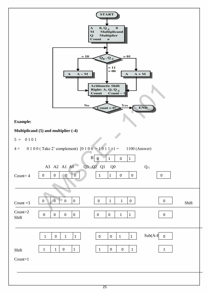
25
Example:
Multiplicand (5) and multiplier (-4)
5 = 0 1 0 1
4 = 0 1 0 0 ( Take 2’ complement) [0 1 0 0 = 1 0 1 1 +1 = 1100 (Answer)
B
A3 A2 A1 A0 Q3 Q2 Q1 Q0 Q-1
Count= 4
Count =3 Shift
Count=2
Shift
Sub(A-B)
Shift
Count=1
0
0 1 0 1
0 0 0 0 1 1 0 0
0 0 0 0 0 0 1 1 0
0 0 0 0 0 0 0 1 1
0 1 0 1 1 0 0 1 1
1 1 1 0 1 1 0 0 1
26
Count = 0
Shift
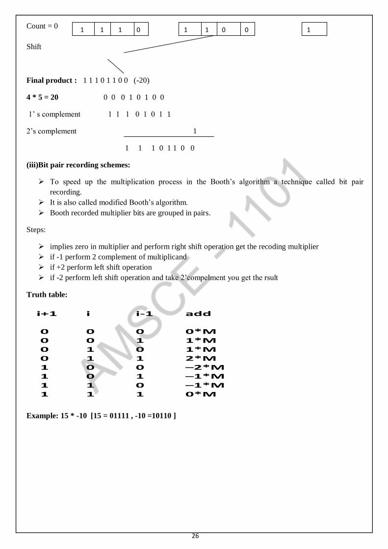
Final product : 1 1 1 0 1 1 0 0 (-20)
4 * 5 = 20 0 0 0 1 0 1 0 0
1’ s complement 1 1 1 0 1 0 1 1
2’s complement 1
1 1 1 0 1 1 0 0
(iii)Bit pair recording schemes:
To speed up the multiplication process in the Booth’s algorithm a technique called bit pair
recording.
It is also called modified Booth’s algorithm.
Booth recorded multiplier bits are grouped in pairs.
Steps:
implies zero in multiplier and perform right shift operation get the recoding multiplier
if -1 perform 2 complement of multiplicand
if +2 perform left shift operation
if -2 perform left shift operation and take 2’compelment you get the rsult
Truth table:
Example: 15 * -10 [15 = 01111 , -10 =10110 ]
1
1 1 1 0 1 1 0 0
27
0 1 1 1 1 (+15)
-1 +2 -2 (record multiplier of (-10))
1 1 1 1 1 0 0 0 1 0 ←(-2 : left shift and take 2’s complement of multiplicand)
0 0 0 1 1 1 1 0 X X ←( +2 : left shift of multiplicand)
1 1 0 0 0 1 X X X X ←( -1 : 2’s complement)
1 1 0 1 1 0 1 0 1 0 (-150)
Note: Any one algorithm you can write either positive or negative
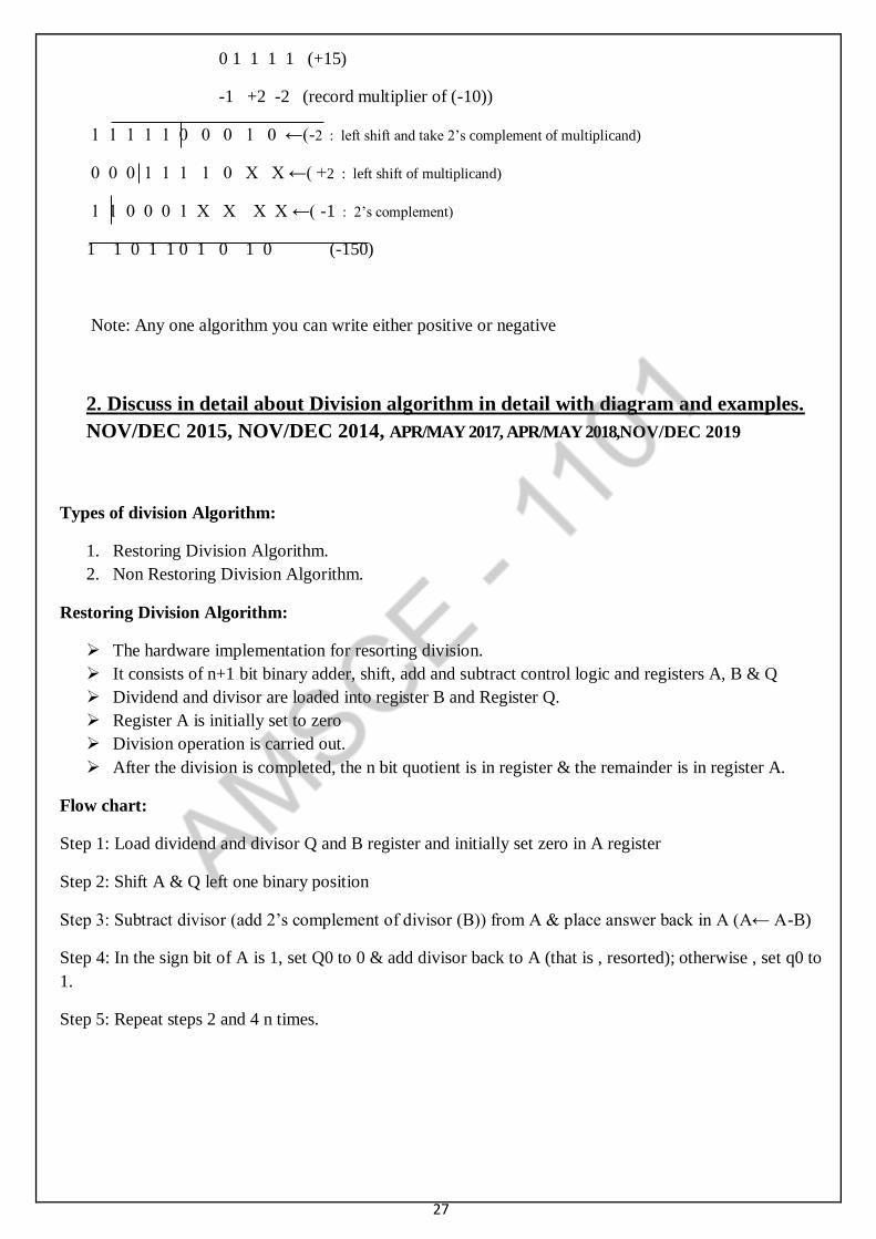
2. Discuss in detail about Division algorithm in detail with diagram and examples.
NOV/DEC 2015, NOV/DEC 2014, APR/MAY 2017, APR/MAY 2018,NOV/DEC 2019
Types of division Algorithm:
1. Restoring Division Algorithm.
2. Non Restoring Division Algorithm.
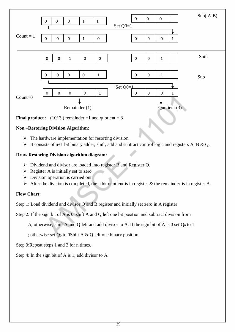
Restoring Division Algorithm:
The hardware implementation for resorting division.
It consists of n+1 bit binary adder, shift, add and subtract control logic and registers A, B & Q
Dividend and divisor are loaded into register B and Register Q.
Register A is initially set to zero
Division operation is carried out.
After the division is completed, the n bit quotient is in register & the remainder is in register A.
Flow chart:
Step 1: Load dividend and divisor Q and B register and initially set zero in A register
Step 2: Shift A & Q left one binary position
Step 3: Subtract divisor (add 2’s complement of divisor (B)) from A & place answer back in A (A← A-B)
Step 4: In the sign bit of A is 1, set Q0 to 0 & add divisor back to A (that is , resorted); otherwise , set q0 to
1.
Step 5: Repeat steps 2 and 4 n times.
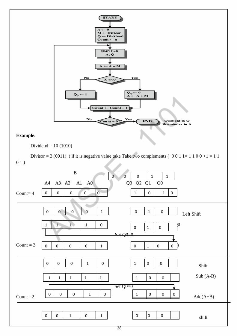
28
Example:
Dividend = 10 (1010)
Divisor = 3 (0011) ( if it is negative value take Take two complements ( 0 0 1 1= 1 1 0 0 +1 = 1 1
0 1 )
B
A4 A3 A2 A1 A0 Q3 Q2 Q1 Q0
Count= 4
Left Shift
Sub(A-B) set Q0
Set Q0=0
Count = 3 Add( A+B)
Shift
Sub (A-B)
Set Q0=0
Count =2 Add(A+B)
shift
1 0 1 0
0 1 0
0 1 0
0 1 0 0
1 0 0
0 0 0 1 1
0 0 0 0 0
0 0 0 0 1
1 1 1 1 0
0 0 0 0 1
0 0 0 1 0
1 1 1 1 1 1 0 0
1 0 0 0 0 0 0 1 0
0 0 1 0 1 0 0 0
1 0 0 0
29
Sub( A-B)
Set Q0=1
Count = 1
Shift
Sub
Set Q0=1
Count=0
Remainder (1) Quotient (3)
Final product : (10/ 3 ) remainder =1 and quotient = 3
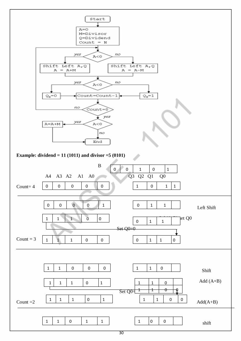
Non –Restoring Division Algorithm:
The hardware implementation for resorting division.
It consists of n+1 bit binary adder, shift, add and subtract control logic and registers A, B & Q.
Draw Restoring Division algorithm diagram:
Dividend and divisor are loaded into register B and Register Q.
Register A is initially set to zero
Division operation is carried out.
After the division is completed, the n bit quotient is in register & the remainder is in register A.
Flow Chart:
Step 1: Load dividend and divisor Q and B register and initially set zero in A register
Step 2: If the sign bit of A is 0, shift A and Q left one bit position and subtract division from
A; otherwise, shift A and Q left and add divisor to A. If the sign bit of A is 0 set Q0 to 1
; otherwise set Q0 to 0Shift A & Q left one binary position
Step 3:Repeat steps 1 and 2 for n times.
Step 4: In the sign bit of A is 1, add divisor to A.
0 0 0
0 0 0 1
0 0 0 1 1
0 0 0 1 0
0 0 1 0 0 0 0 1
0 0 1
0 0 0 1
0 0 0 0 1
0 0 0 0 1
30
Example: dividend = 11 (1011) and divisor =5 (0101)
B
A4 A3 A2 A1 A0 Q3 Q2 Q1 Q0
Count= 4
Left Shift
Sub(A-B) set Q0
Set Q0=0
Count = 3
Shift
Add (A+B)
Set Q0=0
Count =2 Add(A+B)
shift
1 0 1 1
0 1 1
0 1 1
0 1 1 0
1 1 0
0 0 1 0 1
0 0 0 0 0
0 0 0 0 1
1 1 1 0 0
1 1 1 0 0
1 1 0 0 0
1 1 1 0 1 1 1 0
1 1 0 0
1 1 1 0 1
1 1 0 1 1 1 0 0
1 1 0 0
31
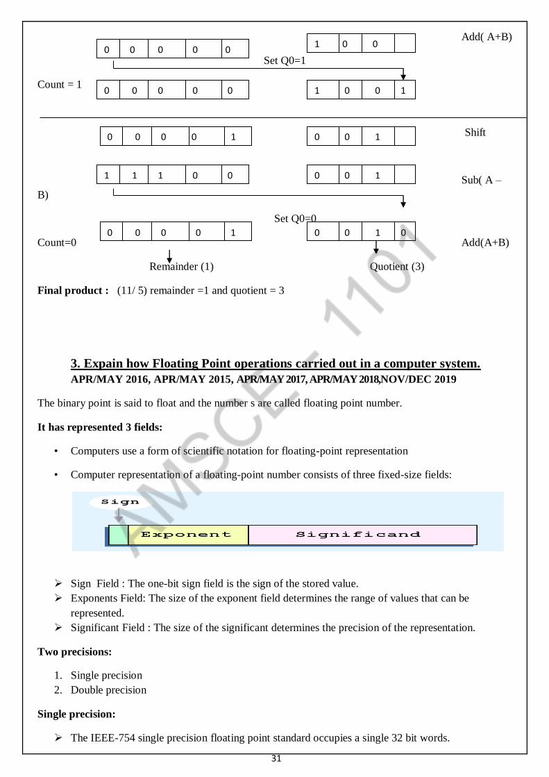
Add( A+B)
Set Q0=1
Count = 1
Shift
Sub( A –
B)
Set Q0=0
Count=0 Add(A+B)
Remainder (1) Quotient (3)
Final product : (11/ 5) remainder =1 and quotient = 3
3. Expain how Floating Point operations carried out in a computer system.
APR/MAY 2016, APR/MAY 2015, APR/MAY 2017, APR/MAY 2018,NOV/DEC 2019
The binary point is said to float and the number s are called floating point number.
It has represented 3 fields:
• Computers use a form of scientific notation for floating-point representation
• Computer representation of a floating-point number consists of three fixed-size fields:
Sign Field : The one-bit sign field is the sign of the stored value.
Exponents Field: The size of the exponent field determines the range of values that can be
represented.
Significant Field : The size of the significant determines the precision of the representation.
Two precisions:
1. Single precision
2. Double precision
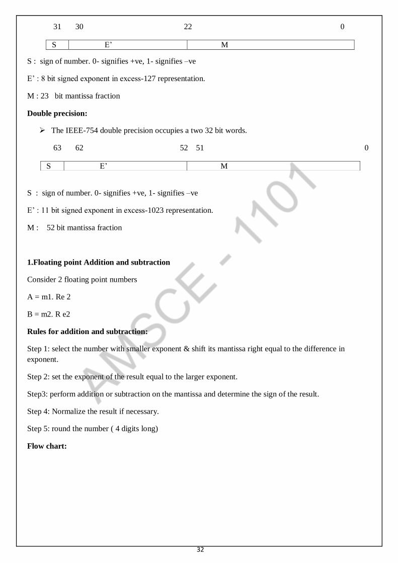
Single precision:
The IEEE-754 single precision floating point standard occupies a single 32 bit words.
1 0 0
1 0 0 1
0 0 0 0 0
0 0 0 0 0
0 0 0 0 1 0 0 1
0 0 1
0 0 1 0
1 1 1 0 0
0 0 0 0 1
32
31 30 22 0
S : sign of number. 0- signifies +ve, 1- signifies –ve
E’ : 8 bit signed exponent in excess-127 representation.
M : 23 bit mantissa fraction
Double precision:
The IEEE-754 double precision occupies a two 32 bit words.
63 62 52 51 0
S : sign of number. 0- signifies +ve, 1- signifies –ve
E’ : 11 bit signed exponent in excess-1023 representation.
M : 52 bit mantissa fraction
1.Floating point Addition and subtraction
Consider 2 floating point numbers
A = m1. Re 2
B = m2. R e2
Rules for addition and subtraction:
Step 1: select the number with smaller exponent & shift its mantissa right equal to the difference in
exponent.
Step 2: set the exponent of the result equal to the larger exponent.
Step3: perform addition or subtraction on the mantissa and determine the sign of the result.
Step 4: Normalize the result if necessary.
Step 5: round the number ( 4 digits long)
Flow chart:
S E’ M
S E’ M
33
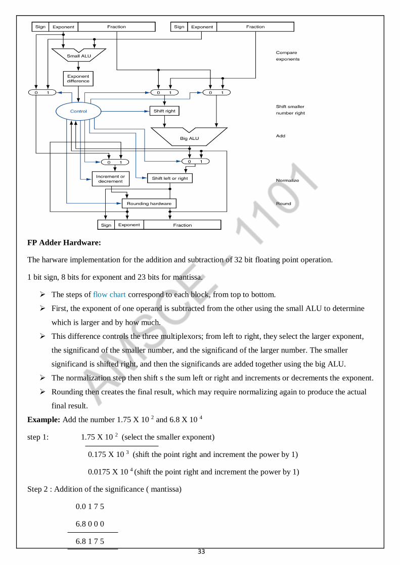
FP Adder Hardware:
The harware implementation for the addition and subtraction of 32 bit floating point operation.
1 bit sign, 8 bits for exponent and 23 bits for mantissa.
The steps of flow chart correspond to each block, from top to bottom.
First, the exponent of one operand is subtracted from the other using the small ALU to determine
which is larger and by how much.
This difference controls the three multiplexors; from left to right, they select the larger exponent,
the significand of the smaller number, and the significand of the larger number. The smaller
significand is shifted right, and then the significands are added together using the big ALU.
The normalization step then shift s the sum left or right and increments or decrements the exponent.
Rounding then creates the final result, which may require normalizing again to produce the actual
final result.
Example: Add the number 1.75 X 10 2 and 6.8 X 10 4
step 1: 1.75 X 10 2 (select the smaller exponent)
0.175 X 10 3 (shift the point right and increment the power by 1)
0.0175 X 10 4 (shift the point right and increment the power by 1)
Step 2 : Addition of the significance ( mantissa)
0.0 1 7 5
6.8 0 0 0
6.8 1 7 5
34
Step 3: Normalize the result
6.8 1 7 5 X 10 4
Step 4: round of the sum
6.8 1 8 X 10 4
Example: Subtract the number 0.5 ten and -0.4375 ten
Convert decimal to binary first:
0.5 X 2 = 1.0
0.1 X 2 0 (shift the point left and decrement the power by 1)
1.0 X 2 -1 // normalization
0.4375 X 2 = .8750
0.875 X 2 = .750
0.75 X 2 = .50
0.5 X 2 = .0
- 0. 0111 x 2 0 (shift the point left and decrement the power by 1)
- 1.11 X 2 -2 // normalization
step 1: - 1.110 X 2 -2 (select the smaller exponent)
- 0.111 X 2 -1 (shift the point right and increment the power by 1)
Step 2 : Addition of the significant ( mantissa)
1.000 X 2 -1 // normalization
- 0.111 X 2 -1 // take 2’ complement answer // 1.001)
Add the number:
1.000 X 2 -1
1.001 X 2 -1
1 0.001 X 2 -1 [discard the carry)
Step 3: Normalize the result
0.001 X 2 -1 (shift the point left and decrement the power by 1)
00.01 X 2 -2 (shift the point left and decrement the power by 1)
000.1 X 2 -3
1.00 X 2 -4
Step 4: round of the sum: 1.00 X 2 -4
0
1
1
1
35
2.Floating point multiplication:
Rules for Multiplication:
Step 1: Adding the exponent without bias and with bias. And subtract new exponents with bias and bias(127)
Step 2 : multiplication of significant. Step 3: normalize the result
Step 4: round the product.
Step 5: place the sign in the final product
Example: multiply the number 1.110 X 10¹⁰ and 9.200 X 10 -5
step 1: Add two exponents without bias
10 + (-5) = 5
Add two exponents with bias (127)
10 + 127 = 137
-5 + 127 = 122
Add 259
Subtract both new exponents with bias and bias(127):
259 – 127 = 132
Step 2: Multiply the significance (1.110 * 9.200)
1110
9200
0000
0000x
2220xx
9990xxx
10212000
Product is 10.212000 x10 5 (place the point and add the exponent)
Step 3: normalize the result:
10.212000 x 10 5
1.0212000 x 10 6
Step 4: round the result:
1.0212 x 10 6
Step 5: place the sign in the product:
+ 1.0212 x 10 6
Example: multiply the number 0.5 ten and -0.4375 ten
36
Convert decimal to binary first:
0.5 X 2 = 1.0
0.1 X 2 0 (shift the point left and decrement the power by 1)
1.0 X 2 -1 // normalization
0.4375 X 2 = .8750
0.875 X 2 = .750
0.75 X 2 = .50
0.5 X 2 = .0
- 0. 0111 X 2 0 (shift the point left and decrement the power by 1)
- 1.11 X 2 -2 // normalization
step 1: Add two exponents without bias
-1 + (-2) = - 3
Add two exponents with bias (127)
-1 + 127 = 126
-2 + 127 = 125
Add 251
Subtract both new exponents with bias and bias(127):
251 – 127 = 124
Step 2: Multiply the significance (1.0 * 1.11)
1.11
10
1.110
Product is 1.110 x10 -3 (place the point and add the exponent)
Step 3: normalize the result:
1.110 x10 -3
Step 4: round the result:
1.110 x10 -3
Step 5: place the sign in the product:
- 1.110 x10 -3
3.Floating point Division:
Step 1: Subtract the exponent without bias and with bias. And add new exponents with bias and bias (127)
0
1
1
1
37
Step 2 : Divide the significant.
Step 3: normalize the result
Step 4: round the product.
Step 5: place the sign in the final product
Example: divide the number 1.110 X 10⁷ and 9.200 X 10 -5
step 1: sub two exponents without bias
7 - (-5) = -12
sub two exponents with bias (127)
7 - 127 = -120
-5 - 127 = -132
Sub 12 (-120)-(-132)=(-120 + 132) = 12
Add both new exponents with bias and bias(127):
12 + 127 = 139
Step 2: Divide the significance (1.110 / 9.200)
After normal division the answer is = 0.1206 x 10 -12
Product is 10.212000 x10 5 (place the point and add the exponent)
Step 3: normalize the result:
0.1206 x 10 -12
1.206 x 10⁻¹³
Step 4: round the result:
1.20 x 10⁻¹³
Step 5: place the sign in the product:
+1.20 x 10⁻¹³
UNIT-III PROCESSOR AND CONTROL UNIT
1. What is meant by data path element? NOV/DEC 2019
A data path element is a unit used to operate on or hold data within a processor. In the MIPS
implementation, the data path elements include the instruction and data memories, the register file, the
ALU, and adders.
2. What is the use of PC register?
Program Counter (PC) is the register containing the address of the instruction in the program
38
being executed.
3. What is meant by register file?
The processor’s 32 general purpose registers are stored in a structure called a register file. A register file is
a collection of registers in which any register can be read or written by specifying the number of the
register in the file. The register file contains the register state of the computer.
4. What are the two state elements needed to store and access an instruction?
Two state elements are needed to store and access instructions, and an adder is needed to compute the next
instruction address. The state elements are the instruction memory and the program counter.
5. Draw the diagram of portion of data path used for fetching instruction.
A portion of the data path is used for fetching instructions and incrementing the program counter. The
fetched instruction is used by other parts of the data path
6. Define Sign Extend
Sign-extend is used to increase the size of a data item by replicating the high-order sign bit of the original
data item in the high order bits of the larger, destination data item.
7. What is meant by branch target address?
Branch target address is the address specified in a branch, which becomes the new program counter
(PC) if the branch is taken. In the MIPS architecture the branch target is given by the sum of the off set
field of the instruction and the address of the instruction following the branch.
8. Differentiate branch taken from branch not taken.
Branch taken is a branch where the branch condition is satisfied and the program counter (PC) becomes
39
the branch target. All unconditional jumps are taken branches. Branch not taken or (untaken branch) is a
branch where the branch condition is false and the program counter (PC) becomes the address of the
instruction that sequentially follows the branch.
9. What is meant by delayed branch?
Delayed branch is a type of branch where the instruction immediately following the branch is always
executed, independent of whether the branch condition is true or false
10. What are the three instruction classes and their instruction formats?
The three instruction classes (R-type, load and store, and branch) use two different instruction formats.
11. Write the instruction format for the jump instruction.
The destination address for a jump instruction is formed by concatenating the upper 4 bits of the current
PC + 4 to the 26-bit address field in the jump instruction and adding 00 as the 2 low-order bits.
12. What is meant by pipelining? [May 2016]
Pipelining is an implementation technique in which multiple instructions are overlapped in execution.
Pipelining improves performance by increasing instruction throughput, as opposed to decreasing the
execution time of an individual instruction.
13. What is meant by forwarding?
Forwarding, also called bypassing, is a method of resolving a data hazard by retrieving the missing data
element from internal buffers rather than waiting for it to arrive from programmer visible registers or
memory.
14. What is pipeline stall?
Pipeline stall, also called bubble, is a stall initiated in order to resolve a hazard. They can be seen
elsewhere in the pipeline.
15. What is meant by branch prediction?[May 2015/Dec 2015]
Branch prediction is a method of resolving a branch hazard that assumes a given outcome for the branch
and proceeds from that assumption rather than waiting to ascertain the actual outcome.
16. What are the five steps in MIPS instruction execution?
40
1. Fetch instruction from memory.
2. Read registers while decoding the instruction. The regular format of MIPS instructions allows reading
and decoding to occur simultaneously.
3. Execute the operation or calculate an address.
4. Access an operand in data memory.
5. Write the result into a register.
17. Write the formula for calculating time between instructions in a pipelined processor?
18. What are hazards? Write its types. [Dec 2015]
There are situations in pipelining when the next instruction cannot be executed in the following clock
cycle. These events are called hazards, and there are three different types.
1. Structural Hazards
2. Data Hazards
3 . Control Hazards
19. What are the 5 pipeline stages?
The 5 stages of instruction execution in a pipelined processor are:
1. IF: Instruction fetch
2. ID: Instruction decode and register file read
3. EX: Execution or address calculation
4. MEM: Data memory access
5. WB: Write back
20. What are exceptions and interrupts?[Dec 2014/ May 2016]
Exception, also called interrupt, is an unscheduled event that disrupts program execution used to detect
overflow. Eg. Arithmetic overflow, using an undefined instruction. Interrupt is an exception that comes
from outside of the processor.Eg. I/O device request
21. Define – Vectored Interrupts
Vectored interrupt is an interrupt in that the address to which the control is transferred is determined by the
cause of the exception
PART-B
1.Explain the basic MIPS implementation of instruction set
NOV/DEC 2015, APR/MAY 2015, APR/MAY 2019( 16 MARKS )
BASIC MIPS IMPLEMENTATION:
The basic MIPs implementation includes a subset of the core MIPS instruction set.
Every instructions are divided into 3 instruction classes
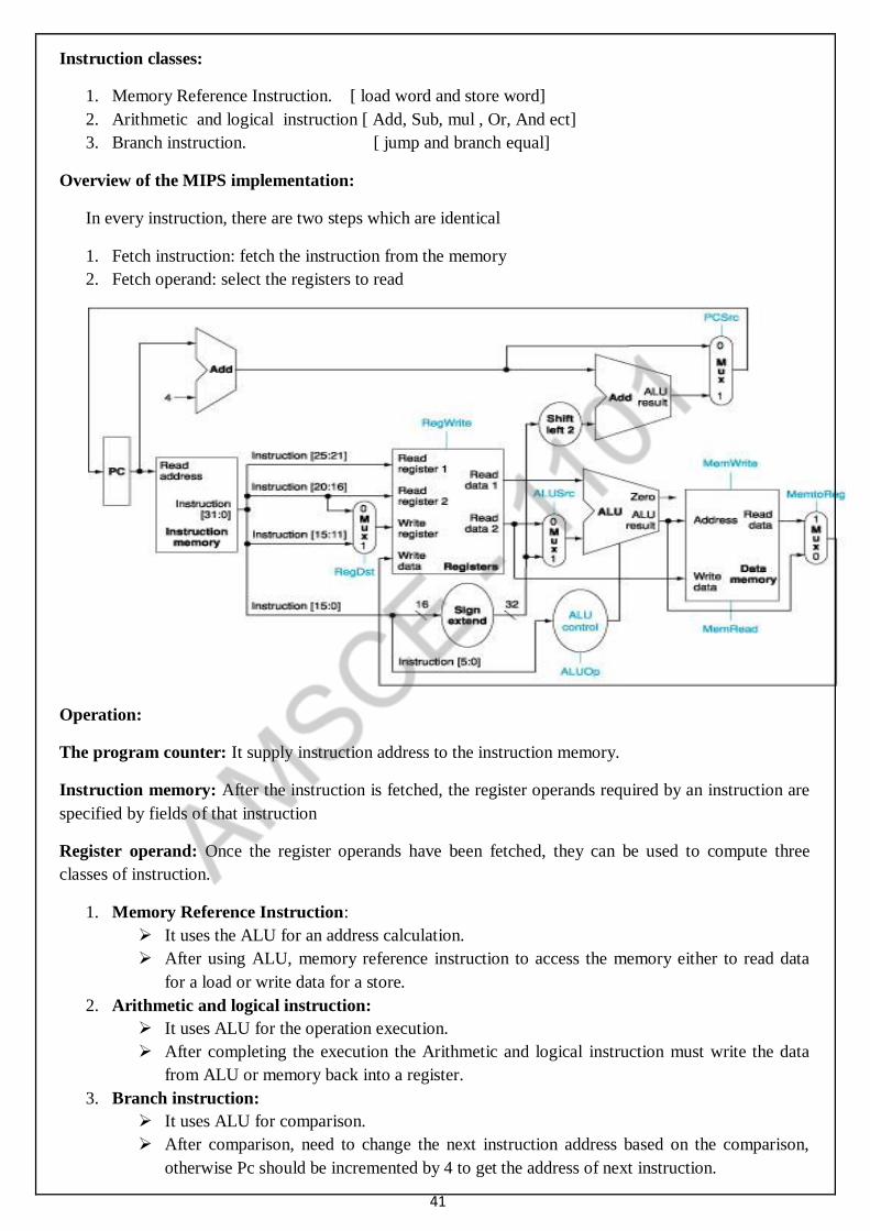
41
Instruction classes:
1. Memory Reference Instruction. [ load word and store word]
2. Arithmetic and logical instruction [ Add, Sub, mul , Or, And ect]
3. Branch instruction. [ jump and branch equal]
Overview of the MIPS implementation:
In every instruction, there are two steps which are identical
1. Fetch instruction: fetch the instruction from the memory
2. Fetch operand: select the registers to read
Operation:
The program counter: It supply instruction address to the instruction memory.
Instruction memory: After the instruction is fetched, the register operands required by an instruction are
specified by fields of that instruction
Register operand: Once the register operands have been fetched, they can be used to compute three
classes of instruction.
1. Memory Reference Instruction:
It uses the ALU for an address calculation.
After using ALU, memory reference instruction to access the memory either to read data
for a load or write data for a store.
2. Arithmetic and logical instruction:
It uses ALU for the operation execution.
After completing the execution the Arithmetic and logical instruction must write the data
from ALU or memory back into a register.
3. Branch instruction:
It uses ALU for comparison.
After comparison, need to change the next instruction address based on the comparison,
otherwise Pc should be incremented by 4 to get the address of next instruction.
42
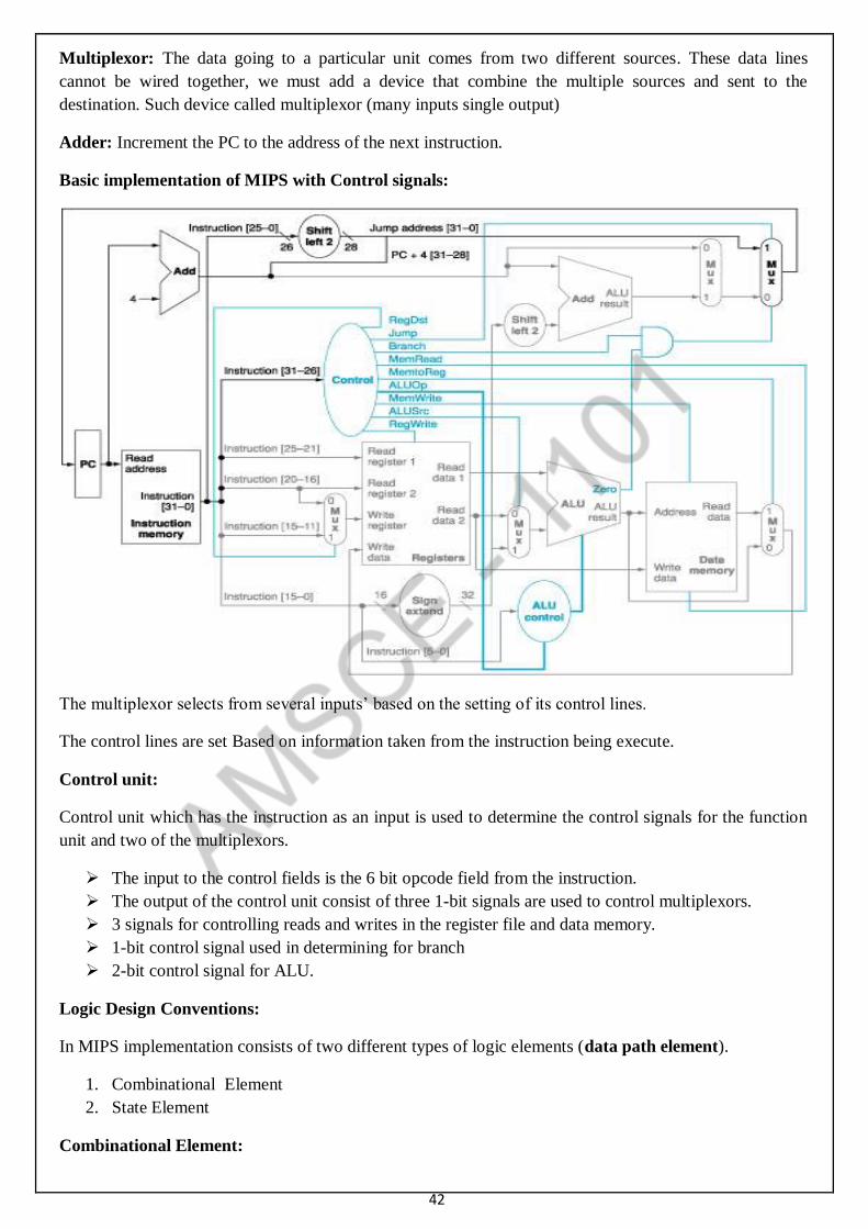
Multiplexor: The data going to a particular unit comes from two different sources. These data lines
cannot be wired together, we must add a device that combine the multiple sources and sent to the
destination. Such device called multiplexor (many inputs single output)
Adder: Increment the PC to the address of the next instruction.
Basic implementation of MIPS with Control signals:
The multiplexor selects from several inputs’ based on the setting of its control lines.
The control lines are set Based on information taken from the instruction being execute.
Control unit:
Control unit which has the instruction as an input is used to determine the control signals for the function
unit and two of the multiplexors.
The input to the control fields is the 6 bit opcode field from the instruction.
The output of the control unit consist of three 1-bit signals are used to control multiplexors.
3 signals for controlling reads and writes in the register file and data memory.
1-bit control signal used in determining for branch
2-bit control signal for ALU.
Logic Design Conventions:
In MIPS implementation consists of two different types of logic elements (data path element).
1. Combinational Element
2. State Element
Combinational Element:
43
The element that operates on data value such as AND gate or an ALU, which means the output
depend only on the current inputs.
State Element:
A memory element such as register or a memory is called as state element.
An element contains state if it has internal storage.
Logical component that contains state are called sequential, because their output depend on both
their inputs and the contents of the internal state.
Clocking Methodology:
It is used to determine when the data is valid and stable relative to the clock.
It specifies the timing of read and writes.
A clocking methodology is designed to ensure predictability.
Edge – triggered clocking Methodology:
Any values stored in a sequential logic element are updated only on a clock edge.
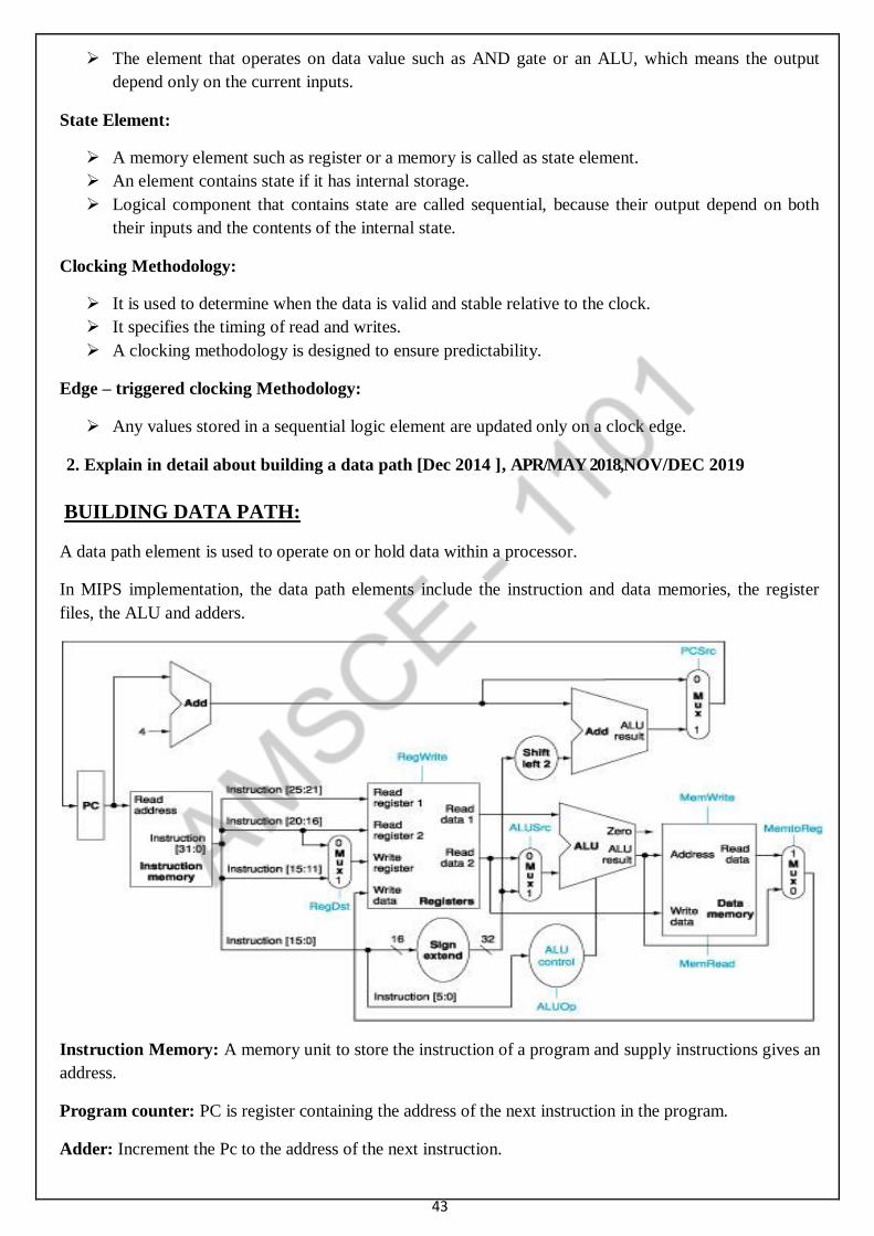
2. Explain in detail about building a data path [Dec 2014 ], APR/MAY 2018,NOV/DEC 2019
BUILDING DATA PATH:
A data path element is used to operate on or hold data within a processor.
In MIPS implementation, the data path elements include the instruction and data memories, the register
files, the ALU and adders.
Instruction Memory: A memory unit to store the instruction of a program and supply instructions gives an
address.
Program counter: PC is register containing the address of the next instruction in the program.
Adder: Increment the Pc to the address of the next instruction.
44
Data segments:
There are three data Segments:
1. Data segment for Arithmetic and logical instruction.
2. Data segment for load word and store word instruction.
3. Data segment for branch instruction.
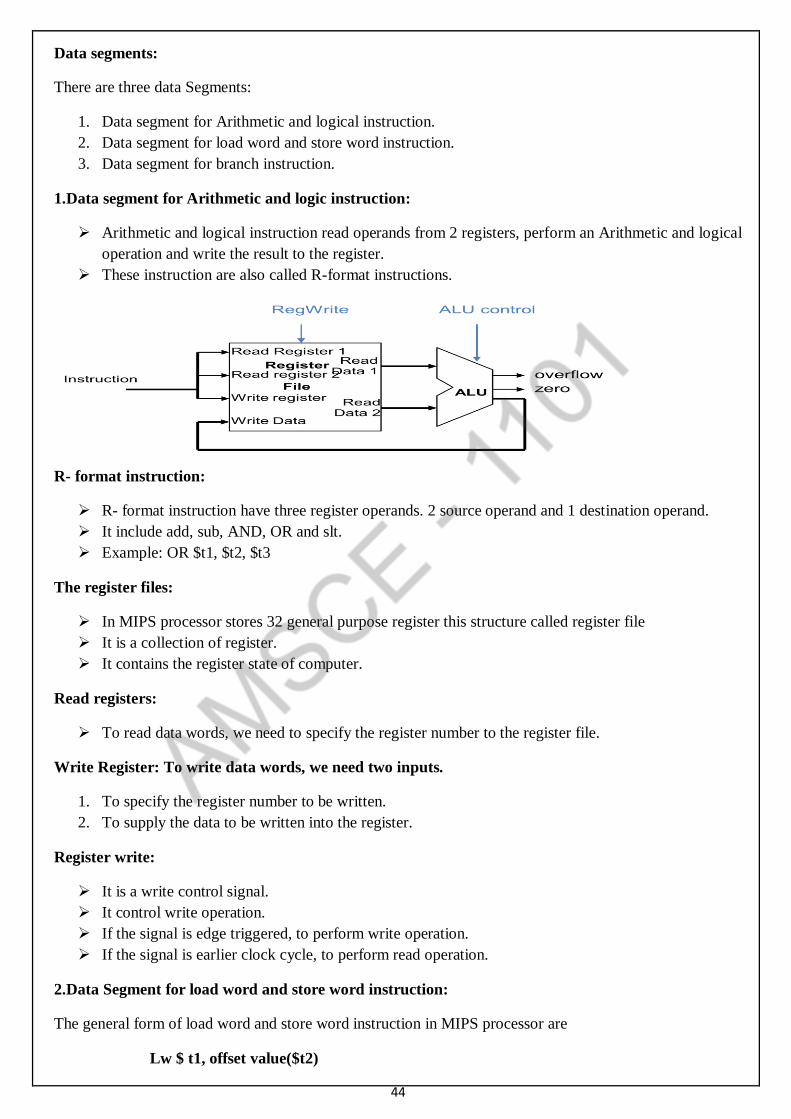
1.Data segment for Arithmetic and logic instruction:
Arithmetic and logical instruction read operands from 2 registers, perform an Arithmetic and logical
operation and write the result to the register.
These instruction are also called R-format instructions.
R- format instruction:
R- format instruction have three register operands. 2 source operand and 1 destination operand.
It include add, sub, AND, OR and slt.
Example: OR $t1, $t2, $t3
The register files:
In MIPS processor stores 32 general purpose register this structure called register file
It is a collection of register.
It contains the register state of computer.
Read registers:
To read data words, we need to specify the register number to the register file.
Write Register: To write data words, we need two inputs.
1. To specify the register number to be written.
2. To supply the data to be written into the register.
Register write:
It is a write control signal.
It control write operation.
If the signal is edge triggered, to perform write operation.
If the signal is earlier clock cycle, to perform read operation.
2.Data Segment for load word and store word instruction:
The general form of load word and store word instruction in MIPS processor are
Lw $ t1, offset value($t2)
45
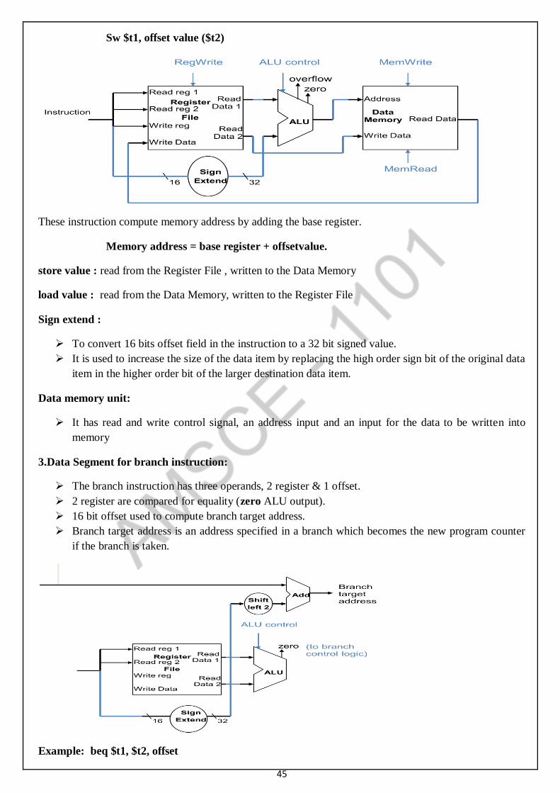
Sw $t1, offset value ($t2)
These instruction compute memory address by adding the base register.
Memory address = base register + offsetvalue.
store value : read from the Register File , written to the Data Memory
load value : read from the Data Memory, written to the Register File
Sign extend :
To convert 16 bits offset field in the instruction to a 32 bit signed value.
It is used to increase the size of the data item by replacing the high order sign bit of the original data
item in the higher order bit of the larger destination data item.
Data memory unit:
It has read and write control signal, an address input and an input for the data to be written into
memory
3.Data Segment for branch instruction:
The branch instruction has three operands, 2 register & 1 offset.
2 register are compared for equality (zero ALU output).
16 bit offset used to compute branch target address.
Branch target address is an address specified in a branch which becomes the new program counter
if the branch is taken.
Example: beq $t1, $t2, offset
46
If the condition is true ,the branch target address becomes new pc and the branch is taken.
If the condition is false, incremented pc should replace the current pc and branch is not taken
The branch data path must perform two operations:
1. Compute the branch target address: the branch data path includes a sign extension unit, shifter and an
adder
2. Compare the register content : used register file and the ALU.
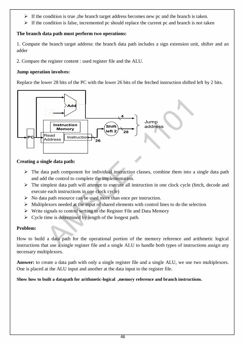
Jump operation involves:
Replace the lower 28 bits of the PC with the lower 26 bits of the fetched instruction shifted left by 2 bits.
Creating a single data path:
The data path component for individual instruction classes, combine them into a single data path
and add the control to complete the implementation.
The simplest data path will attempt to execute all instruction in one clock cycle (fetch, decode and
execute each instructions in one clock cycle)
No data path resource can be used more than once per instruction.
Multiplexors needed at the input of shared elements with control lines to do the selection
Write signals to control writing to the Register File and Data Memory
Cycle time is determined by length of the longest path.
Problem:
How to build a data path for the operational portion of the memory reference and arithmetic logical
instructions that use a single register file and a single ALU to handle both types of instructions assign any
necessary multiplexors.
Answer: to create a data path with only a single register file and a single ALU, we use two multiplexors.
One is placed at the ALU input and another at the data input to the register file.
Show how to built a datapath for arithmetic-logical ,memory reference and branch instructions.
47
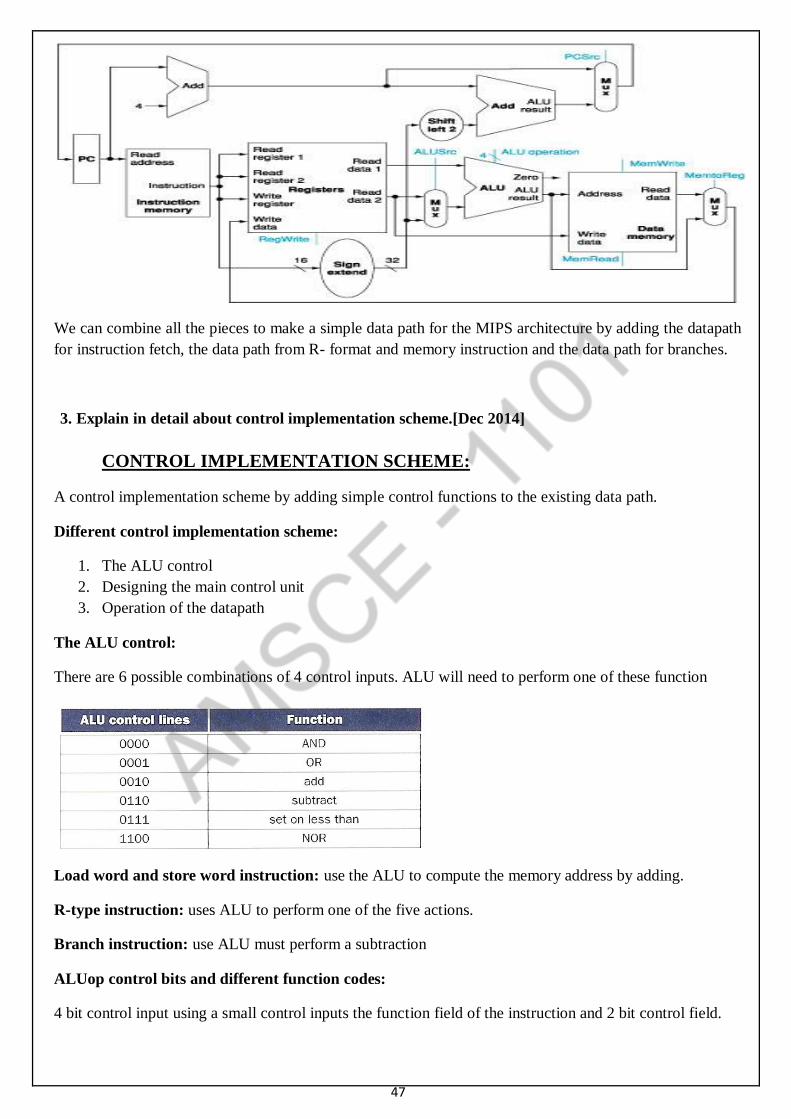
We can combine all the pieces to make a simple data path for the MIPS architecture by adding the datapath
for instruction fetch, the data path from R- format and memory instruction and the data path for branches.
3. Explain in detail about control implementation scheme.[Dec 2014]
CONTROL IMPLEMENTATION SCHEME:
A control implementation scheme by adding simple control functions to the existing data path.
Different control implementation scheme:
1. The ALU control
2. Designing the main control unit
3. Operation of the datapath
The ALU control:
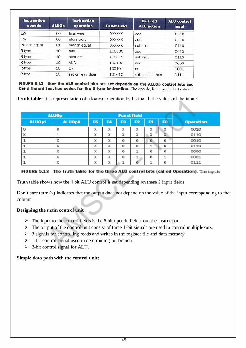
There are 6 possible combinations of 4 control inputs. ALU will need to perform one of these function
Load word and store word instruction: use the ALU to compute the memory address by adding.
R-type instruction: uses ALU to perform one of the five actions.
Branch instruction: use ALU must perform a subtraction
ALUop control bits and different function codes:
4 bit control input using a small control inputs the function field of the instruction and 2 bit control field.
48
Truth table: It is representation of a logical operation by listing all the values of the inputs.
Truth table shows how the 4 bit ALU control is set depending on these 2 input fields.
Don’t care term (x) indicates that the output does not depend on the value of the input corresponding to that
column.
Designing the main control unit :
The input to the control fields is the 6 bit opcode field from the instruction.
The output of the control unit consist of three 1-bit signals are used to control multiplexors.
3 signals for controlling reads and writes in the register file and data memory.
1-bit control signal used in determining for branch
2-bit control signal for ALU.
Simple data path with the control unit:
49
And gate is used to combine the branch control signal and zero output from ALU.
And gate output controls selection of the next PC.
The multiplexor selects the 1 input, the control is asserted.
The multiplexor selects the 0 input, the control is de-asserted.
Seven control signals:
Opcode fields of the instruction:
50
Operation of the datapath:
3 instruction classes which help to understand how to connect the fields of an institution to the data path.
1. Instruction format for R- format instruction, which all have an opcode of 0.
2. Instruction format for load (opcode = 35 ten) and store =43 ten) instruction.
3. Instruction format for branch equal (opcode =4)
Important observation about this instruction format:
Bit 31:26 in the instruction is opcode (op) field
Bit 25:21 and 20:16 in the instruction format alway specify rs and rt .
Bit 25:21 always give the base register (rs) for load and store.
Bit 15:0 give the The 16- bit offset for branch equal,load and store
The destination register is in one or two place.
beq $s1, $s2, L
rs rt4
31:26 25:21 20-16
address
15:0
s1 s2
+subtract
rs rt35 or 43
31:26 25:21 20-16
address
15:0
lw $s1, 100($s2)
sw $s1, 100($s2)
stor
e
baseload
rs rt rd shamt0 funct
31:26 25:21 20-16 15:11 10:6 5:0
s2 s3
++
add $s1, $s2, $s3
s1
51
This figure shows the additions plus the ALU control block, the write signal for state elements, the read
signal for the data memory and the control signals for the multiplexor.
1.Data path for an operation in a R-type instruction:
Data path for an R-type instruction such as
add $t1, $t2,$t3
Four steps needed to execute the instruction:
1. The instruction is fetched and the Pc is incremented.
2. To registers, $t2 and $t3 are read from the register file and main control unit computes the setting of
the control lines during this step.
3. The ALU operates on the data read from the register file, using the function code to generate the
ALU function.
4. The result from the ALU is written into the register file using bits 15:11 of the instruction to select
the destination register ( $ t1)
2.Data path for an operation in a Load instruction:
Data path for an Load word instruction
LW $t2, offsetvalu ($t1)
Five steps needed to execute the instruction:
1. An instruction is fetched from the instruction memory, and the PC is incremented.
2. A register ($t2) value is read form the register file.
3. The ALU computes the sum of the value read from the register file and the sign extended lower 16
bits of the instruction(offset).
4. The sum from the ALU is used as the address for the data memory.
5. The data from the memory units is written into the register files; the Register destination is given by
bits 20:16 of the instruction ($t1).
3.Data path for an operation in a branch –on –equal instruction:
52
Data path for beq instruction
Beq $t1,$t2,offset
Four steps needed to execute the instruction:
1. An instruction is fetched from the instruction memory and the Pc is incremented.
2. Two register $t1,$t2 are read from the register file.
3. The ALU performs a subtract on the data value read from the register file. The value PC+4 is added
to the sign extended , lower 16 bits of the instruction shifted left by two, the result is the branch
target address.
4. The Zero result from the ALU is used to decide which adder result to store into the PC.
Implementing Jumps:
The low-order 2 bits of a jump address are always 00two.
The next lower 26 bits of this 32 bit address come from the 26 bit immediate field in the instruction.
The upper 4 bits of the address replace the Pc come from Pc of the jump plus 4.
Jump by storing into the PC the concatenation of:
1. The upper 4 bit of the current PC+4
2. The 26 bit immediate field of the jump instruction.
3. The bit 00two.
4.WHAT IS PIPELINING AND DISCUSS ABOUT PIPELINED DATA PATH AND CONTROL
MAY/JUNE 2016, NOV/DEC 2014 , APR/MAY 2019,NOV/DEC 2019 ( 16 MARKS )
PIPELINING:
Pipelining is an implementation technique in which multiple instructions are overlapped in execution.
Five steps in a MIPS instruction:
1. IF: Instruction fetch from memory
2. ID: Instruction decode & register read
3. EX: Execute operation or calculate address
4. MEM: Access memory operand
5. WB: Write result back to register
Example:
Assume time for stages is 100ps for register read or write 200ps for other stages. Compare pipelined
datapath with single-cycle datapath
Solution:
000010 address
31:26 25:0
53
Instruction
class
Instruction
fetch
Register read ALU
operation
Data Access Register
write
Total Time
LW 200ps 100ps 200ps 200ps 100ps 800ps
SW 200ps 100ps 200ps 200ps 700ps
R-format 200ps 100ps 200ps 100ps 600ps
Branch 200ps 100ps 200ps 500ps
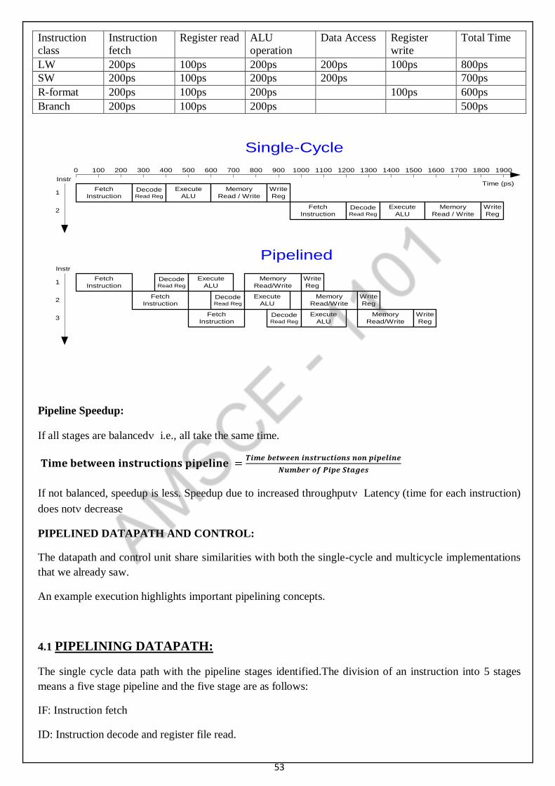
Pipeline Speedup:
If all stages are balanced i.e., all take the same time.
𝐓𝐢𝐦𝐞 𝐛𝐞𝐭𝐰𝐞𝐞𝐧 𝐢𝐧𝐬𝐭𝐫𝐮𝐜𝐭𝐢𝐨𝐧𝐬 𝐩𝐢𝐩𝐞𝐥𝐢𝐧𝐞 =𝑻𝒊𝒎𝒆 𝒃𝒆𝒕𝒘𝒆𝒆𝒏 𝒊𝒏𝒔𝒕𝒓𝒖𝒄𝒕𝒊𝒐𝒏𝒔 𝒏𝒐𝒏 𝒑𝒊𝒑𝒆𝒍𝒊𝒏𝒆
𝑵𝒖𝒎𝒃𝒆𝒓 𝒐𝒇 𝑷𝒊𝒑𝒆 𝑺𝒕𝒂𝒈𝒆𝒔
If not balanced, speedup is less. Speedup due to increased throughput Latency (time for each instruction)
does not decrease
PIPELINED DATAPATH AND CONTROL:
The datapath and control unit share similarities with both the single-cycle and multicycle implementations
that we already saw.
An example execution highlights important pipelining concepts.
4.1 PIPELINING DATAPATH:
The single cycle data path with the pipeline stages identified.The division of an instruction into 5 stages
means a five stage pipeline and the five stage are as follows:
IF: Instruction fetch
ID: Instruction decode and register file read.
Time (ps)Instr
Fetch
InstructionDecodeRead Reg
Execute
ALU
Memory
Read / Write
Write
Reg1
2
0 100 200 300 400 500 600 700 800 900 1100 1200 1300 1400 1500 1600 1700 1800 19001000
Instr
1
2
3
Fetch
InstructionDecodeRead Reg
Execute
ALU
Memory
Read / Write
Write
Reg
Fetch
InstructionDecodeRead Reg
Execute
ALU
Memory
Read/Write
Write
Reg
Fetch
InstructionDecodeRead Reg
Execute
ALU
Memory
Read/Write
Write
Reg
Fetch
InstructionDecodeRead Reg
Execute
ALU
Memory
Read/Write
Write
Reg
Single-Cycle
Pipelined
54
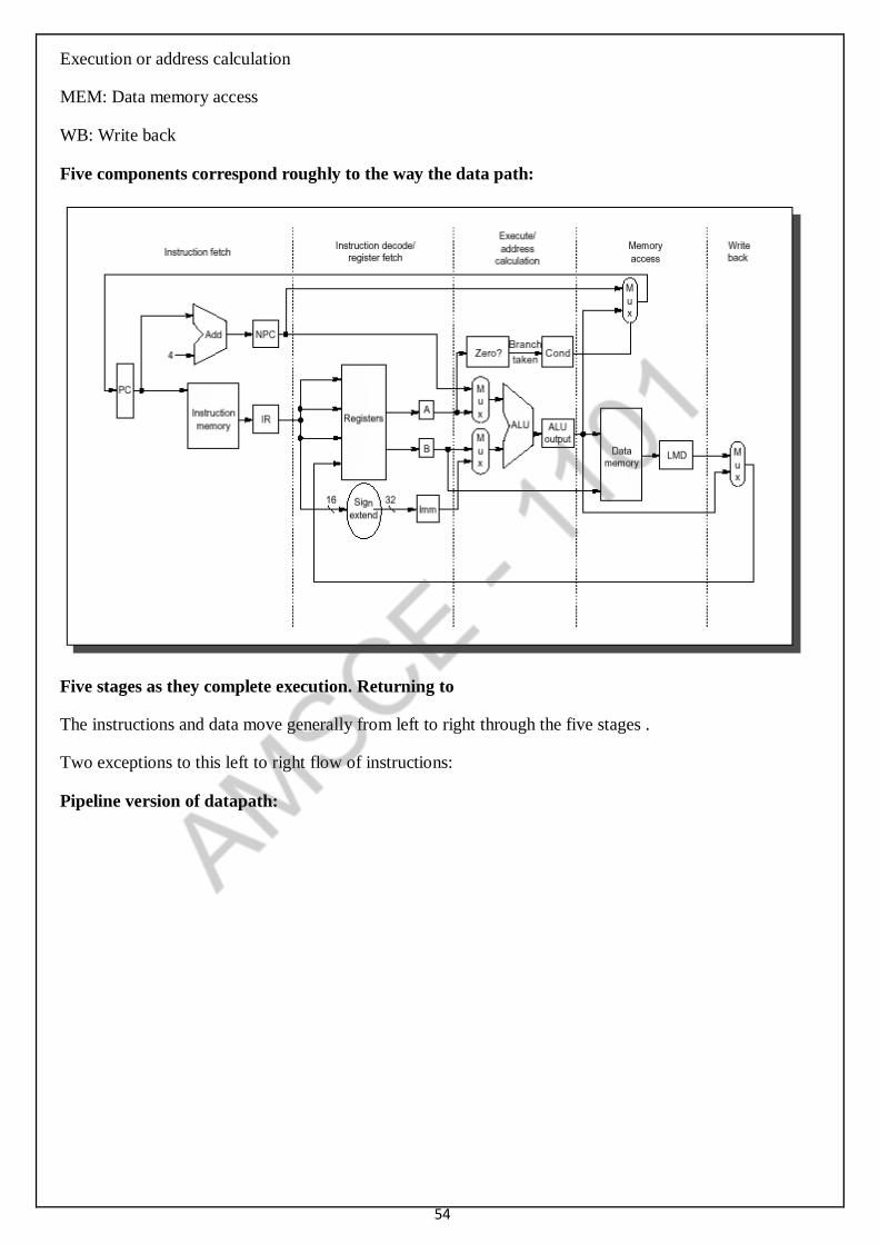
Execution or address calculation
MEM: Data memory access
WB: Write back
Five components correspond roughly to the way the data path:
Five stages as they complete execution. Returning to
The instructions and data move generally from left to right through the five stages .
Two exceptions to this left to right flow of instructions:
Pipeline version of datapath:
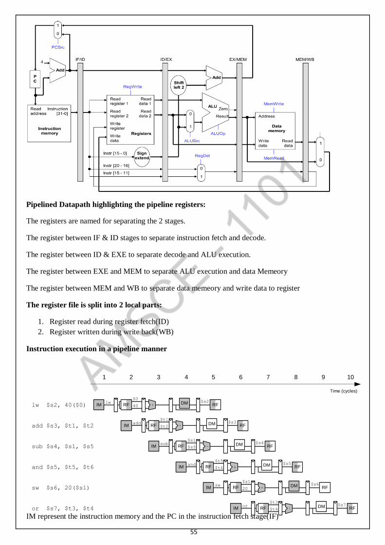
55
Pipelined Datapath highlighting the pipeline registers:
The registers are named for separating the 2 stages.
The register between IF & ID stages to separate instruction fetch and decode.
The register between ID & EXE to separate decode and ALU execution.
The register between EXE and MEM to separate ALU execution and data Memeory
The register between MEM and WB to separate data memeory and write data to register
The register file is split into 2 local parts:
1. Register read during register fetch(ID)
2. Register written during write back(WB)
Instruction execution in a pipeline manner
IM represent the instruction memory and the PC in the instruction fetch stage(IF)
Time (cycles)
lw $s2, 40($0) RF 40
$0
RF$s2
+ DM
RF $t2
$t1
RF$s3
+ DM
RF $s5
$s1
RF$s4
- DM
RF $t6
$t5
RF$s5
& DM
RF 20
$s1
RF$s6
+ DM
RF $t4
$t3
RF$s7
| DM
add $s3, $t1, $t2
sub $s4, $s1, $s5
and $s5, $t5, $t6
sw $s6, 20($s1)
or $s7, $t3, $t4
1 2 3 4 5 6 7 8 9 10
add
IM
IM
IM
IM
IM
IMlw
sub
and
sw
or
56
Reg stand for the register file in the instruction decode/register file read stage
Execution of Load /store instruction in a five stage pipeline:
Stage 1 : Instruction fetch:
The instruction being read from instruction memory using the address in PC and then storing the
instruction in the IF/ID pipeline register.
PC address is incremented by 4 and then write back into PC to read for next clock cycle.
Incremented address is also saved in the IF/ID pipeline register.
Stage 2 :Instruction decode & register file read:
The instruction portion of the IF/ID pipeline register.
It supply the 16 bit immediate field, which is sign extended to 32 bit and the register numbers to
read the 2 registers.
All three values are stored in the ID?EX pipeline register.
Stage 3: Execute and address calculation:
The load instruction reads the contents of register 1 and the sign extended immediate from ID/EX
pipeline register and add them using ALU.
The sum is placed in EX/MEM pipeline register.
Stage 4: Memory access:
The load instruction reading the data memory using the address from the EX/MEM pipeline register
and loading the data into the MEM/WB pipeline registers.
Stage 5: Write Back:
Reading the data from the MEM/WB pipeline register and writing into the register file.
PIPELINED CONTROL:
In pipeline control just add the control to the pipelined data path.
Thus data path borrows the control logic for source, register destination number and ALU control.
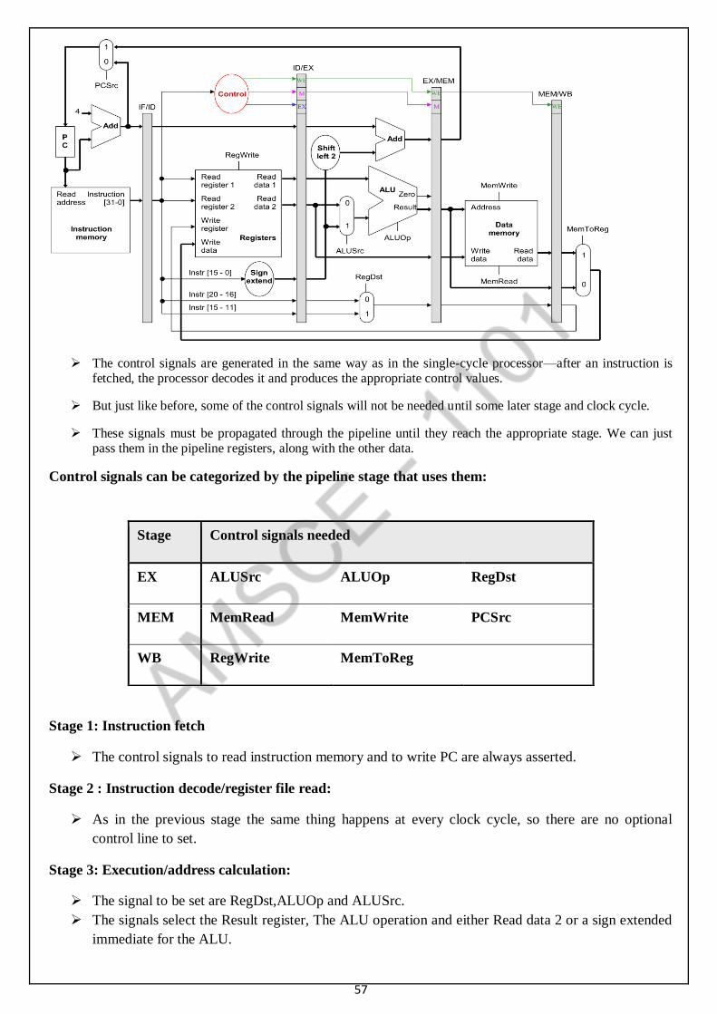
57
The control signals are generated in the same way as in the single-cycle processor—after an instruction is fetched, the processor decodes it and produces the appropriate control values.
But just like before, some of the control signals will not be needed until some later stage and clock cycle.
These signals must be propagated through the pipeline until they reach the appropriate stage. We can just pass them in the pipeline registers, along with the other data.
Control signals can be categorized by the pipeline stage that uses them:
Stage 1: Instruction fetch
The control signals to read instruction memory and to write PC are always asserted.
Stage 2 : Instruction decode/register file read:
As in the previous stage the same thing happens at every clock cycle, so there are no optional
control line to set.
Stage 3: Execution/address calculation:
The signal to be set are RegDst,ALUOp and ALUSrc.
The signals select the Result register, The ALU operation and either Read data 2 or a sign extended
immediate for the ALU.
Stage Control signals needed
EX ALUSrc ALUOp RegDst
MEM MemRead MemWrite PCSrc
WB RegWrite MemToReg
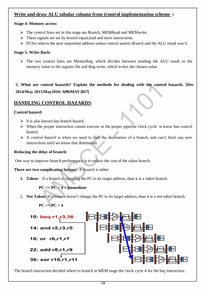
58
Write and draw ALU tabular column from (control implementation scheme_)
Stage 4: Memory access:
The control lines set in this stage are Branch, MEMRead and MEMwrite.
These signals are set by branch equal,load and store instructions.
PCSrc selects the next sequential address unless control asserts Branch and the ALU result was 0.
Stage 5: Write Back:
The two control lines are MemtoReg, which decides between sending the ALU result or the
memory value to the register file and Reg-write, which writes the chosen value.
5. What are control hazards? Explain the methods for dealing with the control hazards. [Dec
2014/May 2015/May2016/ APR/MAY 2017]
HANDLING CONTROL HAZARDS:
Control hazard:
It is also known has branch hazard.
When the proper instruction cannot execute in the proper pipeline clock cycle is know has control
branch.
A control hazard is when we need to find the destination of a branch, and can’t fetch any new
instructions until we know that destination.
Reducing the delay of branch:
One way to improve branch performance is to reduce the cost of the taken branch.
There are two complicating factors: A branch is either
1. Taken: If a branch is changing the PC to its target address, than it is a taken branch.
PC <= PC + 4 + Immediate
2. Not Taken: If a branch doesn’t change the PC to its target address, than it is a not taken branch.
PC <= PC + 4
The branch instruction decided where to branch in MEM stage the clock cycle 4 for the beq instruction.
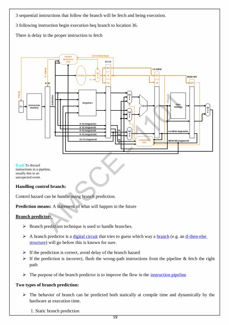
59
3 sequential instructions that follow the branch will be fetch and being execution.
3 following instruction begin execution beq branch to location 36.
There is delay in the proper instruction to fetch
fl ush To discard instructions in a pipeline, usually due to an unexpected event.
Handling control branch:
Control hazard can be handle using branch prediction.
Prediction means: A statement of what will happen in the future
Branch predictor:
Branch prediction technique is used to handle branches.
A branch predictor is a digital circuit that tries to guess which way a branch (e.g. an if-then-else
structure) will go before this is known for sure.
If the prediction is correct, avoid delay of the branch hazard
If the prediction is incorrect, flush the wrong-path instructions from the pipeline & fetch the right
path
The purpose of the branch predictor is to improve the flow in the instruction pipeline
Two types of branch prediction:
The behavior of branch can be predicted both statically at compile time and dynamically by the
hardware at execution time.
1. Static branch prediction
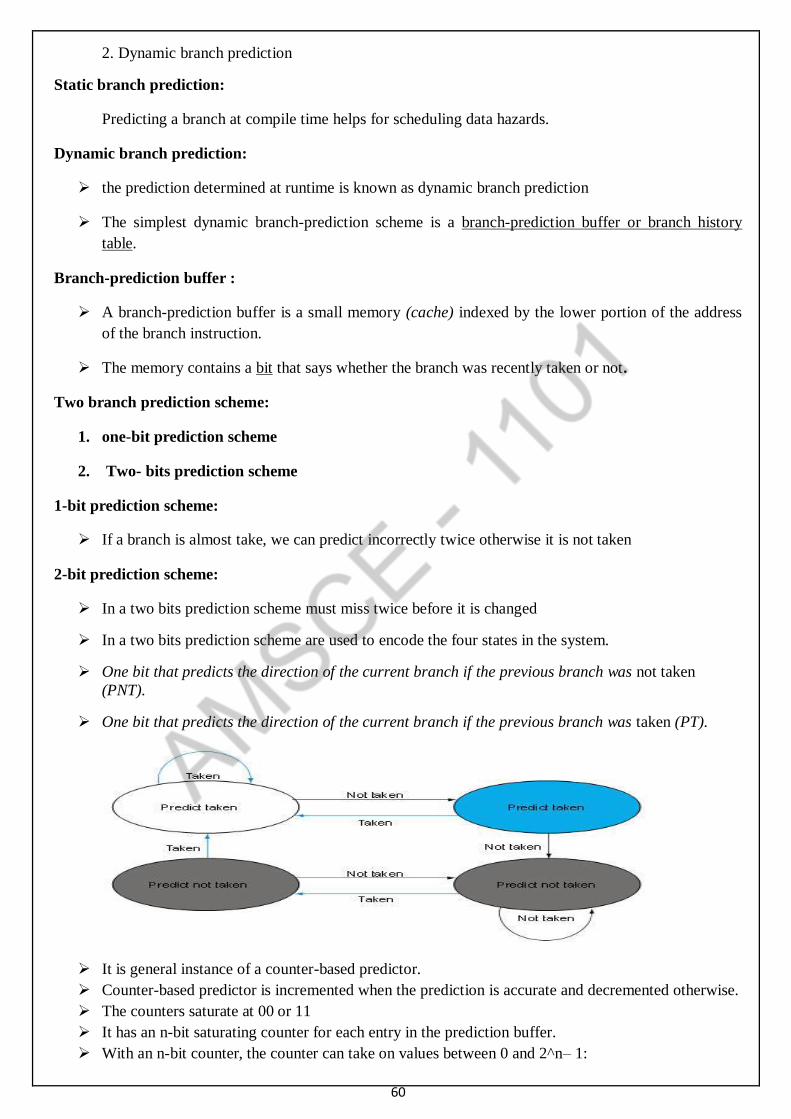
60
2. Dynamic branch prediction
Static branch prediction:
Predicting a branch at compile time helps for scheduling data hazards.
Dynamic branch prediction:
the prediction determined at runtime is known as dynamic branch prediction
The simplest dynamic branch-prediction scheme is a branch-prediction buffer or branch history
table.
Branch-prediction buffer :
A branch-prediction buffer is a small memory (cache) indexed by the lower portion of the address
of the branch instruction.
The memory contains a bit that says whether the branch was recently taken or not.
Two branch prediction scheme:
1. one-bit prediction scheme
2. Two- bits prediction scheme
1-bit prediction scheme:
If a branch is almost take, we can predict incorrectly twice otherwise it is not taken
2-bit prediction scheme:
In a two bits prediction scheme must miss twice before it is changed
In a two bits prediction scheme are used to encode the four states in the system.
One bit that predicts the direction of the current branch if the previous branch was not taken
(PNT).
One bit that predicts the direction of the current branch if the previous branch was taken (PT).
It is general instance of a counter-based predictor.
Counter-based predictor is incremented when the prediction is accurate and decremented otherwise.
The counters saturate at 00 or 11
It has an n-bit saturating counter for each entry in the prediction buffer.
With an n-bit counter, the counter can take on values between 0 and 2^n– 1:
61
When the counter is greater than or equal to one half of its maximum value (2^n–1), the branch is
predicted as taken; otherwise, it is predicted untaken.
branch delay slot:
The slot directly aft era delayed branch instruction, which in the MIPS architecture is filled by an
instruction that does not affect the branch.
Compilers and assemblers try to place an instruction that always executes after the branch in the
branch delay slot.
The job of the software is to make the successor instructions valid and useful.
Three ways in which the branch delay slot can be scheduled:
The top box in each pair shows the code before scheduling; the bottom box shows the scheduled code.
In (a), the delay slot is scheduled with an independent instruction from before the branch. This is the best
choice. Strategies (b) and (c) are used when (a) is not possible.
In the code sequences for (b) and (c), the use of $s1 in the branch condition prevents the add instruction
(whose destination is $s1) from being moved into the branch delay slot.
In (b) the branch delay slot is scheduled from the target of the branch; usually the target instruction will
need to be copied because it can be reached by another path.
Strategy (b) is preferred when the branch is taken with high probability, such as a loop branch.
Finally, the branch may be scheduled from the not-taken fall-through as in (c).
To make this optimization legal for (b) or (c), it must be OK to execute the sub instruction when the branch
goes in the unexpected direction.
By “OK” we mean that the work is wasted, but the program will still execute correctly.
6. Discuss the data hazards and forwarding in pipelining [Dec 2014/May2015/May2016]
62
PIPELINE HAZARDS:A pipeline hazard refers to situations that prevent an instruction from
entering the next stage is called hazard.
3 different types of hazard: 1. Structural hazards
2. Data hazards
3. Control hazards
Structural hazards - Attempt to use the same resource by two or more instructions at the same time
Control hazards - attempt to make branching decisions before branch condition is evaluated
Data hazards – When wither the source or destination operands of an instruction are not available at time
expected in the pipeline and as a result pipeline is stalled. This situation is a data hazard.
Let’s look at a sequence with many dependences,:
sub $2, $1,$3 # Register $2 written by sub
and $12,$2,$5 # 1st operand($2) depends on sub
or $13,$6,$2 # 2nd operand($2) depends on sub
add $14,$2,$2 # 1st($2) & 2nd($2) depend on sub
sw $15,100($2) # Base ($2) depends on sub
The last four instructions are all dependent on the result in register $2 of the first instruction. If register $2
had the value 10 before the subtract instruction and −20 afterwards, the programmer intends that −20 will
be used in the following instructions that refer to register $2.
HANDLING DATA HAZARD: Forwarding versus Stalling
Data hazards occur when the pipeline changes the order of read/write accesses to operands that differs from
the normal sequential order
Forwarding (bypassing) with two instructions:
It is also known as bypassing.
This is a method resolving a data hazard by retrieving the missing data element from the internal
buffer rather than waiting for it to arrive from the memory.
Graphical Representation of Forwarding:
It show the connection to forward the value in $s0 after the execution stage of the add instruction.
63
Forwarding paths are valid only if the destination stage is later in time than source stage.
Forwarding cannot prevent all pipeline stalls. They are also often referred to as bubbles in the pipeline.
Forwarding versus stalling:
Data hazard with a sequence of many dependencies
Sub $2, $1, $3 # register $2 written by sub
and $12, $2, $5 # 1st operand ($2) depends on sub
or $13, $6, $2 # 2nd operand ($2) depends on sub
add $14, $2, $2 # 1st ($2) & 2nd ($2) depend on sub
sw $15, 100($2) # base ($2) depends on sub
The last four instructions are all dependent on the result in register $2 of the first instruction.
If the register $2 had the value 10 before the subtraction instruction and -20 afterwards, the programmer
intends -20 will be used in the following instruction that refer to register $2.
Pipelined Dependences in a five instruction sequence:
This diagram illustrates the execution of these instructions using a multiple clock cycle pipeline
representation.
Hazard condition: HAZARD DETECTION UNIT
The two pairs of hazard conditions are
1a: EX/MEM.RegisterRd = ID/EX.RegisterRs
1b: EX/MEM.RegisterRd = ID/EX.RegisterRt
2a: MEM/WB.RegisterRd = ID/EX.RegisterRs
2b: MEM/WB.RegisterRd = ID/EX.RegisterRt
The first hazard in the sequence is one register $2, between the result of sub $2 $1 $3 and the first read
operand of and $12,$2,$5.This hazard can be detected when and instruction is the EX stage and the prior
instruction is in the MEM stage
IM Reg
IM Reg
CC 1 CC 2 CC 3 CC 4 CC 5 CC 6
Time (in clock cycles)
sub $2, $1, $3
Program
execution
order
(in instructions)
and $12, $2, $5
IM Reg DM Reg
IM DM Reg
IM DM Reg
CC 7 CC 8 CC 9
10 10 10 10 10/– 20 – 20 – 20 – 20 – 20
or $13, $6, $2
add $14, $2, $2
sw $15, 100($2)
Value of
register $2:
DM Reg
Reg
Reg
Reg
DM
64
EX/MEM.Register RD= ID?EX.RegisreRs=$2.
The sub-or is a type 2b hazard:
MEM/WB.RegisterRd = ID/EX.RegisterRt = $2
■ The two dependences on sub-add are not hazards because the register file supplies the proper data during
the ID stage of add.
■ There is no data hazard between sub and sw because sw reads $2 the clock cycle after sub writes $2.
Can forward only to the “or” and “add” instructions without stalling $2 still unavailable in EX/MEM for
“and”. When sub was the “writing” instruction, we forwarded from EX/MEM to the ALU for “and”
The multiplexors have been expanded to add the forwarding paths, and we show the forwarding
unit.
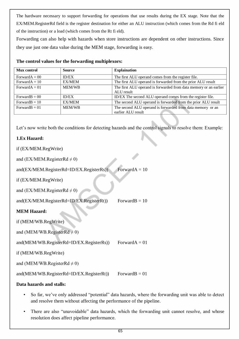
65
The hardware necessary to support forwarding for operations that use results during the EX stage. Note that the
EX/MEM.RegisterRd field is the register destination for either an ALU instruction (which comes from the Rd fi eld
of the instruction) or a load (which comes from the Rt fi eld).
Forwarding can also help with hazards when store instructions are dependent on other instructions. Since
they use just one data value during the MEM stage, forwarding is easy.
The control values for the forwarding multiplexors:
Let’s now write both the conditions for detecting hazards and the control signals to resolve them: Example:
1.Ex Hazard:
if (EX/MEM.RegWrite)
and (EX/MEM.RegisterRd ≠ 0)
and(EX/MEM.RegisterRd=ID/EX.RegisterRs)) ForwardA = 10
if (EX/MEM.RegWrite)
and (EX/MEM.RegisterRd ≠ 0)
and(EX/MEM.RegisterRd=ID/EX.RegisterRt)) ForwardB = 10
MEM Hazard:
if (MEM/WB.RegWrite)
and (MEM/WB.RegisterRd ≠ 0)
and(MEM/WB.RegisterRd=ID/EX.RegisterRs)) ForwardA = 01
if (MEM/WB.RegWrite)
and (MEM/WB.RegisterRd ≠ 0)
and(MEM/WB.RegisterRd=ID/EX.RegisterRt)) ForwardB = 01
Data hazards and stalls:
• So far, we’ve only addressed “potential” data hazards, where the forwarding unit was able to detect
and resolve them without affecting the performance of the pipeline.
• There are also “unavoidable” data hazards, which the forwarding unit cannot resolve, and whose
resolution does affect pipeline performance.
Mux control Source Explaination
ForwardA = 00 ID/EX The first ALU operand comes from the register file.
ForwardA = 10 EX/MEM The first ALU operand is forwarded from the prior ALU result
ForwardA = 01 MEM/WB The first ALU operand is forwarded from data memory or an earlier
ALU result
ForwardB = 00 ID/EX ID/EX The second ALU operand comes from the register file.
ForwardB = 10 EX/MEM The second ALU operand is forwarded from the prior ALU result
ForwardB = 01 MEM/WB The second ALU operand is forwarded from data memory or an
earlier ALU result
66
• We thus add a (unavoidable) hazard detection unit, which detects them and introduces stalls to
resolve them.
Forwarding technique is used to minimize data hazard:
In the load instruction the data is read from memory in clock cycle 4. While the Alu perform the operation
for the following instruction. sometimes the stall the pipeline for the combination of load.
7.How exceptions are handled in MIPS?
EXCEPTIONS:
One of the difficult parts of control is to implement exceptions and interrupts.
Exceptions are generally generated unscheduled events that disrupt program execution and they
have used to detect overflow.
exception Also called interrupt.
Interrupt comes from outside of the processor.
An interrupts is an exception that comes from outside of the processor:
Type of event From where MIPS terminology
I/O device request External Interrupt
Invoke the operating
syster from user
Internal Exception
Arithmetic overflow Internal Exception
Hardware malfunction Either Exception or interrups
Handling Exception in the MIPS architecture:
Types of exception:
1. Execution of an undefined instruction.
2. Arithmetic overflow in the instruction add $1, $2, $1.
lw $2, 20($1)
Program
execution
order
(in instructions)
and $4, $2, $5
or $8, $2, $6
add $9, $4, $2
slt $1, $6, $7
Reg
IM
Reg
Reg
IM DM
CC 1 CC 2 CC 3 CC 4 CC 5 CC 6
Time (in clock cycles)
IM Reg DM RegIM
IM DM Reg
IM DM Reg
CC 7 CC 8 CC 9 CC 10
DM Reg
RegReg
Reg
bubble
67
Reponses to an exception:
When an exception occurs the processor save the address of the offending instruction in the Exception
Program Counter ( EPC) and transfer control to the OS at some specified address.
The OS take the appropriate action, which involve providing some service to the user program, taking
some predefined action in response to an exception or stopping the execution of the program and reporting
an error.
Methods used to communicate the reason for an exception:
To handling the exception it is must for the OS to know the reason for the exception.
Two main methods used to communicate the reason for an exception:
1. Status register method
2. Vectored interrupts method
Status register method: the MIPS architecture uses a status register which holds a field that indicates the
reason for the exception.
Vectored interrupts method: In a vectored interrupt the address to which control is transferred is
determined by the cause of the exception.
Exception in a pipelined implementation:
A pipelined implementation treats exceptions as another form of control hazard.
In pipeline computers interrupt and exceptions are further classified as:
1. Imprecise interrupts or imprecise exceptions
2. Precise interrupts or precise exceptions
Imprecise interrupts or imprecise exceptions:
In pipelined computers that are not associated with the exact instruction that war the cause of the interrupt
or exception is called imprecise interrupts or imprecise exceptions
Precise interrupts or precise exceptions:
An interrupt or exception that is always associated with the correct instruction in pipeline computer called
precise interrupts or precise exceptions.
UNIT-IV PARALLELISM
1. What is meant by ILP?[Dec 2015/May 2016]
Pipelining exploits the potential parallelism among instructions. This parallelism is called
instruction-level parallelism (ILP). There are two primary methods for increasing the potential amount of
instruction-level parallelism.
1. Increasing the depth of the pipeline to overlap more instructions.
2. Multiple issue.
68
2. What is multiple issue? Write any two approaches.
Multiple issue is a scheme whereby multiple instructions are launched in one clock cycle. It is a
method for increasing the potential amount of instruction-level parallelism. It is done by replicating the
internal components of the computer so that it can launch multiple instructions in every pipeline stage.
The two approaches are:
1. Static multiple issue (at compile time)
2. Dynamic multiple issue (at run time)
3. What is meant by speculation?[Dec 2014]
One of the most important methods for finding and exploiting more ILP is speculation. It is an
approach whereby the compiler or processor guesses the outcome of an instruction to remove it as
dependence in executing other instructions. For example, we might speculate on the outcome of a branch,
so that instructions after the branch could be executed earlier.
4. Define Static Multiple Issue?
Static multiple issue is an approach to implement a multiple-issue processor where many decisions
are made by the compiler before execution.
5. Define Issue Slots and Issue Packet?
Issue slots are the positions from which instructions could be issued in a given clock cycle. By
analogy, these correspond to positions at the starting blocks for a sprint. Issue packet is the set of
instructions that issues together in one clock cycle; the packet may be determined statically by the compiler
or dynamically by the processor.
6. Define VLIW?
Very Long Instruction Word (VLIW) is a style of instruction set architecture that launches many
operations that are defined to be independent in a single wide instruction, typically with many separate
opcode fields.
7. Define Superscalar Processor?[Dec 2015]
Superscalar is an advanced pipelining technique that enables the processor to execute more than
one instruction per clock cycle by selecting them during execution. Dynamic multiple-issue processors are
also known as superscalar processors, or simply superscalars.
8. What is meant by loop unrolling?
An important compiler technique to get more performance from loops is loop unrolling, where multiple
copies of the loop body are made. After unrolling, there is more ILP available by overlapping instructions
from different iterations.
9. What is meant by anti-dependence? How is it removed?
Anti-dependence is an ordering forced by the reuse of a name, typically a register, rather than by a true
dependence that carries a value between two instructions. It is also called as name dependence. Register
renaming is the technique used to remove anti-dependence in which the registers are renamed by the
compiler or hardware.
10. What is the use of reservation station and reorder buffer?
69
Reservation station is a buffer within a functional unit that holds the operands and the operation. Reorder
buffer is the buffer that holds results in a dynamically scheduled processor until it is safe to store the results
to memory or a register
11. Differentiate in-order execution from out-of-order execution.
Out-of-order execution is a situation in pipelined execution when an instruction is blocked from executing
does not cause the following instructions to wait. It preserves the data flow order of the program. In-order
execution requires the instruction fetch and decode unit to issue instructions in order, which allows
dependences to be tracked, and requires the commit unit to write results to registers and memory in
program fetch order. This conservative mode is called in-order commit.
12. What is meant by hardware multithreading?[Dec 2014]
Hardware multithreading allows multiple threads to share the functional units of a single processor in
an overlapping fashion to try to utilize the hardware resources efficiently. To permit this sharing, the
processor must duplicate the independent state of each thread. It Increases the utilization of a processor
13. What are the two main approaches to hardware multithreading?
There are two main approaches to hardware multithreading. Fine-grained multithreading switches
between threads on each instruction, resulting in interleaved execution of multiple threads. This
interleaving is often done in a round-robin fashion, skipping any threads that are stalled at that clock cycle.
Coarse-grained multithreading is an alternative to fine-grained multithreading. It switches threads only on
costly stalls, such as last-level cache misses.
14. What is SMT?
Simultaneous Multithreading (SMT) is a variation on hardware multithreading that uses the resources of a
multiple-issue, dynamically scheduled pipelined processor to exploit thread-level parallelism. It also
exploits instruction level parallelism.
15. Differentiate SMT from hardware multithreading.
Since SMT relies on the existing dynamic mechanisms, it does not switch resources every cycle. Instead,
SMT is always executing instructions from multiple threads, leaving it up to the hardware to associate
instruction slots and renamed registers with their proper threads.
16. What are the three multithreading options?
The three multithreading options are:
1. A superscalar with coarse-grained multithreading
2. A superscalar with fine-grained multithreading
3. A superscalar with simultaneous multithreading
17. Define – SMP APR/MAY 2019
Shared memory multiprocessor (SMP) is one that offers the programmer a
single physical address space across all processors – which is nearly always the case for multicore
chips. Processors communicate through shared variables in memory, with all processors capable of
accessing any memory location via loads and stores.
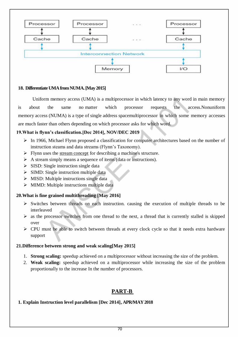
70
18. Differentiate UMA from NUMA. [May 2015]
Uniform memory access (UMA) is a multiprocessor in which latency to any word in main memory
is about the same no matter which processor requests the access.Nonuniform
memory access (NUMA) is a type of single address spacemultiprocessor in which some memory accesses
are much faster than others depending on which processor asks for which word.
19.What is flynn’s classification.[Dec 2014], NOV/DEC 2019
In 1966, Michael Flynn proposed a classification for computer architectures based on the number of
instruction steams and data streams (Flynn’s Taxonomy).
Flynn uses the stream concept for describing a machine's structure.
A stream simply means a sequence of items (data or instructions).
SISD: Single instruction single data
SIMD: Single instruction multiple data
MISD: Multiple instructions single data
MIMD: Multiple instructions multiple data
20.What is fine grained multithreading [May 2016]
Switches between threads on each instruction. causing the execution of multiple threads to be
interleaved
as the processor switches from one thread to the next, a thread that is currently stalled is skipped
over
CPU must be able to switch between threads at every clock cycle so that it needs extra hardware
support
21.Difference between strong and weak scaling[May 2015]
1. Strong scaling: speedup achieved on a multiprocessor without increasing the size of the problem.
2. Weak scaling: speedup achieved on a multiprocessor while increasing the size of the problem
proportionally to the increase In the number of processors.
PART-B
1. Explain Instruction level parallelism [Dec 2014], APR/MAY 2018
71
Parallel computing is a form of computation in which many calculations are carried out simultaneously.
Operation on the principle that are large problems can often be divided into smaller ones which are then
solved concurrently.
Different forms of parallel computing:
Bit level parallelism
Data parallelism
Instruction level parallelism
Task parallelism
1. INSTRUCTION LEVEL PARALLELISM:
The potential overlap among instruction is called Instruction level parallelism(ILP).
This technique which is used to overlap the execution of instructions to improve performance.
Pipeline exploits the instruction level parallelism.
Two primary method for increasing the potential amount of ILP:
1. By increasing the depth of the pipeline to overlap more instructions.
2. By replicating the internal components of the computer so that it can launch
multiple instructions in every pipeline stage.
Such multiple instructions are launched in one clock cycle is known as multiple issue.
Implementation a multiple-issue processor:
Two ways to implementation a multiple issue processor:
1. Static multiple issue: here the decisions of division of work are being made statically (at compile
time)
2. Dynamic multiple issue: here the decisions of division of work are being made dynamically (at run
time)
There are two primary and distinct responsibilities that must be dealt with in a multiple-issue
pipeline:
1. Packaging instructions into issue slots the positions from which instructions could issue in a
given clock cycle.
2. Dealing with data and control hazard.
SPECULATION:
is an approach that allows the compiler or processor to guess the properties of an instruction. So as to
enable execution of other instructions that may depend on the speculation instruction.
72
Example: we might speculate the result of branch, so that the instruction after the branch could be
executed earlier.
Need for speculation:
1. It is most important method for finding and exploiting more ILP.
2. Speculation may be wrong , It is necessary include a method to check if the guess was right or
wrong and a method to undo the effects of the instruction that were executed speculatively this
implementation of this undo capability add complexity.
Speculation may be done in the compiler or by the hardware.
1. Compiler can use speculation to reorder instruction.
2. The processor hardware can reorder instructions at runtime.
Recovery mechanism:
In case of compiler speculation: additional instructions are inserted to check the accuracy of the
speculation and provide a recovery routine to use when the speculation is incorrect.
In case of hardware speculation: the processor usually use buffers to temporary store the speculative
results.
(i) If speculation is correct, the instructions as executed by allowing the contents of the
buffers to be written to the registers or memory.
(ii) If speculation is incorrect the special hardware is used to flush the buffers and execute the
correct instruction sequence.
Static multiple issue:
Static multiple issue processors all use the compiler to assist with packaging instruction and handling
hazards.
A static multiple issue processor usually launches many operations that are defined to be independent in
a signal wide instruction, typically with many separate opcode fields. Such a style of instruction set
architecture is known as very long instruction word(VLIW).
Loop Level Parallelism:
The simplest and most common way to increase the amount of parallelism available among instructions is
to exploit parallelism among iterations in a loop called LLP
Example:
Addition of two 1000-elements arrays that is completely parallel
For(i=0;i<=1000;i=i+1)
x[i]=x[i]+y[i];
Every iteration of loop can overlap with any other iteration.
Example 2:
for (i=1; i<=100; i= i+1)
73
{
a[i] = a[i] + b[i]; //s1
b[i+1] = c[i] + d[i]; //s2
}
Statement s1 uses the value assigned in the previous iteration by statement s2, so there is a loop-carried
dependency between s1 and s2.
Despite this dependency, this loop can be made parallel because the dependency is not circular:
- neither statement depends on itself;
- while s1 depends on s2, s2 does not depend on s1.
Dynamic multiple issue:
Dynamic multiple-issue processors are also known as superscalar processors, or simply superscalar’s.
Superscalar processor:
An advanced pipelining technique that enables the processor to execute more than one instruction per
clock cycle by selecting them during execution.
A simplest superscalar processor:
Instructions issue in order, and the processor decides whether zero, one, or more instructions can issue in
a given clock cycle.
Dynamic pipeline scheduling:
Many superscalar’s extend the basic framework of dynamic issue decisions to include dynamic
pipeline scheduling.
Dynamic pipeline scheduling chooses which instructions to execute in a given clock cycle
while trying to avoid hazards and stalls.
Let’s start with a simple example of avoiding a data hazard.
lw $t0, 20($s2)
addu $t1, $t0, $t2
sub $s4, $s4, $t3
slti $t5, $s4, 20
Even though the sub instruction is ready to execute, it must wait for the lw and addu to complete first,
which might take many clock cycles if memory is slow.
Dynamic pipeline scheduling allows such hazards to be avoided either fully or partially.
The three primary units of a dynamically scheduled pipeline.
1. Instruction fetch and decode unit
2. Functional units
3. Commit unit
Instruction fetches and decode unit
The first unit fetches instructions, decodes them, and sends each instruction to a corresponding
functional unit for execution.
74
Functional units
Each functional unit has buffers, called reservation stations.
Reservation stations: which hold the operands and the operation.
As soon as the buffer contains all its operands and the functional unit is ready to execute, the result is
calculated.
When the result is completed, it is sent to any reservation stations waiting for this particular result as well
as to the commit unit, which buffers the result until it is safe to put the result into the register file or, for a
store, into memory.
Commit unit:
The unit in a dynamic or out-of-order execution pipeline that decides when it is safe to release the result of
an operation to programmer visible registers and memory.
The buffer in the commit unit, oft en called the reorder buffer.
Reorder buffer: is also used to supply operands, in much the same way as forwarding logic does in a
statically scheduled pipeline
out-of-order execution: The processor then executes the instructions in some order that preserves the data flow order of the
program. This style of execution is called an out-of-order execution, since the instructions can be
executed in a different order than they were fetched.
In-order commit:
A commit in which the results of pipelined execution are written to the programmer visible
state in the same order that instructions are fetched.
To make programs behave as if they were running on a simple in-order pipeline, the instruction fetch and
decode unit is required to issue instructions in order, which allows dependences to be tracked, and the
commit unit is required to write results to registers and memory in program fetch order.
Various types of Dependences in ILP:
1.Data dependences (also called true data dependences)
2.Name dependences
3.Control dependences
1.Data dependences
InstrJ is data dependent on InstrI
InstrJ tries to read operand before InstrI writes it
• or InstrJ is data dependent on InstrK which is dependent on InstrI
• Caused by a “True Dependence” (compiler term)
• If true dependence caused a hazard in the pipeline, called a Read After Write (RAW)
Name Dependency:
The name dependence occurs when two instructions use the same register or memory location, called a
name, but there is no flow of data between the instructions associated with that name.
There are two types of name dependences:
1. An anti dependence between instruction i and instruction j occurs when instruction j writes a
75
register or memory location that instruction i reads. The original ordering must be
preserved to ensure that i reads the correct value.
2. An output dependence occurs when instruction i and instruction j write the same register or
memory location. The ordering between the instructions must be preserved to ensure that the
value finally written corresponds to instruction j.
Register Renaming:
Renaming can be more easily done for register operands, where it is called register renaming.
Register renaming can be done either statically by a compiler or dynamically by the hardware.
Before describing dependences arising from branches, let’s examine the relationship between
dependences and pipeline data hazards.
Hazards: circumstances that would cause incorrect execution if next instruction were launched
– Structural hazards: Attempting to use the same hardware to do two different things at the same time
– Data hazards: Instruction depends on result of prior instruction still in the pipeline
– Control hazards: Caused by delay between the fetching of instructions and decisions about changes
in control flow (branches and jumps).
Data hazards: Instruction depends on result of prior instruction still in the pipeline.
• Ignoring potential data hazards can result in race conditions (sometimes known as race hazards).
There are three situations in which a data hazard can occur:
• read after write (RAW), a true dependency
• write after read (WAR), an anti-dependency
• write after write (WAW), an output dependency
Read After Write (RAW)
InstrJ tries to read operand before InstrI writes it
Caused by a “Data Dependence” (in compiler nomenclature). This hazard results from an actual
need for communication.
Write After Read (WAR)
InstrJ writes operand before InstrI reads it Called an “anti-dependence” by compiler writers.
This results from reuse of the name “r1”.
• Can’t happen in MIPS 5 stage pipeline because:
– All instructions take 5 stages, and
76
– Reads are always in stage 2, and
– Writes are always in stage 5
Write After Write (WAW)
InstrJ writes operand before InstrI writes it is Called an “output dependence” by compiler writers
• This also results from the reuse of name “r1”.
• Can’t happen in MIPS 5 stage pipeline because:
• All instructions take 5 stages, and
• Writes are always in stage 5
• Will see WAR and WAW in later more complicated pipes
Control dependence:
• Every instruction is control dependent on some set of branches, and, in general, these control
dependencies must be preserved to preserve program order
Example:
if p1 {
S1;
};
if p2 {
S2;
}
• S1 is control dependent on p1, and S2 is control dependent on p2 but not on p1.
In general, there are two constraints imposed by control dependences:
1. An instruction that is control dependent on a branch cannot be moved before the branch
For example, we cannot move the ‘then’ portion of an if-statement before the if-
statement.
2. An instruction that is not control dependent on a branch cannot be moved after the branch
For example, we cannot take a statement before the if-statement and move it into the then-portion.
ILP Architecture:
Information embedded in the program pertaining to available parallelism between instructions and
operations in the program.
ILP architectures classifications:
1. Sequential Architecture: The program is not executed to convey any explicit information regarding
parallelism (superscalar processors)
2. Dependency Architecture: The program explicitly indicates the dependences that exist between
operations (Dataflow processor)
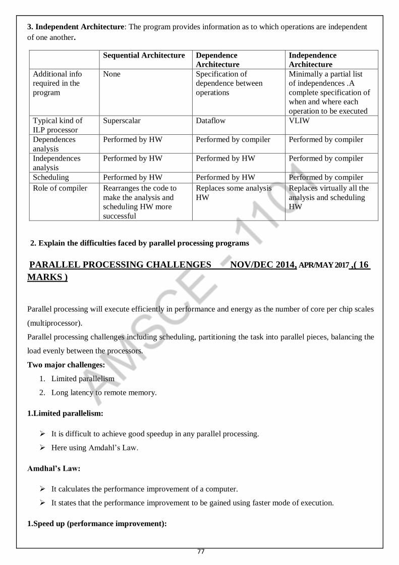
77
3. Independent Architecture: The program provides information as to which operations are independent
of one another.
Sequential Architecture Dependence
Architecture
Independence
Architecture
Additional info
required in the
program
None Specification of
dependence between
operations
Minimally a partial list
of independences .A
complete specification of
when and where each
operation to be executed
Typical kind of
ILP processor
Superscalar Dataflow VLIW
Dependences
analysis
Performed by HW Performed by compiler Performed by compiler
Independences
analysis
Performed by HW Performed by HW Performed by compiler
Scheduling Performed by HW Performed by HW Performed by compiler
Role of compiler Rearranges the code to
make the analysis and
scheduling HW more
successful
Replaces some analysis
HW
Replaces virtually all the
analysis and scheduling
HW
2. Explain the difficulties faced by parallel processing programs
PARALLEL PROCESSING CHALLENGES NOV/DEC 2014, APR/MAY 2017 ,( 16
MARKS )
Parallel processing will execute efficiently in performance and energy as the number of core per chip scales
(multiprocessor).
Parallel processing challenges including scheduling, partitioning the task into parallel pieces, balancing the
load evenly between the processors.
Two major challenges:
1. Limited parallelism
2. Long latency to remote memory.
1.Limited parallelism:
It is difficult to achieve good speedup in any parallel processing.
Here using Amdahl’s Law.
Amdhal’s Law:
It calculates the performance improvement of a computer.
It states that the performance improvement to be gained using faster mode of execution.
1.Speed up (performance improvement):
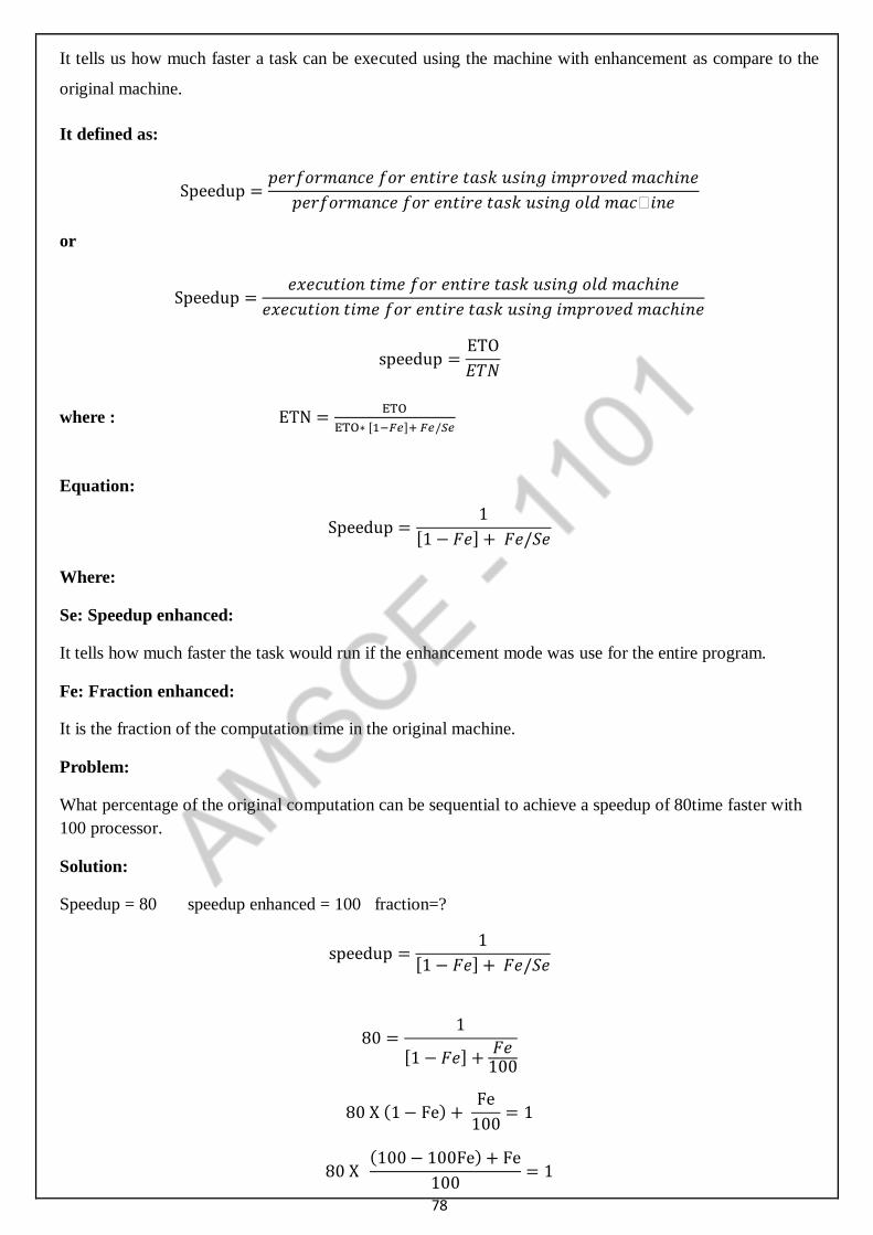
78
It tells us how much faster a task can be executed using the machine with enhancement as compare to the
original machine.
It defined as:
Speedup =𝑝𝑒𝑟𝑓𝑜𝑟𝑚𝑎𝑛𝑐𝑒 𝑓𝑜𝑟 𝑒𝑛𝑡𝑖𝑟𝑒 𝑡𝑎𝑠𝑘 𝑢𝑠𝑖𝑛𝑔 𝑖𝑚𝑝𝑟𝑜𝑣𝑒𝑑 𝑚𝑎𝑐ℎ𝑖𝑛𝑒
𝑝𝑒𝑟𝑓𝑜𝑟𝑚𝑎𝑛𝑐𝑒 𝑓𝑜𝑟 𝑒𝑛𝑡𝑖𝑟𝑒 𝑡𝑎𝑠𝑘 𝑢𝑠𝑖𝑛𝑔 𝑜𝑙𝑑 𝑚𝑎𝑐ℎ𝑖𝑛𝑒
or
Speedup =𝑒𝑥𝑒𝑐𝑢𝑡𝑖𝑜𝑛 𝑡𝑖𝑚𝑒 𝑓𝑜𝑟 𝑒𝑛𝑡𝑖𝑟𝑒 𝑡𝑎𝑠𝑘 𝑢𝑠𝑖𝑛𝑔 𝑜𝑙𝑑 𝑚𝑎𝑐ℎ𝑖𝑛𝑒
𝑒𝑥𝑒𝑐𝑢𝑡𝑖𝑜𝑛 𝑡𝑖𝑚𝑒 𝑓𝑜𝑟 𝑒𝑛𝑡𝑖𝑟𝑒 𝑡𝑎𝑠𝑘 𝑢𝑠𝑖𝑛𝑔 𝑖𝑚𝑝𝑟𝑜𝑣𝑒𝑑 𝑚𝑎𝑐ℎ𝑖𝑛𝑒
speedup =ETO
𝐸𝑇𝑁
where : ETN =ETO
ETO∗ [1−𝐹𝑒]+ 𝐹𝑒/𝑆𝑒
Equation:
Speedup =1
[1 − 𝐹𝑒] + 𝐹𝑒/𝑆𝑒
Where:
Se: Speedup enhanced:
It tells how much faster the task would run if the enhancement mode was use for the entire program.
Fe: Fraction enhanced:
It is the fraction of the computation time in the original machine.
Problem:
What percentage of the original computation can be sequential to achieve a speedup of 80time faster with
100 processor.
Solution:
Speedup = 80 speedup enhanced = 100 fraction=?
speedup =1
[1 − 𝐹𝑒] + 𝐹𝑒/𝑆𝑒
80 =1
[1 − 𝐹𝑒] +𝐹𝑒
100
80 X (1 − Fe) + Fe
100= 1
80 X (100 − 100Fe) + Fe
100= 1
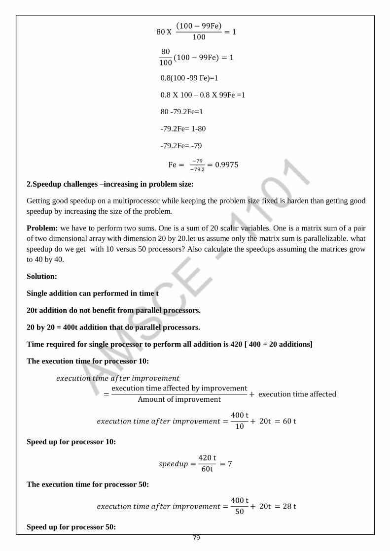
79
80 X (100 − 99Fe)
100= 1
80
100(100 − 99Fe) = 1
0.8(100 -99 Fe)=1
0.8 X 100 – 0.8 X 99Fe =1
80 -79.2Fe=1
-79.2Fe= 1-80
-79.2Fe= -79
Fe = −79
−79.2= 0.9975
2.Speedup challenges –increasing in problem size:
Getting good speedup on a multiprocessor while keeping the problem size fixed is harden than getting good
speedup by increasing the size of the problem.
Problem: we have to perform two sums. One is a sum of 20 scalar variables. One is a matrix sum of a pair
of two dimensional array with dimension 20 by 20.let us assume only the matrix sum is parallelizable. what
speedup do we get with 10 versus 50 processors? Also calculate the speedups assuming the matrices grow
to 40 by 40.
Solution:
Single addition can performed in time t
20t addition do not benefit from parallel processors.
20 by 20 = 400t addition that do parallel processors.
Time required for single processor to perform all addition is 420 [ 400 + 20 additions]
The execution time for processor 10:
𝑒𝑥𝑒𝑐𝑢𝑡𝑖𝑜𝑛 𝑡𝑖𝑚𝑒 𝑎𝑓𝑡𝑒𝑟 𝑖𝑚𝑝𝑟𝑜𝑣𝑒𝑚𝑒𝑛𝑡
=execution time affected by improvement
Amount of improvement+ execution time affected
𝑒𝑥𝑒𝑐𝑢𝑡𝑖𝑜𝑛 𝑡𝑖𝑚𝑒 𝑎𝑓𝑡𝑒𝑟 𝑖𝑚𝑝𝑟𝑜𝑣𝑒𝑚𝑒𝑛𝑡 =400 t
10+ 20t = 60 t
Speed up for processor 10:
𝑠𝑝𝑒𝑒𝑑𝑢𝑝 =420 t
60t = 7
The execution time for processor 50:
𝑒𝑥𝑒𝑐𝑢𝑡𝑖𝑜𝑛 𝑡𝑖𝑚𝑒 𝑎𝑓𝑡𝑒𝑟 𝑖𝑚𝑝𝑟𝑜𝑣𝑒𝑚𝑒𝑛𝑡 =400 t
50+ 20t = 28 t
Speed up for processor 50:
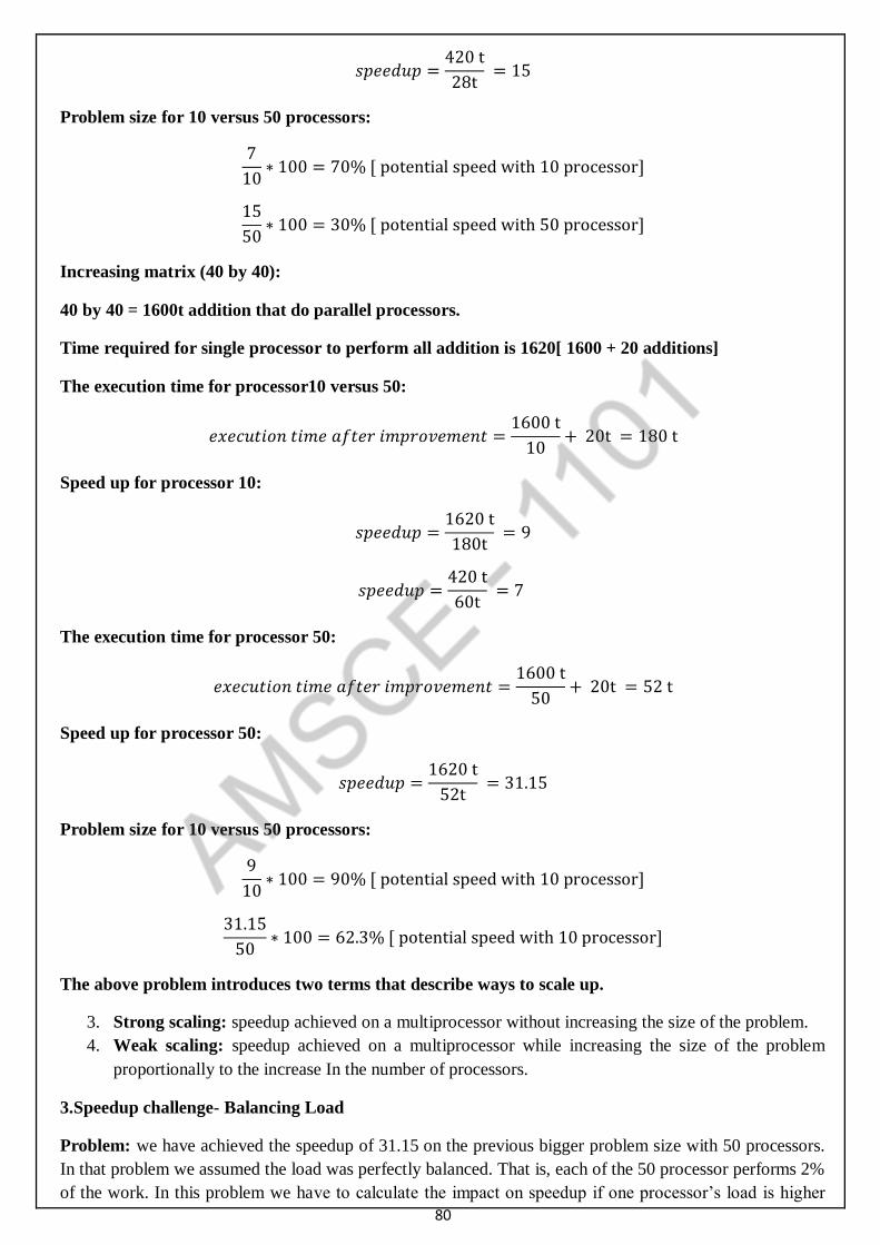
80
𝑠𝑝𝑒𝑒𝑑𝑢𝑝 =420 t
28t = 15
Problem size for 10 versus 50 processors:
7
10∗ 100 = 70% [ potential speed with 10 processor]
15
50∗ 100 = 30% [ potential speed with 50 processor]
Increasing matrix (40 by 40):
40 by 40 = 1600t addition that do parallel processors.
Time required for single processor to perform all addition is 1620[ 1600 + 20 additions]
The execution time for processor10 versus 50:
𝑒𝑥𝑒𝑐𝑢𝑡𝑖𝑜𝑛 𝑡𝑖𝑚𝑒 𝑎𝑓𝑡𝑒𝑟 𝑖𝑚𝑝𝑟𝑜𝑣𝑒𝑚𝑒𝑛𝑡 =1600 t
10+ 20t = 180 t
Speed up for processor 10:
𝑠𝑝𝑒𝑒𝑑𝑢𝑝 =1620 t
180t = 9
𝑠𝑝𝑒𝑒𝑑𝑢𝑝 =420 t
60t = 7
The execution time for processor 50:
𝑒𝑥𝑒𝑐𝑢𝑡𝑖𝑜𝑛 𝑡𝑖𝑚𝑒 𝑎𝑓𝑡𝑒𝑟 𝑖𝑚𝑝𝑟𝑜𝑣𝑒𝑚𝑒𝑛𝑡 =1600 t
50+ 20t = 52 t
Speed up for processor 50:
𝑠𝑝𝑒𝑒𝑑𝑢𝑝 =1620 t
52t = 31.15
Problem size for 10 versus 50 processors:
9
10∗ 100 = 90% [ potential speed with 10 processor]
31.15
50∗ 100 = 62.3% [ potential speed with 10 processor]
The above problem introduces two terms that describe ways to scale up.
3. Strong scaling: speedup achieved on a multiprocessor without increasing the size of the problem.
4. Weak scaling: speedup achieved on a multiprocessor while increasing the size of the problem
proportionally to the increase In the number of processors.
3.Speedup challenge- Balancing Load
Problem: we have achieved the speedup of 31.15 on the previous bigger problem size with 50 processors.
In that problem we assumed the load was perfectly balanced. That is, each of the 50 processor performs 2%
of the work. In this problem we have to calculate the impact on speedup if one processor’s load is higher
81
than all the rest. Calculate the impact on speedup if the hardest working processor’s load is 4% and
10%.Also calculate the utilization of the rest of the processors?
Solution: we are taking 50 processors [spilt 50 processors has 1 processor and 49 processors]
a. If one processor has 4 % of the parallel load, then it must do:
4% X 1600 = 64t addition
The other 49 processor will share the remaining 1536t addition [1600-64 =1536]
Calculate the execution time :
𝑒𝑥𝑒𝑐𝑢𝑡𝑖𝑜𝑛 𝑡𝑖𝑚𝑒 𝑎𝑓𝑡𝑒𝑟 𝑖𝑚𝑝𝑟𝑜𝑣𝑒𝑚𝑒𝑛𝑡 = max[1536 t
49 ,
64t
1 ] + 20t = 84 t
𝑠𝑝𝑒𝑒𝑑𝑢𝑝 =1620 t
84t = 19.29
The speedup drops from 31.15 to 19.29
Utilization of remaining 49 processors = 1536 t
49 = 31.35t
Thus we can say that the remaining 49 processors are utilized less than half the time as compared to 64t for
hardest working processor.
b. If one processor has 10 % of the parallel load, then it must do:
10% X 1600 = 160t addition
The other 49 processor will share the remaining 1440t addition [1600-160 =1440]
Calculate the execution time :
𝑒𝑥𝑒𝑐𝑢𝑡𝑖𝑜𝑛 𝑡𝑖𝑚𝑒 𝑎𝑓𝑡𝑒𝑟 𝑖𝑚𝑝𝑟𝑜𝑣𝑒𝑚𝑒𝑛𝑡 = max[1440 t
49 ,
160t
1 ] + 20t = 180 t
𝑠𝑝𝑒𝑒𝑑𝑢𝑝 =1620 t
180t = 9
The speedup drops from 31.15 to 9
Utilization of remaining 49 processors = 1440 t
49 = 29.39t
Thus we can say that the remaining 49 processors are utilized less than 20% of the time as compared to
160t for hardest working processor.
3. Explain in detail Flynn’s classification of parallel hardware
FLYNN’S CLASSIFICATION ( OR )
Discuss about SISD, MIMD, SIMD, SPMD and Vector systems
MAY/JUNE 2016, NOV/DEC 2015,
APR/MAY 2015, APR/MAY 2017,NOV/DEC
2019, APR/MAY 2016 ( 16 MARKS )
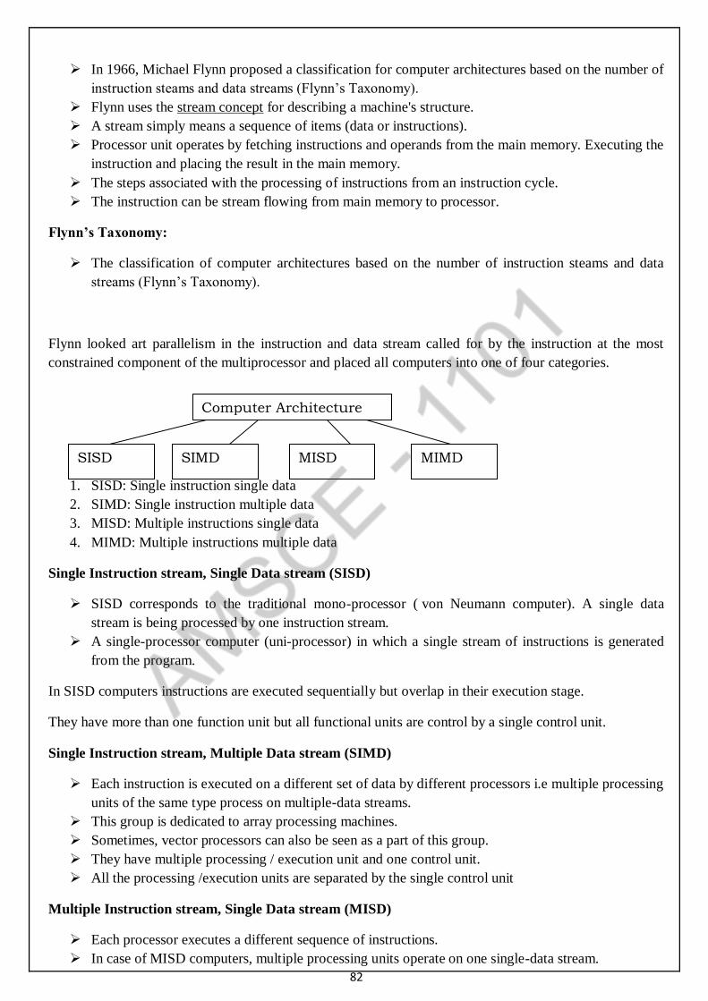
82
In 1966, Michael Flynn proposed a classification for computer architectures based on the number of
instruction steams and data streams (Flynn’s Taxonomy).
Flynn uses the stream concept for describing a machine's structure.
A stream simply means a sequence of items (data or instructions).
Processor unit operates by fetching instructions and operands from the main memory. Executing the
instruction and placing the result in the main memory.
The steps associated with the processing of instructions from an instruction cycle.
The instruction can be stream flowing from main memory to processor.
Flynn’s Taxonomy:
The classification of computer architectures based on the number of instruction steams and data
streams (Flynn’s Taxonomy).
Flynn looked art parallelism in the instruction and data stream called for by the instruction at the most
constrained component of the multiprocessor and placed all computers into one of four categories.
1. SISD: Single instruction single data
2. SIMD: Single instruction multiple data
3. MISD: Multiple instructions single data
4. MIMD: Multiple instructions multiple data
Single Instruction stream, Single Data stream (SISD)
SISD corresponds to the traditional mono-processor ( von Neumann computer). A single data
stream is being processed by one instruction stream.
A single-processor computer (uni-processor) in which a single stream of instructions is generated
from the program.
In SISD computers instructions are executed sequentially but overlap in their execution stage.
They have more than one function unit but all functional units are control by a single control unit.
Single Instruction stream, Multiple Data stream (SIMD)
Each instruction is executed on a different set of data by different processors i.e multiple processing
units of the same type process on multiple-data streams.
This group is dedicated to array processing machines.
Sometimes, vector processors can also be seen as a part of this group.
They have multiple processing / execution unit and one control unit.
All the processing /execution units are separated by the single control unit
Multiple Instruction stream, Single Data stream (MISD)
Each processor executes a different sequence of instructions.
In case of MISD computers, multiple processing units operate on one single-data stream.
Computer Architecture
SISD SIMD MISD MIMD

83
In practice, this kind of organization has never been used
Until recently no processor that really fits this category
– “Streaming” processors; each processor executes a kernel on a stream of data
– Maybe VLIW?
Multiple Instruction stream, Multiple Data stream (MIMD)
Each processor has a separate program.
An instruction stream is generated from each program.
Each instruction operates on different data.
This last machine type builds the group for the traditional multi-processors
More than one processor unit having the ability to execute the several program simultaneously.
In MIMD computer implies interactions among the multiple processor because all memory stream
are derived from the same data spare shared by all processors.
4. Explain in detail hardware Multithreading
HARDWARE MULTITHREADING TECHNIQUES APR/MAY 2016& NOV/DEC
2014 (8 MARKS ) , NOV/DEC 2015 , APR/MAY 2015, APR/MAY 2017, APR/MAY
2019 (16 MARKS )
Multi-threading
The ability of an operating system to execute different parts of a program, called threads,
simultaneously.
The programmer must carefully design the program in such a way that all the threads can run at the
same time without interfering with each other
The multithreading paradigm has become more popular as efforts to further exploit instruction level
parallelism have stalled.
Advantages of Multi-threading:
If a thread cannot use all the computing resources of the CPU, running another thread permits to not
leave these idle.
If several threads work on the same set of data, they can actually share its caching, leading to better
cache usage or synchronization on its values.
Hardware multithreading:
It allows multiple threads to share the functional units of a single processor in an overlapping fashion.
Increasing utilization of a processor by switching to another thread when one thread is stalled
Hardware Multithread done in 2 ways:
84
1. Fine-grained multi-threading :
Switches between threads on each instruction. causing the execution of multiple threads to be
interleaved
as the processor switches from one thread to the next, a thread that is currently stalled is skipped
over
CPU must be able to switch between threads at every clock cycle so that it needs extra hardware
support
Advantages
– less susceptible to stalling situations
– throughput costs can be hidden because stalls are often unnoticed
Disadvantages:
– slows down execution of each thread
– requires a switching process that does not cost any cycles
– this can be done at the expense of more hardware (we will require at a minimum a PC for
every thread)
2. Coarse-grained multi-threading:
switches between threads only when current thread is likely to stall for some time (e.g., level 2
cache miss)
the switching process can be more time consuming since we are not switching nearly as often and
therefore does not need extra hardware support
Advantages
– more natural flow for any given thread
– easier to implement switching process
– can take advantage of current processors to implement coarse-grained, but not fine-grained
Disadvantages: limited in its ability to overcome throughput losses because of short stalling situations
because the cost of starting the pipeline on a new thread is expensive (in comparison to fine-grained)
Illustration:
The following diagram illustration the differences in a processor’s ability to exploit the resources of
a superscalar for the following processor configuration
Issue Slots
Superscalar Coarse MT Fine MT SMT
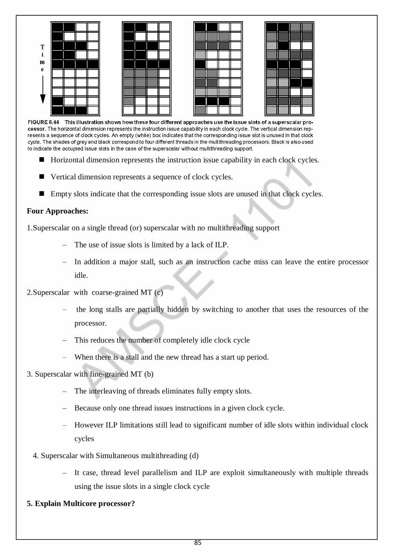
85
Horizontal dimension represents the instruction issue capability in each clock cycles.
Vertical dimension represents a sequence of clock cycles.
Empty slots indicate that the corresponding issue slots are unused in that clock cycles.
Four Approaches:
1.Superscalar on a single thread (or) superscalar with no multithreading support
– The use of issue slots is limited by a lack of ILP.
– In addition a major stall, such as an instruction cache miss can leave the entire processor
idle.
2.Superscalar with coarse-grained MT (c)
– the long stalls are partially hidden by switching to another that uses the resources of the
processor.
– This reduces the number of completely idle clock cycle
– When there is a stall and the new thread has a start up period.
3. Superscalar with fine-grained MT (b)
– The interleaving of threads eliminates fully empty slots.
– Because only one thread issues instructions in a given clock cycle.
– However ILP limitations still lead to significant number of idle slots within individual clock
cycles
4. Superscalar with Simultaneous multithreading (d)
– It case, thread level parallelism and ILP are exploit simultaneously with multiple threads
using the issue slots in a single clock cycle
5. Explain Multicore processor?
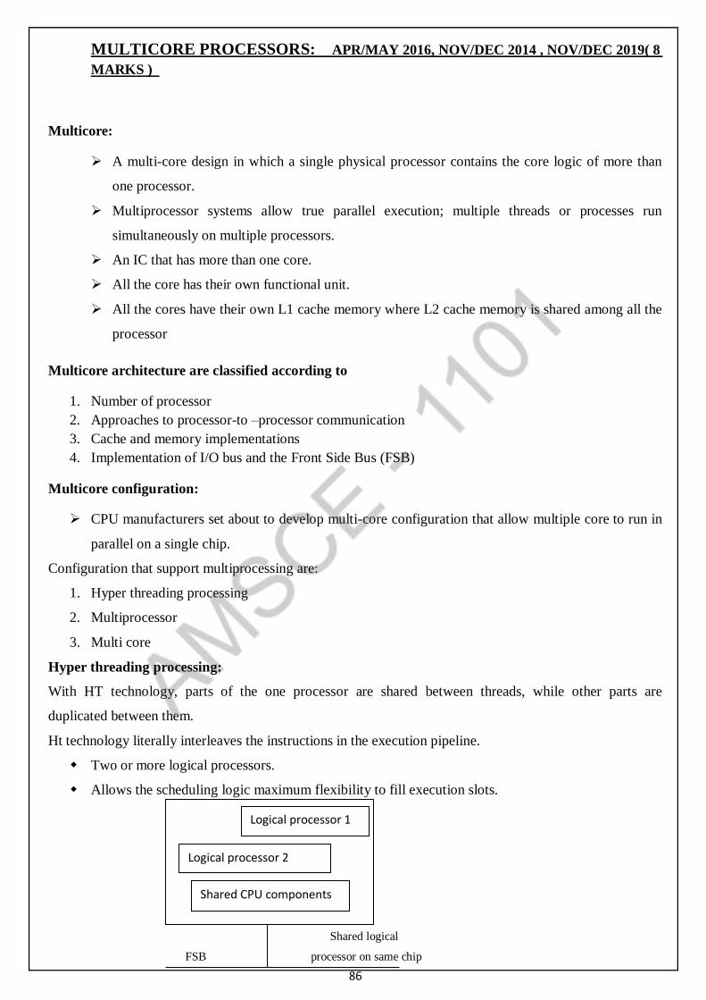
86
MULTICORE PROCESSORS: APR/MAY 2016, NOV/DEC 2014 , NOV/DEC 2019( 8
MARKS )
Multicore:
A multi-core design in which a single physical processor contains the core logic of more than
one processor.
Multiprocessor systems allow true parallel execution; multiple threads or processes run
simultaneously on multiple processors.
An IC that has more than one core.
All the core has their own functional unit.
All the cores have their own L1 cache memory where L2 cache memory is shared among all the
processor
Multicore architecture are classified according to
1. Number of processor
2. Approaches to processor-to –processor communication
3. Cache and memory implementations
4. Implementation of I/O bus and the Front Side Bus (FSB)
Multicore configuration:
CPU manufacturers set about to develop multi-core configuration that allow multiple core to run in
parallel on a single chip.
Configuration that support multiprocessing are:
1. Hyper threading processing
2. Multiprocessor
3. Multi core
Hyper threading processing:
With HT technology, parts of the one processor are shared between threads, while other parts are
duplicated between them.
Ht technology literally interleaves the instructions in the execution pipeline.
Two or more logical processors.
Allows the scheduling logic maximum flexibility to fill execution slots.
Shared logical
FSB processor on same chip
Logical processor 1
Logical processor 2
Shared CPU components
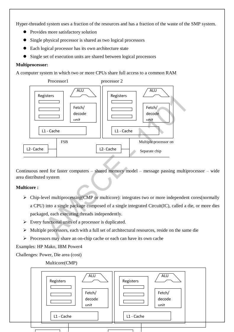
87
Hyper-threaded system uses a fraction of the resources and has a fraction of the waste of the SMP system.
Provides more satisfactory solution
Single physical processor is shared as two logical processors
Each logical processor has its own architecture state
Single set of execution units are shared between logical processors
Multiprocessor:
A computer system in which two or more CPUs share full access to a common RAM
Processor1 processor 2
FSB Multiple processor on
Separate chip
Continuous need for faster computers – shared memory model – message passing multiprocessor – wide
area distributed system
Multicore :
Chip-level multiprocessing(CMP or multicore): integrates two or more independent cores(normally
a CPU) into a single package composed of a single integrated Circuit(IC), called a die, or more dies
packaged, each executing threads independently.
Every functional units of a processor is duplicated.
Multiple processors, each with a full set of architectural resources, reside on the same die
Processors may share an on-chip cache or each can have its own cache
Examples: HP Mako, IBM Power4
Challenges: Power, Die area (cost)
Multicore(CMP)
ALU Registers
L1 - Cache
Fetch/
decode
unit
L2- Cache
ALU Registers
L1 - Cache
Fetch/
decode
unit
L2- Cache
ALU Registers
L1 - Cache
Fetch/
decode
unit
L2- Cache
ALU Registers
L1 - Cache
Fetch/
decode
unit
L2- Cache
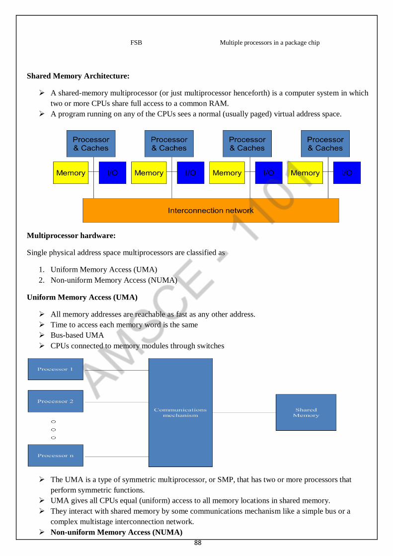
88
FSB Multiple processors in a package chip
Shared Memory Architecture:
A shared-memory multiprocessor (or just multiprocessor henceforth) is a computer system in which
two or more CPUs share full access to a common RAM.
A program running on any of the CPUs sees a normal (usually paged) virtual address space.
Multiprocessor hardware:
Single physical address space multiprocessors are classified as
1. Uniform Memory Access (UMA)
2. Non-uniform Memory Access (NUMA)
Uniform Memory Access (UMA)
All memory addresses are reachable as fast as any other address.
Time to access each memory word is the same
Bus-based UMA
CPUs connected to memory modules through switches
The UMA is a type of symmetric multiprocessor, or SMP, that has two or more processors that
perform symmetric functions.
UMA gives all CPUs equal (uniform) access to all memory locations in shared memory.
They interact with shared memory by some communications mechanism like a simple bus or a
complex multistage interconnection network.
Non-uniform Memory Access (NUMA)
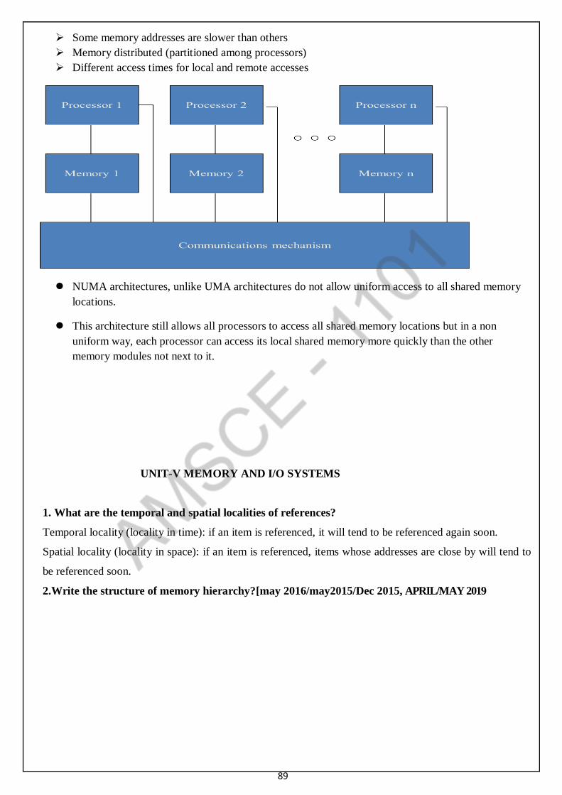
89
Some memory addresses are slower than others
Memory distributed (partitioned among processors)
Different access times for local and remote accesses
NUMA architectures, unlike UMA architectures do not allow uniform access to all shared memory
locations.
This architecture still allows all processors to access all shared memory locations but in a non
uniform way, each processor can access its local shared memory more quickly than the other
memory modules not next to it.
UNIT-V MEMORY AND I/O SYSTEMS
1. What are the temporal and spatial localities of references?
Temporal locality (locality in time): if an item is referenced, it will tend to be referenced again soon.
Spatial locality (locality in space): if an item is referenced, items whose addresses are close by will tend to
be referenced soon.
2.Write the structure of memory hierarchy?[may 2016/may2015/Dec 2015, APRIL/MAY 2019
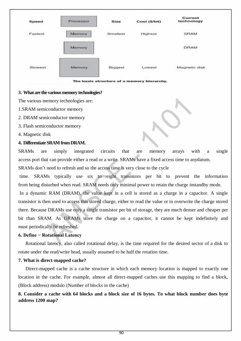
90
3. What are the various memory technologies?
The various memory technologies are:
1.SRAM semiconductor memory
2. DRAM semiconductor memory
3. Flash semiconductor memory
4. Magnetic disk
4. Differentiate SRAM from DRAM.
SRAMs are simply integrated circuits that are memory arrays with a single
access port that can provide either a read or a write. SRAMs have a fixed access time to anydatum.
SRAMs don’t need to refresh and so the access time is very close to the cycle
time. SRAMs typically use six to eight transistors per bit to prevent the information
from being disturbed when read. SRAM needs only minimal power to retain the charge instandby mode.
In a dynamic RAM (DRAM), the value kept in a cell is stored as a charge in a capacitor. A single
transistor is then used to access this stored charge, either to read the value or to overwrite the charge stored
there. Because DRAMs use only a single transistor per bit of storage, they are much denser and cheaper per
bit than SRAM. As DRAMs store the charge on a capacitor, it cannot be kept indefinitely and
must periodically be refreshed.
6. Define − Rotational Latency
Rotational latency, also called rotational delay, is the time required for the desired sector of a disk to
rotate under the read/write head, usually assumed to be half the rotation time.
7. What is direct-mapped cache?
Direct-mapped cache is a cache structure in which each memory location is mapped to exactly one
location in the cache. For example, almost all direct-mapped caches use this mapping to find a block,
(Block address) modulo (Number of blocks in the cache)
8. Consider a cache with 64 blocks and a block size of 16 bytes. To what block number does byte
address 1200 map?
91
9. How many total bits are required for a direct-mapped cache with 16 KiB ofdata and 4-word blocks, assuming a
32-bit address?APRIL/MAY 2019
10. What are the writing strategies in cache memory?
Write-through is a scheme in which writes always update both the cache and the next lower level of
the memory hierarchy, ensuring that data is always consistent between the two. Write-back is a scheme that
handles writes by updating values only to the block in the cache, then writing the modified block to the
lower level of the hierarchy when the block is replaced.
11. What are the steps to be taken in an instruction cache miss?
The steps to be taken on an instruction cache miss are
92
1. Send the original PC value (current PC – 4) to the memory.
2. Instruct main memory to perform a read and wait for the memory to complete its access.
3. Write the cache entry, putting the data from memory in the data portion of
the entry, writing the upper bits of the address (from the ALU) into the tag field, and turning the valid bit
on.
4. Restart the instruction execution at the first step, which will re fetch the instruction, this time finding it in
the cache.
12. Define – AMAT
Average memory access time is the average time to access memory considering both hits and misses and
the frequency of different accesses. It is equal to the following:
13. What are the various block placement schemes in cache memory?
Direct-mapped cache is a cache structure in which each memory location is mapped to exactly one location
in the cache.
Fully associative cache is a cache structure in which a block can be placed in any location in the cache.
Set-associative cache is a cache that has a fixed number of locations (at least two) where each block can be
placed.
14.Define – MTTF and AFR
Reliability is a measure of the continuous service accomplishment or, equivalently, of the time to failure
from a reference point. Hence, mean time to failure(MTTF) is a reliability measure. A related term is
annual failure rate (AFR), which is just the percentage of devices that would be expected to fail in a year
for a given MTTF.
15. Define – Availability
Availability is then a measure of service accomplishment with respect to the alternation between the two
states of accomplishment and interruption. Availability is statistically quantified as
16. What are the three ways to improve MTTF?
The three ways to improve MTTF are:1. Fault avoidance: Preventing fault occurrence by construction.2.
Fault tolerance: Using redundancy to allow the service to comply with the service specification despite
faults occurring.3. Fault forecasting: Predicting the presence and creation of faults, allowing the component
to be replaced before it fails.
17. Define – TLB
Translation-Look aside Buffer (TLB) is a cache that keeps track of recently used address mappings to try to
avoid an access to the page table.
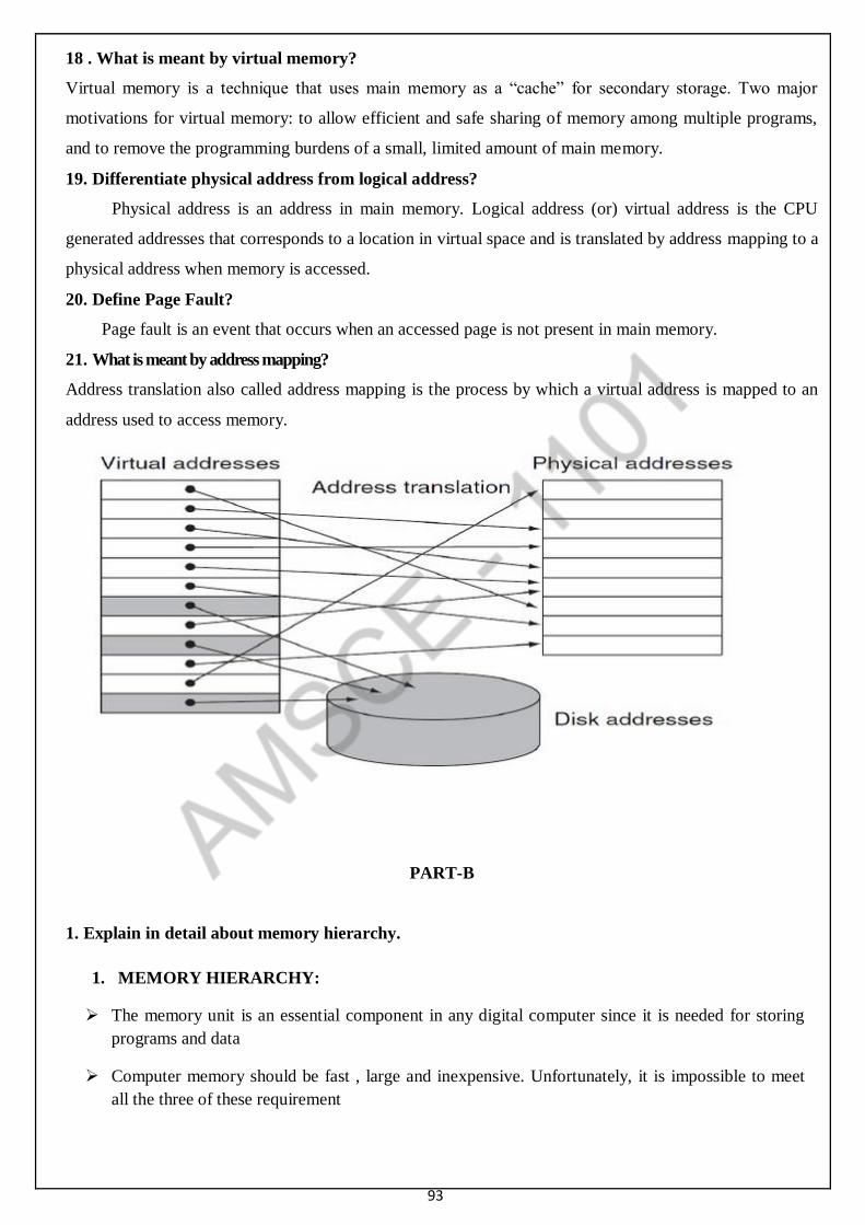
93
18 . What is meant by virtual memory?
Virtual memory is a technique that uses main memory as a “cache” for secondary storage. Two major
motivations for virtual memory: to allow efficient and safe sharing of memory among multiple programs,
and to remove the programming burdens of a small, limited amount of main memory.
19. Differentiate physical address from logical address?
Physical address is an address in main memory. Logical address (or) virtual address is the CPU
generated addresses that corresponds to a location in virtual space and is translated by address mapping to a
physical address when memory is accessed.
20. Define Page Fault?
Page fault is an event that occurs when an accessed page is not present in main memory.
21. What is meant by address mapping?
Address translation also called address mapping is the process by which a virtual address is mapped to an
address used to access memory.
PART-B
1. Explain in detail about memory hierarchy.
1. MEMORY HIERARCHY:
The memory unit is an essential component in any digital computer since it is needed for storing
programs and data
Computer memory should be fast , large and inexpensive. Unfortunately, it is impossible to meet
all the three of these requirement
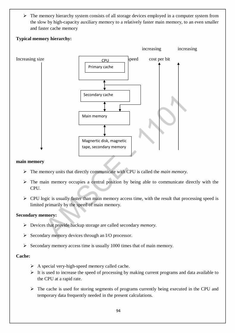
94
The memory hierarchy system consists of all storage devices employed in a computer system from
the slow by high-capacity auxiliary memory to a relatively faster main memory, to an even smaller
and faster cache memory
Typical memory hierarchy:
increasing increasing
Increasing size speed cost per bit
main memory
The memory units that directly communicate with CPU is called the main memory.
The main memory occupies a central position by being able to communicate directly with the
CPU.
CPU logic is usually faster than main memory access time, with the result that processing speed is
limited primarily by the speed of main memory.
Secondary memory:
Devices that provide backup storage are called secondary memory.
Secondary memory devices through an I/O processor.
Secondary memory access time is usually 1000 times that of main memory.
Cache:
A special very-high-speed memory called cache.
It is used to increase the speed of processing by making current programs and data available to
the CPU at a rapid rate.
The cache is used for storing segments of programs currently being executed in the CPU and
temporary data frequently needed in the present calculations.
CPU
Primary cache
Secondary cache
Main memory
Magnertic disk, magnetic
tape, secondary memory
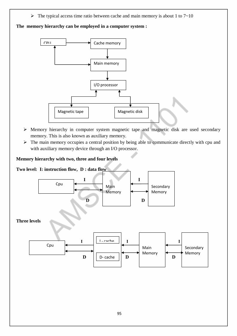
95
The typical access time ratio between cache and main memory is about 1 to 7~10
The memory hierarchy can be employed in a computer system :
Memory hierarchy in computer system magnetic tape and magnetic disk are used secondary
memory. This is also known as auxiliary memory.
The main memory occupies a central position by being able to communicate directly with cpu and
with auxiliary memory device through an I/O processor.
Memory hierarchy with two, three and four levels
Two level: I: instruction flow, D : data flow
I I
D D
Three levels
I I I
D D D
CPU Cache memory
Main memory
I/O processor
Magnetic tape Magnetic disk
Cpu
Main Memory
Secondary Memory
Cpu
Main Memory
Secondary Memory
I - cache
D- cache
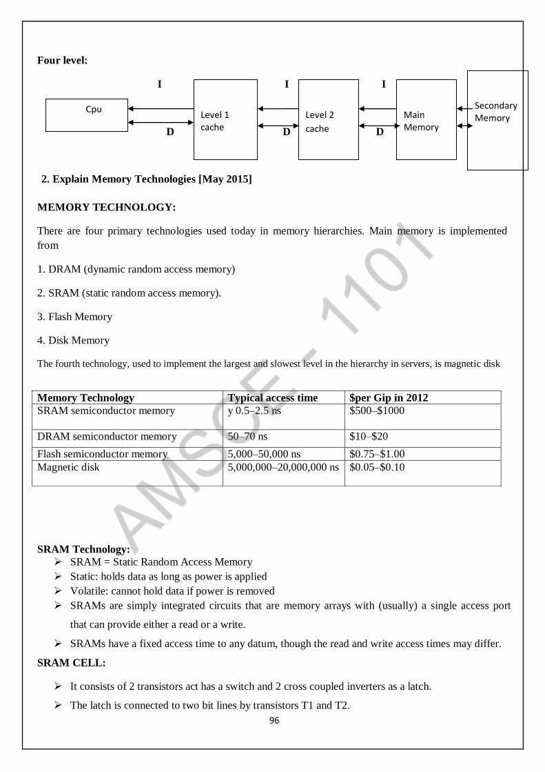
96
Four level:
I I I
D D D
2. Explain Memory Technologies [May 2015]
MEMORY TECHNOLOGY:
There are four primary technologies used today in memory hierarchies. Main memory is implemented
from
1. DRAM (dynamic random access memory)
2. SRAM (static random access memory).
3. Flash Memory
4. Disk Memory
The fourth technology, used to implement the largest and slowest level in the hierarchy in servers, is magnetic disk
mory technology Typical access time $ per Gi2
SRAM Technology:
SRAM = Static Random Access Memory
Static: holds data as long as power is applied
Volatile: cannot hold data if power is removed
SRAMs are simply integrated circuits that are memory arrays with (usually) a single access port
that can provide either a read or a write.
SRAMs have a fixed access time to any datum, though the read and write access times may differ.
SRAM CELL:
It consists of 2 transistors act has a switch and 2 cross coupled inverters as a latch.
The latch is connected to two bit lines by transistors T1 and T2.
Memory Technology Typical access time $per Gip in 2012
SRAM semiconductor memory
y 0.5–2.5 ns $500–$1000
DRAM semiconductor memory 50–70 ns $10–$20
Flash semiconductor memory 5,000–50,000 ns $0.75–$1.00
Magnetic disk 5,000,000–20,000,000 ns $0.05–$0.10
Cpu
Level 1 cache
Level 2
cache
Main Memory
Secondary Memory
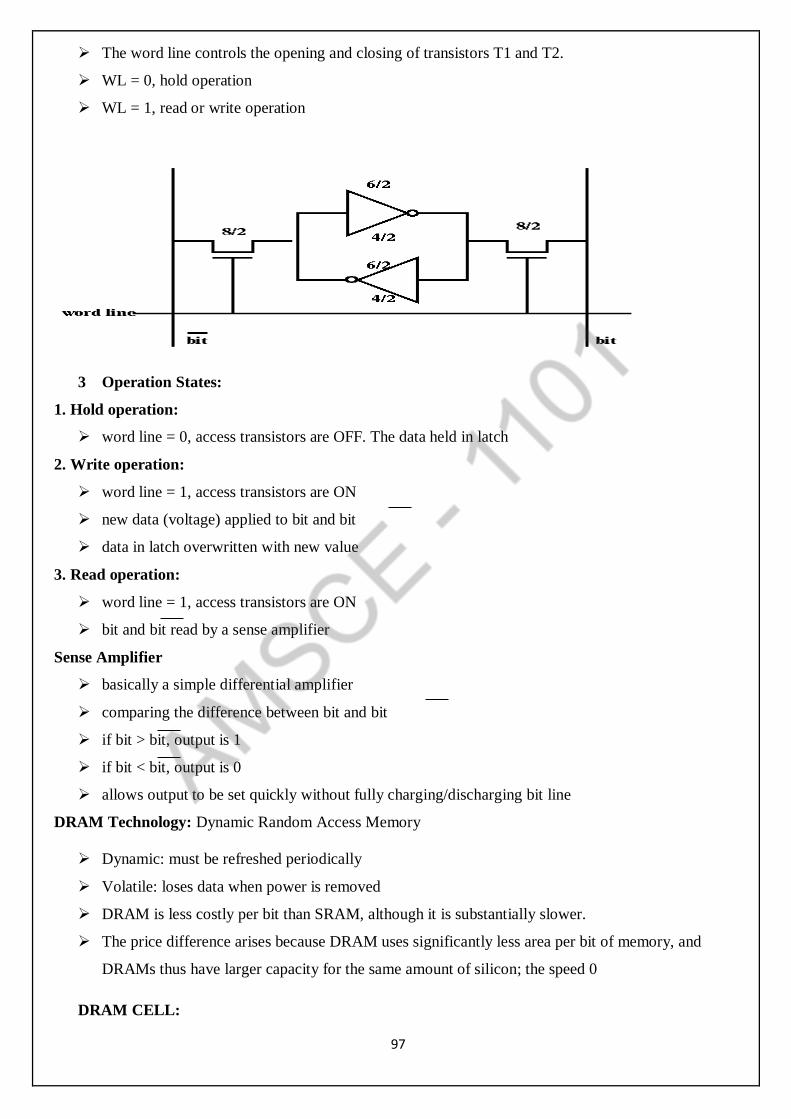
97
The word line controls the opening and closing of transistors T1 and T2.
WL = 0, hold operation
WL = 1, read or write operation
3 Operation States:
1. Hold operation:
word line = 0, access transistors are OFF. The data held in latch
2. Write operation:
word line = 1, access transistors are ON
new data (voltage) applied to bit and bit
data in latch overwritten with new value
3. Read operation:
word line = 1, access transistors are ON
bit and bit read by a sense amplifier
Sense Amplifier
basically a simple differential amplifier
comparing the difference between bit and bit
if bit > bit, output is 1
if bit < bit, output is 0
allows output to be set quickly without fully charging/discharging bit line
DRAM Technology: Dynamic Random Access Memory
Dynamic: must be refreshed periodically
Volatile: loses data when power is removed
DRAM is less costly per bit than SRAM, although it is substantially slower.
The price difference arises because DRAM uses significantly less area per bit of memory, and
DRAMs thus have larger capacity for the same amount of silicon; the speed 0
DRAM CELL:
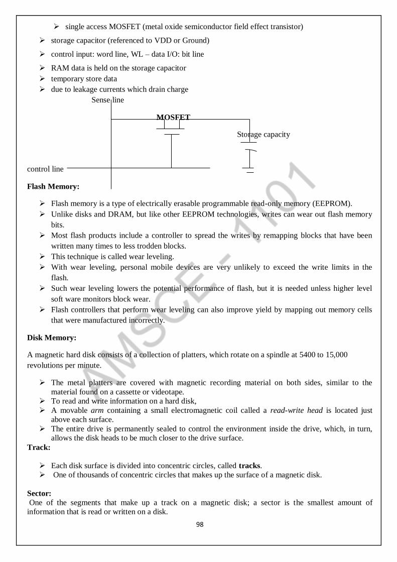
98
single access MOSFET (metal oxide semiconductor field effect transistor)
storage capacitor (referenced to VDD or Ground)
control input: word line, WL – data I/O: bit line
RAM data is held on the storage capacitor
temporary store data
due to leakage currents which drain charge
Sense line
MOSFET
Storage capacity
control line
Flash Memory:
Flash memory is a type of electrically erasable programmable read-only memory (EEPROM).
Unlike disks and DRAM, but like other EEPROM technologies, writes can wear out flash memory
bits.
Most flash products include a controller to spread the writes by remapping blocks that have been
written many times to less trodden blocks.
This technique is called wear leveling.
With wear leveling, personal mobile devices are very unlikely to exceed the write limits in the
flash.
Such wear leveling lowers the potential performance of flash, but it is needed unless higher level
soft ware monitors block wear.
Flash controllers that perform wear leveling can also improve yield by mapping out memory cells
that were manufactured incorrectly.
Disk Memory:
A magnetic hard disk consists of a collection of platters, which rotate on a spindle at 5400 to 15,000
revolutions per minute.
The metal platters are covered with magnetic recording material on both sides, similar to the
material found on a cassette or videotape.
To read and write information on a hard disk,
A movable arm containing a small electromagnetic coil called a read-write head is located just
above each surface.
The entire drive is permanently sealed to control the environment inside the drive, which, in turn,
allows the disk heads to be much closer to the drive surface.
Track:
Each disk surface is divided into concentric circles, called tracks.
One of thousands of concentric circles that makes up the surface of a magnetic disk.
Sector:
One of the segments that make up a track on a magnetic disk; a sector is the smallest amount of
information that is read or written on a disk.
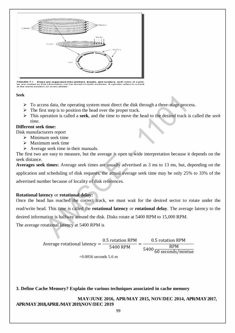
99
Seek
To access data, the operating system must direct the disk through a three-stage process.
The first step is to position the head over the proper track.
This operation is called a seek, and the time to move the head to the desired track is called the seek
time.
Different seek time:
Disk manufacturers report
Minimum seek time
Maximum seek time
Average seek time in their manuals.
The first two are easy to measure, but the average is open to wide interpretation because it depends on the
seek distance.
Averages seek times: Average seek times are usually advertised as 3 ms to 13 ms, but, depending on the
application and scheduling of disk requests, the actual average seek time may be only 25% to 33% of the
advertised number because of locality of disk references.
Rotational latency or rotational delay:
Once the head has reached the correct track, we must wait for the desired sector to rotate under the
read/write head. This time is called the rotational latency or rotational delay. The average latency to the
desired information is halfway around the disk. Disks rotate at 5400 RPM to 15,000 RPM.
The average rotational latency at 5400 RPM is
Average rotational latency =0.5 rotation RPM
5400 RPM=
0.5 rotation RPM
5400RPM
60 seconds/mintue
=0.0056 seconds 5.6 m
3. Define Cache Memory? Explain the various techniques associated in cache memory
MAY/JUNE 2016, APR/MAY 2015, NOV/DEC 2014, APR/MAY 2017,
APR/MAY 2018,APRIL/MAY 2019,NOV/DEC 2019
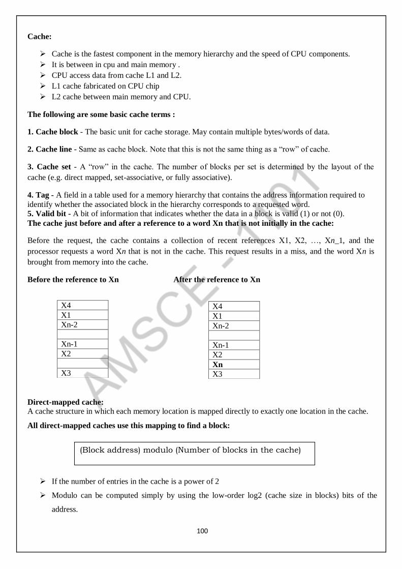
100
Cache:
Cache is the fastest component in the memory hierarchy and the speed of CPU components.
It is between in cpu and main memory .
CPU access data from cache L1 and L2.
L1 cache fabricated on CPU chip
L2 cache between main memory and CPU.
The following are some basic cache terms :
1. Cache block - The basic unit for cache storage. May contain multiple bytes/words of data.
2. Cache line - Same as cache block. Note that this is not the same thing as a “row” of cache.
3. Cache set - A “row” in the cache. The number of blocks per set is determined by the layout of the
cache (e.g. direct mapped, set-associative, or fully associative).
4. Tag - A field in a table used for a memory hierarchy that contains the address information required to
identify whether the associated block in the hierarchy corresponds to a requested word.
5. Valid bit - A bit of information that indicates whether the data in a block is valid (1) or not (0).
The cache just before and after a reference to a word Xn that is not initially in the cache:
Before the request, the cache contains a collection of recent references X1, X2, …, Xn_1, and the
processor requests a word Xn that is not in the cache. This request results in a miss, and the word Xn is
brought from memory into the cache.
Before the reference to Xn After the reference to Xn
Direct-mapped cache:
A cache structure in which each memory location is mapped directly to exactly one location in the cache.
All direct-mapped caches use this mapping to find a block:
If the number of entries in the cache is a power of 2
Modulo can be computed simply by using the low-order log2 (cache size in blocks) bits of the
address.
X4
X1
Xn-2
Xn-1
X2
Xn
X3
X4
X1
Xn-2
Xn-1
X2
X3
(Block address) modulo (Number of blocks in the cache)
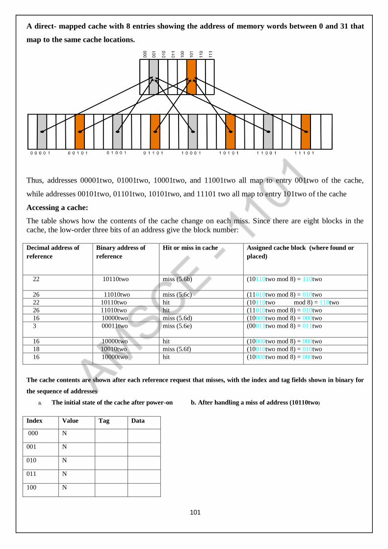
101
A direct- mapped cache with 8 entries showing the address of memory words between 0 and 31 that
map to the same cache locations.
Thus, addresses 00001two, 01001two, 10001two, and 11001two all map to entry 001two of the cache,
while addresses 00101two, 01101two, 10101two, and 11101 two all map to entry 101two of the cache
Accessing a cache:
The table shows how the contents of the cache change on each miss. Since there are eight blocks in the
cache, the low-order three bits of an address give the block number:
Decimal address of
reference
Binary address of
reference
Hit or miss in cache
Assigned cache block (where found or
placed)
22 10110two miss (5.6b) (10110two mod 8) = 110two
26 11010two miss (5.6c) (11010two mod 8) = 010two
22 10110two hit (10110two mod 8) = 110two
26 11010two hit (11010two mod 8) = 010two
16 10000two miss (5.6d) (10000two mod 8) = 000two
3 00011two
miss (5.6e)
(00011two mod 8) = 011two
16 10000two hit (10000two mod 8) = 000two
18 10010two miss (5.6f) (10010two mod 8) = 010two
16 10000two hit (10000two mod 8) = 000two
The cache contents are shown after each reference request that misses, with the index and tag fields shown in binary for
the sequence of addresses
a. The initial state of the cache after power-on b. After handling a miss of address (10110two)
Index Value Tag Data
000 N
001 N
010 N
011 N
100 N
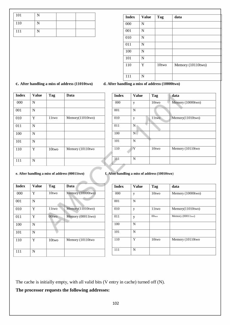
102
c. After handling a miss of address (11010two) d. After handling a miss of address (10000two)
e. After handling a miss of address (00011two) f. After handling a miss of address (10010two)
The cache is initially empty, with all valid bits (V entry in cache) turned off (N).
The processor requests the following addresses:
101 N
110 N
111 N
Index Value Tag data
000 N
001 N
010 N
011 N
100 N
101 N
110 Y 10two
Memory (10110two)
111 N
Index Value Tag Data
000 N
001 N
010 Y 11two Memory(11010two)
011 N
100 N
101 N
110 Y 10two
Memory (10110two
111 N
Index Value Tag data
000 y 10two Memory (10000two)
001 N
010 y 11two Memory(11010two)
011 N
100 N
101 N
110 Y 10two
Memory (10110two
111 N
Index Value Tag Data
000 Y 10two Memory (10000two)
001 N
010 Y 11two Memory(11010two)
011 Y 00two Memory (00011two)
100 N
101 N
110 Y 10two
Memory (10110two
111 N
Index Value Tag data
000 y 10two Memory (10000two)
001 N
010 y 11two Memory(11010two)
011 y 00two Memory (00011two)
100 N
101 N
110 Y 10two
Memory (10110two
111 N
103
10110two (miss), 11010two (miss), 10110two (hit), 11010two (hit), 10000two (miss),00011two (miss),
10000two (hit), 10010two (miss), and 10000two (hit).
The figures show the cache contents after each miss in the sequence has been handled. When address
10010two (18) is referenced, the entry for address 11010two (26) must be replaced, and a reference to
11010two will cause a subsequent miss.
cache for each possible address:
The low-order bits of an address can be used to find the unique cache entry to which the address could
map.
Figure shows how a referenced address is divided into
A tag field: which is used to compare with the value of the tag field of the cache.
A cache index: which is used to select the block 32 bit address.
■ The cache size is 2n blocks, so n bits are used for the index
■ The block size is 2m words (2m+2 bytes), so m bits are used for the word within the block, and two bits
are used for the byte part of the address the size of the tag field is
32 - (n + m + 2).
The total number of bits in a direct-mapped cache is
2n * (block size + tag size + valid field size).
This cache holds 1024 words or 4 KiB. We assume 32-bit addresses in this chapter.
The tag from the cache is compared against the upper portion of the address to determine whether
the entry in the cache corresponds to the requested address.
Because the cache has 210 (or 1024) words and a block size of one word, 10 bits are used to index
the cache, leaving 32 −10 − 2 = 20 bits to be compared against the tag.
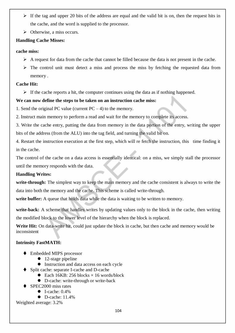
104
If the tag and upper 20 bits of the address are equal and the valid bit is on, then the request hits in
the cache, and the word is supplied to the processor.
Otherwise, a miss occurs.
Handling Cache Misses:
cache miss:
A request for data from the cache that cannot be filled because the data is not present in the cache.
The control unit must detect a miss and process the miss by fetching the requested data from
memory .
Cache Hit:
If the cache reports a hit, the computer continues using the data as if nothing happened.
We can now define the steps to be taken on an instruction cache miss:
1. Send the original PC value (current PC – 4) to the memory.
2. Instruct main memory to perform a read and wait for the memory to complete its access.
3. Write the cache entry, putting the data from memory in the data portion of the entry, writing the upper
bits of the address (from the ALU) into the tag field, and turning the valid bit on.
4. Restart the instruction execution at the first step, which will re fetch the instruction, this time finding it
in the cache.
The control of the cache on a data access is essentially identical: on a miss, we simply stall the processor
until the memory responds with the data.
Handling Writes:
write-through: The simplest way to keep the main memory and the cache consistent is always to write the
data into both the memory and the cache. This scheme is called write-through.
write buffer: A queue that holds data while the data is waiting to be written to memory.
write-back: A scheme that handles writes by updating values only to the block in the cache, then writing
the modified block to the lower level of the hierarchy when the block is replaced.
Write Hit: On data-write hit, could just update the block in cache, but then cache and memory would be
inconsistent
Intrinsity FastMATH:
Embedded MIPS processor
12-stage pipeline
Instruction and data access on each cycle
Split cache: separate I-cache and D-cache
Each 16KB: 256 blocks × 16 words/block
D-cache: write-through or write-back
SPEC2000 miss rates
I-cache: 0.4%
D-cache: 11.4%
Weighted average: 3.2%
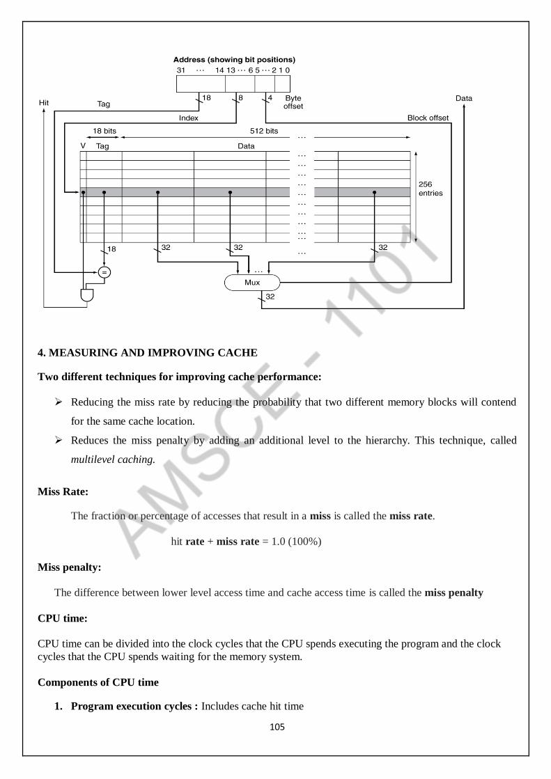
105
4. MEASURING AND IMPROVING CACHE
Two different techniques for improving cache performance:
Reducing the miss rate by reducing the probability that two different memory blocks will contend
for the same cache location.
Reduces the miss penalty by adding an additional level to the hierarchy. This technique, called
multilevel caching.
Miss Rate:
The fraction or percentage of accesses that result in a miss is called the miss rate.
hit rate + miss rate = 1.0 (100%)
Miss penalty:
The difference between lower level access time and cache access time is called the miss penalty
CPU time:
CPU time can be divided into the clock cycles that the CPU spends executing the program and the clock
cycles that the CPU spends waiting for the memory system.
Components of CPU time
1. Program execution cycles : Includes cache hit time

106
CPU time = (CPU execution clock cycles + Memory-stall clock cycles) X Clock cycle time
2. Memory stall cycles :
Defined as the sum of the stall cycles coming from reads plus those coming from writes.
Memory-stall clock cycles = (Read-stall cycles + Write-stall cycles)
Read stall cycles =Reads
program𝑋 𝑋𝑋𝑋𝑋 𝑋𝑋𝑋𝑋 𝑋𝑋𝑋𝑋 𝑋 𝑋𝑋𝑋𝑋 𝑋𝑋𝑋𝑋 𝑋𝑋𝑋𝑋𝑋𝑋𝑋
write stall cycles =writes
program𝑋 𝑋𝑋𝑋𝑋𝑋 𝑋𝑋𝑋𝑋 𝑋𝑋𝑋𝑋 𝑋 𝑋𝑋𝑋𝑋𝑋 𝑋𝑋𝑋𝑋 𝑋𝑋𝑋𝑋𝑋𝑋𝑋
Memory stall cycles =Memory accesses
program𝑋 𝑋𝑋𝑋𝑋 𝑋𝑋𝑋𝑋 𝑋 𝑋𝑋𝑋𝑋 𝑋𝑋𝑋𝑋𝑋𝑋𝑋
We can also factor this as
Memory stall cycles =Instructions
program𝑋
Misses
instruction 𝑋 𝑋𝑋𝑋𝑋 𝑋𝑋𝑋𝑋𝑋𝑋𝑋
Problem:
Assume the miss rate of an instruction cache is 2% and the miss rate of the data cache is 4%. If a processor
has a CPI of 2 without any memory stalls and the miss penalty is 100 cycles for all misses, determine how
much faster a processor would run with a perfect cache that never missed. Assume the frequency of all
loads and stores is 36%.
Given
I-cache miss rate = 2% [0.02]
D-cache miss rate = 4% [0.04]
Miss penalty = 100 cycles
Base CPI (ideal cache) = 2
Load & stores are 36% of instructions
Miss cycles per instruction
I-cache: Miss rate x miss penalty
0.02 × 100 = 2
D-cache: Miss rate x miss penalty
0.36 × 0.04 × 100 = 1.44
Actual CPI is
Memory stall+ I-cache + D-cache
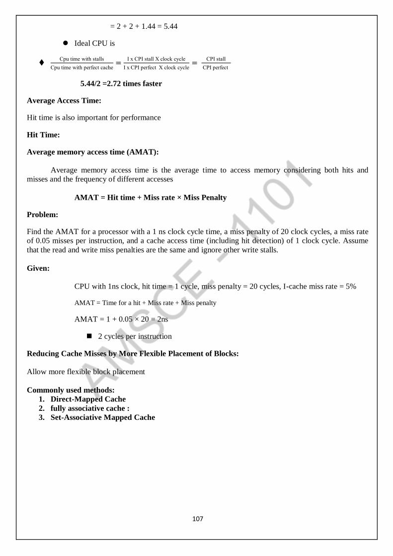
107
= 2 + 2 + 1.44 = 5.44
Ideal CPU is
Cpu time with stalls
Cpu time with perfect cache=
I x CPI stall X clock cycle
I x CPI perfect X clock cycle=
CPI stall
CPI perfect
5.44/2 =2.72 times faster
Average Access Time:
Hit time is also important for performance
Hit Time:
Average memory access time (AMAT):
Average memory access time is the average time to access memory considering both hits and
misses and the frequency of different accesses
AMAT = Hit time + Miss rate × Miss Penalty
Problem:
Find the AMAT for a processor with a 1 ns clock cycle time, a miss penalty of 20 clock cycles, a miss rate
of 0.05 misses per instruction, and a cache access time (including hit detection) of 1 clock cycle. Assume
that the read and write miss penalties are the same and ignore other write stalls.
Given:
CPU with 1ns clock, hit time = 1 cycle, miss penalty = 20 cycles, I-cache miss rate = 5%
AMAT = Time for a hit + Miss rate + Miss penalty
AMAT = 1 + 0.05 × 20 = 2ns
2 cycles per instruction
Reducing Cache Misses by More Flexible Placement of Blocks:
Allow more flexible block placement
Commonly used methods:
1. Direct-Mapped Cache
2. fully associative cache :
3. Set-Associative Mapped Cache
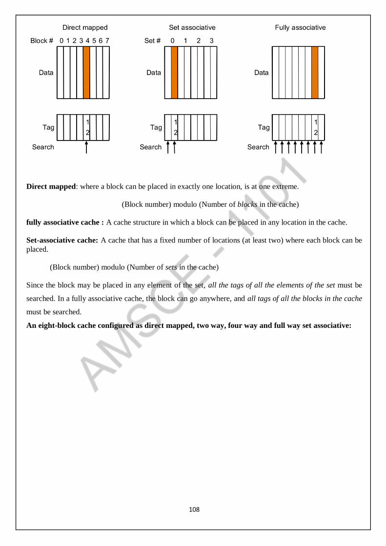
108
Direct mapped: where a block can be placed in exactly one location, is at one extreme.
(Block number) modulo (Number of blocks in the cache)
fully associative cache : A cache structure in which a block can be placed in any location in the cache.
Set-associative cache: A cache that has a fixed number of locations (at least two) where each block can be
placed.
(Block number) modulo (Number of sets in the cache)
Since the block may be placed in any element of the set, all the tags of all the elements of the set must be
searched. In a fully associative cache, the block can go anywhere, and all tags of all the blocks in the cache
must be searched.
An eight-block cache configured as direct mapped, two way, four way and full way set associative:
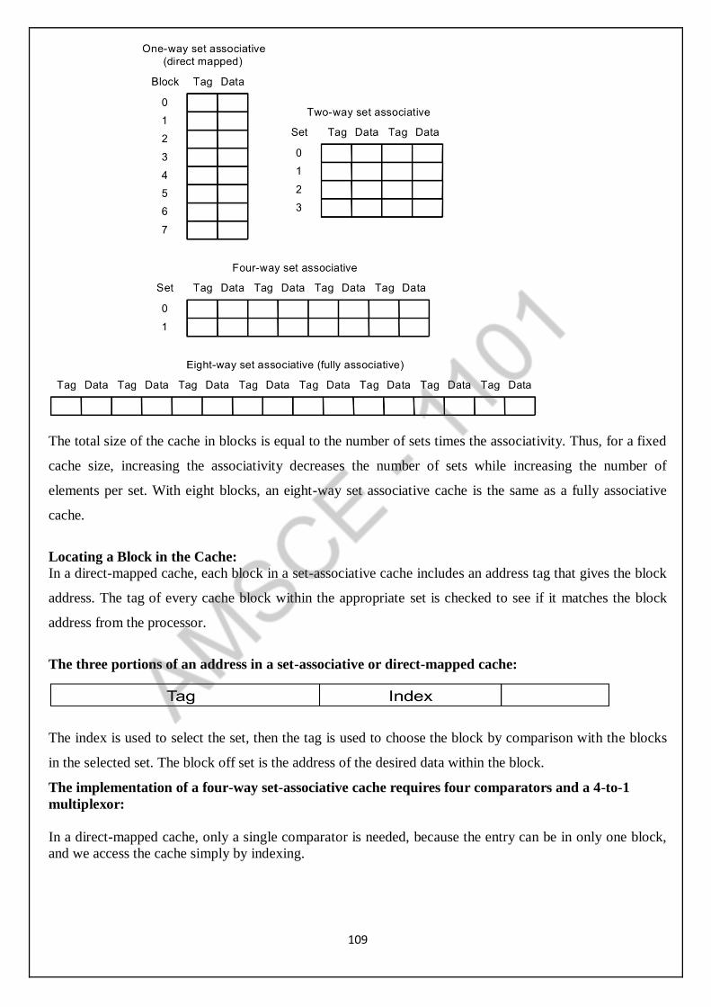
109
The total size of the cache in blocks is equal to the number of sets times the associativity. Thus, for a fixed
cache size, increasing the associativity decreases the number of sets while increasing the number of
elements per set. With eight blocks, an eight-way set associative cache is the same as a fully associative
cache.
Locating a Block in the Cache:
In a direct-mapped cache, each block in a set-associative cache includes an address tag that gives the block
address. The tag of every cache block within the appropriate set is checked to see if it matches the block
address from the processor.
The three portions of an address in a set-associative or direct-mapped cache:
The index is used to select the set, then the tag is used to choose the block by comparison with the blocks
in the selected set. The block off set is the address of the desired data within the block.
The implementation of a four-way set-associative cache requires four comparators and a 4-to-1
multiplexor:
In a direct-mapped cache, only a single comparator is needed, because the entry can be in only one block,
and we access the cache simply by indexing.
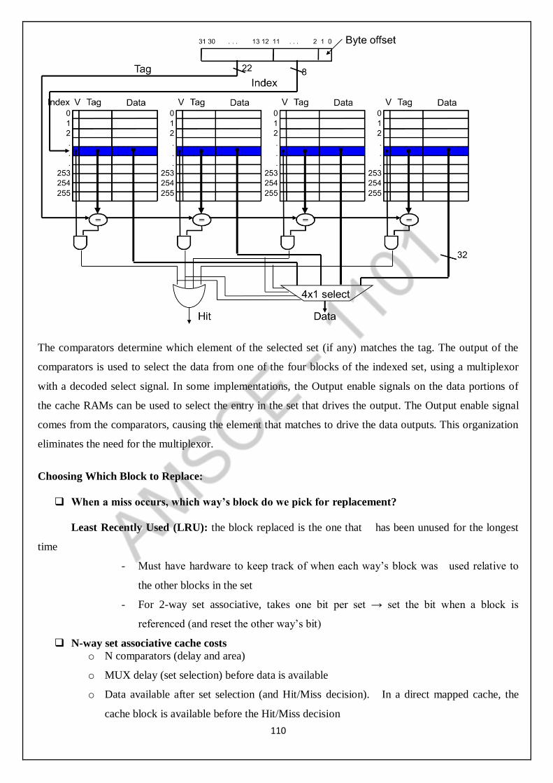
110
The comparators determine which element of the selected set (if any) matches the tag. The output of the
comparators is used to select the data from one of the four blocks of the indexed set, using a multiplexor
with a decoded select signal. In some implementations, the Output enable signals on the data portions of
the cache RAMs can be used to select the entry in the set that drives the output. The Output enable signal
comes from the comparators, causing the element that matches to drive the data outputs. This organization
eliminates the need for the multiplexor.
Choosing Which Block to Replace:
When a miss occurs, which way’s block do we pick for replacement?
Least Recently Used (LRU): the block replaced is the one that has been unused for the longest
time
- Must have hardware to keep track of when each way’s block was used relative to
the other blocks in the set
- For 2-way set associative, takes one bit per set → set the bit when a block is
referenced (and reset the other way’s bit)
N-way set associative cache costs
o N comparators (delay and area)
o MUX delay (set selection) before data is available
o Data available after set selection (and Hit/Miss decision). In a direct mapped cache, the
cache block is available before the Hit/Miss decision
111
So its not possible to just assume a hit and continue and recover later if it was a miss
Reducing the Miss Penalty Using Multilevel Caches:
Use multiple levels of caches
With advancing technology have more than enough room on the die for bigger L1 caches or for a second
level of caches – normally a unified L2 cache (i.e., it holds both instructions and data) and in some cases
even a unified L3 cache.
Problem:
CPIideal of 2, 100 cycle miss penalty (to main memory), 36% load/stores, a 2% (4%) L1I$ (D$) miss rate,
add a UL2$ that has a 25 cycle miss penalty and a 0.5% miss rate
CPIstalls = 2 + .02×25 + .36×.04×25 + .005×100 + .36×.005×100 = 3.54
(as compared to 5.44 with no L2$)
Design considerations for L1 and L2 caches are very different:
Primary cache should focus on minimizing hit time in support of a shorter clock cycle
Smaller with smaller block sizes
Secondary cache(s) should focus on reducing miss rate to reduce the penalty of long main memory
access times
Larger with larger block sizes
The miss penalty of the L1 cache is significantly reduced by the presence of an L2
cache – so it can be smaller (i.e., faster) but have a higher miss rate
For the L2 cache, hit time is less important than miss rate:
o The L2$ hit time determines L1$’s miss penalty
o L2$ local miss rate >> than the global miss rate
5. What is virtual memory and explain virtual memory with neat diagram. NOV/DEC 2015,
APR/MAY 2015, APR/MAY 2017, APR/MAY 2018
Virtual Memory:
The main memory can act as a cache for the secondary storage, usually implemented with magnetic
disks. This technique is called virtual memory.
Main memory need contain only the active portions of the many virtual machines, just as a cache
contains only the active portion of one program.
112
The virtual machines sharing the memory change dynamically while the virtual machines are
running.
Two major motivations for virtual memory:
1. to allow efficient and safe sharing of memory among multiple programs.
2. to allow a single user program to exceed the size of primary memory.
Virtual memory mechanism:
Page: A virtual memory block is called a page.
Page fault: An event that occurs when an access page is not present in main memory is called a page
fault.
Virtual address: An address that corresponds to a location in virtual space and is translated by address
mapping to a physical address when memory is accessed.
Protection: A set of mechanisms for ensuring that multiple processes sharing the processor, memory, or
I/O devices cannot interfere, intentionally or unintentionally, with one another by reading or writing each
other’s data. These mechanisms also isolate the operating system from a user process.
Address translation: The virtually addressed memory with pages mapped to main memory. This process
is called address mapping or address translation.
In virtual memory, blocks of memory (called pages) are mapped from one set of addresses (called
virtual addresses) to another set (called physical addresses).
The processor generates virtual addresses while the memory is accessed using physical addresses.
Both the virtual memory and the physical memory are broken into pages, so that a virtual page is
mapped to a physical page.
It is also possible for a virtual page to be absent from main memory and not be mapped to a
physical address; in that case, the page resides on disk.
Physical pages can be shared by having two virtual addresses point to the same physical address.
This capability is used to allow two diff erent programs to share
113
Mapping from a virtual to physical address:
A virtual address is translated to a physical address by a combination of hardware and software
So each memory request first requires an address translation from the virtual space to the physical
space
A virtual memory miss (i.e., when the page is not in physical memory) is called a page fault
The primary technique used here is to allow fully associative placement of pages in memory.
Page faults can be handled in soft ware because the overhead will be small compared to the disk
access time.
Placing a Page and Finding It Again:
Because of the incredibly high penalty for a page fault, designers reduce page fault frequency by
optimizing page placement. If we allow a virtual page to be mapped to any physical page, the operating
system can then choose to replace any page it wants when a page fault occurs.
Page table:
The table containing the virtual to physical address translations in a virtual memory system.
The table, which is stored in memory, is typically indexed by the virtual page number; each entry in the
table contains the physical page number for that virtual page if the page is currently in memory.
The page table is indexed with the virtual page number to obtain the corresponding portion of the
physical address:
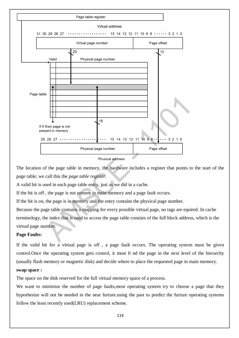
114
The location of the page table in memory, the hardware includes a register that points to the start of the
page table; we call this the page table register.
A valid bit is used in each page table entry, just as we did in a cache.
If the bit is off , the page is not present in main memory and a page fault occurs.
If the bit is on, the page is in memory and the entry contains the physical page number.
Because the page table contains a mapping for every possible virtual page, no tags are equired. In cache
terminology, the index that is used to access the page table consists of the full block address, which is the
virtual page number.
Page Faults:
If the valid bit for a virtual page is off , a page fault occurs. The operating system must be given
control.Once the operating system gets control, it must fi nd the page in the next level of the hierarchy
(usually flash memory or magnetic disk) and decide where to place the requested page in main memory.
swap space :
The space on the disk reserved for the full virtual memory space of a process.
We want to minimize the number of page faults,most operating system try to choose a page that they
hypothesize will not be needed in the near furture.using the past to predict the furture operating systems
follow the least recently used(LRU) replacement scheme.
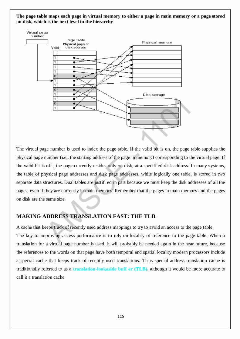
115
The page table maps each page in virtual memory to either a page in main memory or a page stored
on disk, which is the next level in the hierarchy
The virtual page number is used to index the page table. If the valid bit is on, the page table supplies the
physical page number (i.e., the starting address of the page in memory) corresponding to the virtual page. If
the valid bit is off , the page currently resides only on disk, at a specifi ed disk address. In many systems,
the table of physical page addresses and disk page addresses, while logically one table, is stored in two
separate data structures. Dual tables are justifi ed in part because we must keep the disk addresses of all the
pages, even if they are currently in main memory. Remember that the pages in main memory and the pages
on disk are the same size.
MAKING ADDRESS TRANSLATION FAST: THE TLB:
A cache that keeps track of recently used address mappings to try to avoid an access to the page table.
The key to improving access performance is to rely on locality of reference to the page table. When a
translation for a virtual page number is used, it will probably be needed again in the near future, because
the references to the words on that page have both temporal and spatial locality modern processors include
a special cache that keeps track of recently used translations. Th is special address translation cache is
traditionally referred to as a translation-lookaside buff er (TLB), although it would be more accurate to
call it a translation cache.
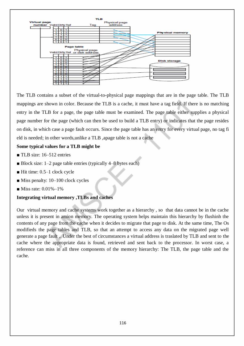
116
The TLB contains a subset of the virtual-to-physical page mappings that are in the page table. The TLB
mappings are shown in color. Because the TLB is a cache, it must have a tag field. If there is no matching
entry in the TLB for a page, the page table must be examined. The page table either supplies a physical
page number for the page (which can then be used to build a TLB entry) or indicates that the page resides
on disk, in which case a page fault occurs. Since the page table has an entry for every virtual page, no tag fi
eld is needed; in other words,unlike a TLB ,apage table is not a cache
Some typical values for a TLB might be
■ TLB size: 16–512 entries
■ Block size: 1–2 page table entries (typically 4–8 bytes each)
■ Hit time: 0.5–1 clock cycle
■ Miss penalty: 10–100 clock cycles
■ Miss rate: 0.01%–1%
Integrating virtual memory ,TLBs and caches
Our virtual memory and cache systems work together as a hierarchy , so that data cannot be in the cache
unless it is present in amion memory. The operating system helps maintain this hierarchy by flushinh the
contents of any page from the cache when it decides to migrate that page to disk. At the same time, The Os
modifieds the page tables and TLB, so that an attempt to access any data on the migrated page well
generate a page fault ,. Under the best of circumstances a virtual address is traslated by TLB and sent to the
cache where the appropriate data is found, retrieved and sent back to the processor. In worst case, a
reference can miss in all three components of the memory hierarchy: The TLB, the page table and the
cache.
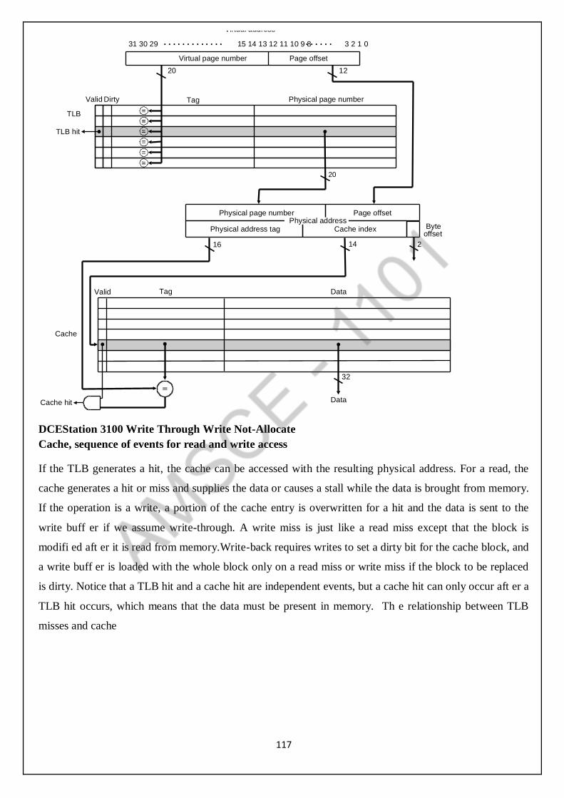
117
DCEStation 3100 Write Through Write Not-Allocate
Cache, sequence of events for read and write access
If the TLB generates a hit, the cache can be accessed with the resulting physical address. For a read, the
cache generates a hit or miss and supplies the data or causes a stall while the data is brought from memory.
If the operation is a write, a portion of the cache entry is overwritten for a hit and the data is sent to the
write buff er if we assume write-through. A write miss is just like a read miss except that the block is
modifi ed aft er it is read from memory.Write-back requires writes to set a dirty bit for the cache block, and
a write buff er is loaded with the whole block only on a read miss or write miss if the block to be replaced
is dirty. Notice that a TLB hit and a cache hit are independent events, but a cache hit can only occur aft er a
TLB hit occurs, which means that the data must be present in memory. Th e relationship between TLB
misses and cache
Valid Tag Data
Page offset
Page offset
Virtual page number
Virtual address
Physical page numberValid
1220
20
16 14
Cache index
32
Cache
DataCache hit
2
Byte offset
Dirty Tag
TLB hit
Physical page number
Physical address tag
TLB
Physical address
31 30 29 15 14 13 12 11 10 9 8 3 2 1 0
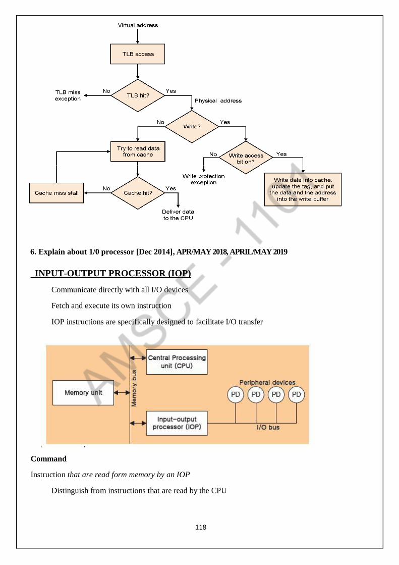
118
6. Explain about 1/0 processor [Dec 2014], APR/MAY 2018, APRIL/MAY 2019
INPUT-OUTPUT PROCESSOR (IOP)
Communicate directly with all I/O devices
Fetch and execute its own instruction
IOP instructions are specifically designed to facilitate I/O transfer
Command
Instruction that are read form memory by an IOP
Distinguish from instructions that are read by the CPU
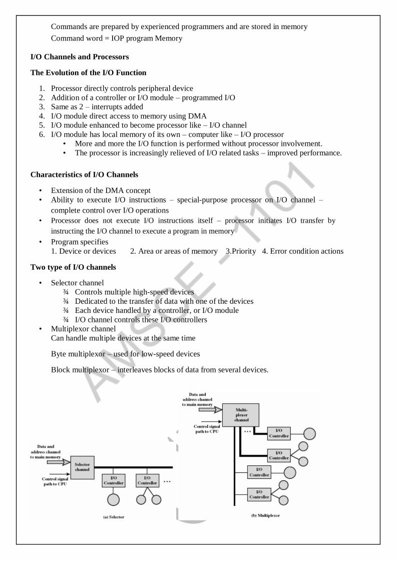
119
Commands are prepared by experienced programmers and are stored in memory
Command word = IOP program Memory
I/O Channels and Processors
The Evolution of the I/O Function
1. Processor directly controls peripheral device
2. Addition of a controller or I/O module – programmed I/O
3. Same as 2 – interrupts added
4. I/O module direct access to memory using DMA
5. I/O module enhanced to become processor like – I/O channel
6. I/O module has local memory of its own – computer like – I/O processor
• More and more the I/O function is performed without processor involvement.
• The processor is increasingly relieved of I/O related tasks – improved performance.
Characteristics of I/O Channels
• Extension of the DMA concept
• Ability to execute I/O instructions – special-purpose processor on I/O channel –
complete control over I/O operations
• Processor does not execute I/O instructions itself – processor initiates I/O transfer by
instructing the I/O channel to execute a program in memory
• Program specifies
1. Device or devices 2. Area or areas of memory 3.Priority 4. Error condition actions
Two type of I/O channels
• Selector channel
¾ Controls multiple high-speed devices
¾ Dedicated to the transfer of data with one of the devices
¾ Each device handled by a controller, or I/O module
¾ I/O channel controls these I/O controllers
• Multiplexor channel
Can handle multiple devices at the same time
Byte multiplexor – used for low-speed devices
Block multiplexor – interleaves blocks of data from several devices.
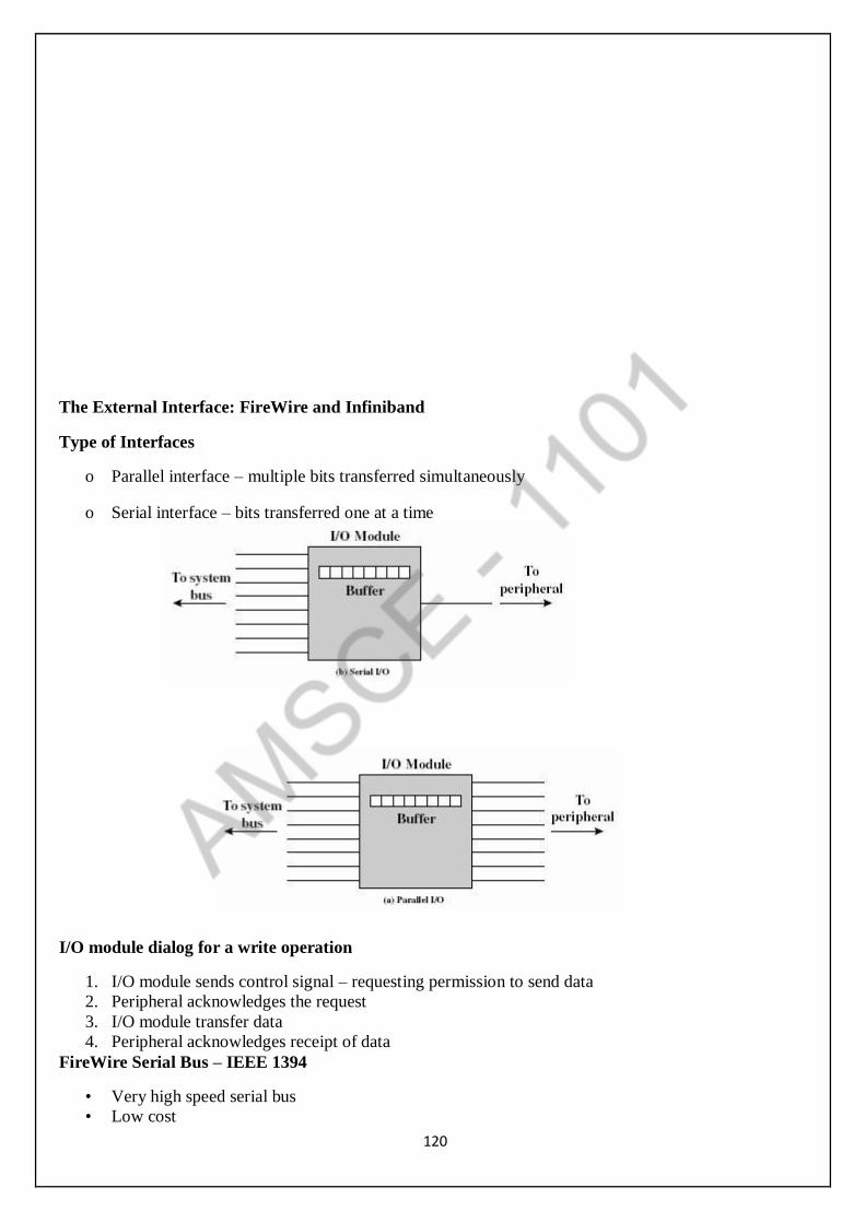
120
The External Interface: FireWire and Infiniband
Type of Interfaces
o Parallel interface – multiple bits transferred simultaneously
o Serial interface – bits transferred one at a time
I/O module dialog for a write operation
1. I/O module sends control signal – requesting permission to send data
2. Peripheral acknowledges the request
3. I/O module transfer data
4. Peripheral acknowledges receipt of data
FireWire Serial Bus – IEEE 1394
• Very high speed serial bus
• Low cost
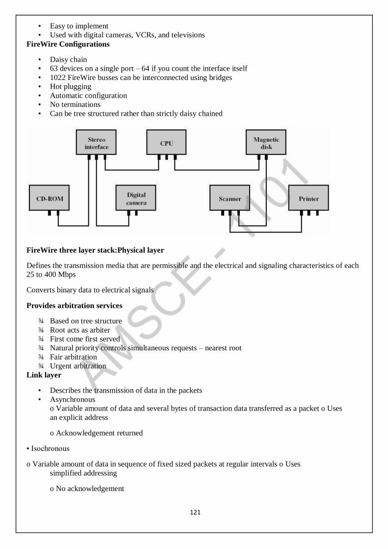
121
• Easy to implement
• Used with digital cameras, VCRs, and televisions
FireWire Configurations
• Daisy chain
• 63 devices on a single port – 64 if you count the interface itself
• 1022 FireWire busses can be interconnected using bridges
• Hot plugging
• Automatic configuration
• No terminations
• Can be tree structured rather than strictly daisy chained
FireWire three layer stack:Physical layer
Defines the transmission media that are permissible and the electrical and signaling characteristics of each
25 to 400 Mbps
Converts binary data to electrical signals
Provides arbitration services
¾ Based on tree structure
¾ Root acts as arbiter
¾ First come first served
¾ Natural priority controls simultaneous requests – nearest root
¾ Fair arbitration
¾ Urgent arbitration
Link layer
• Describes the transmission of data in the packets
• Asynchronous
o Variable amount of data and several bytes of transaction data transferred as a packet o Uses
an explicit address
o Acknowledgement returned
• Isochronous
o Variable amount of data in sequence of fixed sized packets at regular intervals o Uses
simplified addressing
o No acknowledgement
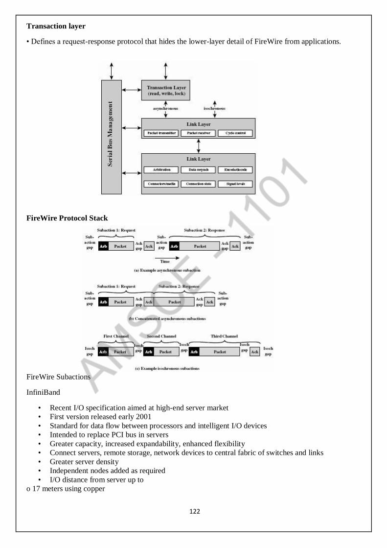
122
Transaction layer
• Defines a request-response protocol that hides the lower-layer detail of FireWire from applications.
FireWire Protocol Stack
FireWire Subactions
InfiniBand
• Recent I/O specification aimed at high-end server market
• First version released early 2001
• Standard for data flow between processors and intelligent I/O devices
• Intended to replace PCI bus in servers
• Greater capacity, increased expandability, enhanced flexibility
• Connect servers, remote storage, network devices to central fabric of switches and links
• Greater server density
• Independent nodes added as required
• I/O distance from server up to
o 17 meters using copper
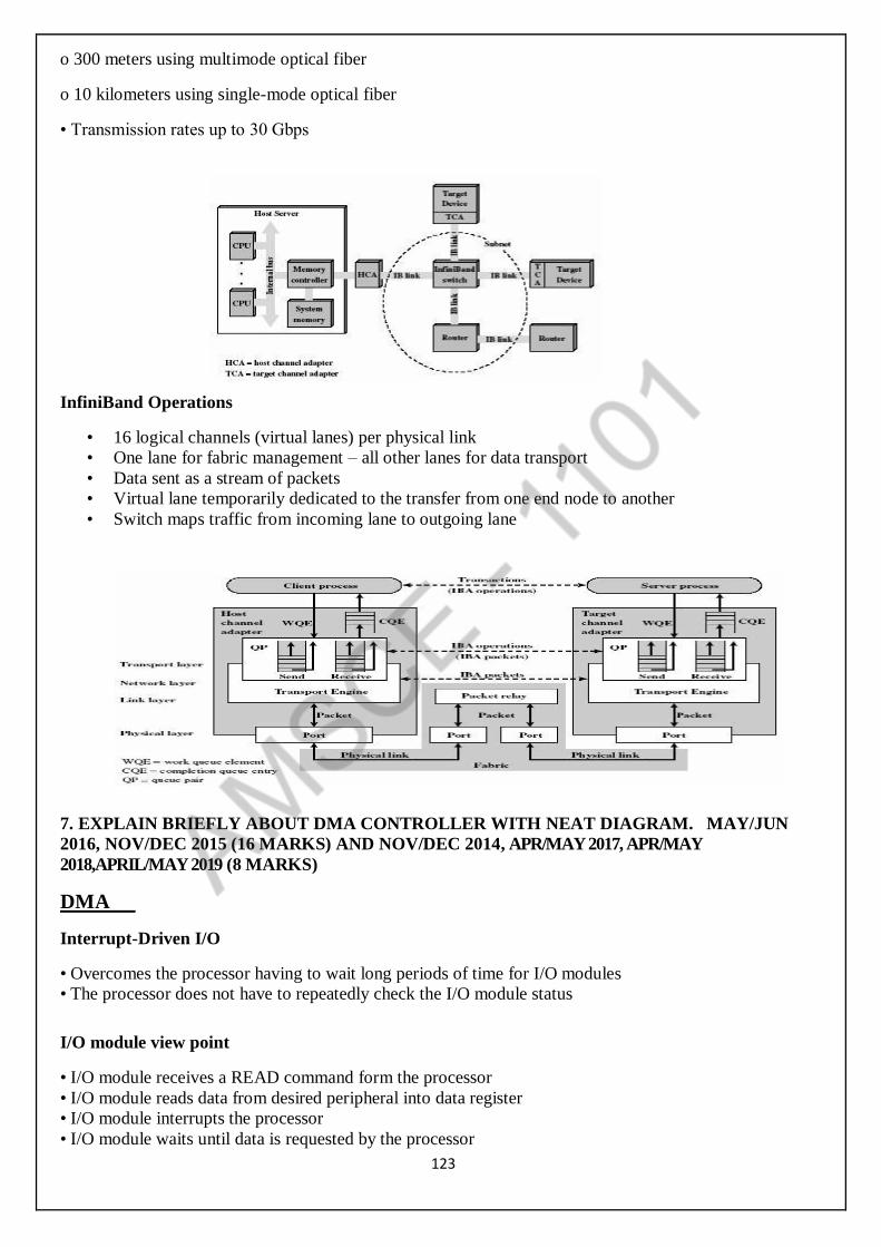
123
o 300 meters using multimode optical fiber
o 10 kilometers using single-mode optical fiber
• Transmission rates up to 30 Gbps
InfiniBand Operations
• 16 logical channels (virtual lanes) per physical link
• One lane for fabric management – all other lanes for data transport
• Data sent as a stream of packets
• Virtual lane temporarily dedicated to the transfer from one end node to another
• Switch maps traffic from incoming lane to outgoing lane
7. EXPLAIN BRIEFLY ABOUT DMA CONTROLLER WITH NEAT DIAGRAM. MAY/JUN
2016, NOV/DEC 2015 (16 MARKS) AND NOV/DEC 2014, APR/MAY 2017, APR/MAY
2018,APRIL/MAY 2019 (8 MARKS)
DMA
Interrupt-Driven I/O
• Overcomes the processor having to wait long periods of time for I/O modules
• The processor does not have to repeatedly check the I/O module status
I/O module view point
• I/O module receives a READ command form the processor
• I/O module reads data from desired peripheral into data register
• I/O module interrupts the processor
• I/O module waits until data is requested by the processor
124
• I/O module places data on the data bus when requested
Processor view point
• The processor issues a READ command
• The processor performs some other useful work
• The processor checks for interrupts at the end of the instruction cycle
• The processor saves the current context when interrupted by the I/O module
• The processor read the data from the I/O module and stores it in memory
• The processor the restores the saved context and resumes execution
Design Issues
a. How does the processor determine which device issued the interrupt
b. How are multiple interrupts dealt with
c. Device identification
d. Multiple interrupt lines – each line may have multiple I/O modules
e. Software poll – poll each I/O module
f. Separate command line – TESTI/O
g. Processor read status register of I/O module Time consuming
h. Daisy chain
i. Hardware poll
j. Common interrupt request line Processor
sends interrupt acknowledge
k. Requesting I/O module places a word of data on the data lines – ―vector‖ that uniquely
identifies the I/O module – vectored interrupt
• Bus arbitration
¾ I/O module first gains control of the bus
¾ I/O module sends interrupt request
¾ The processor acknowledges the interrupt request
¾ I/O module places its vector of the data lines
Multiple interrupts
• The techniques above not only identify the requesting I/O module but provide methods of assigning
priorities
• Multiple lines – processor picks line with highest priority
• Software polling – polling order determines priority
• Daisy chain – daisy chain order of the modules determines priority
• Bus arbitration – arbitration scheme determines priority
Intel 82C59A Interrupt Controller
Intel 80386 provides
• Single Interrupt Request line – INTR
• Single Interrupt Acknowledge line – INTA
• Connects to an external interrupt arbiter, 82C59A, to handle multiple devices and priority structures
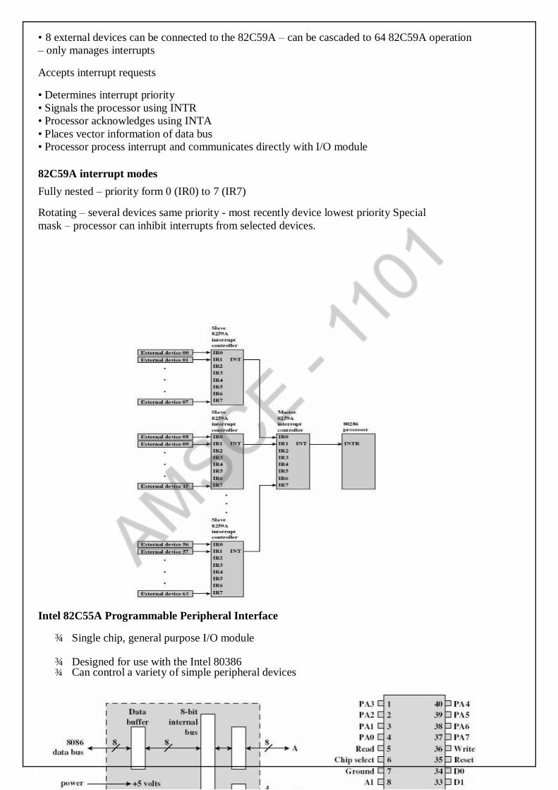
125
• 8 external devices can be connected to the 82C59A – can be cascaded to 64 82C59A operation
– only manages interrupts
Accepts interrupt requests
• Determines interrupt priority
• Signals the processor using INTR
• Processor acknowledges using INTA
• Places vector information of data bus
• Processor process interrupt and communicates directly with I/O module
82C59A interrupt modes
Fully nested – priority form 0 (IR0) to 7 (IR7)
Rotating – several devices same priority - most recently device lowest priority Special
mask – processor can inhibit interrupts from selected devices.
Intel 82C55A Programmable Peripheral Interface
¾ Single chip, general purpose I/O module
¾ Designed for use with the Intel 80386 ¾ Can control a variety of simple peripheral devices
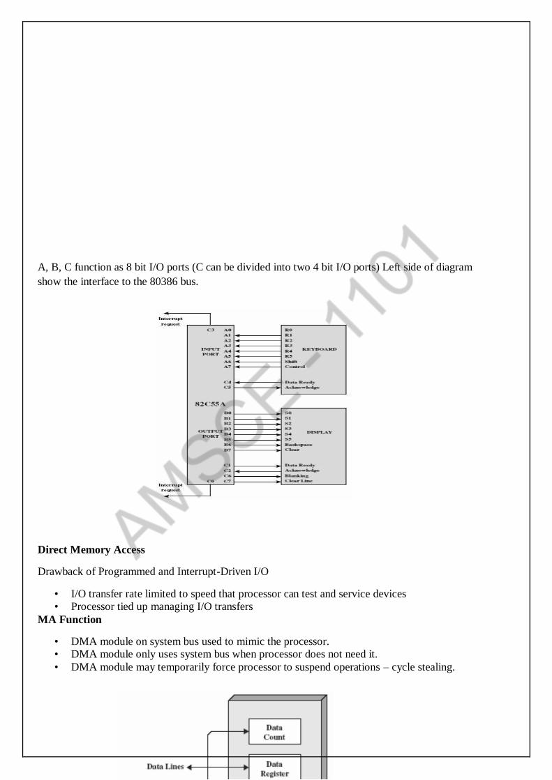
126
A, B, C function as 8 bit I/O ports (C can be divided into two 4 bit I/O ports) Left side of diagram
show the interface to the 80386 bus.
Direct Memory Access
Drawback of Programmed and Interrupt-Driven I/O
• I/O transfer rate limited to speed that processor can test and service devices
• Processor tied up managing I/O transfers
MA Function
• DMA module on system bus used to mimic the processor.
• DMA module only uses system bus when processor does not need it.
• DMA module may temporarily force processor to suspend operations – cycle stealing.
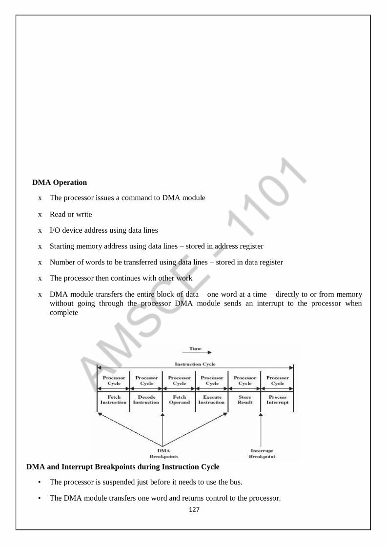
127
DMA Operation
x The processor issues a command to DMA module
x Read or write
x I/O device address using data lines
x Starting memory address using data lines – stored in address register
x Number of words to be transferred using data lines – stored in data register
x The processor then continues with other work
x DMA module transfers the entire block of data – one word at a time – directly to or from memory
without going through the processor DMA module sends an interrupt to the processor when
complete
DMA and Interrupt Breakpoints during Instruction Cycle
• The processor is suspended just before it needs to use the bus.
• The DMA module transfers one word and returns control to the processor.
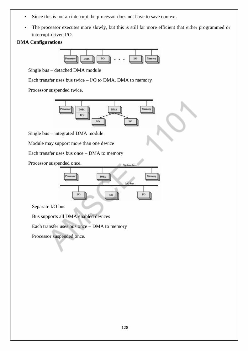
128
• Since this is not an interrupt the processor does not have to save context.
• The processor executes more slowly, but this is still far more efficient that either programmed or
interrupt-driven I/O.
DMA Configurations
Single bus – detached DMA module
Each transfer uses bus twice – I/O to DMA, DMA to memory
Processor suspended twice.
Single bus – integrated DMA module
Module may support more than one device
Each transfer uses bus once – DMA to memory
Processor suspended once.
Separate I/O bus
Bus supports all DMA enabled devices
Each transfer uses bus once – DMA to memory
Processor suspended once.


![RISC, CISC, and Assemblers - Cornell University · RISC, CISC, and Assemblers ... • Complexity: CISC, RISC Assemblers ... –e.g. Mem[segment + reg + reg*scale + offset] 14 RISC](https://static.fdocuments.us/doc/165x107/5c1068af09d3f254228c84fd/risc-cisc-and-assemblers-cornell-risc-cisc-and-assemblers-complexity.jpg)