Cryogenic Dark Matter Search Detector Fabrication Process ... · PDF filelm characterization...
32
Cryogenic Dark Matter Search Detector Fabrication Process and Recent Improvements A. Jastram a,* , H. R. Harris a , R. Mahapatra a , J. Phillips a , M. Platt a , K. Prasad a , J. Sander a,b , S. Upadhyayula a a Department of Physics & Astronomy, Texas A&M University, College Station, TX 77843, USA b Department of Physics, University of South Dakota, Vermillion, SD 57069, USA Abstract A dedicated facility has been commissioned for Cryogenic Dark Matter Search (CDMS) detector fabrication at Texas A&M University (TAMU). The fabrication process has been carefully tuned using this facility and its equipment. Production of successfully tested detectors has been demonstrated. Significant improvements in detector performance have been made using new fabrication methods/equipment and tuning of process parameters. 1. Introduction The quest for an understanding of Dark Matter is at the forefront of particle physics today. One proposed constituent of Dark Matter is a particle called the WIMP (Weakly Interacting Massive Particle). Many experiments around the world are attempting to directly detect this particle in order to further under- stand the nature of Dark Matter. CDMS (Cryogenic Dark Matter Search) is one of these experiments, utilizing ground based detectors sensitive to nuclear recoils caused by direct collisions with these particles. These detectors, com- posed of germanium or silicon, are instrumented to detect deposition of both ionization and phonon energy upon interaction with an incident particle. Using these two signals and clever detector design[1], electron recoils (characteristic * Corresponding author Email address: [email protected] (A. Jastram) Preprint submitted to Nuclear Instruments and Methods in Physics ResearchSeptember 29, 2014 arXiv:1408.0295v3 [physics.ins-det] 26 Sep 2014
Transcript of Cryogenic Dark Matter Search Detector Fabrication Process ... · PDF filelm characterization...

Cryogenic Dark Matter Search Detector FabricationProcess and Recent Improvements
A. Jastrama,∗, H. R. Harrisa, R. Mahapatraa, J. Phillipsa, M. Platta, K.Prasada, J. Sandera,b, S. Upadhyayulaa
aDepartment of Physics & Astronomy, Texas A&M University, College Station, TX 77843,USA
bDepartment of Physics, University of South Dakota, Vermillion, SD 57069, USA
Abstract
A dedicated facility has been commissioned for Cryogenic Dark Matter
Search (CDMS) detector fabrication at Texas A&M University (TAMU). The
fabrication process has been carefully tuned using this facility and its equipment.
Production of successfully tested detectors has been demonstrated. Significant
improvements in detector performance have been made using new fabrication
methods/equipment and tuning of process parameters.
1. Introduction
The quest for an understanding of Dark Matter is at the forefront of particle
physics today. One proposed constituent of Dark Matter is a particle called the
WIMP (Weakly Interacting Massive Particle). Many experiments around the
world are attempting to directly detect this particle in order to further under-
stand the nature of Dark Matter. CDMS (Cryogenic Dark Matter Search) is
one of these experiments, utilizing ground based detectors sensitive to nuclear
recoils caused by direct collisions with these particles. These detectors, com-
posed of germanium or silicon, are instrumented to detect deposition of both
ionization and phonon energy upon interaction with an incident particle. Using
these two signals and clever detector design[1], electron recoils (characteristic
∗Corresponding authorEmail address: [email protected] (A. Jastram)
Preprint submitted to Nuclear Instruments and Methods in Physics ResearchSeptember 29, 2014
arX
iv:1
408.
0295
v3 [
phys
ics.
ins-
det]
26
Sep
2014

of the dominant background signals) can be discriminated from nuclear recoils
(characteristic of a WIMP-like interaction). To continue probing new parameter
space, greater sensitivity is needed for each generation of experiment, requiring
significant improvements in the detector technology used to reject electron re-
coils and fabrication throughput. While many of these improvements are being
made in readout electronics and analysis procedures, the underlying quality of
the initial data, and therefore the quality of the detectors, is a fundamental
limit[2]. Detector uniformity and consistency are also important, particularly
when scaling up in size and quantity of detectors. Great strides in both of these
areas have been made at the TAMU facilities. Serving as a second fabrication
facility and now the dominant polishing facility, the increased throughput will
allow the next generation experiment to produce the required detector payload
on a competitive timescale.
2. Fabrication
CDMS detectors are produced using techniques and equipment similar to
those in typical semiconductor fabrication processes. The process begins with
high quality semiconductor substrates (germanium or silicon) and uses pho-
tolithography to etch deposited films into circuit structures (see Figure 1). One
significant difference, however, is that the substrates used for CDMS detectors
are much thicker, ranging from 10mm in original designs to 33.3mm in current
production. For this reason, semiconductor equipment and processing typically
used for ∼1mm thick substrates have been modified and tuned for these larger
detector geometries.
2.1. Substrate Materials
Detectors are fabricated on high purity germanium and silicon substrates.
For detector quality germanium substrates, “high purity” equates to impurity
levels typically on the order of 1010cm−3 . These are grown using the Czochralski
Process. Substrates used for this experiment typically have dislocation densi-
ties of 1000-7000cm−2. For silicon detectors, quality is specified/determined
2

Align/
Shape
Polish
Film Deposition
Photo-lithography
Mount/
Package
Etch
Metrology
Heavy Etch
Clean
Inspection/
Surgery
Figure 1: Process flow chart from raw substrate to completion (see Section 2).
by room temperature resistivity. While >8 kΩ-cm is the specification for ac-
ceptable material, typical detector quality substrates have a resistivity of >20
kΩ-cm and are grown using the Float Zone Process. All detectors currently
operating in the SuperCDMS Soudan experiment are 76mm diameter x 25mm
thick germanium substrates. The next generation will utilize both silicon and
germanium detectors, 100mm diameter by 33.3mm thick[3]. The majority of this
R&D, including establishment and tuning of the fabrication process (specifically
film characterization and photolithography steps), is performed using low resis-
tivity commercial “Prime Grade” silicon wafers (75mm and 100mm diameter
with SEMI Standard1 thickness and flats). Being much lower in cost, easier
to obtain, and easier to clean/prepare than thick substrates, they are a natu-
ral choice for practice and R&D. Once established, fabrication procedures are
1Standards/specifications available from www.semi.org
3
then tested/confirmed on thick substrates. Low purity/price thick substrates
are used for this before fabricating detector quality substrates.
2.2. Alignment and Shaping
To improve uniformity and charge collection performance among the de-
tectors, the substrates are shaped and aligned to a specific crystal axis and
orientation. Upon delivery from the vendor, the cylindrical substrates are guar-
anteed to be aligned within ±2 of the target crystal axis, typically [100]. For
improved ionization drift/collection, they are subsequently re-shaped with the
alignment refined to ±0.1 . For this reason, the substrates, as purchased, are
slightly over-sized in all dimensions to account for material loss in re-shaping.
Re-shaping consists of aligning and grinding the substrates’ faces, followed by
grinding the cylindrical sidewall. A custom fixture has been made to allow the
surface plane of the substrate to be manipulated with micrometers to precisely
dial in the crystallographic axis to the coordinates of the x-ray diffractome-
ter (XRD) used in this alignment process. For more information on the XRD
process, see [4]. In this setup, a modified Rigaku DMAX-1BX is used with
the x-ray source operated at 30kV and 20mA. First, the face of the substrate
is positioned/aligned to the point of initial interference with the x-ray beam
(which is set to 2θ=0 ) with the face parallel to the beam and perpendicular
to the goniometer’s θ plane. The goniometer is then set to the Bragg angle of
the target crystal axis and a local 2θ sweep is performed (the width of which
is dictated by the alignment tolerance from the vendor). This produces a peak
near the Bragg angle which will shift according to aforementioned micrometer
adjustments. These adjustments and measurements are made iteratively (gross
adjustments at first, followed by fine tuning) until the peak is within the re-
quired tolerance of the appropriate Bragg angle. The crystal is then locked into
that orientation in the alignment fixture, which is designed such that it can
be unmounted from the XRD system and attached to a grinding fixture. This
assembly is then placed on a Lapmaster 24C lapping machine (equipped with a
220 grit diamond magnetic plate) such that the substrate feeds into the grind-
4

ing surface along the crystal axis. After grinding, this surface is measured again
using XRD to confirm successful alignment. The second face is then ground
parallel to the first using this same fixture. Parallelism of the faces is confirmed
using a granite indicator stand. The cylindrical sidewall must then be shaped
parallel to the crystal axis. To reduce the chance of chipping during this pro-
cess, circular plates of glass (1/8” thick with a diameter 0.25” larger than the
final substrate diameter) are bonded to each face with a wax bonder using 69 C
quartz wax. The sidewall shape is then defined using a diamond coring fixture.
The coring diameter is that of the final substrate specification. The glass plates
and quartz wax are then removed. To provide room for interface boards in the
detector housings (see Section 2.8) and ensure all crystals are fabricated in a
uniform rotational orientation, flats are ground on the sidewall of the substrate.
These are located normal to a specific crystallographic direction ([011] in the
case of [100] crystals). To perform this alignment, the crystal is loaded into a
custom XRD mount with the previously aligned crystal axis normal to the 2θ
plane and the x-ray beam incident upon the sidewall (with the sidewall now po-
sitioned to just slightly interfere with the beam while 2θ=0 ). The goniometer
is then set to the Bragg angle of the desired flat orientation, and the crystal is
rotated about its axis (in the 2θ plane) using a precision rotary table indexer
until the diffracted intensity is maximized (locating the orientation to ±1 ).
Using a custom jig, the two diametrically opposed flats are ground using the
Lapmaster 24C. The crystal is then lapped (on the same machine) to its desired
thickness.
2.3. Heavy Etch
In order to remove substrate surfaces that may have been contaminated by
previous processing and/or exposure to radon-containing atmosphere, the sub-
strates are then chemically etched2. This process removes the outer layer (up to
2This etch recipe is based on a process described in [5] modified by Paul Brink and Larry
Novak.
5

∼250µm) of material, which is assumed to be contaminated/compromised. Sil-
icon substrate etching has not been used by CDMS in the past, but is currently
under development for future detectors. Germanium etching is performed in
the following solution:
1. 3200mL 69% HNO3
2. 640mL 50% HF
3. 150mL CH3CO2H (glacial)
The substrate is dipped in the etchant using a modified PTFE wafer cassette
(used in all subsequent acid processing) and agitated lightly by hand, followed
by a dip in de-ionized (DI) water. This is repeated 10 times. It is then placed
in a Verteq 1600-55M spin rinse/dryer for a standard rinse/dry process (to be
referred to as SRD). The SRD process consists of the following steps:
1. 35 seconds @600rpm with N2 purge and DI spray
2. 230 seconds @1600rpm with heated N2 purge
3. 90 seconds @1600rpm with N2 purge
Following this step, substrates are stored in nitrogen purged cabinets when not
being actively processed, reducing subsequent exposure to ambient radon.
2.4. Lapping/Polishing
Photolithographic processing of micron scale features requires a smooth,
featureless substrate surface. For this reason, the coarsely lapped, heavy-etched
detector faces must be polished. This is accomplished via four sequential steps:
1. Fine-grit manual lapping
2. Surface shaping polish
3. Scratch-removing polish
4. Final surface treatment polish
Substrates are hand-lapped on a slotted glass lapping plate using 9µm alumina
polishing powder mixed with DI water to form a paste consistency. This is to
remove large features from the surface. The surfaces must then be polished to a
6

specified flatness with a mirror finish, free of visible features (such as scratches or
pits) to facilitate uniform film depositions and prevent circuit defects (see Figure
6) in subsequent processing. Polishing is performed on a dual spindle polishing
machine. Control of surface curvature (concavity vs. convexity) is maintained
with polisher settings and various sizes of polishing pads surfaced with polyester
material in a 1:1 mixture of colloidal alumina polishing compound:DI water.
This process is carefully controlled such that the final surface has <2µm of total
height deviation across the substrate if convex, <1µm if concave (curvature is
measured with a desktop laser interferometer). This is to ensure uniform contact
with the photo mask (which can conform slightly to convexity but not concavity)
during the photolithography process. Small surface scratches resulting from this
step are then removed on the same machine using “regular nap” polyurethane
pads and a fresh mixture of the same polishing slurry. Final surface polishing
is performed with “high nap” polyurethane pads in a colloidal silica polishing
compound. Final surface inspection is performed using a stereo zoom binocular
microscope, manually confirming a defect free mirror finish.
2.5. Cleaning
Before the polished substrates can be processed into detectors, they must be
cleaned carefully. This removes surface contaminants as well as any particulates
that may cause defects in subsequent processing (see Section 2.8). For this
reason, the cleaning is performed in a class 100 clean room. Germanium and
silicon substrates require different cleaning processes, germanium’s being much
more time and labor intensive (another benefit of using silicon wafers for R&D).
2.5.1. Germanium
Initial germanium cleaning involves a 5 minute soak in acetone followed by
a 5 minute soak in isopropyl alcohol (NOTE: all chemicals used in cleaning
and subsequent processing are semiconductor grade). Following a thorough
rinse with DI water, the surfaces are manually inspected using a microscope
equipped with an LED ring light (especially effective for identifying particles on
7
the surface as it exposes diffuse features). If particulate count is unacceptable
(≥10cm−2), the previous chemical process is repeated, and the crystal is dried
using a filtered nitrogen gun. If particulate count is still unacceptable, the
substrate is rinsed with methanol and manually wiped with a PVA cleaning
brush. If the surface condition is still unacceptable, the methanol and brush
wipe is repeated as necessary. Otherwise, the substrate proceeds to the oxide
removal step. For this, a mixture of 3:1 DI water:50%HF is prepared in which
the substrate is submersed for 5 minutes followed by a 3 minute soak in DI water.
This is repeated three times and followed by surface inspection. If particulate
count has become unacceptable, a methanol rinse and brush wipe are repeated
as necessary. Upon completion, the substrate is placed in the oven at 120 C for
10 minutes to bake out remaining moisture.
2.5.2. Silicon
Silicon substrates also receive chemical cleaning, but have not shown the
need for manual particulate removal. In the cleaning process, the substrates
are initially doused with methanol then isopropyl alcohol, followed by SRD. To
remove metals and organic contaminants, a Piranha clean process is used. This
consists of a 20 minute dunk in the following solution (heated to 55C):
1. 600mL 30% H2O2
2. 700mL 98% H2SO4
3. 1050mL 0.250N H2SO4
Substrates are then soaked in 55C DI for 1 minute, manually agitated once
every 15 seconds. To remove the native oxide from the substrates’ surfaces,
they are then placed in the following solution for 20 seconds:
1. 2700mL DI
2. 50mL 50% HF
The substrates are then dipped again in 55C DI for 1 minute, manually agitated
once every 15 seconds. To remove ionic and heavy metal atomic contaminants
8

from the substrates’ surfaces, the substrates are submersed in the following
solution, heated to 70C, for 15 minutes:
1. 1750mL DI
2. 325mL 30% H2O2
3. 300mL 37% HCl
This is followed by SRD and a 5 minute dehydrate in the oven at 120C. The
cleaning process seals the substrate with a thin oxide layer which is removed in
the sputtering system prior to film deposition (see Section 2.6).
2.6. Thin Film Deposition/Tuning
The films that form the final circuit and sensors of the detector are deposited
using a customized plasma sputtering deposition system. Precise and repeat-
able process control is vital in the deposition of these films as they dictate the
quality of the final circuit features (see Sections 3.1, 3.2, and 3.3). The depo-
sition system used in this process is a Perkin Elmer 4400 Delta with PLC/PC
interface automated by Semiconductor Engineering Group, Inc. (SEGI), which
has been modified for this fabrication process. It can simultaneously sputter 8
substrates, 100mm in diameter (or 6, 150mm diameter) and is composed of two
main vacuum chambers: the load lock and the process chamber, separated by a
gate valve. The load lock is the location in which substrates are initially loaded,
which is then pumped to 4.0x10⁻⁶ Torr using a turbo-molecular pump (added
for this process). This allows the process chamber to stay isolated from atmo-
spheric contaminants at all times (specifically when the substrate is transferred
through the gate valve into this chamber). To further reduce contaminants, a
pre-coat of Aluminum is sputtered in the process chamber as a getter. This pro-
cess removes traces of O2 and H2O (see Figure 2) as well as other contaminants
which can alter film characteristics, further improving process stability. The
substrates are then transferred into the process chamber, which is subsequently
pumped back to a base pressure of 9.0x10⁻⁷ Torr. The process chamber is cylin-
drical (∼1m in diameter) and can simultaneously accommodate three different
9

targets of sputtering materials. The chamber is equipped with aluminum, tung-
sten, and silicon targets, all of which are 99.999% pure. After substrates are
loaded in the load lock, the rest of the deposition process is entirely automated,
including everything from rotation and height settings of the table on which the
substrates sit to setting/maintaining the chamber and plasma conditions. Table
height settings are customized for each substrate thicknesses to maintain a con-
stant target-substrate distance. Other settings of particular note are the voltage
and power supplied to the target (DC or RF), DC bias applied to substrates
during deposition, flow of Argon into the chamber, and optional RF pre-etch.
The process chamber is equipped with an RGA (Residual Gas Analyzer)
which measures the contents of the gas in the process chamber. The RGA can
be used in two modes: plotting the entire spectrum at once, showing peaks at
various masses corresponding to contaminants in the chamber (see Figure 2), or
plotting the levels of a chosen contaminant over time. A high capacitance valve
is implemented to allow the RGA to operate at high vacuum levels as well as
in-process levels (∼10mTorr). This allows in-situ analysis of any possible gas
contaminants during the deposition process.
All of the above devices/processes allow the minimization of contaminants
and maximization of control and repeatability in the deposition process. Us-
ing this system, three thin film layers (designated as the trilayer) are sputtered
sequentially on both faces of each substrate: 40nm amorphous silicon (a-Si),
300nm aluminum, and 30nm tungsten. The a-Si layer underlies all final metal
circuit structures and is used to protect the substrate surface from aluminum and
tungsten etchant chemicals, as well as improving the ionization collection bound-
ary. The aluminum layer forms the phonon collection structures (see Figure 3
and Section 3.1) as well as the circuit lines/electrodes connecting the sensors on
the detector. The tungsten layer serves as a cap layer, preventing the aluminum
surface from oxidizing (see Section 3.3) and preventing back-sputtering of the
aluminum during the subsequent deposition. Before each deposition begins, the
target to be used is pre-sputtered for 25 seconds to clean its surface with its
shutter closed (to prevent sputtered material from depositing on substrates).
10
Before all depositions, an aluminum shadow mask is manually placed on the
substrate face which covers the outer ∼1mm of the exposed surface, preventing
deposition on this region (see Section 3.5) and the substrate’s sidewall surface.
The steps and parameters used for the trilayer deposition are the following:
1. 10 minute RF etch, 350 W RF, 50 sccm Ar, 10 mTorr
2. 16 minute a-Si deposition, 500 W RF, 50 sccm Ar, 8 mTorr
3. 7m18s aluminum deposition, 2.5 kW DC, 40 sccm Ar, 10 mTorr
4. 36 second tungsten deposition, 2.5 kW DC, 40 sccm Ar, 8 mTorr
The films are then patterned photolithographically and chemically etched,
forming the majority of the detector circuit (described in Section 2.7). After
chemical etching, a 40nm layer of tungsten is sputtered on each face of the
substrate. This layer forms the transition edge sensors (TES’s) of the detector
(see Sections 3.2 & 3.3). The steps/parameters used for this deposition are as
follows:
1. 10 minute RF etch, 350 W RF, 50 sccm Ar, 10 mTorr
2. 51 second tungsten deposition, 2.5 kW DC, 40 sccm Ar, 8 mTorr, 100V
DC bias delivered to substrate
2.7. Photolithography
A three step photolithographic process is used to define the circuit features
on the substrates. The original process from which this was adapted is described
in [6] and [7]. The first step defines the aluminum structures (circuit lines and
phonon collecting fins [see Section 3.1]). The second step defines the tungsten
TES features (see Section 3.2), and the third defines the a-Si structure and
substrate trenching regions (see Section 3.4). The aluminum and tungsten are
etched with chemicals, while the a-Si is plasma etched via an RIE (Reactive
Ion Etch) process. In all three steps, an etch resistive mask of photoresist is
used to protect the features while the exposed films are etched. The photoresist
mask pattern is formed via UV transfer/exposure using a master template mask.
Chemical processing of the substrates is performed in a class 100 UV-free clean
room.
11

0 10 20 30 40 50 60 70 80 90 10010−10
10−9
10−8
10−7
10−6Pre Al−bury RGA Scan Jan 13, 2011 08:53:16 AM
Molecular Mass (amu)
Par
tial P
ress
ure
(Tor
r)
0 10 20 30 40 50 60 70 80 90 10010−10
10−9
10−8
10−7
10−6Post Al−bury RGA Scan Jan 13, 2011 10:05:09 AM
Molecular Mass (amu)
Par
tial P
ress
ure
(Tor
r)Water Vapor
Neon
Argon
Oxygen
NitrogenHydrogen
Helium
Student Version of MATLAB
Figure 2: Example RGA spectra of partial pressures in the SEGI process chamber at various
atomic masses before (top) and after (bottom) aluminum getter deposition (see Section 2.6),
demonstrating the efficacy of this process in reducing oxygen and water vapor levels.
2.7.1. Trilayer Patterning
After the trilayer deposition (see Section 2.6), a Solitec 5110-SJ spin coater
is used to spin coat Shipley Microposit S1811 photoresist on both faces of the
substrate. To create and maintain a vacuum seal between the substrate and
spin coater’s chuck, 0.032” thick elastomer skirts are stretched around the sub-
strate sidewall. These are removed and discarded after the spin coat process
(see Section 3.5 for more information on the photoresist layer/process). The
substrate is then placed in the oven (in a PTFE cassette, covered with alu-
minum foil to protect the fresh photoresist from particulates) at 120 C to soft
bake the photoresist (see Table 1 for bake times). After baking, the crystal is
12

Figure 3: Image of a single phonon sensor and magnified inset of TES line and “waterfall”
region (arrow indicates waterfall boundary, see Figure 9 for closeup and Section 3.3 for descrip-
tion). Each color corresponds to the exposed film on the final structure: Blue=Aluminum
(mask #1, trilayer mask), Pink=Tungsten (mask #2, TES mask), Green=a-Si (mask #3,
“trench” mask) (see Section 2.7). The central vertical line is the ∼2µm wide TES, and the
large aluminum “fins” are the phonon absorbing structures (see Section 3.1). Note: a-Si
underlies all metal features.
allowed to cool to room temperature. The cooling process is accelerated with a
gentle stream of filtered nitrogen gas on each face. The substrate is then ready
for the photolithographic mask transfer/exposure process. An OAI 206-094735
contact aligner with a 350W Hg g-line UV lamp is used to expose each face for
5.3s at 8.15mW/cm2 using mask #1, the trilayer mask (see Figure 3). Special
care must be taken not to scratch the backside photoresist layer when placing
the substrate on the stage (and when flipping the substrate for exposure of the
second face). The UV intensity is confirmed before each exposure using an OAI
0308 UV meter tuned to 436nm (g-line). The pattern is then developed using
Shipley Microposit MF-319 developer, mildly agitated by hand, until comple-
tion. This is judged by eye, typically taking 70-90 seconds. The substrate is
gently rinsed in DI water after development, then proceeds to SRD. The pho-
toresist is then inspected to confirm successful development (robust replication
of mask structure). The substrates are then returned to the oven at 120 C to
hard bake the photoresist (see Table 1 for bake times). They are then cooled to
room temperature with the assistance of gentle nitrogen gas flow. The tungsten
layer is etched for 6m30s using 30% H2O2 with 2 gentle manual agitations at 1
13

Aluminum “fins” TES
“Trench”
Q Electrode
Polish/Clean Substrate Trilayer Deposition Spin Coat Photoresist
Expose/Develop
Mask #1Etch Tungsten
& Aluminum Strip Photoresist
Tungsten TES
Deposition
Etch Tungsten
Etch a-Si
& Substrate
Spin Coat Photoresist Expose/Develop
Mask #2
Strip Photoresist Spin Coat Photoresist
Expose/Develop
Mask #2Strip Photoresist
Figure 4: Detector patterning process (not to scale). Individual film layers are shown through-
out the deposition/photolithography process (see Section 2.7). Gray=Substrate, Green=a-Si,
Blue=Aluminum, Pink=Tungsten, and Red-brown=Photoresist.
minute intervals, followed by SRD. The aluminum layer is etched using Cyantek
Al-11. This typically consists of 5-6 iterations of the following: 45s Al-11 dunk
14

with constant gentle agitation, followed by a 15s DI rinse. The aluminum etch
leaves a slight overhang of the tungsten cap layer, due to the isotropic nature
of the reaction (see Figure 5). Intermittent DI rinses are used to control the
temperature of the exothermic etch reaction[8], improving etch uniformity and
reducing the undercut/overhang issue. When all exposed aluminum appears to
have vanished, the substrate receives an additional 15s of Al-11 etch to ensure
no aluminum remains, then proceeds to SRD. To remove the overhang feature,
another tungsten etch is performed (see Section 3.3). This consists of a 10
minute submersion in 30% H2O2, with 2 gentle agitations every 2 minutes, fol-
lowed by SRD. At this point, the circuit pattern is carefully inspected to confirm
successful etching and preserved photoresist integrity. The photoresist layer is
removed using a 20 minute dip in Shipley PRX-127 at 45 C, with 2 gentle ag-
itations every 5 minutes, followed by SRD. As a final cleaning precaution, the
substrate is submerged in Baker PRS-1000 for 10 minutes at 45 C, followed
by SRD. Etched features are then inspected (and again after each subsequent
photolithography/etch cycle), monitoring for defects and critical circuit feature
dimensions. The substrate is then placed in the SEGI under vacuum overnight
to boil off any moisture before the following tungsten (TES layer) deposition.
2.7.2. TES Patterning
The second deposition, that which forms the TES tungsten layer, is then
performed (see Section 2.6). After this deposition, the substrate receives the
same spin coat, soft bake, alignment, exposure, develop and hard bake process
as previously mentioned. The mask used for this layer (mask #2, see Figure
3) defines the TES structures on the circuit. After hard bake and cooling, the
tungsten is etched in 30% H2O2 for 12 minutes, with 2 gentle agitations every 2
minutes, followed by SRD. It should be noted that this step etches all tungsten
not covered by the mask, including the tungsten cap layer from the mask #1
structures. Therefore, anywhere that masks #1&2 coincide, all four film layers
remain. Otherwise, mask #2 defines structures with only TES tungsten on
top of a-Si (see Figure 4 and Section 3.3). The photoresist is then inspected
15

for integrity and removed with the same PRX-127 and PRS-1000 process as
before (aside from PRX-127 time reduction to 15 minutes). The substrate is
then placed under vacuum overnight to remove moisture (improving adhesion
of subsequent photoresist coat).
2.7.3. a-Si Patterning and “Trenching”
The last photolithography step defines the a-Si structure with mask #3,
using the same spin coat, soft bake, alignment, exposure, develop, hard bake,
and cooling process as previous steps. After hard bake and cooling, the a-Si
is etched in a modified Tegal 903C reactive ion etcher using 8 iterations of the
following etch and cool down steps:
1. 18 second etch, 400 W RF @ 13.56 MHz, 18 sccm SF6, 50 sccm He, 1100
mTorr
2. 7 minute purge/cool down, 50 sccm He, 900 mTorr (limited by Helium
MFC)
See Section 3.4 for more information on this etch. The photoresist is then
removed with the same PRX-127 and PRS-1000 process as before (with original
PRX-127 time of 20 minutes).
Figure 5: Diagram depicting the tungsten overhang issue caused by the isotropic aluminum
etch process (not to scale). Figure from [9].
16

Size (Dia. x Thickness) Soft Bake Hard Bake
76mm x 10mm 20m 1h30m
76mm x 25mm 25m 2h
100mm x 33.3mm 28m 2h20m
Table 1: Bake times for various substrate sizes. Thin (practice) wafers soft bake for 1m50s on
a 115 C hot plate, and hard bake for 15 minutes in the oven at 120 C.
2.8. Inspection/Surgery/Mounting
It is possible for defects to arise in the photolithography process which can
prevent a detector from operating as desired. For this reason, every element
of every detector circuit is manually inspected using a microscope. This step
is crucial to successful detector fabrication as micron scale defects can knock
out an entire sensor channel. Defects of concern include areas of missing metal,
causing breaks in the circuit continuity as well as metal films that did not etch
properly, causing shorts (see Figure 6). In the case of open circuits due to breaks
in metal continuity, a Kulicke & Soffa 4523AD wire bonder (with a DewyL Tool
MCSOE-1/16-750-45-C-2025-M wedge and 0.00125” diameter 99% Al 1% Si
wire) is used to connect the isolated metal regions with wire bonds. The circuit
is designed with extra metal pads (bonding locations) to make this task easier.
In the case of a defect causing a short circuit, repairs can be made using one of
two options:
1. Manually abrading the film with the wedge of the wire bonder to eliminate
the unwanted electrical connection (an auxiliary wedge should be used for
this, preventing damage to the bonding wedge)
2. Using a localized droplet of the proper chemical etchant to remove the
metal. This can also be used during the photolithography process (de-
pending on the nature/location of the defect), utilizing the protective
photoresist mask, thus minimizing chemical damage to nearby structures.
The detectors are then mounted in hexagonal OFHC copper housings (see
Figure 14) which include Detector Interface Boards (DIBs). The detector elec-
17
trodes have large bond pads near the DIBs, used to wire bond the detector
channels to copper traces on the DIBs. This provides a feed-through to the out-
side of the grounded housing as well as a rigid connection to external hardware.
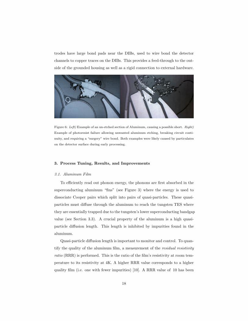
Figure 6: Left) Example of an un-etched section of Aluminum, causing a possible short. Right)
Example of photoresist failure allowing unwanted aluminum etching, breaking circuit conti-
nuity, and requiring a “surgery” wire bond. Both examples were likely caused by particulates
on the detector surface during early processing.
3. Process Tuning, Results, and Improvements
3.1. Aluminum Film
To efficiently read out phonon energy, the phonons are first absorbed in the
superconducting aluminum “fins” (see Figure 3) where the energy is used to
dissociate Cooper pairs which split into pairs of quasi-particles. These quasi-
particles must diffuse through the aluminum to reach the tungsten TES where
they are essentially trapped due to the tungsten’s lower superconducting bandgap
value (see Section 3.3). A crucial property of the aluminum is a high quasi-
particle diffusion length. This length is inhibited by impurities found in the
aluminum.
Quasi-particle diffusion length is important to monitor and control. To quan-
tify the quality of the aluminum film, a measurement of the residual resistivity
ratio (RRR) is performed. This is the ratio of the film’s resistivity at room tem-
perature to its resistivity at 4K. A higher RRR value corresponds to a higher
quality film (i.e. one with fewer impurities) [10]. A RRR value of 10 has been
18

deemed sufficient for a well functioning device in these detectors, but films have
been tuned using the SEGI to routinely achieve a value of ∼16.
3.2. Tc Tuning
Optimal detector readout relies on the TES sensors being held at specific
temperatures in their superconducting-transition resistance curves. The second
tungsten deposition forms the TES layer. Consequently, this deposition must
be carefully tuned to produce tungsten of a uniform, consistent, and precisely-
controlled critical temperature (Tc). Critical temperatures of thin tungsten
films are largely dictated by the ratio of α to β phase in the material. This
is due to the fact that the α-W exhibits a Tc of 15 mK [11] while β-W can
have Tc’s ranging from 1 to 4 K [12]. Utilizing this and the fact that the two
phases have different crystallographic structures (and therefore, different Bragg
angles), provides a technique of roughly estimating the Tc of a given sample at
room temperature using XRD[12] (see Figure 7). This technique is useful for
tuning film samples to have high α:β ratios (Tc’s closer to the desired range),
but in this range, the ratio becomes so heavily α-dominated that differences in
β concentrations become indistinguishable, making Tc predictions difficult. To
finely tune deposition parameters to the ∼80mK target, a dilution refrigerator
is used to physically measure the resistance transition as the sample is cooled
past its Tc and again as it warms up. With this feedback, depositions with
different sputtering power, substrate bias, and argon pressure were produced
and tested, creating films of varying Tc’s. In this process, a correlation was
established connecting room temperature resistivity of the films to their Tc
(see Figure 7, right), allowing recipes to be roughly tuned and chosen with
simple room temperature measurements (sheet resistance measured with a 4-
point probe, corrected for film thickness to calculate resistivity)[12]. Using
these processes, a recipe was chosen to produce films possessing the desired
Tc. Current experimentation with devices of varying Tc’s rely heavily on the
resistivity-Tc correlation, saving significant time and money required for dilution
refrigerator tests.
19

Figure 7: Left) XRD spectra showing discrimination between samples of differing α:β concen-
trations and their resulting Tc’s. Also marked are the locations of the peaks of pure α and β
phase films. An algorithm fitting two Gaussian functions (centered at these values) provides
an estimate of phase ratios, and therefore Tc’s, of the films. Right) Plot showing correlation of
critical temperature vs. sheet resistance of similar thickness films (40±4nm) [9]. These room
temperature characterization methods allow film deposition parameters to be tuned without
the time or monetary expense of dilution refrigerators (see Section 3.2).
In addition to depositing films with carefully tuned, repeatable Tc’s, the
SEGI has demonstrated the ability to produce films with much higher Tc uni-
formity across the substrate surface. Previous systems have had large Tc gradi-
ents across the face of detectors, beyond an acceptable limit (see Figure 8). To
correct this issue, Tc distributions must first be mapped (requiring detector test-
ing in a dilution refrigerator), followed by ion implantation of 56Fe (specifically
into the TES’s) to correct for the measured Tc gradient, a process described
in [13]. Films deposited in the SEGI, however, have demonstrated uniformi-
ties as good or better than typical post-implant samples from other systems.
This “as-delivered” uniformity circumvents a full round of millikelvin testing
(Tc mapping) and ion implantation, increasing throughput rates. The consis-
tency and uniformity of films produced by the SEGI may allow the test process
to largely avoid Tc testing, aside from periodic verification. Circuit continuity
tests can be accomplished at higher temperatures (up to ∼1K), meaning these
detectors may be able to avoid dilution refrigerator testing as a whole dur-
ing high throughput periods. With improved production throughput rates, the
20

bottleneck is shifted from fabrication to testing, exaggerating the importance of
these consistency and uniformity improvements.
Figure 8: Left) Example of W Tc variation (in mK) across a sample substrate face from
the previous CDMS deposition system. Middle) Tc variation of same film after ion implant
compensation (see Section 3.2). Figure adapted from [14]. Right) Tc measurements (see Table
2) from the 8 phonon channels of G9F, a detector fabricated at TAMU, demonstrating Tc
uniformity without ion implantation. All Tc’s are in mK.
3.3. Conformal Film Deposition
Controlling the fabrication quality of the aluminum-tungsten interface (to
maximize quasi-particle diffusion into the TES) is important because phonons
absorbed in the aluminum only contribute to the measured phonon signal if they
are able to drift into the tungsten. When quasi-particles drift from the aluminum
“fins” to the overlapping TES structure (see Figure 3), they must first drift into
the intermediate tungsten cap layer. Since this intermediate tungsten layer
is deposited immediately after the aluminum layer without breaking vacuum,
no oxide is able to form between the two. Without this cap layer, an oxide
forms on the aluminum surface before the TES layer deposition and inhibits
the diffusion of quasi-particles from one film to the other. While the cap layer
does oxidize slightly, the oxidation is easily removed with the RF etch which
precedes the TES film deposition, forming a more favorable interface between
the two tungsten layers.
The quasi-particle propagation from the “fins” to the TES’s is aided by the
bandgap disparity arising from the aluminum and tungsten films’ contrasting
21

Channel Tc (mK) Rn (Ω)
A1 75 0.64
B1 75 0.59
C1 77 0.59
D1 76 0.59
A2 75 0.69
B2 74 0.56
C2 73 0.54
D2 76 0.56
Table 2: Critical temperatures and “normal” resistance values (Rn) for the 8 phonon channels
of detector G9F (see Section 3.2). Rn is the resistance of the channel while the aluminum
is superconducting, but the tungsten is normal (held at a temperature significantly above its
Tc). Note: Channels A1 and A2 are outer channels (see Figure 8) and have higher Rn values
due to their sensor layout.
Tc’s (aluminum’s Tc of ∼1.2K equates to a gap energy of 0.18meV compared
to the tungsten’s gap energy of ∼ 25µeV)[9]. Due to the magnitude of disparity
in band gap energies, a process of quasi-particle multiplication can even occur
at this boundary[15].
Because it is deposited over an already etched structure, the TES film must
maintain continuity while stepping down ∼330nm (the initial aluminum + tung-
sten layer) from the initial tungsten cap layer to the a-Si layer. Discontinuity in
this region severs the phonon collection structure from the TES line (see Figures
3, 9, and 10), preventing signal readout. To avoid this issue, the TES film must
be a conformal layer closely following the topology, particularly the sidewall, of
the trilayer structures. This region is designated as the “waterfall” region (see
Figure 10 for examples of this feature exhibiting both poor and good continu-
ity). To prevent this problem, the “overhang etch” has been implemented into
the process. This etch was tuned by performing many iterations of circuit fabri-
cation on practice wafers with various overhang etch times using SEM imaging
for feedback. Once established, the process was confirmed with thick substrates,
22

again using SEM imaging.
Figure 9: Close-up and SEM image of “waterfall” boundary (see Section 3.3). Location on
phonon sensor and perspective are indicated by the arrow, referencing Figure 3.
Figure 10: Left) SEM images of overhang discontinuity issue. Middle) Conformal sidewall
deposition utilizing overhang etch, resulting in robust film continuity (see Section 3.3). Right)
SEM image of FIB-prepared cross-section of waterfall feature, showing conformal tungsten
deposition. FIB image courtesy of Evans Analytical Group.
3.4. a-Si Etch and “Trenching” of iZIP Detectors
Discrimination between background and signal events using these detectors
relies on a calibrated ratio of energy measured in the ionization channels ver-
sus that measured in the phonon channels. Charge carriers produced by events
near the faces of a detector often fail to drift through the entire crystal to the
appropriate electrode. This results in a reduced ionization collection signal,
causing the event to be improperly identified in subsequent analyses. A new
circuit design has been implemented to combat this. The design is called the
iZIP (interleaved Z-sensitive Ionization and Phonon detector)[16][17][18], and as
23

the name suggests, it utilizes interleaved electrodes on each surface. The inter-
leaved electrodes alternate from ground to +2V on one face and from ground
to -2V on the other (see Figure 11). This is in contrast to previous designs[1]
where one face is held at ground potential while the other is voltage biased. The
interleaved design produces a very uniform field in the bulk but local regions
of high field intensity near the surface. This causes the carriers (electrons and
holes) produced near the surface to both be collected by the adjacent surface,
with relatively little charge drifting to the opposite face. Therefore, any events
with significant disparities in charge collection from one face to the other (i.e.
failing the charge-symmetry requirement) are considered to be surface events.
This procedure has been demonstrated to be very successful and is the design
currently operating in SuperCDMS Soudan[19]. To fully realize the potential
of this technique, detectors should be able to hold higher biases (producing
stronger local surface fields) without breakdown. Limitations arise, however, as
the electrode spacing is ∼1mm, and current begins to leak across the surface as
voltage is increased, eventually resulting in breakdown. To reduce this problem
and allow higher bias voltage, a trench is etched into the surface of the sub-
strate, between the electrodes. For this purpose, the a-Si etch step is extended
by ∼700%. Because the gas used to etch the a-Si also etches the substrate mate-
rial, this extra time allows etching of the substrate itself. The process has been
tuned such that a trench of ∼1µm in depth is created between the electrodes
and has been shown[20] to produce detectors that can hold much higher bias
voltages without the problems mentioned previously (see Section 4).
3.5. Photoresist Studies
The tuning of the photoresist layer is of utmost importance as it dictates
not only the geometries of the final detector circuit structure, but whether or
not the deposited films survive the fabrication process at all. For this reason,
much time was spent investigating the photoresist layer and photolithographic
processing of this layer. The cross-section of the developed photoresist pattern
is controlled with the UV exposure, which can result in angled sidewalls (inward
24

+2V charge0V phonon
0V phonon-2V charge
Ge
iZIP Charge Signal
• Surface events (alpha, betas, nuclei) have 1-sided charge collection
• Bulk events (gammas, nuclear recoils) have 2-sided charge collection
• Charge symmetry is a powerful tag of surface events on top and bottom sides
• Noise limits usefulness of charge to > 8 keVnr
Z
R
+V 0V +V 0V +V 0V
-V 0V -V 0V -V 0V
Thursday, March 28, 13
~1mm
4
Figure 11: Left) Diagram of iZIP detector geometry/design used in SuperCDMS Soudan
showing alternating biased charge collecting rails and 0V phonon rails (see Section 3.4). Figure
from [19]. Right) Simulation of iZIP internal field lines, showing strong tangential electric fields
at the surface and a uniform drift field in the detector bulk, a method proven to discriminate
against the previously problematic surface events. Figure from [21].
or outward), changing the width of the film etched below (see Figure 12). A
dedicated study of the UV exposure (varying UV power and time, with SEM
feedback) was performed to prevent these problems from affecting our circuit
features.
In previous CDMS detector designs, Shipley Microposit S1813 photoresist[22]
has been used for the photolithographic processing. This chemical was chosen
for multiple reasons:
1. Resistance to etchant chemicals used in this process
2. Ability to reproduce sub-micron line-widths
3. Viscosity to match our desired layer thickness (∼1.4µm) with rotational
speeds that produce optimum uniformity (3500-5500rpm [22])
4. Compatibility with metal ion-free developers [22]
However, as substrates of larger mass joined the production line, it became
desirable to decrease spin coating speeds (causing less strain on the spin coater
and less risk to the substrates). For this reason, Shipley Microposit S1811[22]
is now used for its lower viscosity while still possessing the other characteristics
25

Figure 12: SEM image of a photoresist feature’s cross-section. Due to improper UV exposure,
this feature’s sidewalls angle outwards, protecting a wider area of film from etching underneath,
resulting in widening of circuit features. Note: This layer’s thickness of 1.66µm corresponds
to a previous spin coat recipe, using S1813 photoresist (see Section 3.5).
mentioned above. Using S1811, the spin coat process is performed at 2300 rpm
(as opposed to 4000 rpm required for S1813) for 60 seconds, producing a 1.4µm
layer on each face. These parameters (along with those of the UV exposure
mentioned previously) were tuned using feedback from SEM images confirming
faithful reproduction of mask feature line-widths and robust cross-sections after
exposure and development.
Another photoresist issue that was studied and successfully remedied is that
of a so-called “edge bead”. After the spin coat process, a thick bead of pho-
toresist can be seen around the edge of the substrate surface. Thicker than the
26

nominal layer, this bead does not receive enough UV exposure and developing
to be properly patterned/removed prior to etching. While there are no vital cir-
cuit features in this region, it prevents any films underneath from being etched
away, leaving a metal band (which could potentially cause shorts) around the
edge of the detector after the photoresist is removed. It is for this reason that
the previously mentioned shadow mask is implemented, preventing deposition
in this region (see Section 2.6). This procedure has proven to be a low cost yet
highly effective method of combating the edge bead problem, with negligible
impact on detector patterning at radial extremities.
4. Results to Date
Using this process at the dedicated TAMU fabrication facility, detectors have
been produced of the size and design of those in SuperCDMS Soudan. Test data
from detector G9F, one of the first of these produced at TAMU, can be seen
in Figure 13, demonstrating pulses from operational phonon sensor channels as
well as the 356 keV photopeak from a Ba-133 calibration source. In addition,
this detector showed unparalleled TES Tc uniformity without ion implant com-
pensation (see Figure 8 and Table 2). However, it showed an inability to hold
adequate bias voltage, leading to further tuning of the trenching process (see
Section 3.4). The following detector, G10F (using the improved trenching pro-
cess), demonstrated more than adequate ability to hold bias, showing no signs of
leakage up to ±5V (the limit of the test stand). Specification standards used to
rate SuperCDMS detectors categorize this detector as “very good”. Subsequent
testing showed functional charge performance up to 9V [20], much higher than
required for the experiment.
Detectors produced at this facility have demonstrated performance that
meets or exceeds the requirements for this experiment, certifying this location
as an integral fabrication facility for SuperCDMS SNOLAB detectors. 100 mm
x 33.3 mm thick science quality detectors were successfully produced at this
facility in early 2013 (see Figure 14) and are currently awaiting testing.
27

Figure 13: Left) Phonon pulses from detector G9F, fabricated at TAMU. Right) Calibration
spectrum from detector G9F, clearly showing the 356 keV Ba133 peak (see Section 4).
5. Conclusion
A robust, repeatable fabrication procedure has been established, demon-
strated, and improved at the TAMU fabrication facility. Increased throughput
as well as improvements made in the process itself are expected to contribute
substantially to the success of the next generation SuperCDMS SNOLAB exper-
iment. In particular, increased fabrication efficiency, improved TES Tc consis-
tency and uniformity, increased bias voltage ability due to substrate trenching,
and improved signal collection from overhang studies will improve detector suc-
cess rates, reducing fabrication and testing costs.
6. Acknowledgments
The authors would like to thank the CDMS team at SLAC/Stanford (es-
pecially Blas Cabrera, Paul Brink, Richard Partridge, Matt Cherry, Astrid
Tomada and John Mark Kreikebaum), Sunil Golwala, Betty Young, Jae Woo
Suh, the CDMS team at the University of Minnesota (especially Hassan Cha-
gani, Priscilla Cushman, Matt Fritts, Tommy Hofer, Allison Kennedy, Vuk
Mandic, Roxanne Radpour, David Strandberg, and Anthony Villano), and
the University of California, Berkeley 75 µW dilution refrigerator test team.
28

Figure 14: 100mm x 33.3mm detectors fabricated at TAMU, currently awaiting testing.
This work was supported by the Department of Energy (Contracts DE-FG02-
13ER41918, DE-AC03-76SF00098, DE-FG02-92ER40701, DE-FG02-94ER40823,
and DE-SC0004022), the National Science Foundation (Grant Nos. PHY-1102842
and NSF-0919599), and funding from Texas A&M University.
References
[1] D. S. Akerib, J. Alvaro-Dean, M. S. Armel-Funkhouser, M. J. Attisha,
L. Baudis, D. A. Bauer, J. Beaty, P. L. Brink, R. Bunker, S. P. Burke,
et al., First results from the Cryogenic Dark Matter search in the Soudan
Underground Laboratory, Physical Review Letters 93 (21) (2004) 211301.
[2] CDMS II Collaboration, et al., dark matter search results from the CDMS
II experiment, Science 327 (5973) (2010) 1619–1621.
[3] J. Sander, Z. Ahmed, A. J. Anderson, S. Arrenberg, D. Balakishiyeva, R. B.
Thakur, D. A. Bauer, D. Brandt, P. L. Brink, R. Bunker, et al., Super-
CDMS status from Soudan and plans for SNOLab, in: WORKSHOP ON
29

DARK MATTER, UNIFICATION AND NEUTRINO PHYSICS: CETUP*
2012, Vol. 1534, AIP Publishing, 2013, pp. 129–135.
[4] B. E. Warren, X-ray Diffraction, Dover Publications, Mineola, NY, USA,
1990.
[5] P. J. Holmes, P. Handler, The electrochemistry of semiconductors, Journal
of The Electrochemical Society 109 (8) (1962) 228C–228C.
[6] P. Brink, Z. Ahmed, D. Akerib, C. Bailey, D. Balakishiyeva, D. Bauer,
J. Beaty, R. Bunker, B. Cabrera, D. Caldwell, et al., Supercdms detec-
tor fabrication advances, in: THE THIRTEENTH INTERNATIONAL
WORKSHOP ON LOW TEMPERATURE DETECTORSLTD13, Vol.
1185, AIP Publishing, 2009, pp. 655–658.
[7] P. Brink, A. Anderson, D. Balakishiyeva, D. Bauer, J. Beaty, D. Brandt,
B. Cabrera, H. Chagani, M. Cherry, J. Cooley, et al., Detector fabrication
yield for supercdms soudan, Journal of Low Temperature Physics (2014)
1–7.
[8] K. R. Williams, R. S. Muller, Etch rates for micromachining processing,
Microelectromechanical Systems, Journal of 5 (4) (1996) 256–269.
[9] K. Prasad, Search for lightly ionizing particles using CDMS-II data and
fabrication of cdms detectors with improved homogeneity in properties,
Ph.d. Dissertation, Texas A&M University.
[10] C. James, The residual resistance of metals, Physics Education 2 (6) (1967)
315.
[11] E. Lassner, W.-D. Schubert, Tungsten: properties, chemistry, technology
of the elements, alloys, and chemical compounds, Springer, 1999.
[12] A. E. Lita, D. Rosenberg, S. Nam, A. J. Miller, D. Balzar, L. M. Kaatz,
R. E. Schwall, Tuning of tungsten thin film superconducting transition
30

temperature for fabrication of photon number resolving detectors, Applied
Superconductivity, IEEE Transactions on 15 (2) (2005) 3528–3531.
[13] B. A. Young, T. Saab, B. Cabrera, J. J. Cross, R. M. Clarke, R. A. Abu-
saidi, Measurement of Tc suppression in tungsten using magnetic impuri-
ties, Journal of Applied Physics 86 (12) (1999) 6975–6978.
[14] GEODM S4 Review, CDMS Internal Note.
[15] N. E. Booth, Quasiparticle trapping and the quasiparticle multiplier, Ap-
plied physics letters 50 (5) (1987) 293–295.
[16] M. Pyle, Optimizing the design and analysis of cryogenic semiconductor
dark matter detectors for maximum sensitivity, Ph.d. Dissertation, Stan-
ford University.
[17] P. L. Brink, B. Cabrera, J. P. Castle, J. Cooley, L. Novak, R. W.
Ogburn, M. Pyle, J. Ruderman, A. Tomada, B. A. Young, J. Filip-
pini, P. Meunier, N. Mirabolfathi, B. Sadoulet, D. N. Seitz, B. Serfass,
K. M. Sundqvist, D. S. Akerib, C. N. Bailey, M. R. Dragowsky, D. R.
Grant, R. Hennings-Yeomans, R. W. Schnee, First test runs of a
dark-matter detector with interleaved ionization electrodes and phonon
sensors for surface-event rejection, Nuclear Instruments and Methods
in Physics Research Section A: Accelerators, Spectrometers, Detec-
tors and Associated Equipment 559 (2) (2006) 414 – 416, proceedings
of the 11th International Workshop on Low Temperature Detectors
LTD-11 11th International Workshop on Low Temperature Detectors.
doi:http://dx.doi.org/10.1016/j.nima.2005.12.026.
URL http://www.sciencedirect.com/science/article/pii/
S0168900205024162
[18] M. Pyle, B. Serfass, P. L. Brink, B. Cabrera, M. Cherry, N. Mirabolfathi,
L. Novak, B. Sadoulet, D. Seitz, K. M. Sundqvist, et al., Surface electron
rejection from ge detector with interleaved charge and phonon channels,
31

in: The Thirteenth International Workshop on Low Temperature Detec-
torsLTD13, Vol. 1185, AIP Publishing, 2009, pp. 223–226.
[19] R. Agnese, A. J. Anderson, D. Balakishiyeva, R. B. Thakur, D. A. Bauer,
A. Borgland, D. Brandt, P. L. Brink, R. Bunker, B. Cabrera, et al., Demon-
stration of surface electron rejection with interleaved germanium detectors
for dark matter searches, Applied Physics Letters 103 (16) (2013) 164105.
[20] B. Shank, D. Q. Nagasawa, B. Cabrera, M. Cherry, B. A. Young, Charge
transport asymmetry in cryogenic high purity germanium, Journal of Low
Temperature Physics (2014) 1–7doi:10.1007/s10909-014-1111-y.
URL http://dx.doi.org/10.1007/s10909-014-1111-y
[21] S. Hertel, Advancing the search for dark matter: from CDMS II to Super-
CDMS, Ph.d. Dissertation, Massachusetts Institute of Technology.
[22] Shipley, Shipley Microposit S1800 Series Photo Resists Data Sheet (May
2012).
URL http://nanofab.ece.cmu.edu/resources/
s1800seriesDataSheet.pdf
32