CRKIT R5 Clock Architecture WINLAB – Rutgers University June 13, 2013 Khanh Le.
17
CRKIT R5 Clock Architecture WINLAB – Rutgers University June 13, 2013 Khanh Le
-
Upload
ralph-mccoy -
Category
Documents
-
view
217 -
download
2
Transcript of CRKIT R5 Clock Architecture WINLAB – Rutgers University June 13, 2013 Khanh Le.

CRKIT R5Clock Architecture
WINLAB – Rutgers University
June 13, 2013
Khanh Le

Zedboard Zynq System Clock Overview
PS PL33.333MHzref clock
(IC18, PS_CLK)
F7
4 programmable PL clocks
100MHzref clock
(IC17, GCLK)
Y9
For portability, use the 100MHz reference clock for PL section(will require one PLL)
ref_clk_out (RF ref clock ~30MHz)B19, B20
L18, L19 dac_clk_in (dac ref clock)
dac_clk_out (dac source synchronous clock)E19, E20
D18, C19 adc_clk_in (adc source synchronous clock)
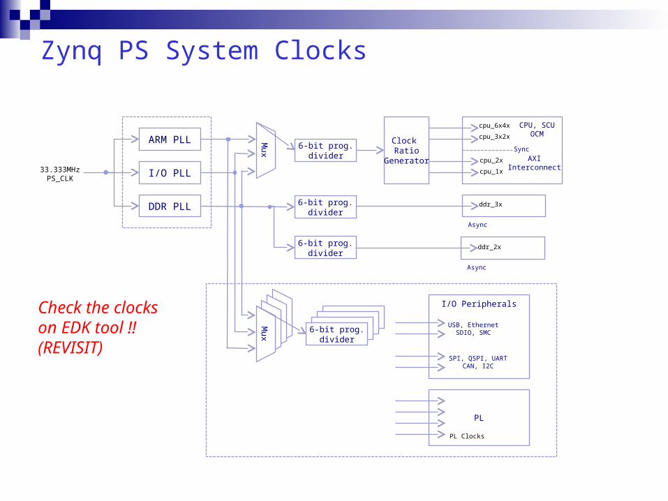
Zynq PS System Clocks
ARM PLL
33.333MHzPS_CLK
I/O PLL
DDR PLL
Mu
x
6-bit prog.divider
6-bit prog.divider
6-bit prog.divider
Mu
x
Clock Ratio
Generator
cpu_6x4x
cpu_3x2x
cpu_2x
cpu_1x
CPU, SCUOCM
AXIInterconnect
ddr_3x
ddr_2x
Sync
Async
Async
6-bit prog.divider
I/O Peripherals
USB, EthernetSDIO, SMC
SPI, QSPI, UARTCAN, I2C
PL
PL Clocks
Check the clockson EDK tool !!(REVISIT)

RF Interface
dac_data_out[15:0]
dac_clk_out
dac_frame_out (unused)
Not used for word-level, only forByte- or Nibble-level
AD9122DAC
AD9548Clock Sync
AD9523Clock Gen
AD9643ADC
dac_clk_in
ref_clk_out(~30MHz)
Jitter clean up
adc_data_in[13:0]
adc_clk_in
adc_or_in
IQ
10
LVDS
CMTPLL
ODDR(SAME_EDGE Mode)
clock feedback
DAC Interface
RF Reference Clock
ADC Interface
I2C Interface
@tx_clk
CMTMMCM
CTL REG
Programmableref. clock(ug472)
100MHz
RxBaseband
D1D2 Q
D1D2
Q
By default, +Rising edge = I +Falling edge = Q
+Twos complement
Anti-aliasing filter cut-off @125MHz -> Nyquist sampling rate @250MHz
IQ
Q1Q2 D
IDDR(SAME_EDGE_PIPELINED Mode)
CMTMMCM
@125MHz
clock feedback
scl
sdata I2C -> SPIPCORE
INT REG
@125MHz
Sampling RateDown Conversion
Clock domain crossing. Must support fractional synchronization e.g. 125MHz -> 20MHz
TxBaseband
Sampling RateUp Conversion
By default, +Rising edge = I +Falling edge = Q
+Twos complement+ ~1ns skew between data and DCO
(DCO delay vs data)
@prog_rx_clk
For fractional clock divider
CLKOUT1
CLKOUT0
@100MHzsys_clk
M=3, D=2, O1=5
M=3, D=2, O0=1.5
CLKOUT1
CLKOUT0
NOT NEEDED(no clock deskew)
CLKOUT0
CLKOUT1
@prog_tx_clk
REVISIT : do we need interpolation in the framework ? Or use the DAC for interpolation ?
Answer – interpolation within Framework.(Up/Down conversion not critical at this point)

ODDR Timing

IDDR Timing

DAC Timing
DAC Register MapDefault
Data bus sampling point is nominally 350ps after each edge of DCI signal, with uncertainty of +/- 300 ps.
Data interface timing can be verified using the Sample Error Detection (SED) circuitry (reg 0x07, 0x67-0x73).
Reference : AD9122_DAC.pdf
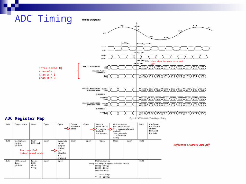
ADC Timing
ADC Register Map
Interleaved IQ channels :Chan A = I Chan B = Q
Reference : AD9643_ADC.pdf
~1ns skew between data and DCO
For parallel interleaved mode
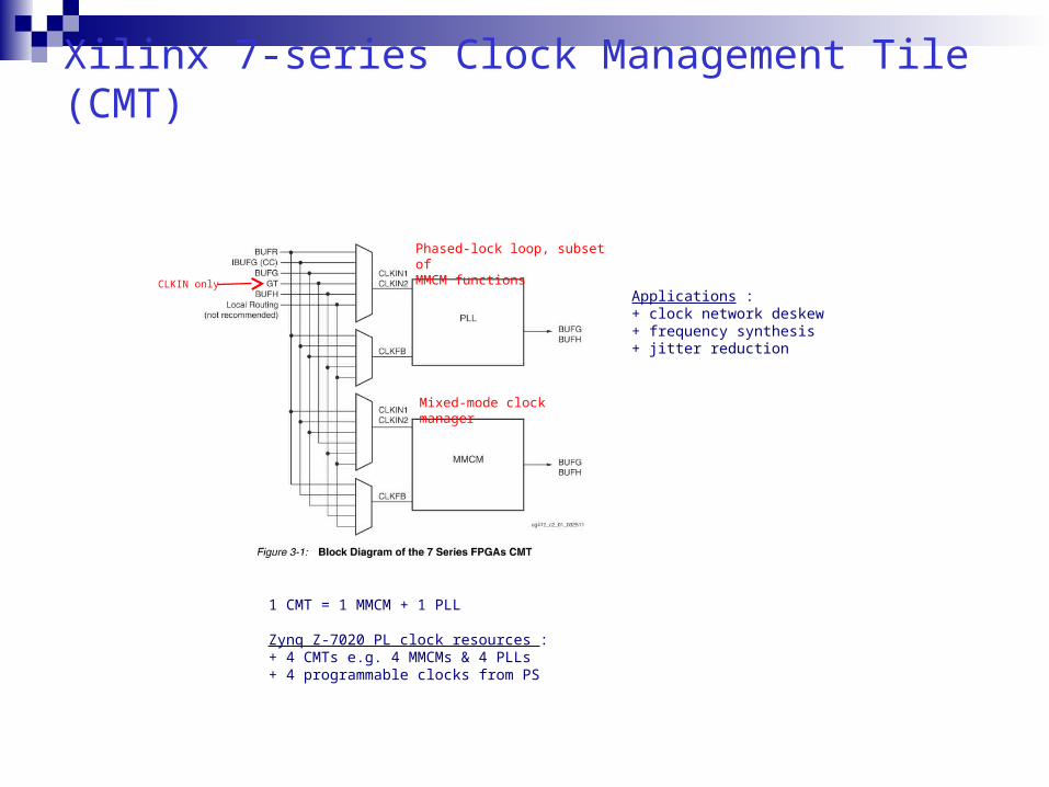
Xilinx 7-series Clock Management Tile (CMT)
Mixed-mode clock manager
Phased-lock loop, subset of MMCM functions
1 CMT = 1 MMCM + 1 PLL
Zynq Z-7020 PL clock resources : + 4 CMTs e.g. 4 MMCMs & 4 PLLs+ 4 programmable clocks from PS
CLKIN onlyApplications : + clock network deskew+ frequency synthesis+ jitter reduction

CMT - MMCM
Programming port(ug472 + xapp888)
Integercounter
Independent clock control
FractionalcounterWith Fclkin = 100MHz, M=1, D=1 :
Integer divide :O0 = 1 : Fout = 100MHzO1 = 2 : Fout = 50MHzO2 = 3 : Fout = 33.33MHzO3 = 4 : Fout = 25MHzO4 = 5 : Fout = 20MHzO5 = 6 : Fout = 16.66MHz
Fout = 80MHz, then O0 = Fclkin/Fout = 100/80 = 10/8 = 1.25 (fractional divide).Fout = 30MHz, O0 = 100/30 = 3.3333…
Alternative,M=3, D=2, O1=5 : CLKOUT1 = 30MHz (rf ref clock)M=3, D=2, O0=1.5 : CLKOUT0 = 100MHz (system clock)
With Fclkin = 125MHz (ADC sync clock), M=1, D=1 :Fout = 80MHz, O0 = 125/80 = 1.5625Fout = 20MHz, O0 = 125/20 = 6.25
Attributes : M = CLKFBOUT_MULT_F D = DIVCLK_DIVIDEO = CLKOUT_DIVIDE(ug472, page 79)

CMT - PLL
Integer onlycounter
Programming port
Attributes : M = CLKFBOUT_MULT_F D = DIVCLK_DIVIDEO = CLKOUT_DIVIDE

MMCM and PLL Use Models (ug472, page 87)
Requires two BUFGsRequires only one BUFG+ jitter filtering+ frequency synthesis+ no phase requirement between Fin and Fout
Off-chip compensation
Input buffers must be in same bank.
Use COREGEN to get additional settings information.

Clock Network Deskew Restrictions
Restrictions for feedback :
Fin Fout
FFB
Example 1 :Fin = 166MHz, D = 1, M = 6, O = 2
FVCO = M x FFB = M x (FIN / D) FVCO = 6 x 166MHz = 996MHz and FOUT = FVCO / O = 996MHz / 2 = 498 MHz
1
6
2
Fin Fout
FFB
30
4
Example 2 :Fin = 66.66MHz, D = 2, M = 30, O = 4
FVCO = M x FFB = M x (FIN / D) = 30 x (66.66MHz / 2) = 999.9MHz ~ 1000MHzandFOUT = FVCO / O = 1000MHz / 4 = 250 MHz
2
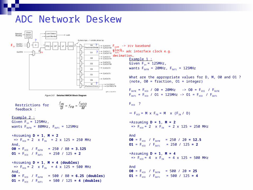
ADC Network Deskew
Restrictions for feedback :
Fin Fout0 -> rcv baseband clock
FFB
Example 1 :Given Fin = 125MHz,wants FOUT0 = 20MHz, FOUT1 = 125MHz
What are the appropriate values for D, M, O0 and O1 ?(note, O0 = fraction, O1 = integer)
FOUT0 = FVCO / O0 = 20MHz -> O0 = FVCO / FOUT0 FOUT1 = FVCO / O1 = 125MHz -> O1 = FVCO / FOUT1
FVCO ?
FVCO = M x FFB = M x (FIN / D)
+Assuming D = 1, M = 2 => FVCO = 2 x FIN = 2 x 125 = 250 MHz
AndO0 = FVCO / FOUT0 = 250 / 20 = 12.5O1 = FVCO / FOUT1 = 250 / 125 = 2
+Assuming D = 1, M = 4 => FVCO = 4 x FIN = 4 x 125 = 500 MHz
AndO0 = FVCO / FOUT0 = 500 / 20 = 25O1 = FVCO / FOUT1 = 500 / 125 = 4
?
?
? Fout1 -> adc interface clock e.g. decimation…
Example 2 :Given Fin = 125MHz,wants FOUT0 = 80MHz, FOUT1 = 125MHz
+Assuming D = 1, M = 2 => FVCO = 2 x FIN = 2 x 125 = 250 MHz And,O0 = FVCO / FOUT0 = 250 / 80 = 3.125O1 = FVCO / FOUT1 = 250 / 125 = 2
+Assuming D = 1, M = 4 (doubles) => FVCO = 2 x FIN = 4 x 125 = 500 MHz And,O0 = FVCO / FOUT0 = 500 / 80 = 6.25 (doubles)O1 = FVCO / FOUT1 = 500 / 125 = 4 (doubles)
?

Clock Distribution e.g. Zedboard Zynqhow many APP can be supported ?

Interpolation/Decimation – Rational Sampling Rate Converters
SAVE FOR LATER ! NOT CRITICAL AT THIS POINT

Clock Domain Abstraction Layers
MOVE TO SEPARATE DESIGN DOCUMENT !