Cosmic Ray Detector - Modifications and Completion
28
Cosmic Ray Detector - Modifications and Completion U of S Subatomic Physics Internal Report SPIR-136 Christopher Little 24th August 2005 Contents 1 Previous Work 2 2 Theory 3 2.1 Background ............................... 3 2.2 Coincidence Detection Circuitry .................... 4 3 Detector Support Structure 6 3.1 Pre-existing Support Structure ..................... 6 3.2 Secondary Support Ring ........................ 7 3.3 Table and Main Ring Modifications .................. 8 4 Circuit Problems and Modifications 9 4.1 Initial Circuitry Status .......................... 9 4.2 Power Supply Modifications ...................... 10 4.3 Circuit Board Modifications ...................... 10 5 Circuit Box Fabrication and Further Circuit Board Modifications 11 5.1 Circuit Box Fabrication ......................... 11 5.2 Circuit Board Modifications ...................... 12 6 Threshold Voltages 13 6.1 Data Acquisition ............................ 13 6.2 Threshold Setting ............................ 14 7 Software 15 7.1 Existing Software ............................ 15 7.2 New Software .............................. 16 7.2.1 Basic Layout and Design Requirements ............ 16 7.2.2 Communication with Pre-Existing Software .......... 17 7.2.3 Initializing the Display Window ................ 17 1
Transcript of Cosmic Ray Detector - Modifications and Completion
Cosmic Ray Detector - Modifications andCompletion
U of S Subatomic Physics Internal Report SPIR-136
Christopher Little
24th August 2005
Contents
1 Previous Work 2
2 Theory 32.1 Background . . . . . . . . . . . . . . . . . . . . . . . . . . . . . . . 32.2 Coincidence Detection Circuitry . . . . . . . . . . . . . . . . . . . . 4
3 Detector Support Structure 63.1 Pre-existing Support Structure . . . . . . . . . . . . . . . . . . . . . 63.2 Secondary Support Ring . . . . . . . . . . . . . . . . . . . . . . . . 73.3 Table and Main Ring Modifications . . . . . . . . . . . . . . . . . . 8
4 Circuit Problems and Modifications 94.1 Initial Circuitry Status . . . . . . . . . . . . . . . . . . . . . . . . . . 94.2 Power Supply Modifications . . . . . . . . . . . . . . . . . . . . . . 104.3 Circuit Board Modifications . . . . . . . . . . . . . . . . . . . . . . 10
5 Circuit Box Fabrication and Further Circuit Board Modifications 115.1 Circuit Box Fabrication . . . . . . . . . . . . . . . . . . . . . . . . . 115.2 Circuit Board Modifications . . . . . . . . . . . . . . . . . . . . . . 12
6 Threshold Voltages 136.1 Data Acquisition . . . . . . . . . . . . . . . . . . . . . . . . . . . . 136.2 Threshold Setting . . . . . . . . . . . . . . . . . . . . . . . . . . . . 14
7 Software 157.1 Existing Software . . . . . . . . . . . . . . . . . . . . . . . . . . . . 157.2 New Software . . . . . . . . . . . . . . . . . . . . . . . . . . . . . . 16
7.2.1 Basic Layout and Design Requirements . . . . . . . . . . . . 167.2.2 Communication with Pre-Existing Software . . . . . . . . . . 177.2.3 Initializing the Display Window . . . . . . . . . . . . . . . . 17
1

7.2.4 Updating the Display Window . . . . . . . . . . . . . . . . . 187.2.5 Suggested Upgrades . . . . . . . . . . . . . . . . . . . . . . 19
8 Assembly Instructions 19
9 Finished Product 20
10 References 21
A Dimensioned Drawings and Sketches of Components Fabricated by thePhysics Machine Shop 22
B Diagram of the Detection Circuitry 27
C Appropriate Threshold Voltages for Specific Detectors 27
D Calibration Procedure 28
1 Previous Work
This cosmic ray detector was originally commissioned as a fourth year design project atthe University of Saskatchewan. Group members Amanda Gerbrandt, Nolan Dougherty,and Janelle McKenzie submitted their final report to the supervising professor Rob Py-well on March 29, 2004. See [DGM].
At the completion of the design group’s efforts with the detector, its status was asfollows:
12 scintillator-photomultiplier tube (PMT) detectors were acquired and a standwas built to house 8 of them.
The circuitry necessary for detecting a coincidence between detectors was builtand tested in a wire-wrap circuit.
The interface and software for sending event data through a parallel port to aLinux-operated PC was designed, programmed, and tested.
There were problems with the polling and interface timings and while the logiccircuit and software could operate independently, they were not compatible, andthe circuit could not supply event data to the computer directly.
The detector was then passed to the summer students Micheal Barnett, Jennifer Robb,and Ward Wurtz for completion. The steps they took toward the completion of thedetector array were:
Re-thinking and simplifying the existing circuit logic.
Designing and ordering a printed circuit board to eliminate the stray capacitancethat was affecting the coincidence logic.
2

Improving the existing software and file-system for gathering information andpurchasing a more aesthetically pleasing monitor (a 17 inch flat-panel monitor).
Eliminating the polling and interface timing problems through the aforemen-tioned improvements to the software and circuit logic.
Designing and building a high voltage distribution box so that all the detectorscould be powered by one power supply.
Purchasing a power supply/AC-DC converter so that the circuitry could be runfrom power outlets in the building.
For a more in-depth view of these improvements and modifications please refer to[BRW].
2 Theory
2.1 Background
Cosmic rays are high-energy charged particles traveling at nearly the speed of lightthat constantly bombard the earth from all directions. Any subatomic charged particleoriginating from outside earth’s atmosphere can be considered a cosmic ray. Whencosmic rays strike the earth’s atmosphere they collide with the nuclei of atoms suchas nitrogen and oxygen creating many subatomic particles such as muons and pions inwhat is known as a cosmic ray shower (see figure 1). Muons are of particular interestin the detection of cosmic rays, as they decay much more slowly (µs order) than otherhigh energy particles and they are able to pass through large amounts of material sincethey have no strong interaction properties. These muon characteristics make them thebest means of detecting when a cosmic ray has hit the atmosphere.
3
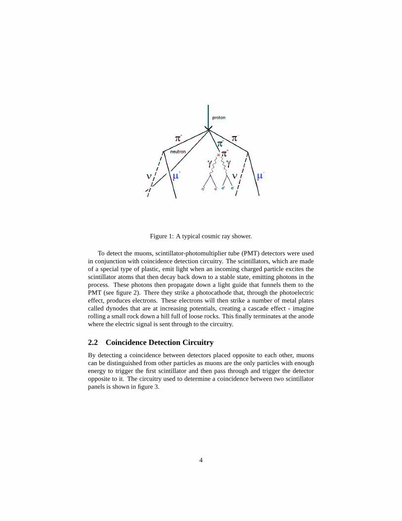
Figure 1: A typical cosmic ray shower.
To detect the muons, scintillator-photomultiplier tube (PMT) detectors were usedin conjunction with coincidence detection circuitry. The scintillators, which are madeof a special type of plastic, emit light when an incoming charged particle excites thescintillator atoms that then decay back down to a stable state, emitting photons in theprocess. These photons then propagate down a light guide that funnels them to thePMT (see figure 2). There they strike a photocathode that, through the photoelectriceffect, produces electrons. These electrons will then strike a number of metal platescalled dynodes that are at increasing potentials, creating a cascade effect - imaginerolling a small rock down a hill full of loose rocks. This finally terminates at the anodewhere the electric signal is sent through to the circuitry.
2.2 Coincidence Detection Circuitry
By detecting a coincidence between detectors placed opposite to each other, muonscan be distinguished from other particles as muons are the only particles with enoughenergy to trigger the first scintillator and then pass through and trigger the detectoropposite to it. The circuitry used to determine a coincidence between two scintillatorpanels is shown in figure 3.
4
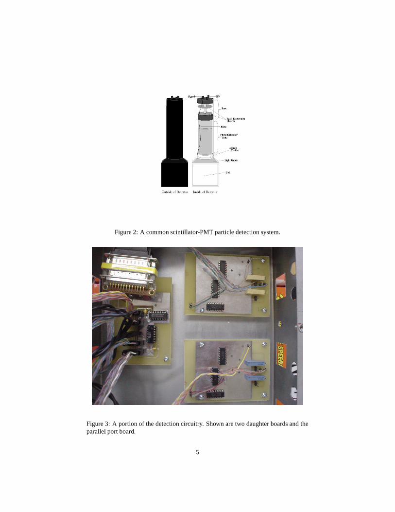
Figure 2: A common scintillator-PMT particle detection system.
Figure 3: A portion of the detection circuitry. Shown are two daughter boards and theparallel port board.
5
Discriminator
Discriminator
Multivibrator Flip Flop
Computer
Board 2
Board 3
Board 4
PMT
PMT
−5 V
−5 V
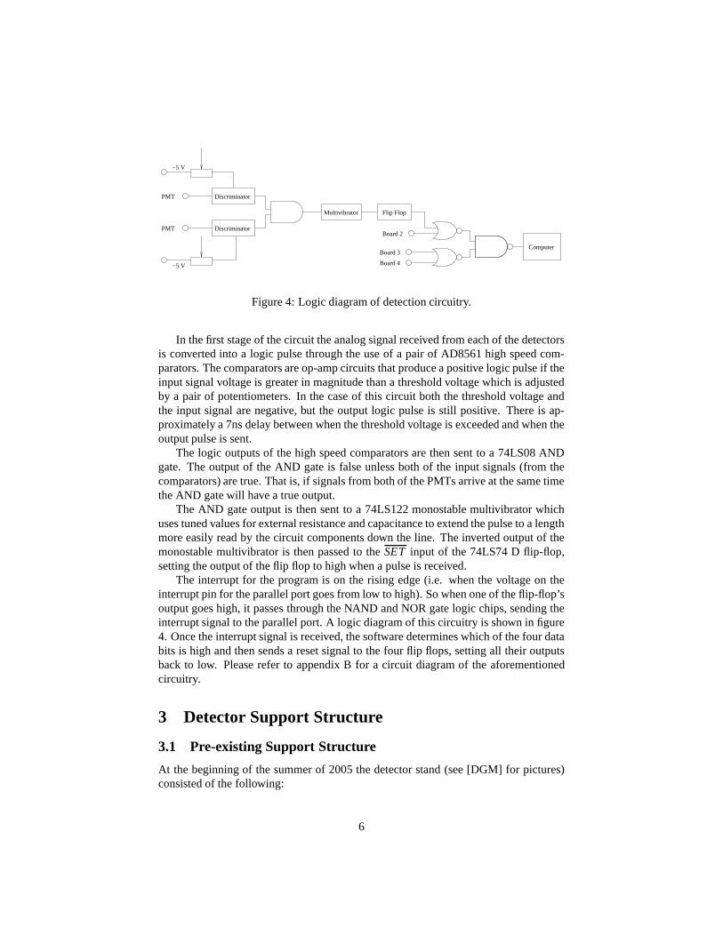
Figure 4: Logic diagram of detection circuitry.
In the first stage of the circuit the analog signal received from each of the detectorsis converted into a logic pulse through the use of a pair of AD8561 high speed com-parators. The comparators are op-amp circuits that produce a positive logic pulse if theinput signal voltage is greater in magnitude than a threshold voltage which is adjustedby a pair of potentiometers. In the case of this circuit both the threshold voltage andthe input signal are negative, but the output logic pulse is still positive. There is ap-proximately a 7ns delay between when the threshold voltage is exceeded and when theoutput pulse is sent.
The logic outputs of the high speed comparators are then sent to a 74LS08 ANDgate. The output of the AND gate is false unless both of the input signals (from thecomparators) are true. That is, if signals from both of the PMTs arrive at the same timethe AND gate will have a true output.
The AND gate output is then sent to a 74LS122 monostable multivibrator whichuses tuned values for external resistance and capacitance to extend the pulse to a lengthmore easily read by the circuit components down the line. The inverted output of themonostable multivibrator is then passed to the SET input of the 74LS74 D flip-flop,setting the output of the flip flop to high when a pulse is received.
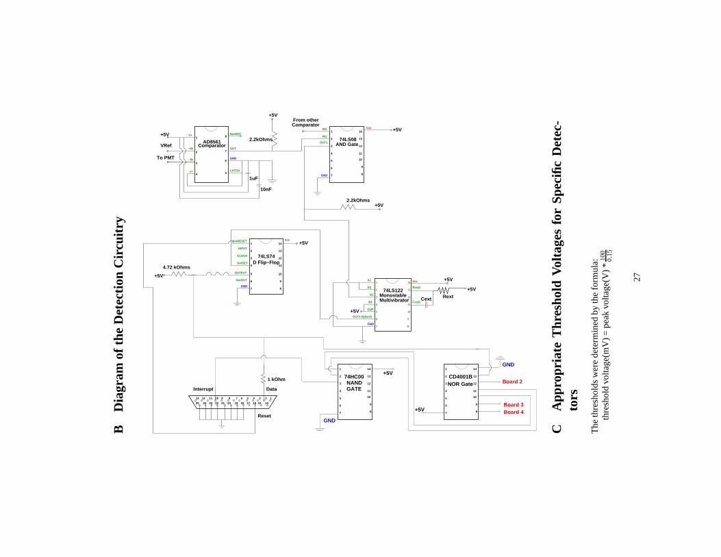
The interrupt for the program is on the rising edge (i.e. when the voltage on theinterrupt pin for the parallel port goes from low to high). So when one of the flip-flop’soutput goes high, it passes through the NAND and NOR gate logic chips, sending theinterrupt signal to the parallel port. A logic diagram of this circuitry is shown in figure4. Once the interrupt signal is received, the software determines which of the four databits is high and then sends a reset signal to the four flip flops, setting all their outputsback to low. Please refer to appendix B for a circuit diagram of the aforementionedcircuitry.
3 Detector Support Structure
3.1 Pre-existing Support Structure
At the beginning of the summer of 2005 the detector stand (see [DGM] for pictures)consisted of the following:
6
A table with a hole in the center for the detectors.
A main ring to support the detectors mounted to the table.
There were three major areas of concern about this original stand assembly. First,the detectors were not supported in the scintillator (flat panel) area and as a resultsnapped under their own weight. Second, the stand itself was not very stable, causingconcern as the combined weight of the detectors put a considerable load on this stand.Finally, installation and removal of the detectors was problematic as they all needed tobe removed or installed at the same time with the previous design.
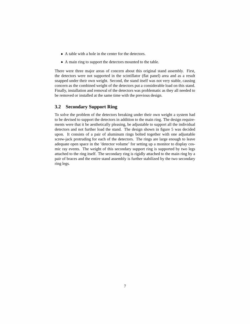
3.2 Secondary Support Ring
To solve the problem of the detectors breaking under their own weight a system hadto be devised to support the detectors in addition to the main ring. The design require-ments were that it be aesthetically pleasing, be adjustable to support all the individualdetectors and not further load the stand. The design shown in figure 5 was decidedupon. It consists of a pair of aluminum rings bolted together with one adjustablescrew-jack protruding for each of the detectors. The rings are large enough to leaveadequate open space in the ’detector volume’ for setting up a monitor to display cos-mic ray events. The weight of this secondary support ring is supported by two legsattached to the ring itself. The secondary ring is rigidly attached to the main ring by apair of braces and the entire stand assembly is further stabilized by the two secondaryring legs.
7
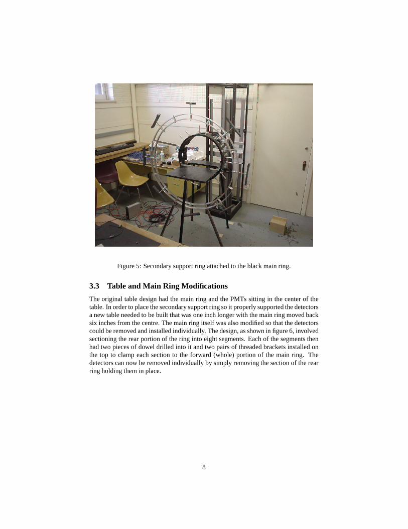
Figure 5: Secondary support ring attached to the black main ring.
3.3 Table and Main Ring Modifications
The original table design had the main ring and the PMTs sitting in the center of thetable. In order to place the secondary support ring so it properly supported the detectorsa new table needed to be built that was one inch longer with the main ring moved backsix inches from the centre. The main ring itself was also modified so that the detectorscould be removed and installed individually. The design, as shown in figure 6, involvedsectioning the rear portion of the ring into eight segments. Each of the segments thenhad two pieces of dowel drilled into it and two pairs of threaded brackets installed onthe top to clamp each section to the forward (whole) portion of the main ring. Thedetectors can now be removed individually by simply removing the section of the rearring holding them in place.
8
Figure 6: Modified main ring with a sectioned rear ring for easy detector removal.
4 Circuit Problems and Modifications
4.1 Initial Circuitry Status
At the beginning of the summer the circuits and parallel port were all connected to-gether but the computer was not receiving the coincidence signals from the detectioncircuitry. The following problems were observed:
The flip flops would go high when they received data, but the computer didn’treceive the signal and therefore didn’t send the reset signal to set the flip flopsback to low.
The 74HC00 NAND gate was not hooked up properly according to its data sheet.
Some of the potentiometers that adjusted the threshold voltage of the discrimina-tors had an output voltage that drifted and the would sometimes output a positive
9
voltage.
The parallel port and circuit boards’ ground was different from the LPT24 5Vpower supply’s ground.
The 5V power supply was outputting irregular voltages along the +5V line.
Throughout the summer the above problems were investigated and corrected.
4.2 Power Supply Modifications
The first problem addressed with the power supply was the irregular voltage outputalong the 5V power line. After the proper documentation was found it was discoveredthat the 5V power line had to output at least 300mA of current to work properly. As thecircuit components are all high impedance, this presented a problem since the circuitsthemselves didn’t draw enough current. To overcome this problem an 80 Ohm 2 Wattresistor was added in parallel to the circuits and a steady 5V output was achieved
To solve the grounding problem a three pronged power cord was soldered ontothe power supply on the AC input end. Then a wire going from the AC ground (thebuilding’s ground) was soldered on to the common of the DC output end. Now the DCoutput’s ground is the same as the building’s ground which is the same as the parallelport’s ground resulting in all the circuitry being properly grounded and powered.
4.3 Circuit Board Modifications
Initially it was thought that the reason that the computer was not receiving the eventdata was because somewhere along the line a component had been damaged. Sincethe NAND gate wasn’t working properly it was replaced and bypass capacitors wereinstalled to protect the ICs from future damage due to irregularities in the power linefeed. After this installation the computer still wasn’t receiving the signal from thecircuitry. Upon closer inspection it was discovered that for the rising edge of the flipflip output to trigger the interrupt, the NAND gate and the 4001b NOR gate would haveto be switched. This explained why the computer was not receiving the interrupt andwhy the NAND gate was hooked up improperly. The socket that it had been occupyingwas, in fact, meant for the NOR gate.
At this point it was discovered that one of the data lines for the parallel port boardwas always set at high, even if no daughter board was hooked up to it. A quick referenceto the pin assignment for the enhanced parallel port showed that this data line washooked up to pin one which was the the write pin of the EPP and would always behigh. This data line was then disconnected from pin one and hooked up to pin 5 whichwas one of the four data pins from which the data acquisition software reads.
The potentiometers’ positive output and drifting problems were due to an intrinsicbias current on the discriminator input for the threshold line. If the discriminators wereworking properly this bias current should have shut off when a voltage was suppliedalong the threshold line. Upon replacing one of the discriminators, it was discoveredthat this anomalous behavior started only when the potentiometer was driven to its
10

extremes (that is 0 or 200 kΩ). It was, therefore, concluded that driving the poten-tiometers to their extremes damaged the discriminators and caused them to output abias current even if there was a voltage along the threshold line. To avoid future prob-lems with the discriminators it is important to ensure that the potentiometers are notnear their extremes when powering up the circuit. Also, if the boards should sometimeundergo further modifications or are redesigned, a 50Ω resistor should be attached tothe ground end of the potentiometers to prevent them from ever going down to 0Ω.These changes along with the above-mentioned power supply modifications resultedin working detection circuitry from which the data acquisition software could receivedata.
5 Circuit Box Fabrication and Further Circuit BoardModifications
5.1 Circuit Box Fabrication
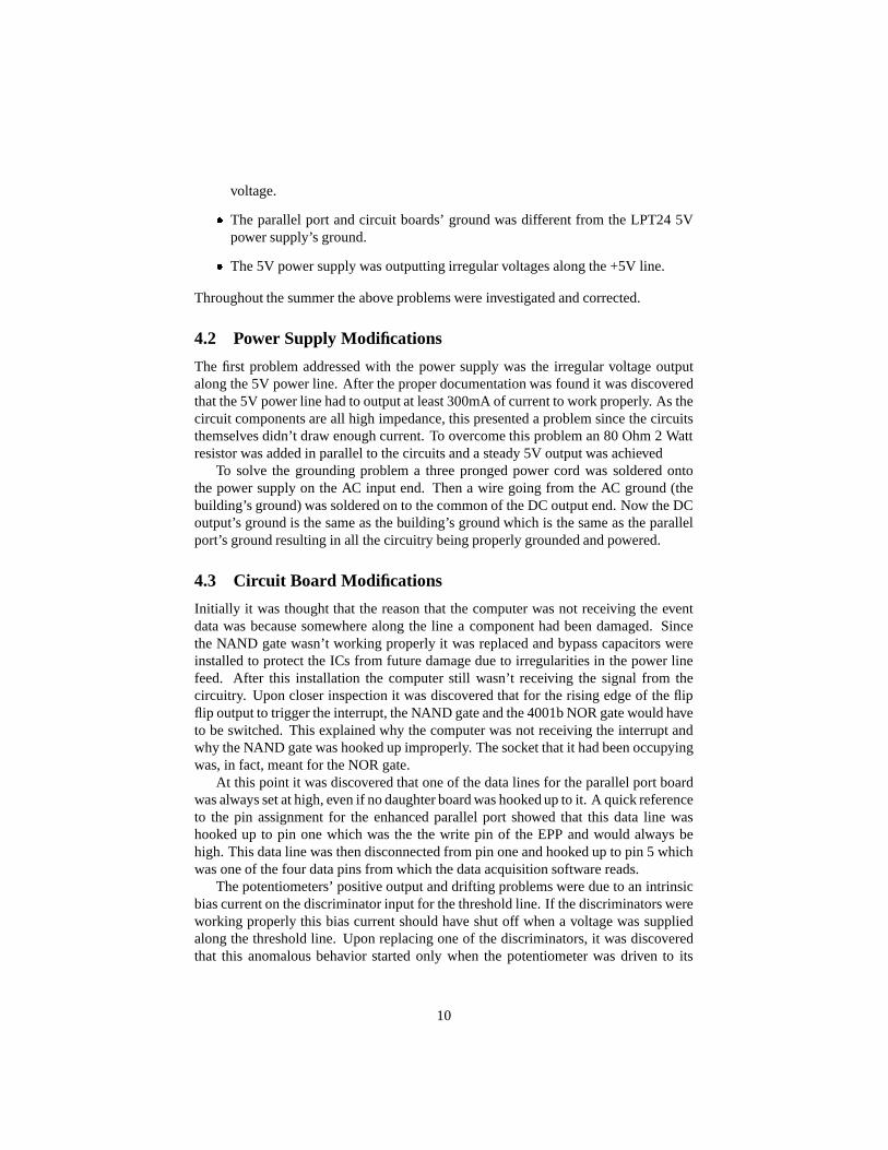
For protection and convenience, the circuit box, as shown in figure 7, was designed tohouse all of the circuitry and the power supply in a rigid container. The circuits are tobe convection cooled and the square holes on the top and bottom sides were punchedout to provide airflow. BNC bulkhead connectors were also installed to allow the boxto be moved without removing the individual PMT signal inputs from the daughterboards, as well as to make it easier to put an oscilloscope in parallel to the circuit forthreshold voltage testing. This box will be mounted underneath the bottom screw-jackon the secondary support ring with a plexiglas cover to further protect the circuits.
11
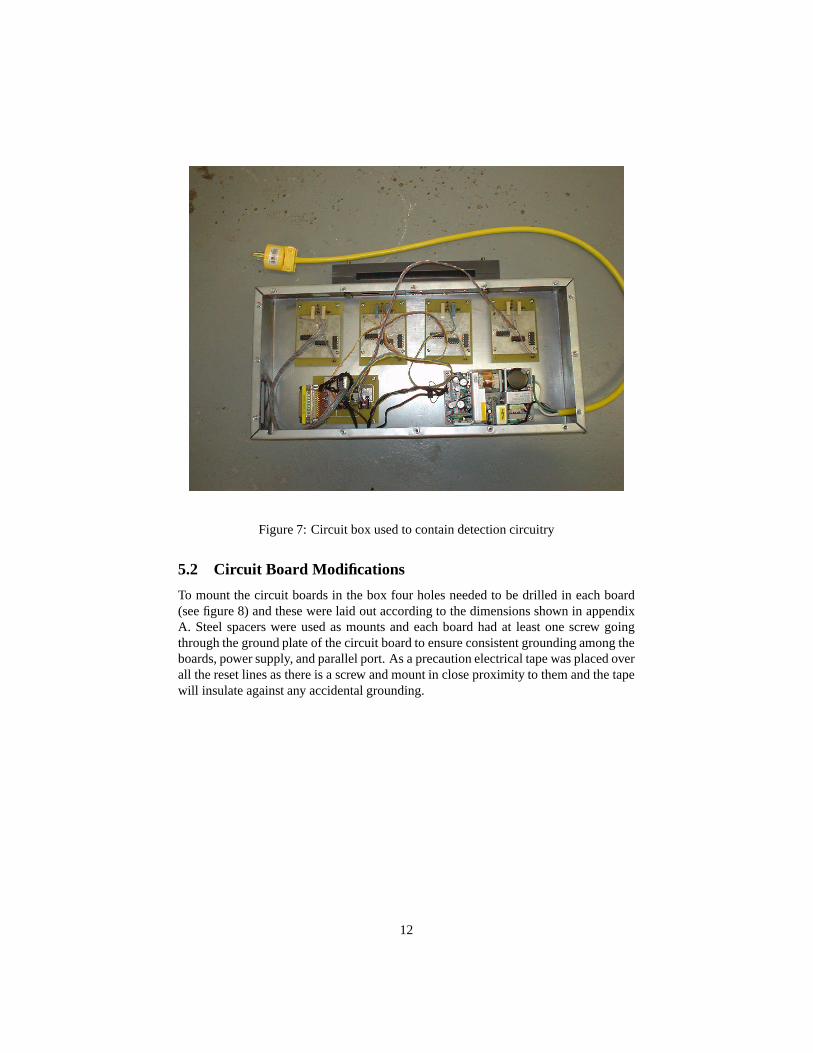
Figure 7: Circuit box used to contain detection circuitry
5.2 Circuit Board Modifications
To mount the circuit boards in the box four holes needed to be drilled in each board(see figure 8) and these were laid out according to the dimensions shown in appendixA. Steel spacers were used as mounts and each board had at least one screw goingthrough the ground plate of the circuit board to ensure consistent grounding among theboards, power supply, and parallel port. As a precaution electrical tape was placed overall the reset lines as there is a screw and mount in close proximity to them and the tapewill insulate against any accidental grounding.
12
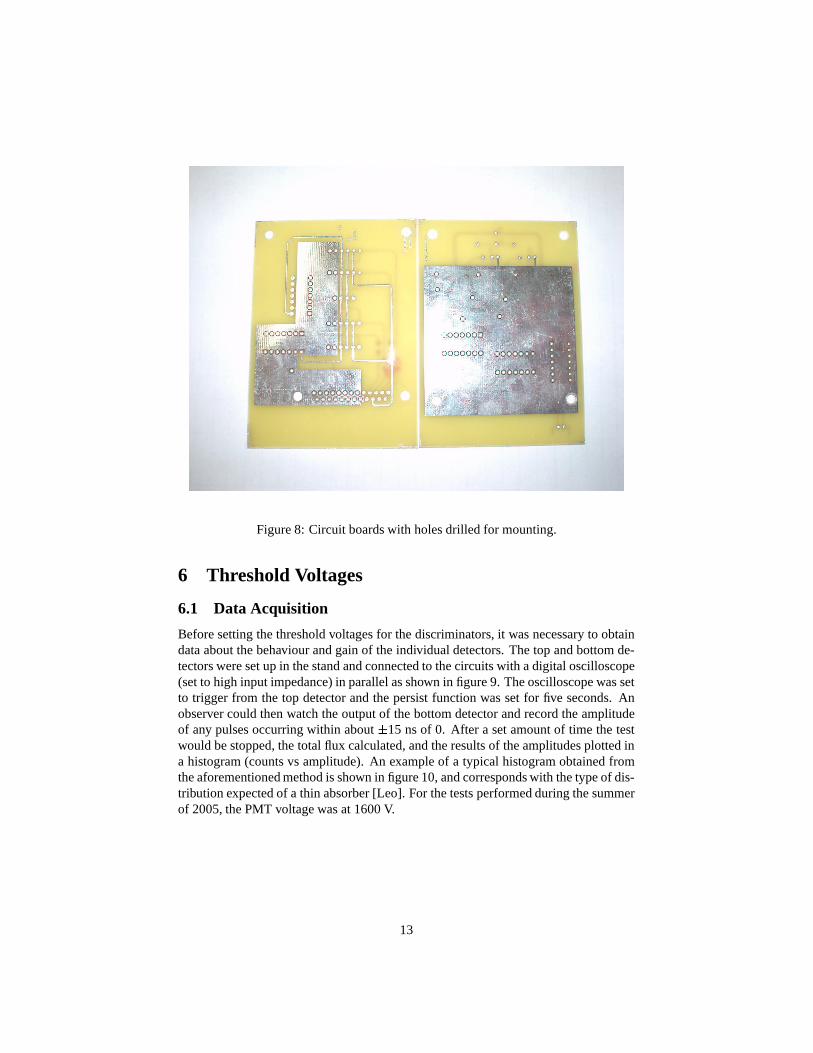
Figure 8: Circuit boards with holes drilled for mounting.
6 Threshold Voltages
6.1 Data Acquisition
Before setting the threshold voltages for the discriminators, it was necessary to obtaindata about the behaviour and gain of the individual detectors. The top and bottom de-tectors were set up in the stand and connected to the circuits with a digital oscilloscope(set to high input impedance) in parallel as shown in figure 9. The oscilloscope was setto trigger from the top detector and the persist function was set for five seconds. Anobserver could then watch the output of the bottom detector and record the amplitudeof any pulses occurring within about
15 ns of 0. After a set amount of time the test
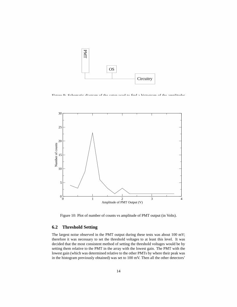
would be stopped, the total flux calculated, and the results of the amplitudes plotted ina histogram (counts vs amplitude). An example of a typical histogram obtained fromthe aforementioned method is shown in figure 10, and corresponds with the type of dis-tribution expected of a thin absorber [Leo]. For the tests performed during the summerof 2005, the PMT voltage was at 1600 V.
13
OS
PMT
Circuitry
Figure 9: Schematic diagram of the setup used to find a histogram of the amplitudesoutput by a detector.
0 1 2 3 4Amplitude of PMT Output (V)
0
5
10
15
20
25
30
Num
ber
of c
ount
s
Figure 10: Plot of number of counts vs amplitude of PMT output (in Volts).
6.2 Threshold Setting
The largest noise observed in the PMT output during these tests was about 100 mV;therefore it was necessary to set the threshold voltages to at least this level. It wasdecided that the most consistent method of setting the threshold voltages would be bysetting them relative to the PMT in the array with the lowest gain. The PMT with thelowest gain (which was determined relative to the other PMTs by where their peak wasin the histogram previously obtained) was set to 100 mV. Then all the other detectors’
14
discriminators were set to a threshold voltage that was appropriate for the their relativegain. For example, detectors seven and nine both had their histogram peaks at 150mV- which corresponds to the lowest gain in the array - so the thresholds for the discrim-inator’s connected to these detectors were set at 100 mV. On the other hand, the peakfor detector two was 300mV; therefore its discriminators’ threshold was set at 200 mV.This method resulted in some valid coincidences being discarded from the detectorswith higher gains, but it ensured that all of the detectors had the same sensitivity as theleast sensitive detector. It is important to note that even though the histograms wereobtained at a PMT voltage of 1600 V, the thresholds are independent of the PMT volt-age as they are all relative to the 100mV threshold set on the PMT with the lowest gain.The noise seems to be independent of PMT voltage.
7 Software
7.1 Existing Software
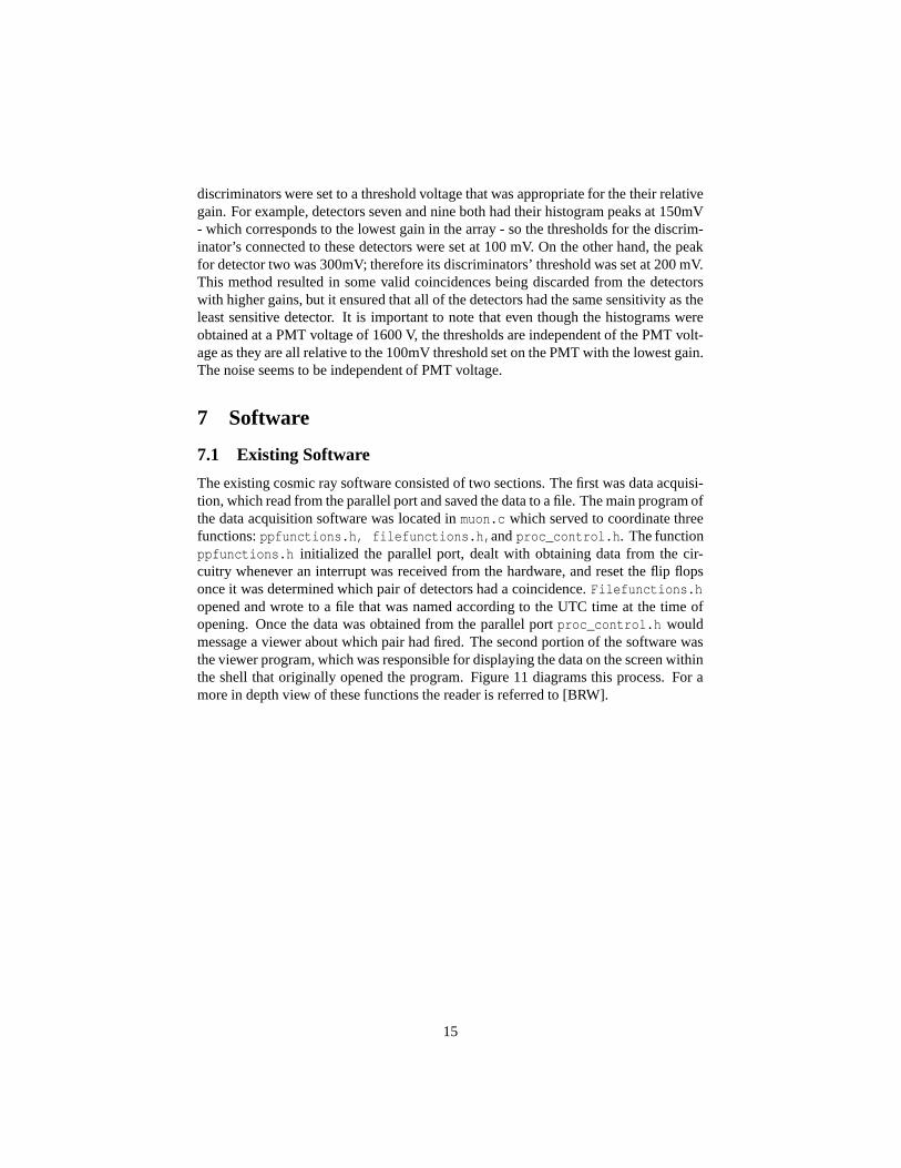
The existing cosmic ray software consisted of two sections. The first was data acquisi-tion, which read from the parallel port and saved the data to a file. The main program ofthe data acquisition software was located in muon.c which served to coordinate threefunctions: ppfunctions.h, filefunctions.h,and proc_control.h. The functionppfunctions.h initialized the parallel port, dealt with obtaining data from the cir-cuitry whenever an interrupt was received from the hardware, and reset the flip flopsonce it was determined which pair of detectors had a coincidence. Filefunctions.hopened and wrote to a file that was named according to the UTC time at the time ofopening. Once the data was obtained from the parallel port proc_control.h wouldmessage a viewer about which pair had fired. The second portion of the software wasthe viewer program, which was responsible for displaying the data on the screen withinthe shell that originally opened the program. Figure 11 diagrams this process. For amore in depth view of these functions the reader is referred to [BRW].
15
start
save data to file
init parallel port
start viewer
open file
message viewer
close parallel port
close file
halt viewer
block forparallel portor signal
parallelport
end
programdid the
unblock?
why
signal
Figure 11: Flow chart of the pre-existing software.
7.2 New Software
7.2.1 Basic Layout and Design Requirements
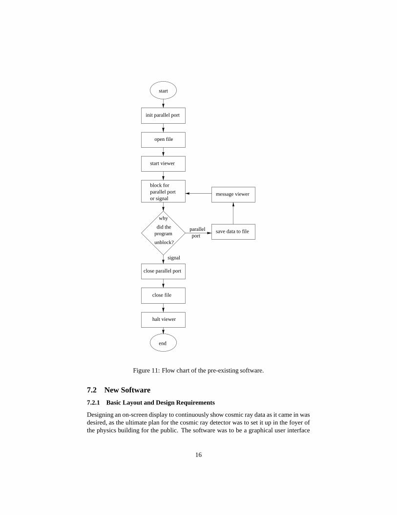
Designing an on-screen display to continuously show cosmic ray data as it came in wasdesired, as the ultimate plan for the cosmic ray detector was to set it up in the foyer ofthe physics building for the public. The software was to be a graphical user interface
16
(GUI) that could communicate with the existing software and display events in theform of histograms, pictures, and text. A GUI building program called Glade (GTK-based software) was used to make the basic layout of the GUI as shown in figure 12.The layout left room for three histograms: one displaying the angular distribution ofcosmic rays since the previous midnight, one displaying the number of cosmic rays inthe last twenty-four hours, and one displaying the number of cosmic rays in the presenthour. Also a picture window that has a picture of the last pair of detectors to fire, a textbox listing the coincidences, and a quit button were included.
Figure 12: Screen shot of the GUI’s original layout.
7.2.2 Communication with Pre-Existing Software
The pre-existing software is opened through the shell as it was previously, that is,muon.c is opened from the shell and it in turn opens viewer.c. To incorporate the GUIsoftware into the pre-existing software a popen()statement was included in viewer.c,which opens the GUI and creates a data pipe between the two programs. Wheneverthe viewer program has data, it prints it to the buffer in the pipe and the functiongdk_input_add()in the main.c portion of the GUI program calls the D_List call-back to deal with the data present in the buffer.
7.2.3 Initializing the Display Window
When the GUI is opened by viewer.c there is a series of initializations that must occurbefore the window is suitable for displaying cosmic ray data. First in main.c all of thesections of the GUI are assigned a pointer using the lookup_widget()function so thatthey can be referred to throughout the program. The graphics context is also defined
17
and most of the global variables are initialized in main.c. When the window opens anexpose_event callback is activated for the assigned sections and the axes for all thehistograms are drawn and labeled. More specifically the expose_event callback callsthe function Redraw.h which redraws the histogram, axes, and axes labels, but as nodata has been obtained yet only the axes and axes labels are drawn. The expose_eventcallback is also called whenever there is a change to one of the assigned sections of thewindow, such as resizing or putting another window in front of the GUI, ensuringthat the histograms and the picture window are always fully displaying the appropriatedata. The size of the histogram sections are obtained every time the expose_eventcallback is activated and each section is divided into a thirty by thirty-five grid for easyplacement of histogram bins, axes, and axes labels.
7.2.4 Updating the Display Window
As previously mentioned, whenever data is received from viewer.c the D_List call-back is activated. The D_List callback is responsible for updating all of the sectionsof the display window with new data whenever it is received. The data present in thebuffer is read to a string which is then converted to an integer and assigned to thevariable int which_pair. The integer will be a number ranging from one to fourinclusive with each number corresponding to a pair of detectors. First a text messageis appended to the text window displaying which detector pair has fired. Then thefunctions contained within histograms.h are called to update the histograms and thepicture window. The histograms.h functions keep a tally of their histogram’s binsand appends to them when there have been enough data entries to warrant increasingthat specific bin by one grid interval. Once the height of a bin crosses a certain thresh-old, set to be the maximum value on the y-axis, the maximum value is increased, they-axis relabeled, and the bins redrawn the the proper new height. For the “Numberof Cosmic Rays in the Last 24 Hours” histogram, the x-axis is labeled according towhat the local time is - using the system library time.h - and the bins are shifted oneto the left whenever the hour changes. The other two histograms also use the systemtime information to reset the “Number of Cosmic Rays Since Midnight as a Functionof Angle” plot every night at midnight and to reset the “Number of Cosmic Rays ThisHour” plot every hour. The display window of the GUI is shown in figure 13.
18
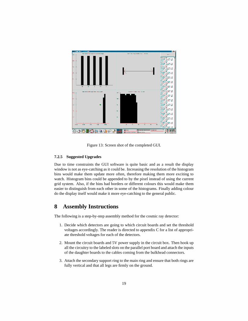
Figure 13: Screen shot of the completed GUI.
7.2.5 Suggested Upgrades
Due to time constraints the GUI software is quite basic and as a result the displaywindow is not as eye-catching as it could be. Increasing the resolution of the histogrambins would make them update more often, therefore making them more exciting towatch. Histogram bins could be appended to by the pixel instead of using the currentgrid system. Also, if the bins had borders or different colours this would make themeasier to distinguish from each other in some of the histograms. Finally adding colourdo the display itself would make it more eye-catching to the general public.
8 Assembly Instructions
The following is a step-by-step assembly method for the cosmic ray detector:
1. Decide which detectors are going to which circuit boards and set the thresholdvoltages accordingly. The reader is directed to appendix C for a list of appropri-ate threshold voltages for each of the detectors.
2. Mount the circuit boards and 5V power supply in the circuit box. Then hook upall the circuitry to the labeled slots on the parallel port board and attach the inputsof the daughter boards to the cables coming from the bulkhead connectors.
3. Attach the secondary support ring to the main ring and ensure that both rings arefully vertical and that all legs are firmly on the ground.
19

4. Put the detectors in their chosen slots and mount the circuit box under the bottomscrew-jack.
5. Hook up the voltage distribution box and run power lines to each of the detectors’high voltage (HV) power input.
6. Plug the BNC lines into the detectors’ output jacks which are opposite to the HVpower input (diagonal to the 800 V input), for the negative pulse output.
7. Attach the computer to the parallel port board and start the software at ~/Cosmi-cray_GUI/muon_cosmic_ray/muon.
8. Power up the detectors by slowly increasing the voltage of the HV power supply.
9. Run the BNC lines to the circuit box and plug them into the correct bulkheadconnectors.
During the assembly of the cosmic ray detector there are a few key issues that must bebrought to the attention of the reader:
Take care installing the detectors as the scintillators break easily.
While placing the circuit boards in their box make sure that the power is off andthat the mounts are not shorting out any of the circuit boards.
Ensure that all of the secondary support ring’s screw-jacks have felt betweenthem and the detectors.
Plug in the PMT output lines to the circuitry after the data acquisition programis running. This ensures that all of the flip-flops have been reset to low.
Make sure that the correct detector is hooked up to the correct circuit input.
Make sure that the potentiometers are not near their extremes when powering upthe circuit.
9 Finished Product
At the end of summer 2005 all the components were hooked together and workingproperly in the betatron lab. The only step remaining is constructing a display case andmoving the array, shown in figure 14, upstairs to the foyer for display.
20
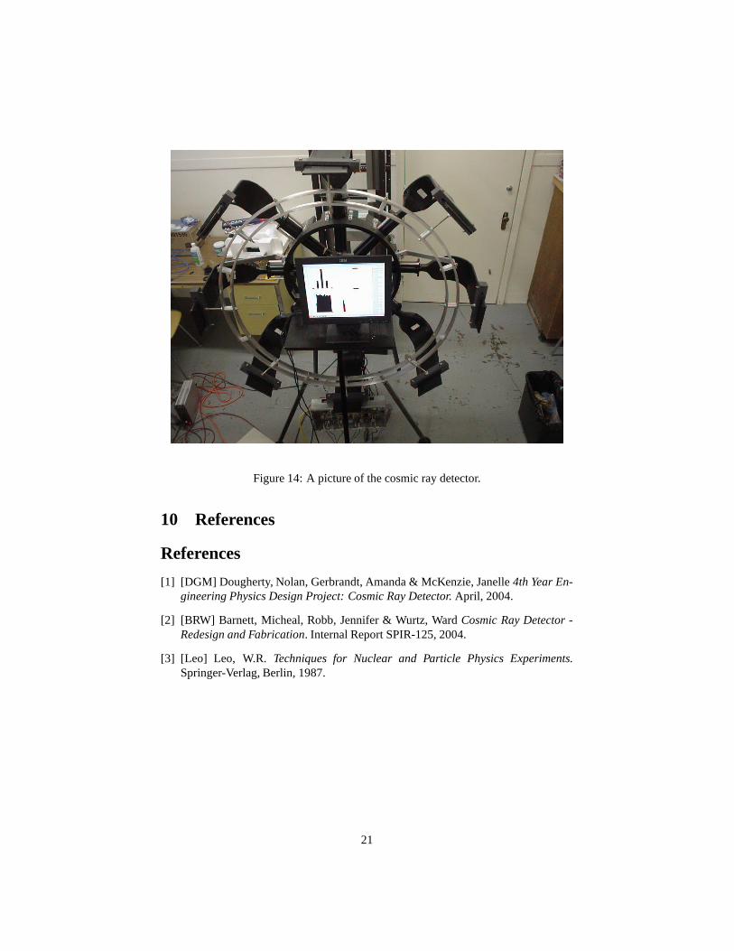
Figure 14: A picture of the cosmic ray detector.
10 References
References
[1] [DGM] Dougherty, Nolan, Gerbrandt, Amanda & McKenzie, Janelle 4th Year En-gineering Physics Design Project: Cosmic Ray Detector. April, 2004.
[2] [BRW] Barnett, Micheal, Robb, Jennifer & Wurtz, Ward Cosmic Ray Detector -Redesign and Fabrication. Internal Report SPIR-125, 2004.
[3] [Leo] Leo, W.R. Techniques for Nuclear and Particle Physics Experiments.Springer-Verlag, Berlin, 1987.
21
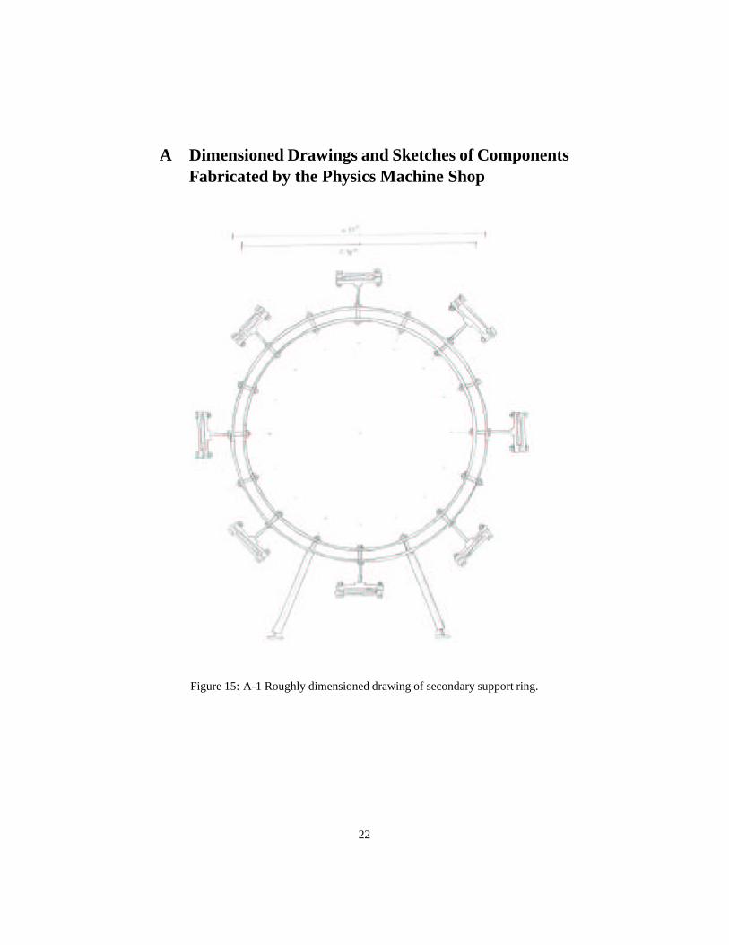
A Dimensioned Drawings and Sketches of ComponentsFabricated by the Physics Machine Shop
Figure 15: A-1 Roughly dimensioned drawing of secondary support ring.
22
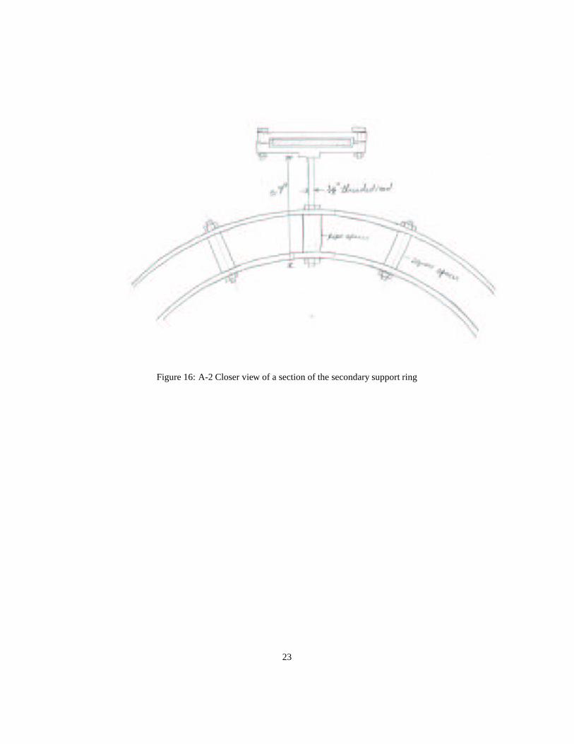
Figure 16: A-2 Closer view of a section of the secondary support ring
23
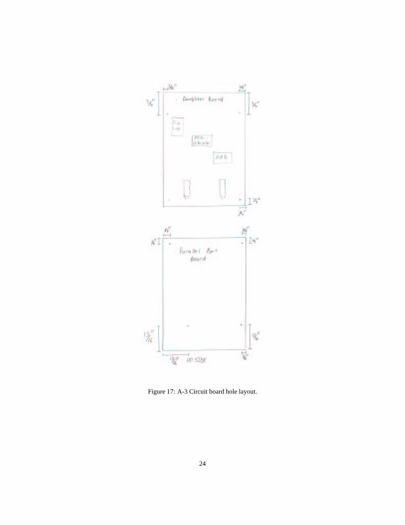
Figure 17: A-3 Circuit board hole layout.
24
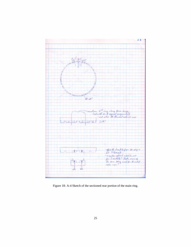
Figure 18: A-4 Sketch of the sectioned rear portion of the main ring.
25
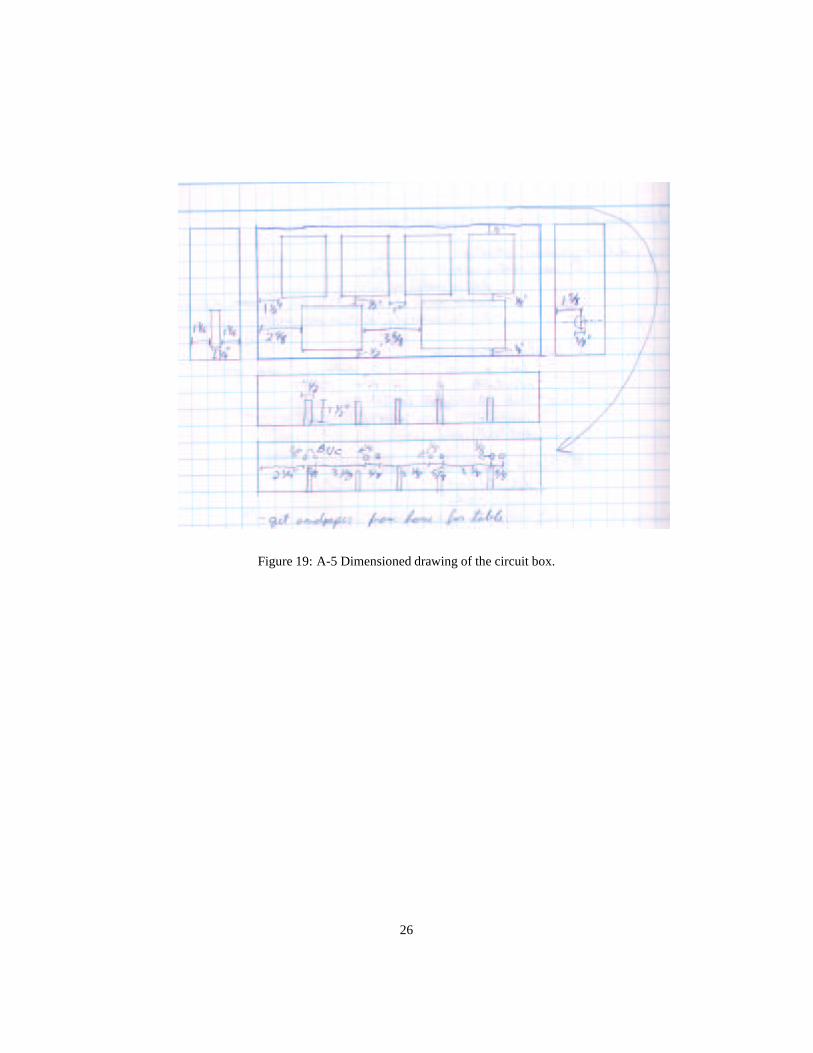
Figure 19: A-5 Dimensioned drawing of the circuit box.
26
BD
iagr
amof
the
Det
ecti
onC
ircu
itry
+5V
1
2
3
4
5
6
7
14
13
12
11
10
9
8
MultivibratorMonostable
74LS122
Vcc +5V
CLR
Rext2
Cext2
+5V
Cext Rext
+5VOUT2 (Qbar2)
GND
A1
A2
1
2
5
6
7 8
9
11
14
13
10
1
2
3
4
5
6
7
14
13
12
11
10
9
8
74LS08AND Gate
1
2
3
4
5
6
7
14
13
12
11
10
9
8
CD4001BNOR Gate
1
2
3
4
5
6
7
14
13
12
11
10
9
8
74HC00NANDGATE
+5V
10nF
From otherComparator
+5V
ComparatorAD8561
1
2
3
4
8
7
6
5
GND
GND
Vcc
V+
+IN
−IN
V− LATCH
OUT
NotOUT
OUT1
IN1
IN1
1uF
2.2kOhms
2.2kOhms
VRef
To PMT
+5V
74LS743
4
12
GND
Vcc
OUTPUT
NotOUT
CLOCK
INPUT
NotRESET
D Flip−FlopNotSET
+5V
4.72 kOhms
1 kOhm
Interrupt Data
Reset
11 10 2 11213 9 5678
1416171819202122232425 15
34
+5V
B2
B1
+5V
GND
Board 2
Board 3Board 4
+5V
GND
CA
ppro
pria
teT
hres
hold
Vol
tage
sfo
rSp
ecifi
cD
etec
-to
rs
The
thre
shol
dsw
ere
dete
rmin
edby
the
form
ula:
thre
shol
dvo
ltage
(mV
)=pe
akvo
ltage
(V)
*10
00
15
27

where:0.15V = the peak voltage of the detector in the array with the lowest gain100 mV = the threshold appropriate for the detector in the array with the lowest
gain
Detector # Peak Voltage (V) Threshold Voltage (mV)
2 0.3 2004 0.15 1005 0.0875 58.36 0.75 5007 0.15 1008 0.4 2669 0.15 10010 0.05 3312 0.3 20013 0.2 133
111 0.3 200333 1.25 833
Table 1: The peak voltage and threshold for each detector.
D Calibration Procedure
At the end of summer 2005, the number of cosmic rays typically detected by the arrayper hour was about 1300. If the cosmic ray detector eventually reports numbers thatare drastically different than this value there are a few things that should be checked.First, shut down the array and check the potentiometers’ output voltages and see if theyare still sufficiently close to the value recorded for the individual detectors in appendixC.
If the thresholds are still at the correct level there may be a light leak in the detector.To test for this remove the detector from the array and hook it up an oscilloscope.Then set the oscilloscope’s trigger to about -50 mV and cover the detector. Power upthe detector and slowly remove the cover, if the oscilloscope display suddenly turnsbrighter then a light leak is present and must be repaired.
If both of these tests fail to explain the reason for the anomalous readings thenthe detector may be broken or the gain could have shifted. To check if the gain hasshifted, the oscilloscope should be put in parallel with the circuit as shown in figure9. Then set up the oscilloscope and HV power supply as described in section 6 andrecord the amplitude of the PMT pulses. Once enough data is gathered to make anaccurate distribution determine at what the most common output amplitude is and seeif it corresponds to the value in appendix C. If the gain has shifted adjust the thresholdaccordingly.
28