Copyright by Gregory Blachut 2016
251
Copyright by Gregory Blachut 2016
Transcript of Copyright by Gregory Blachut 2016

Copyright
by
Gregory Blachut
2016
The Dissertation Committee for Gregory Blachut Certifies that this is the approved
version of the following dissertation:
Design of Silicon-containing Block Copolymer Materials for
Applications in Lithography
Committee:
Carlton Grant Willson, Supervisor
Christopher J. Ellison, Co-Supervisor
Venkat Ganesan
Chris A. Mack
Deji Akinwande
Design of Silicon-containing Block Copolymer Materials for
Applications in Lithography
by
Gregory Blachut, B.S.
Dissertation
Presented to the Faculty of the Graduate School of
The University of Texas at Austin
in Partial Fulfillment
of the Requirements
for the Degree of
Doctor of Philosophy
The University of Texas at Austin
December 2016

Dedication
This dissertation is dedicated to my parents, for their love and support.

v
Acknowledgements
I would like to thank Professor Grant Willson for being an extraordinary advisor
in all sense of the word. I would also like to thank my other advisor as well, Professor
Christopher Ellison, for his exceptional guidance throughout the years. Perhaps the
biggest testament to the character of both of these men lies in the droves of talented
students that flock to their groups. It has been my great honor to work alongside some of
these students throughout my years at UT, and to even call some of them my close
friends. I thank Michael Maher, Yusuke Asano, William Durand, Austin Lane, and
Sunshine Zhou for our close collaborations. In addition, I am graciously beholden to the
mentorship of Christopher Bates, Julia Cushen, Josh Katzenstein, William Bell, and Ryan
Deschner. I am also very fortunate to have worked with a number of eager and forgiving
undergraduates who also deserve thanks and recognition: Ziang Li, Adam Wrobel, Gary
Cantu, Andrew Dinhobl, and Paul Ortega. The administrative assistance and friendship of
Donna Martin, Kathleen Sparks, Mindy Maloney, and Kate Baird is also very
appreciated. Last, the sense of comradery from the rest of the Willson and Ellison group
members will be sorely missed.
I was very fortunate as well to have the opportunity to collaborate directly with
Lam Research and IMEC as part of this research. Diane Hymes, Stephen Sirard, Johan
Vertommen, David Hellin, Bart Coenegrachts, Mohand Brouri, Christophe Noben, Geert
Vandenberghe, Roel Gronheid, Paulina Rincon Delgadillo, BT Chan, Nadia
Vandenbroeck, Hari Pathangi, Arjun Singh, Robert Seidel, Jan Doise, Grant Garner,
Rikimaru Sakamoto, Yasanobu Someya, Hiroyuki Wakayama and many others

vi
contributed to this monumental effort. In addition, a different collaboration with Seagate
was made possible by XiaoMin Yang and Kim Lee.
Last, I would like to thank Dr. Justin Shearer for being my under-graduate
research mentor and enabling my jump to graduate school.

vii
Design of Silicon-containing Block Copolymer Materials for
Applications in Lithography
Gregory Blachut, Ph.D.
The University of Texas at Austin, 2016
Supervisor: C. Grant Willson
Co-supervisor: Christopher J. Ellison
Continual advancement in microelectronic performance has made
microelectronics essentially ubiquitous, enriching modern life in ways unimaginable even
a few decades ago. The advancement in microelectronic devices is made possible by
advancements in the manufacturing processes used to make them. Chief among these
technologies is lithography, the process by which the individual components on the
device are patterned. At present, complex and complicated double-patterning processes
are being used to extend the resolution of the lithographic methods used in high-volume
manufacturing, but only at great cost. Future generations of microelectronic devices will
require even further use of multiple-patterning processes, at which point the economics of
manufacturing could prevent the commercialization of such devices.
This economic reality has spurred interest in alternative patterning technologies.
One of the leading potential methods is to exploit the self-assembly of block copolymers
(BCPs). BCPs are a type of polymer consisting of two or more chemically distinct blocks
that are covalently joined together. The components of a BCP can phase-separate, and the
resultant features form on the 5 to 50 nm length-scale. This size range is coincidentally
ideal for next-generation semiconductor devices. However, BCPs on their own do not

viii
immediately form device-relevant features. Processes known collectively as directed self-
assembly (DSA) are needed to properly guide BCPs.
The work in this dissertation focuses on a very specific class of BCPs, those that
contain silicon in just one of the blocks. The presence of silicon in the molecule produces
many lithographic advantages, but also requires specialized processing steps. Chapter 1
provides an overview of lithography and block copolymer self-assembly. Chapter 2
introduces the materials and techniques needed to control the behavior of silicon-
containing BCPs. Chapter 3 presents and characterizes a variety of silicon-containing
BCPs. Last, Chapters 4 and 5 describe two implementations of silicon-containing BCP
DSA, one for semiconductor patterning, and the other for hard disk drive applications.

ix
Table of Contents
List of Tables ....................................................................................................... xiii
List of Figures ...................................................................................................... xiv
List of Schemes .................................................................................................. xxxi
Chapter 1: Patterning in microelectronic applications .............................................1
1.1 History of integrated circuits and modern computing ..............................1
1.2 Photolithography .......................................................................................5
1.3 BCPs and self-assembly ..........................................................................10
1.4 BCP challenges and opportunities in lithography ...................................12
1.5 Goals of this dissertation .........................................................................15
Chapter 2: Methods and materials for BCP thin film control ...............................16
2.1 Surface neutralization .............................................................................16
2.1.1 Cross-linkable polymeric materials ............................................18
2.1.2 Graftable polymeric brushes .......................................................19
2.1.3 Polarity-switching top coats ........................................................21
2.2 Island-hole testing ...................................................................................23
2.2.1 Origin of topography...................................................................24
2.2.2 Half-height (0.5 periodicity) topography ....................................25
2.2.3 Confined island-hole ...................................................................27
2.2.4 Representative island-hole test ...................................................30
2.3 Consequences of neutral surfaces ...........................................................31
2.4 Conclusion .....................................................................................32
Chapter 3: Design of silicon-containing block copolymers for lithography ..........34
3.1 Background information .........................................................................34
3.2 Previous work in high-χ BCPs ................................................................36
3.3 UT silicon-containing high-χ BCPs ........................................................38
3.3.1 Silicon-containing BCP development .........................................38

x
3.3.2 Summary of styrene-styrene silicon-containing BCPs for lithography
.....................................................................................................40
3.3.3 BCP synthesis overview .............................................................46
3.3.4 BCP data for individual samples.................................................47
3.3.5 BCP pitch ....................................................................................49
3.3.6 Characterization procedures ........................................................50
3.3.7 Calculating χ by dynamic mechanical spectroscopy ..................52
3.3.8: Extrapolating scaling trends .......................................................58
3.4 Conclusions .............................................................................................65
3.5 Experimental ...........................................................................................66
3.5.1 BCP synthesis .............................................................................66
3.5.2 Characterization ..........................................................................66
3.5.3 Regression procedures ................................................................67
Chapter 4: Directed self-assembly for semiconductor applications .....................68
4.1 Background .............................................................................................68
4.2 Material design and characterization ......................................................72
4.2.1 Overview of materials .................................................................72
4.2.2 Surface treatments .......................................................................74
4.3 Typical process to create DSA wafers ....................................................78
4.4 Qualitative comparison of the two DSA processes.................................80
4.5 Documentation and consequences of the sidewall in DSA ....................86
4.6 Pattern transfer ........................................................................................89
4.7 Mask layout and CD-SEM measurements ..............................................95
4.8 Quantitative comparison of the DSA processes....................................103
4.8.1 Overview of the different DSA processes ................................103
4.8.2 Guide stripe pitch ......................................................................105
4.8.3 Guide stripe width .....................................................................108
4.8.4 Backfill brush composition .......................................................111
4.8.5 BCP film thickness ...................................................................115
4.8.6 Annealing time and temperature ...............................................118

xi
4.9 Conclusions and future work ................................................................123
4.10 Acknowledgements .............................................................................124
4.11 Experimental .......................................................................................125
4.11.1 Processing ...............................................................................125
4.11.2 Conditions for each DSA process ...........................................126
Chapter 5: Direct self-assembly for bit patterned media applications .................127
5.1 Background ...........................................................................................127
5.2 Process overview ..................................................................................131
5.3 DSA with the brush reflow process ......................................................133
5.4 DSA with no brush................................................................................136
5.5 A comparison of the two DSA processes .............................................137
5.6 Developing a selective deposition strategy ...........................................145
5.6.1 Water contact angle measurements ...........................................146
5.6.2 Quantification of the lack of selectivity in the current grafting
procedure...................................................................................146
5.6.3 Grafting selectivity onto chromium oxide ................................149
5.6.4 Water contact angle hysteresis on NIL resist samples ..............159
5.7 DSA on unetched NIL resist .................................................................162
5.8 Conclusion ............................................................................................165
5.9 Acknowledgements ...............................................................................166
5.10 Experimental .......................................................................................166
5.10.1 Materials .................................................................................166
5.10.2 Initial pre-patterning ...............................................................166
5.10.3 BCP and top coat processing ..................................................167
5.10.4 Thin Film analysis...................................................................167
Appendix A: Characterization of BCP samples...................................................168
A.1 SEC Data ..............................................................................................168
A.2 MALDI data .........................................................................................174
A.3 SAXS data ............................................................................................179
A.4 DMS data .............................................................................................182

xii
Appendix B: Practical considerations in anionic polymerization ........................186
B.1 Monomer and solvent purification and storage ....................................186
B.2 Reactor setup ........................................................................................195
B.3 Conducting a polymerization ...............................................................197
B.3.1 Cooling the reactor ...................................................................197
B.3.2 Dispensing the initiator ............................................................198
B.3.3 Dispensing monomer................................................................200
B.3.4 Taking an aliquot ......................................................................202
B.3.5 Terminating the reaction ..........................................................204
B.4 Safety ....................................................................................................205
References ............................................................................................................208

xiii
List of Tables
Table 1.1 Smallest dimensions of Intel’s commercial devices ...............................9
Table 2.1: List of polymers that can and cannot form confined island-hole features
...........................................................................................................28
Table 3.1: Summary of BCPs and key lithographic parameters ...........................42
Table 3.2: BCP sample characterization summary ...............................................48
Table 3.3: Summary of ODT data used to determine χ at 180 °C ........................53
Table 3.4: Parameters for domain spacing calculations ........................................59
Table 3.5: Summary of empirical model for predicting scaling limits .................63
Table 4.1: Polymer brushes available at IMEC ....................................................75
Table 4.2: Weight % composition of the brush formulations used in Figure 4.29.114
Table 4.3: Summary of processing conditions used to make Figure 4.7 ...........126
Table B.1: Purification reagents for monomers in anionic polymerization ........188

xiv
List of Figures
Figure 1.1: The disassembled ENIAC sits on display at the University of
Pennsylvania. Copyright 2016 Penn Engineering. .............................2
Figure 1.2: A tilted view SEM of Intel’s 22 nm FinFET Tri-Gate transistor. Image
courtesy of Maltiel Consulting. Copyright Intel Corporation. ............4
Figure 1.3: Cross-section (left) and overhead view (right) of SADP process.
Copyright David Abercrombie.13 ........................................................8
Figure 1.4: Theoretical phase diagram of a diblock copolymer. f = volume fraction, L
= lamellae, G = gyroid, C = cylinders, S = spheres (bcc lattice), Scp =
spheres (close-packed lattice). Reproduced with permission from
Matsen, M. W. “The Standard Gaussian Model for Block Copolymer
Melts.” J. Phys. Condens. Matter 2002, 14, R21–R47. Copyright 2002
IOP Publishing Ltd. ..........................................................................10
Figure 1.5: Top-down SEM showing a region of random fingerprint (left) next to a
region of directed self-assembly (right) of PS-b-PMMA. Reproduced
with permission from Stoykovich, et al. “Block Copolymers and
Conventional Lithography.” Mater. Today 2006, 9, 20–29. Copyright
2006 Elsevier. ...................................................................................12
Figure 1.6: Silicon-containing BCP wetting layer formation despite the neutralization
of the bottom interface. Image courtesy of Michael J. Maher and IBM
Almaden. ...........................................................................................15
Figure 2.1: Process used to neutralize a substrate for a BCP. Image courtesy of
Christopher Bates. .............................................................................17

xv
Figure 2.2: General structure of the XST materials made by free radical
polymerization. .................................................................................19
Figure 2.3: Thin film IR spectra of top coat as cast from amyl acetate (blue curve),
the corresponding TMA salt case from methanol (red curve), and the
TMA salt after heating at 190 °C for 30 s (green curve). Used with
permission from Maher, et al. “Interfacial Design for Block Copolymer
Thin Films.” Chem. Mater. 2014, 26, 1471–1479. Copyright 2014 ACS.
...........................................................................................................22
Figure 2.4: Structure of poly(styrene-alt-maleic anhydride)-r-poly(3,5-di-tert-
butylstyrene-alt-maleic anhydride) top coat. ....................................23
Figure 2.5 (A) Symmetric and (B) asymmetric BCP wetting in thin films. In (A),
islands are formed, while in (B), holes are formed. Used with permission
from Maher, et al. “Interfacial Design for Block Copolymer Thin
Films.” Chem. Mater. 2014, 26, 1471–1479. Copyright 2014 ACS.24
Figure 2.6: Three-dimensional representation of AFM micrograph showing
approximately 20 nm islands. ...........................................................25
Figure 2.7 Illustration of the origin of 0.5 L0 step heights when a BCP interfaces with
one neutral and one preferential surface. Used with permission from
Kim, et al. “Consequences of Surface Neutralization in Diblock
Copolymer Thin Films.” ACS Nano 2013, 7, 9905–9919. Copyright
2013 ACS. .........................................................................................26

xvi
Figure 2.8: Sample confined island-hole test of 18 nm PS-b-PTMSS on cross-linked
PS. The top labels are the chemistry of the top coat (number corresponds
to the mol % of the styrenic component that is 3,5-di-tert-butylstyrene.
Rest is styrene). Images are AFM micrographs at the labelled BCP film
thickness. Bottom graphs are traces of the topography. Used with
permission from Maher, et al. “Interfacial Design for Block Copolymer
Thin Films.” Chem. Mater. 2014, 26, 1471–1479. Copyright 2014 ACS.
...........................................................................................................30
Figure 2.9: Tilted SEM of 22 nm PS-b-PTMSS with the PS block fully removed
showing high-aspect ratio features that persist through the entire film.
Used with permission from Maher, et al. “Interfacial Design for Block
Copolymer Thin Films.” Chem. Mater. 2014, 26, 1471–1479. Copyright
2014 ACS. .........................................................................................32
Figure 3.1: Poly(3,4,5-trimethoxystyrene)-b-poly(4-pentamethyldisilylstyrene).45
Figure 3.2: Polymers showing signs of oxidation damage during and after rheology
experiments. ......................................................................................54
Figure 3.3: (A) Log-log plot of L0 calculated at two different χN values (10.5 and 14)
versus χ at 180 °C. Line is least squares residual fit. (B) Residual plot of
the linear regression through the points in plot (A). Lines are added to
guide the eye. Numbers in both graphs correspond to the BCPs as
follows: (1) PS-b-PTMSS (2) PS-b-PDSS (3) PMOST-b-PTMSS (4)
PMOST-b-PDSS (5) PVBD-b-PDSS (6) PTMSS-b-P2VP (7) PMVBD-
b-PDSS. .............................................................................................62

xvii
Figure 4.1: Fabrication of chemical pre-patterns used for the directed self-assembly
of PS-b-PMMA with frequency multiplication. Reproduced with
permission from Liu et al. “Chemical Patterns for Directed Self-
Assembly of Lamellae-Forming Block Copolymers with Density
Multiplication of Features.” Macromolecules 2013, 46, 1415–1424.71
Figure 4.2: Polymers introduced into IMEC: cross-linkable poly(4-methoxystyrene)
(XPMOST), 4 polymer “brushes” of hydroxyl-terminated polystyrene-r-
poly(4-tert-butylstyrene), the silicon-containing BCP poly(4-
methoxystyrene)-b-poly(4-trimethylsilylstyrene), and the polarity
switching top coat. ............................................................................73
Figure 4.3: Island-hole data of PMOST-b-PTMSS performed at IMEC on polymer
brushes. B-50 and BB-68 show holes, which implies symmetric
(PTMSS) wetting of the two surfaces. BB-85 shows islands and holes at
the two thicknesses, implying neutral “half” features are present. ...76
Figure 4.4: “Confined” island-hole test of the top coat. The progression from island
to spinodal islands to holes in this BCP film thickness range suggests the
neutrality of the top coat. Underneath the BCP is a PMOST-preferential
PS under-layer. ..................................................................................77
Figure 4.5: (A) Schematic of the hybrid process used to create the chemical pre-
pattern with shallow topography. (B) Depiction of the corresponding
pre-pattern surface produced by the chemo-epitaxy process. ...........79
Figure 4.6: Cross-section STEM micrograph of the 19 nm tall guide stripes after etch
and resist strip but before depositing the brush or the BCP. The
chromium capping layer was added to protect the features during cross-
sectioning and to prevent charging during imaging. .........................80
xviii
Figure 4.7: Representative micrographs of DSA under best conditions using (A)
chemo-epitaxy process with XPS guide stripe (B) chemo-epitaxy
process with XPMOST guide stripe (C) hybrid process with 19 nm tall
XPMOST guide stripe. Scale bar is valid for all images. .................81
Figure 4.8: Summary of the cross-sectional STEM EELS study of BCP on tall guide
stripes in the hybrid flow. Guide stripe width (measured by CD-SEM)
(A) ~0.5 L0 (B) ~1.0 L0 (C) 1.5 L0. (Top) STEM EELS mappings of
cross-sectioned DSA film stacks. The legend in the top right describes
the elemental mapping color scheme for all three EELS images. Scale
bar is valid for every image. (Bottom) Schematic of the proposed BCP
domain orientation on guide stripes corresponding to difference
quantizations of the BCPs natural periodicity, along with depictions of
the anticipated polymer chain configuration. As shown in the legend,
blue corresponds to PMOST and red to PTMSS. .............................83
Figure 4.9: Orientation of BCP chains in the process flow, depicting the oxidized
sidewalls as guiding interfaces. .........................................................87
Figure 4.10: Illustration of a possible DSA scheme using sidewall guided assembly
to relax the initial pre-pattern. ...........................................................88

xix
Figure 4.11: Top down and angled SEM of (a) 20 nm polystyrene-b-poly(4-
trimethylsilylstyrene) (PS-b-PTMSS) (b) 20 nm poly(4-
methoxystyrene)-b-poly(4-trimethylsilylstyrene) (PMOST-b-PTMSS)
(c) 20 nm polystyrene-b-poly(4-pentamethyldisilylstyrene) (PS-b-PDSS)
(d) 14 nm PMOST-b-PTMSS (e) 14 nm PS-b-PDSS. Reproduced with
permission from Durand et al. “Design of High-chi Block Copolymers
for Lithography.” J. Poly Sci. A 2015, 53. 344-352. Copyright 2015
Wiley. ................................................................................................90
Figure 4.12: Over-etch study on BCP features. The wafer was etched for 75 s total.
Features from chips at the edge of the wafer are etched more heavily
than those at the center (note: the DSA quality was not uniform across
the wafer, so only the quality of the lines, and not their vertical
alignment, was the metric for over-etching). A similar wafer etched for
60 s showed no difference from center to edge, implying that the
threshold for domain distortion is between 60 and 75 s for the features
on the outer chips. Scale bar is 200 nm and valid for all four images.91
Figure 4.13: Initial demonstration of fully developed PMOST-b-PTMSS DSA
features at IMEC. The wafer was etched to the point just before the
features were expected to start distorting. (Top right) Top-down SEM of
the region submitted for cross-section. The area was chosen for its good
DSA result. (Top left) Tilted-view SEM of the features. (Bottom) Cross-
section SEM of the features. Measurements indicate that approximately
15.5 nm (out of 33 nm initial film thickness) remain. Scale bars are each
50 nm. ...............................................................................................92

xx
Figure 4.14: Tilted-view SEM showing pattern transfer of BCP features into silicon
nitride and then silicon. Scale bars are each 100 nm. .......................93
Figure 4.15: Pattern transfer attempt for a “deep” silicon etch. (Top left) Top-down
SEM of area to be cross-sectioned. BCP was etched to a lesser degree
than in previous tests, and the white lines are noticeably thicker than in
other BCP pattern transfer images. (Top right) Top down SEM of silicon
nitride etch. The features have more waviness line edge roughness than
previous, and some bridging appears to be occurring. (Bottom left)
Tilted view SEM and (Bottom right) cross-section SEM of the silicon
etch step. The silicon was etched to the point of exhausting the silicon
nitride mask to determine the maximum etch depth possible. Analysis
shows aspect ratios between 3.5 and 5.0. The bridging is probably the
result of an insufficient BCP removal in the first step. .....................95
Figure 4.16: Schematic of the “vinaigrette” mask used to print pre-patterns for DSA
at IMEC. The different purple regions correspond to regions with
different purposes including cross-sectioning and defect contribution
analysis. The “scatterometry target” region was used for this project.97
Figure 4.17: (A) Optical micrograph of the pattern produced by the scatterometry
target fields. The pitch of the lines-space pattern increases to the right,
and the width of the printed line increases in the vertical direction. (B)
SEM micrograph of one of the scatterometry targets. Each block is
labelled with a mask critical dimension (CD) and pitch (nanometers for
both). The top dark block contains horizontal features, and the bottom
block contains vertical features, where DSA is expected to occur. The
height and width of each individual box is 60 µm for scale. ............98

xxi
Figure 4.18: CD-SEM micrographs of (A) resist structures after exposure and
development (B) and resist structures after trim etch both show the resist
as the thin gray line. The resist and mat are depicted in cross-section
after etch in (C) to show how the sidewall (also called “shoulder”)
remains exposed to form the black halo seen in (B) around the resist
features. The line pitch in (A) and (B) is 79 nm for scale. ...............99
Figure 4.19: Representative micrographs of different degrees of DSA and their
corresponding score from the image scoring program. ..................100
Figure 4.20: Representative heat map of DSA scores across one wafer with a dose
gradient applied (the right-hand side of wafer has the highest dose so
smallest guide stripe width). The two heat maps show the same data but
are printed in different color schemes. ............................................102
Figure 4.21: Schematic of the anticipated DSA schemes on the wafer, labelled with
the density multiplication (either 4x or 5x) and the number of periods the
guide stripe width corresponds to (either W=0.5 or W=1.5). .........102
Figure 4.22: Direct comparison of the chemo-epitaxy process with XPMOST and
XPS guide stripes at the four DSA schemes (A) under conditions
optimized for each process (B) under deliberately sub-optimal
conditions. .......................................................................................104
Figure 4.23: Comparison of the hybrid process to the chemo-epitaxy process. The 9
nm data correspond to the chemo-epitaxy process made with XPMOST,
while the other two thicknesses correspond to hybrid process with
XPMOST. Error bars are 3 standard deviations. ............................105

xxii
Figure 4.24: (A) Top-down SEM of fingerprint pattern of ~20 nm BCP (B) 2D fast
Fourier transform (FFT) of the image in (A). FFT software provided
courtesy of http://www.ejectamenta.com. ......................................106
Figure 4.25: DSA score versus pre-pattern pitch of a chemo-epitaxy process wafer
made with XPS. The data were taken from the region where the guide
stripe pinned approximately 0.5 L0 of BCP. The box plot represents the
five number summary of the data. ..................................................107
Figure 4.26: DSA score versus pre-pattern pitch of a hybrid process wafer. The data
were taken from the region where the guide stripe pinned approximately
0.5 L0 of BCP (A) and 1.5 L0 (B). The box plot represents the five
number summary of the data...........................................................108
Figure 4.27: CD-SEM micrograph of the resist features highlighting the approximate
resist edge and the presence of the partially etched guide stripe. ...109
Figure 4.28: DSA score versus guide stripe width for (A) XPS chemo-epitaxy
process wafer (B) hybrid process wafer for 20 nm PMOST-b-PTMSS at
79 nm guide stripe pitch (4x density multiplication). .....................110
Figure 4.29: DSA image score versus backfill brush at 4x density multiplication with
0.5 L0 guide stripes for (A) XPS guide stripe chemo-epitaxy process and
(B) XPMOST guide stripe chemo-epitaxy process. Compositions in bold
are pure polymers and compositions in italics are blends. The boxplots
represent the five number summary of the data. .............................114
Figure 4.30: DSA score versus nondimensionalized BCP film thickness for a series
of XPS chemo-epitaxy wafers. The points represent average scores and
the error bars represent maximum and minimum values for 4x density
multiplication and circa 0.5 L0 guide stripe width. .........................116
xxiii
Figure 4.31: A subset of the DSA score versus nondimensionalized BCP film
thickness for series of XPS chemo-epitaxy wafers. The points represent
average scores and the error bars represent maximum and minimum
values for the four DSA regimes identified on the wafer. ..............117
Figure 4.32: DSA score versus nondimensionalized BCP film thickness for series of
hybrid process wafers. The points represent average scores and the error
bars represent maximum and minimum values for the three identified
DSA schemes. 5x W=0.5 is omitted for clarity, but performed the worst
overall. ............................................................................................118
Figure 4.33. Optical micrograph of an XPS chemo-epitaxy wafer with a completed
DSA film stack after being annealed at 215°C for 5 minutes. The spots
are top coat dewetting from the BCP surface. ................................119
Figure 4.34: SEM micrographs of (A) XPS chemo-epitaxy process annealed at
170°C for 70 minutes and (B) the same film stack annealed at 180°C for
10 minutes. (B) is enlarged to show mark areas BCP domains are
beginning to nucleate from the horizontal features.........................121
Figure 4.35: DSA score versus temperature for the four DSA schemes on an XPS
chemo-epitaxy wafer. Error bars are 3 standard deviations ............122
Figure 4.36: (A) DSA score versus annealing time (at 205°C) for two DSA schemes
on an XPS chemo-epitaxy wafer. (B) Representative micrographs of best
DSA result from the 5x W=0.5 region demonstrating the improvement
upon annealing longer. ....................................................................123

xxiv
Figure 5.1: Fabrication of rectangular patterns from BCP lamellae. In D and E, a
second patterning step is used to chop the line space pattern into discreet
rectangles. Used with permission from Ruiz, R.; et al. ACS Nano 2011,
5, 79–84. Copyright 2011 ACS. .....................................................130
Figure 5.2: The (A) materials and (B) process steps used for producing 10 nm DSA
in the NIL process. Arrow 1 and 2 describe the process with and without
a grafted brush, respectively. ..........................................................131
Figure 5.3: Top-down SEM of 10 nm PVBD-b-PDSS on etched NIL resist with a
neutral brush grafted at 200 °C for 10 minutes. The resist lines run
vertically, while the BCP domains travel mostly horizontally. The
patchy regions are an artifact of SEM and not indicative of poor BCP
assembly. .........................................................................................133
Figure 5.4: Top-down SEM micrograph of defect-free 5 nm patterns over a large
area. The sample was made by grafting a neutral brush to the substrate
with the reflow process. The BCP film was lightly etched for image
contrast. Scale bar = 100 nm. ..........................................................134
Figure 5.5: Presumed mechanism of reflow process. The polymer brush (purple) is
drawn into the trenches of the resist lines (blue). ...........................135
Figure 5.6: Top-down SEM micrographs of reflow process control experiments. In
both images, the resist lines run vertically. A) Substrate treated with
BST 105 0.1 wt. % for 250 °C for 5 minutes (omitting the 150 °C reflow
step). B) Substrate treated with BST 105 0.33 wt. %, with both a 150 °C
10 minute bake and a 250 °C 5 minute bake. .................................136

xxv
Figure 5.7: Top-down SEM micrograph of defect-free 5 nm patterns over a large
area. The sample was made without grafting a neutral brush to the
substrate. The BCP film was lightly etched for image contrast. Scale bar
= 200 nm. ........................................................................................137
Figure 5.8: Top-down SEMs of BCP assembly on substrates patterned by NIL,
demonstrating the effect of resist height on DSA quality for A) the no
brush process and B) the reflow brush process. “h” is the average height
of the NIL resist for both images in a given row, as measured by AFM.
All BCP films were 33 nm (3.3 L0) thick and were annealed at 190°C for
2 minutes. Scale bar = 200 nm. .......................................................140
Figure 5.9: BCP self-assembly (top) and cross-sectional STEM with EELS mapping
(bottom) for three surfaces investigated in this study: A) SiO2 with
brush, B) SiO2 without brush, and C) 2 nm chromium oxide on Si. The
height of the NIL resist for the two samples made on SiO2 and the one
sample on chromium oxide were approximately 12 nm and 8 nm,
respectively. Samples made on SiO2 were etched by oxidizing plasma
before STEM analysis, while the sample made on chromium was not.
The starting BCP film thickness for all three samples was approximately
33 nm. The samples on SiO2 were annealed at 190°C for 2 min, while
the sample prepared on chromium oxide was annealed at 205°C for 10
min. Scale bar for the top-down SEM images is 100 nm. Scale bar for
the cross-section EELS images is 15 nm. .......................................142

xxvi
Figure 5.10: Enlarged STEM EELS image showing domain mismatch. Arrows
indicate domains at the top of the film that do not directly correspond to
domains lower in the film. Dashed lines are added as guides-to-the-eye
to show the direction of the domains. .............................................145
Figure 5.11: W.C.A. on substrates grafted with OH-brush (approximately 71% PS) at
250°C for 5 minutes. Results are the average of at least four separate
droplets, with the left and right droplet interface measured separately by
the software. The error bars indicate 95% confidence intervals. ....149
Figure 5.12: W.C.A on various modified substrates. The first 6 substrates were all
chromium oxide, and the last was silicon oxide. As controls, one
chromium oxide substrate was solely sonicated and rinsed with IPA
(first entry), and a different chromium oxide substrate was spin coated
with pure MIBK, annealed, and sonicated (second entry). The error bars
indicate 95% confidence intervals. Only one measurement was taken for
the last entry on silicon oxide due to its low value. The inset shows the
chemical structure of the 12 kg/mol PS made by anionic polymerization.
.........................................................................................................151
Figure 5.13: W.C.A. on etched chromium oxide (green) and etched NIL resist (blue)
after application (100 °C 60 s anneal) of various chemical treatments.
PtBuSty-OH is hydroxyl-terminated poly(4-tert-butylstyrene). The error
bars indicate 95% confidence intervals...........................................154
Figure 5.14: Demonstration of chromium oxide wetting change (by island-hole flip)
due to a change in grafting temperature. The island-holes were measured
by AFM. The grafted polymer was a hydroxyl-terminated PS-r-PtBuSty
with approximately 25 mol % PtBuSty. .........................................158

xxvii
Figure 5.15: W.C.A. on NIL resist treated with an OH-brush (250 °C for min) (blue)
and with decene (60 s at 100 °C) (green) as a function of trial number.
Each droplet was deposited at the same spot as the previous droplet,
except for the last trial in OH-brush. Lines are included to guide the eye.
.........................................................................................................161
Figure 5.16: Top-down SEM of 10 nm PVBD-b-PDSS on unetched NIL (without a
brush treatment) at the edge of the patterned region. ......................162
Figure 5.17: Top-down SEM of 10 nm PVBD-b-PDSS on unetched NIL resist
(without a brush treatment) showing a region where the features briefly
run parallel to the resist. ..................................................................164
Figure 5.18: Top-down SEM of 10 nm PVBD-b-PDSS on unetched NIL resist
(without a brush treatment) showing a region where the BCP runs
perpendicularly to the resist and patches of BCP rise above the resist
lines. ................................................................................................165
Figure A.1: SEC traces of PS (top trace) and PS-b-PTMSS (bottom trace) for (A)
disordered (B) 18 nm (C) 19 nm (D) 22 nm. ..................................168
Figure A.2: SEC traces of PMOST (top trace) and PMOST-b-PTMSS (bottom trace)
for (A) 14 nm (B) 20 nm. The SEC trace of PMOST-b-PTMSSdisordered
appears in Durand et al.40 ................................................................169
Figure A.3: SEC traces of PMOST (top trace) PMOST-b-PDSS (bottom trace) for
(A) 14.5 nm (B) 18 nm (C) 23 nm. .................................................170
Figure A.4: SEC traces of PTMSS (top trace) and PTMSS-b-P2VP (bottom trace) for
(A) 10.0 nm (B) 10.5 nm. The tailing observed in the bottom BCP trace
is due to P2VP interacting with the gel material and not an indication of
poor control of synthesis. ................................................................171

xxviii
Figure A.5: SEC traces of PVBD (top trace) and PVBD-b-PDSS (bottom trace) for
(A) 8.5 nm (B) 9.5 nm (C) 10.0 nm (D) 10.5 nm. ..........................172
Figure A.6: SEC traces of PMVBD (top trace) and PMVBD-b-PDSS (bottom trace)
for (A) 6.5 nm (B) 10.5 nm. ............................................................173
Figure A.7: MALDI spectrum for PS-b-PTMSS for (top to bottom) 18 nm, 19 nm, 22
nm. The data for the PS-b-PTMSSdisordered appears in Durand et al.40174
Figure A.8: MALDI spectrum for PMOST-b-PDSS for (top to bottom) 14.5 nm, 18
nm, 23 nm. The data for the disordered sample appears in Durand et al.40
.........................................................................................................175
Figure A.9: MALDI spectrum for PTMSS-b-P2VP for (top to bottom) 10.0 nm, 10.5
nm. (Left) homopolymer PTMSS aliquots (right) BCP..................176
Figure A.10: MALDI spectrum for PVBD-b-PDSS for (top to bottom) 8.5 nm, 9.5
nm, 10.0 nm, and 10.5 nm. .............................................................177
Figure A.11: MALDI spectrum for PMVBD-b-PDSS for (top to bottom) 6.5 nm,
10.5 nm. (Left) homopolymer PDSS aliquots (right) BCP. ............178
Figure A.12: SAXS profiles of ordered PS-b-PTMSS samples, from top to bottom:
18 nm, 19 nm, 22 nm. Data shifted vertically for clarity. ...............179
Figure A.13: SAXS profiles of ordered PMOST-b-PTMSS samples, from top to
bottom: 14 nm, 20 nm. Data shifted vertically for clarity. .............179
Figure A.14: SAXS profiles of ordered PMOST-b-PDSS samples, from top to
bottom: 14.5 nm, 18.0 nm, 23.0 nm. Data shifted vertically for clarity.
.........................................................................................................180
Figure A.15: SAXS profiles of PTMSS-b-P2VP samples, from top to bottom: 10.0
nm, 10.5 nm. Data shifted vertically for clarity. .............................180

xxix
Figure A.16: SAXS profiles of PVBD-b-PDSS samples, from top to bottom: 8.5 nm,
9.5 nm, 10.0 nm, 10.5 nm. Data shifted vertically for clarity. ........181
Figure A.17: SAXS profiles of PMVBD-b-PDSS samples, from top to bottom: 6.5
nm, 10.5 nm. Data shifted vertically for clarity. .............................181
Figure A.18: DMS plots of the storage modulus (G’) of PS-b-PTMSS taken upon a
constant 5 °C/min temperature ramp. Each sample was taken at strain =
2% and angular momentum (ω) = 1 rad/s. ......................................182
Figure A.19: DMS plots of the storage modulus (G’) of PMOST-b-PTMSS and PS-
b-PDSS taken upon a constant 5 °C/min temperature ramp. Each sample
was taken at strain = 2% and angular momentum (ω) = 1 rad/s. ....182
Figure A.20: DMS plots of the storage modulus (G’) and delta of PMOST-b-PDSS
(disordered sample) taken upon a constant 5 °C/min temperature ramp.
The sample was taken at strain = 2% and angular momentum (ω) = 1
rad/s. No indication of an ODT appears in the graph, precluding the
direct calculation of χ. .....................................................................183
Figure A.21: DMS plots of the storage modulus (G’) of PTMSS-b-P2VP taken upon
a constant 5 °C/min temperature ramp. Each sample was taken at strain
= 2% and angular momentum (ω) = 1 rad/s. ...................................183
Figure A.22: DMS plots of the storage modulus (G’) of PVBD-b-PDSS taken upon a
constant 5 °C/min temperature ramp. Each sample was taken at strain =
2% and angular momentum (ω) = 1 rad/s. ......................................184

xxx
Figure A.23: DMS plots of the storage modulus (G’) and delta of PVBD-b-PDSS
(8.5 nm disordered sample) taken upon a constant 5 °C/min temperature
ramp. The sample was taken at strain = 2% and angular momentum (ω)
= 1 rad/s. No indication of an ODT appears in the graph, precluding the
direct calculation of χ by this sample. .............................................184
Figure A.24: DMS plots of the storage modulus (G’) of PMVBD-b-PDSS taken upon
a constant 5 °C/min temperature ramp. The sample was taken at strain =
2% and angular momentum (ω) = 1 rad/s. ......................................185
Figure B.1: Top-down illustration of 5 port reactor. Ports 1 and 2 are at the back of
the reactor (clamps attach to these ports) and ports 4 and 5 are in the
front. ................................................................................................196

xxxi
List of Schemes
Scheme 2.1: Controlled radical polymerization of poly(styrene)-r-poly(4-tert-
butylstyrene). ..............................................................................21
Scheme 3.1: Synthesis of PTMSS-b-poly(oligosaccharide) by click chemistry.
Oligosaccharide chemistry: (a) N-maltoheptaosyl-3-acetamido-1-
propyne (b) N-xyloglucooligosaccharide-3-acetamido-1-propyne (c)
mono-6A-N-propargylamino-6A-deoxy-β-cyclodextrin. Adapted with
permission from Cushen, et al. “Oligosaccharide/silicon-Containing
Block Copolymers with 5 nm Features for Lithographic
Applications.” ACS Nano 2012, 6, 3424–3433. Copyright 2012 ACS.
.....................................................................................................39
Scheme 3.2: Synthesis of PTMSS-b-PLA by anionic polymerization and then ring-
opening polymerization. Used with permission from Cushen, et al.
“Thin Film Self-Assembly of Poly (trimethylsilylstyrene-B-D,l-
Lactide) with Sub-10 nm Domains.” Macromolecules 2012, 45,
8722–8728. Copyright 2012 ACS. .............................................40
Scheme 3.3: Sequential anionic polymerization of styrene-styrene BCPs. ..........47
Scheme 3.4: Sequential anionic polymerization of PTMSS-b-P2VP. ..................47

1
Chapter 1: Patterning in microelectronic applications
1.1 HISTORY OF INTEGRATED CIRCUITS AND MODERN COMPUTING
It is hard to find a better example of the transformative powers of technology than
the semiconductor and the integrated circuit (IC). In the span of less than half a century,
computers and other devices based on these technologies went from being laboratory
demonstrations to essentially ubiquitous, effectively permeating every aspect of modern-
day society.
The first electronic computer in the world was the Electronic Numerical
Integrator and Computer (ENIAC), deployed initially in 1946.1 At full capacity, the
computer filled a 30 by 50 ft. room, weighed 30 tons, and drew 150 kW of power-
necessitating its own dedicated power lines. Commissioned by the military to calculate
artillery firing tables, the “general-purpose” tool was adapted to solve other complex
problems in fields as diverse as weather predictions and nuclear reactions. As Figure 1.1
shows, the ENIAC now sits decommissioned at its original home, the University of
Pennsylvania, partially due to advances in the IC, making the vacuum-tube technology
the ENIAC was based on obsolete.

2
Figure 1.1: The disassembled ENIAC sits on display at the University of Pennsylvania.
Copyright 2016 Penn Engineering.
The IC was made possible by the invention of the transistor by William Shockley,
John Bardeen, and Walter Brattain of Bell Labs in 1947, just one year after the startup of
the ENIAC. The implication of their discovery was that the function of the power-
hungry, prone to failure vacuum tubes in the ENIAC could be instead performed by the
solid state transistor. For their work, the trio was awarded the 1956 Nobel Prize in
Physics. The transistor computers that initially emerged consisted of individually
constructed components that were later assembled together. There was much resistance to
the idea of integrating multiple transistors on one device (the core concept of ICs). The
math was simple: for a 20 component device to have a 50% chance of working, each
individual component would need to have a success rate of 96.6%.2 Such device yields

3
were unheard of at the time. Of course, manufactures now ship working devices with
billions of working transistors.
It was not until 1958, more than a decade after the invention of the transistor, that
Jack Kilby of Texas Instruments demonstrated an electronic circuit made from a single
semiconducting material. Kilby was eventually awarded the 2000 Nobel Prize in Physics
for this achievement. In 1959, Robert Noyce of Fairchild Semiconductor demonstrated
their own IC, with several practical improvements over Kilby’s result. From that point
on, manufacturers rushed to produce improved and more powerful ICs. Although
advancements in ICs partially came about as the result of improved transistor structures,
the battle for improving devices was and continues to be largely a battle of scaling.
Scaling, the phenomenon where manufacturing improvements allow for a decrease in the
size of IC features, improves devices in two ways.2 First, device function is improved by
increasing transistor speed and decreasing power consumption. In effect, a smaller
transistor requires less time and less power to switch states. Scaling also helps by
decreasing device cost. Multiple individual ICs are made simultaneously on a single
wafer by a series of unit processes, so increasing the number of ICs on a wafer reduces
the cost per device. Making the size of individual transistors smaller increases the density
of transistors, which makes each transistor cheaper. Gordon Moore, later a founder of
Intel, famously observed in 1965 that the number of transistors on an IC was doubling
every year.3 Historically, this rate of doubling has actually been approximately every two
years, but the tenacity with which “Moore’s Law” has held is remarkable nonetheless.
An elegant and contemporary example of device improvement due to the
interplay between transistor design and scaling is the advent of FinFET transistors.
FinFET transistors, first employed commercially by Intel in 2012,4 improve upon the
design of traditional planar transistors. The three-dimensional transistor design, as shown

4
in Figure 1.2, offers more control over the flow of current through the transistor. The
effect is better transistor performance at lower operating voltages compared to planar
transistors. In addition to improved transistor design, manufacturers are able to make
these transistors smaller than the planar transistors of preceding generations, bringing
upon improvements due to scaling as well.
Figure 1.2: A tilted view SEM of Intel’s 22 nm FinFET Tri-Gate transistor. Image
courtesy of Maltiel Consulting. Copyright Intel Corporation.
At the forefront of manufacturing technologies used to make microelectronics is
lithography. Lithography is the process by which IC design information is actually sent to
the level of the wafer to form device relevant features.2 The limitations of lithography
have long gated the rate at which ability of manufacturers can make smaller features, and
the subject of this dissertation is materials and processes that can potentially improve the
resolution of existing manufacturing technologies.

5
1.2 PHOTOLITHOGRAPHY
The chief form of lithography used today in mass production of ICs is
photolithography.5 In this process, light is projected onto a substrate through a mask
which contains the design information of the IC. The substrate itself is coated with a
light-sensitive polymer called a photoresist. The photoresist interacts with the photons to
either become more soluble (positive-tone) or less soluble (negative-tone) in a specific
solvent called a developer. After development, one is left with a relief image that can be
transferred into the underlying substrate to pattern the metal or dielectric layers that
constitute the transistor and the connecting wires. Very rarely does the photoresist
material actually become incorporated in the final IC product, but the crucial role of
photoresist in enabling modern computing cannot be overstated.
The chief metric of a photolithography technology is the ultimate resolution or
“critical dimension” that the technology can produce. It is photolithographic resolution
that limits the size of transistors. The light source, the optics used to manipulate the light
source, the mask, and the photoresist all affect this value. Rayleigh’s criterion2 can be
applied to quantify these contributions:
𝐶𝐷 = 𝑘1
𝜆
𝑁𝐴 (1.1)
where k1 is a process parameter constant, λ is the wavelength of the light source, and NA
is the numerical aperture of the lens. Advancements in the resolution of photolithography
have come through advancements in these variables. k1 quantifies the ability of the
photoresist to distinguish between small changes in light dose, and is theoretically limited
to 0.25 (typical values used today are 0.3 to 0.8, and it is difficult to imagine any
remaining routes to decrease k1).2 Improvements in design and processing of photoresists
have largely contributed to improvements in k1,6 although technologies such as phase-

6
shift masks have also contributed.7 Decreasing the λ of the light source has been another
traditional way to increase resolution. For example, mercury arc lamps operating at 365
nm have been replaced with krypton fluoride and argon fluoride excimer lasers operating
at 248 and 193 nm, respectively.5 However, efforts to decrease λ further to 157 nm have
been abandoned due to issues with optics at these wavelengths, and extreme ultraviolet
(EUV) lithography operating at 13.5 nm still faces challenges in terms of throughput,
photoresist sensitivity, and defectivity.8 Last, NA, the measure of the optics of the system,
also already operates near physical limits. The most recent improvement in NA was the
incorporation of water as the material between the objective lens and the substrate, a
practice known as immersion lithography.8 The increase in refractive index brought about
by replacing air with water allowed an increase in NA above 1.0, but efforts to replace
water with an even higher refractive index material have stalled. At the time of this
writing, manufactures print features with immersion lithography very near the 36 nm half
pitch theoretical limit of this technology, and EUV lithography is still not commercially
viable.
A potential alternative to photolithography is step and flash imprint lithography
(SFIL), now known as nanoimprint lithography (NIL).9 In NIL, a template is used to
“stamp” a pattern into a fluid. A blanket ultraviolet exposure hardens the fluid, and the
template is removed to leave behind a topographic pattern. NIL has resolution below that
of immersion lithography,10 and sufficient throughput to be considered viable for
manufacturing.11 However, concerns about defectivity due to contacting the wafer with
the template have hampered but not stopped NIL deployment for manufacturing.
To sidestep the current lack of improvement in photolithography resolution,
manufacturers have looked to multi-patterning solutions to pattern ever smaller
features.12 For example, various flavors of “litho-etch-litho-etch” (LELE),13 “litho-freeze-

7
litho-etch”,14 and “litho-litho-etch”15 have been shown to surpass the 36 nm half pitch
limit by using two (or more) photolithography steps to pattern photoresist on the same
layer. Another multi-patterning technique, self-aligned double patterning (SADP), is
already used in production to double resolution by using deposition and etch steps to
create spacers around an initial, photolithographically defined feature.12,13 Since every
feature has two sidewalls, creating spacers on the sidewalls effectively halves the pitch.
Both of these solutions suffer from an increase in complexity and cost for each step,
which is compounded with poor device yields. As shown in Figure 1.3, to create device
relevant features with SADP, complicated block mask patterns need to be applied to the
features. This involves additional immersion lithography steps, as well as etch and
deposition steps. LELE also requires multiple expensive immersion lithography steps and
is highly dependent on overlay precision to produce correct structures.

8
Figure 1.3: Cross-section (left) and overhead view (right) of SADP process. Copyright
David Abercrombie.13
Despite the cost drawbacks of SADP, its viability for manufacturing has been
demonstrated. However, efforts to go beyond simply double patterning and enter the
realm of self-aligned multiple patterning (SAMP) increase the cost and complexity even
further.16 At some point, an SAMP-like process will probably fail to meet the yield and
cost requirements for manufacturing. Table 1.1 shows the smallest sizes of Intel’s recent
commercial devices17 and Table 1.2 shows the International Technology Roadmap for
Semiconductors (ITRS) technology trends targets18 for upcoming nodes. These values
reinforce the fact that the industry is already operating below immersion lithography’s
~36 nm half pitch fundamental limit by using SADP and that aggressive scaling is
required to make features even smaller.

9
Table 1.1 Smallest dimensions of Intel’s commercial devices
Node Fin ½ pitch (nm) Interconnect ½ pitch (nm)
22 30 40
14 21 26
Table 1.2 2013 ITRS technology trends target
Node Logic ½ pitch
(nm)
Flash ½ pitch
(nm)
DRAM ½ pitch
(nm)
FinFET ½ pitch
(nm)
16/14 40 18 28 30
10 32 15 24 24
7 25 13 20 19
5 20 11 17 15
3.5 16 9 14 12
As an alternative method to these complicated pattern multiplication processes,
the self-assembly of block copolymers (BCPs) is being investigated for lithography.
BCPs, a class of polymers specifically containing two or more chemically distinct
polymers connected by a covalent bond, phase separate much like oil and water.
However, due to the covalent bond between the two blocks, the phase separation occurs
on the macromolecular length scale, approximately 5 to 50 nm full pitch, which
coincidentally is approximately equivalent to the target pitch sizes for upcoming
semiconductor nodes. The topic of this dissertation is a class of BCPs that contain silicon
in one of the two blocks. The silicon imparts numerous favorable lithographic
advantages, but also necessitates special processing and materials.

10
1.3 BCPS AND SELF-ASSEMBLY
BCPs can self-assemble into a variety of repeated structures based on volume
fraction (f), degree of polymerization (N), and chemical incompatibility of the
components (χ).19,20 Figure 1.4 shows a theoretical phase diagram of the simplest BCP, a
diblock copolymer.21 By changing f and the product χN, BCPs can be made to produce
spheres, cylinders, lamellae, or other, more complex morphologies. Importantly, theory
requires that χN, which quantifies segregation strength,22 be greater than at least 10.5 to
produce ordered structures.
Figure 1.4: Theoretical phase diagram of a diblock copolymer. f = volume fraction, L =
lamellae, G = gyroid, C = cylinders, S = spheres (bcc lattice), Scp = spheres
(close-packed lattice). Reproduced with permission from Matsen, M. W.
“The Standard Gaussian Model for Block Copolymer Melts.” J. Phys.
Condens. Matter 2002, 14, R21–R47. Copyright 2002 IOP Publishing Ltd.
The size of the lamellae that a symmetric diblock BCP phase separates into is
governed by thermodynamics and well described by Equation 1.2 for a symmetric
diblock:
𝐿0 = 𝛼𝜒1/6𝑁𝛿 (1.2)

11
where L0 is the equilibrium periodicity or the full pitch of a BCP, α is a constant
encompassing the statistical monomer length of the BCP, and δ is a constant that has
been calculated to be 1/2 in the weak segregation regime (χN ≈ 10) and 2/3 in the strong
segregation regime (χN >> 10).22 Regardless of segregation strength, L0 scales more
strongly with N than χ. Remembering that a threshold segregation strength is required to
form ordered features (χN > 10.5), the mathematical implication of this formula is that the
smallest features are realized at high χ and low N. This has been corroborated with many
experimental studies.23 Choosing or designing BCPs with high χ is a recurring theme in
this dissertation.
Of the morphologies predicted in Figure 1.4, the lamellar morphology is
anticipated to be most useful to make dense line-space patterns for IC fabrication, and the
BCPs featured in this work are all lamellae-forming with f ≈ 0.5.24 Although cylinders
have been demonstrated for line-space applications as well,25 concerns exist that these
structures will be unsuitable for pattern transfer.26 Cylinders have successfully been
demonstrated for via-hole shrink applications, but this area is not a focus of this
research.27
BCPs must be annealed to give mobility to the individual polymer chains and
enable the material to adopt its equilibrium morphology, both in thin films and in bulk.
Two methods of annealing polymers are thermal annealing and solvent annealing. In
thermal annealing, the polymer is heated above its glass transition temperature (Tg), and
then usually cooled rapidly to vitrify the equilibrium state. In solvent annealing, the
vapors of one or more solvents, sometimes chosen to be preferential for only one
component of the BCP, are brought into a chamber containing the BCP. The solvent
vapors are absorbed and plasticize the BCP and allow the macromolecular chains to
reorganize. Although solvent annealing has been used successfully in the laboratory,28 its

12
low rate of throughput and irreproducibility (among other reasons) make it unsuitable for
high-volume manufacturing. In contrast, thermal annealing can be very high throughput,
and can be readily implemented in a manufacturing environment since heating elements
are commonplace in modern IC fabrication.29
The spontaneous phase separation of BCPs produces features with randomly
aligned structures which lack long-range order in thin films. For a BCP to be used for
lithography, it must be aligned to a pre-pattern, a process known as directed self-
assembly (DSA). As Figure 1.5 shows,24 BCPs can be coaxed to align along a desired
trajectory, provided that the substrate is properly constructed. DSA is a blanket term for
many different approaches to align BCPs, only some of which are useful for
lithography.30 Chapters 4 and 5 discuss the DSA of some of the silicon-containing BCPs.
Figure 1.5: Top-down SEM showing a region of random fingerprint (left) next to a
region of directed self-assembly (right) of PS-b-PMMA. Reproduced with
permission from Stoykovich, et al. “Block Copolymers and Conventional
Lithography.” Mater. Today 2006, 9, 20–29. Copyright 2006 Elsevier.
1.4 BCP CHALLENGES AND OPPORTUNITIES IN LITHOGRAPHY
The implementation of BCP DSA for IC fabrication is contingent on the
resolution of a number of issues. At a high level, low defectivity is absolutely necessary
for this technology, or any other technology, to be implemented in manufacturing.

13
Currently, the best defectivity numbers for DSA are on the order of 10 cm-2.31 Although
this is an absurdly low number of defects from a macroscopic perspective given the
nanometer length-scales in question, this degree of defectivity is still orders of magnitude
too high for manufacturing. Alongside defectivity, a cost-effective implementation of
DSA into existing processes is necessary for manufacturing.32 Both of these issues must
be investigated on a commercial scale and not a laboratory scale.
An issue that can be tackled on a laboratory scale is BCP design for lithography,
especially in terms of scaling. The most ubiquitous BCP for line-space applications is
poly(styrene)-b-poly(methyl methacrylate) (PS-b-PMMA). Because of a number of
favorable thin film properties, this BCP has become the standard for DSA studies.
However, due to its relatively low χ, the BCP is limited to forming approximately 22 nm
full pitch features.33 Comparing the scaling requirements predicted in Table 1.2 with the
resolution limit of PS-b-PMMA shows that this material cannot meet all foresee-able
requirements, and necessitates the design of new materials.
For a BCP to be useful for lithography, a number of properties need to be
demonstrated. First, of course, the BCP needs to be able to form features substantially
smaller than 20 nm full pitch to compete with PS-b-PMMA. This usually means that its χ
needs to be higher than that of PS-b-PMMA. Second, there needs to exist a method to
selectively remove one of the two blocks to produce a topographic etch mask. This is not
always trivial, especially if both BCP polymers are composed entirely of organic
materials. In the case of PS-b-PMMA, the chemical dissimilarity between the styrene and
the methacrylate enables the methacrylate to be removed while leaving behind the
styrene. Last, the BCP lamellae need to be oriented perpendicular to the substrate in thin
films. Disparate surface energies at either the top or bottom interfaces cause one of the
two components of a BCP to segregate to that interface, forming a wetting layer and

14
driving the orientation of the features parallel to the substrate, resulting in ultimately
lithographically useless structures. PS-b-PMMA is unique in that its two components
have approximately the same surface tensions at elevated temperatures, so it can generate
perpendicularly oriented structures upon thermal annealing.
In the Willson and Ellison groups we have investigated incorporating silicon into
one of the two BCP components to create materials suitable for lithography. The
incorporation of silicon solves a number of issues. First, silicon-containing polymers are
known to be generally resistant to oxygen etch, permitting at least one direct route to high
aspect ratio mask features.34,35 Second, organo-silicon moieties, such as the trimethyl
silyl, tert-butyldimethylsilyl, and tert-butyldiphenylsilyl ether protecting groups in
organic chemistry, are known to be very hydrophobic. The inherent hydrophobicity of the
desired silicon groups opens the door to BCPs with high χ–values as a large enthalpic
penalty is realized when mixing hydrophobic components with more hydrophilic or polar
moieties. However, silicon-containing BCPs suffer from the drawback that their
processing in thin films is more difficult than that of PS-b-PMMA. The hydrophobicity of
organosilicon, while advantageous for χ, makes the silicon-containing block very low in
surface tension, driving the formation of wetting layers with the top interface. This is
shown in Figure 1.6. Despite the perfect “neutralization” of the bottom surface, the BCPs
interactions with the air interface forces the features at the top to lie parallel to this
interface. Although in this specific example one could imagine etching away the top
interface and only using the perpendicularly oriented features at the bottom of the film for
patterning, in practice the film thicknesses used for DSA are much thinner than in this
SEM, and the BCP interaction with the air interface dominates the BCP behavior. Much
early work in the Willson and Ellison groups focused on controlling this orientation
behavior and at present we declare success in controlling both top and bottom interface.

15
Figure 1.6: Silicon-containing BCP wetting layer formation despite the neutralization of
the bottom interface. Image courtesy of Michael J. Maher and IBM
Almaden.
1.5 GOALS OF THIS DISSERTATION
This dissertation aims to provide a summary of silicon-containing BCPs designed
specifically for lithography, as well as two different demonstrations of DSA using these
materials. Chapter 2 provides an overview of the materials and methods used to control
BCP behavior in thin films. Chapter 3 introduces a number of silicon-containing BCPs
along with a comparison of their properties. Chapters 4 and 5 describe two different
implementations of directed self-assembly (DSA) with these materials to make device-
relevant features. It is the intent of the author not only to provide details about the
specific materials and processes used in this document, but also to generalize the results
of BCP design and DSA implementation to guide future developments in this field.

16
Chapter 2: Methods and materials for BCP thin film control
This chapter surveys the techniques and tools developed in the Willson and
Ellison labs to control the orientation behavior of BCPs in thin films. Much of this work
has been already described in the dissertations of Christopher Bates,36 Michael Maher,37
and William Durand,38 and the intent of this Chapter is only to provide enough context to
understand some of the pertinent studies utilized later in the manuscript. The reader is
encouraged to seek out the previous dissertations or the published literature39–41 for more
in-depth descriptions of the topics discussed here. Portions of this Chapter have been
adapted from Maher, M. J.; Bates, C. M.; Blachut, G.; Sirard, S.; Self, J. L.; Carlson, M.
C.; Dean, L. M.; Cushen, J. D.; Durand, W. J.; Hayes, C. O.; Ellison, C. J.; Willson, C. G.
Interfacial Design for Block Copolymer Thin Films. Chem. Mater. 2014, 26 (3), 1471–
1479 (the author provided the BCP samples and characterization information).
2.1 SURFACE NEUTRALIZATION
As stated in the introduction, the key principle for generating perpendicular
lamellar BCP features in thin films is the neutralization of both the top and bottom
interfaces for each BCP component. Neutralization is more formally described as the
process by which each surface the BCP interacts with is made to be non-preferential
towards either block. The mathematical formalism of a neutral surface is expressed as
Equation 2.1:
𝛾𝐴,𝑖 = 𝛾𝐵,𝑖 (2.1)
where γ is the surface tension of block A or B with interface i. From just a surface energy
perspective, the enthalpic penalty incurred for both BCP blocks interfacing with a neutral
surface is identical to the penalty for just one block interfacing with a surface (to form a
wetting layer), not guaranteeing perpendicular orientation on its own. However, there are

17
additional enthalpic forces at play in the form of the energetics of chain stretching or
compression.42,43 Perpendicularly oriented features have fewer stretching penalties
compared to features oriented parallel to the substrate since the BCP chains are aligned
parallel to the substrate and are subjected to essentially no confining force by the thin
film. The thin film confinement forces that act on parallel BCP features (perpendicular
chains) are discussed shortly in the context of island-hole testing.
In practice, a surface is made neutral for BCPs by applying some kind of chemical
treatment to change the surface tension. Although this can be done with monolayers of
small molecules,44,45 typically for DSA applications this is done by using statistically
random copolymers consisting of two or more monomers. Importantly, the random
copolymers can be composed of the monomers that comprise the BCP46,47 or of
completely different monomers,48,49 depending on the application. As Figure 2.1 shows,
the surface neutralization treatment (SNT) needs to be rendered insoluble by some
mechanism so that the BCP can be spin-coated directly on top. The two following
sections discuss two approaches to insolubilize the SNT: cross-linking and grafting.
Figure 2.1: Process used to neutralize a substrate for a BCP. Image courtesy of
Christopher Bates.
As already explained, for silicon-containing BCPs, and most BCPs besides PS-b-
PMMA, an SNT is also needed to neutralize the top interface to generate perpendicular
features. However, there is no way to solution-deposit a conventional SNT on top of the
BCP. Any solvent (for spin-coating or in general) that dissolves a neutral SNT is also

18
inevitably able to dissolve the BCP and destroy the filmstack. To circumvent this spin-
coating limitation, polarity-switching top coats50 were developed that enable SNTs to be
coated directly on top of the BCP out of a non-destructive, polar solvent, but still produce
a non-preferential substrate for neutralization. These materials will also be discussed
shortly.
2.1.1 Cross-linkable polymeric materials
One way to render the SNT insoluble on the substrate is to cross-link the polymer
after spin-coating. SNTs made by cross-linking are typically referred to as mats.
Azide48,51 and benzocyclobutene51–53 moieties have been used for this purpose as both are
stable at room temperature but cross-link at elevated temperature ( > 200 °C). In addition,
azide cross-linking can be performed by UV exposure.51
The cross-linkable materials developed in the Willson and Ellison groups, known
specifically as XSTs, were inspired by the disparate surface energies accessible by
random copolymers of poly(methyl methacrylate) (PMMA) and poly(4-tert-butylstyrene)
(PtBuSty).54 Both of the corresponding monomers are commercially available,
facilitating the synthesis of a vast library of XSTs with vastly different surface energies.39
For cross-linking, vinylbenzylchloride was incorporated into the polymer at
approximately 3-6 mol %. In a post-polymerization modification step, the chlorine was
displaced by the nucleophilic substitution of sodium azide to install azido-functionality
into the polymer. The polymer could then be cross-linked by heating. Figure 2.2 shows
the general structure of the XSTs.

19
Figure 2.2: General structure of the XST materials made by free radical polymerization.
In a typical procedure, a cross-linkable polymer was dissolved in a suitable spin-
coating solvent and diluted to give the desired film thickness. Typically, an
approximately 0.4 wt % solution yielded a 10 nm film at ~3000 rpm. The wafer was then
baked at 250 °C for five minutes. Although in the laboratory the bake was typically done
open to air, it can also be performed under vacuum or under the purge of an inert gas. The
wafer was cooled and washed with organic solvents to rinse away uncross-linked
material, and then soft-baked. Typically, no more than 1-2 nm of film thickness is lost
during the wash step, so the final XST film thickness is largely determined by the spin-
coating step. In addition, the deposition by spin-coating produces a more-or-less
conformal coating of the XST mat on the substrate, precluding area selective deposition
of the materials.
2.1.2 Graftable polymeric brushes
The other way by which an SNT can be insolubilized is through a grafting
mechanism. Directly analogous to self-assembled monolayers of small molecules,
polymer “brushes” are functionalized to have surface-reactive groups (often just one) that
enable covalent bonding of the polymer to a substrate.46 The standard functional group
for substrate grafting is an alcohol, which grafts by some poorly defined condensation
reaction with other hydroxyl groups present on the substrate.47,55,56 However, there are a

20
number of other functional groups, including perhaps most famously silanes like HMDS,
which can perform this function as well.
There are a number of differences between brushes and mats in their practical
uses. Since brushes only graft to the substrate in regions of some defined chemistry, it is
possible to selectively deposit brushes on a wafer, for example by patterning and
etching.57 This property makes brushes critical for DSA applications. In contrast, mats
indiscriminately cover the substrate. In addition, since at maximum a monolayer of brush
grafts to the surface the final film thickness of a brush layer is on the order of 5 – 8 nm,
regardless of initial coating thickness.58 If an application requires an SNT film thicker
than approximately 8 nm, mats need to be used instead.
In the Willson and Ellison groups, the need arose to make a generic family of
brushes whose surface energies spanned a reasonably large range in order to be relevant
to a variety of BCPs. In addition, it was deemed necessary to use a polymer structure with
only one grafting group to replicate as closely as possible materials previously reported to
successfully produce DSA59 (although there is no published evidence in the literature that
a polymer with multiple grafting groups is less optimal for this task). Controlled radical
polymerization (CRP) was identified as the ideal method to produce a library of brush
materials on large scales, where the single grafting point could be installed in the
initiator. A hydroxyl-terminated initiator for nitroxide-mediated polymerization (NMP),60
a form of CRP, had been used for this purpose previously.61 However, the quality of
acrylic polymers produced by NMP with the most common reaction mediator is not great,
so replicating the same PMMA-r-PtBuSty chemistry used in the XSTs was not ideal.
Instead, as Scheme 2.1 shows, random copolymers were made by combining styrene and
4-tert-butylstyrene with a hydroxyl-terminated NMP initiator. These materials are
discussed in context in Chapter 4.

21
Scheme 2.1: Controlled radical polymerization of poly(styrene)-r-poly(4-tert-
butylstyrene).
2.1.3 Polarity-switching top coats
The last SNTs developed in the Willson and Ellison groups are polarity-switching
top coats. Again, the goal was to have a spin-coatable surface neutralization strategy for
the top interface, but the solubility of the BCP in organic spin-coating solvents precluded
the use of copolymers like those described above. Instead, a spin-coatable top coat would
have to be deposited out of a polar solvent like IPA, methanol, or water. However, any
polymer soluble in methanol or water is inherently not going to be neutral for the BCP,
rather, it will prefer the non-silicon, non-hydrophobic block. To circumvent this solubility
catch-22, a polarity-switch is required. Maleic anhydride was discovered to have suitable
chemistry.50 As the thin film IR data in Figure 2.3 shows, polymers of maleic anhydride
can be ring-opened with a base such as trimethylamine (TMA) to produce a polymeric
salt soluble in IPA, methanol, or water, and then ring-closed by heating to regenerate the
original polymer.

22
Figure 2.3: Thin film IR spectra of top coat as cast from amyl acetate (blue curve), the
corresponding TMA salt case from methanol (red curve), and the TMA salt
after heating at 190 °C for 30 s (green curve). Used with permission from
Maher, et al. “Interfacial Design for Block Copolymer Thin Films.” Chem.
Mater. 2014, 26, 1471–1479. Copyright 2014 ACS.
Among the many maleic anhydride-containing polymers surveyed, polymers
pairing maleic anhydride with styrene and styrene-derivatives emerged as the best
polymer structure. The alternating copolymerization of maleic anhydride with styrene
and styrene-derivatives creates an advantageous situation where the resulting polymer has
a predictable composition determined by the feed ratio of monomers, leading to a logical
progression in surface energies of the top coats. This is in contrast to other surveyed top

23
coats50 whose components had much different reactivity ratios, leading to polymers with
non-uniform compositions and ultimately in a lack of reproducibility in the materials.
Figure 2.4 shows the chemical structure of the most successful top coat family,
poly(styrene-alt-maleic anhydride)-r-poly(3,5-di-tert-butylstyrene-alt-maleic anhydride),
used to neutralize the top interfaces of all the BCPs that will be discussed in Chapter 3.
As already discussed, these top coats were deposited as ring-opened trimethylamine
(TMA) salts, and not the as-synthesized, ring-closed form depicted in Figure 2.4. By
changing the ratio of styrene (the high surface energy component) to 3,5-di-tert-
butylstyrene (the low surface energy components) in the feed, the surface energies of the
resulting polymer top coats could be controlled monotonically.
Figure 2.4: Structure of poly(styrene-alt-maleic anhydride)-r-poly(3,5-di-tert-
butylstyrene-alt-maleic anhydride) top coat.
2.2 ISLAND-HOLE TESTING
Determining the composition of a neutral SNT for a given BCP is a process that
needs to be performed empirically. A common misconception is that the surface tension
of a polymer with air or with a liquid can be correlated directly to its surface tension with
another polymer. Although some information about surface energy can be inferred from
indirect measurements, the complexity of surface interactions necessitates an empirical
approach. Fortunately, there exist techniques that allow for BCP interactions with
surfaces to be unambiguously determined, which enables the determination of neutral

24
surfaces. These techniques depend on the formation of BCP terraces to quantized values
of the periodicity, known as “island-hole” tests.62
2.2.1 Origin of topography
When a BCP is annealed with at least one free surface, the domains orient
themselves so that each interface is wetted by the BCP for which it has the greatest
affinity. As Figure 2.5 shows, if both interfaces are wet by the same component, the BCP
quantizes to integer multiples of L0 (“symmetric” wetting) while if each interface is wet
by different blocks, the BCP quantizes to half-integer multiples of L0 instead
(“asymmetric” wetting).62
Figure 2.5 (A) Symmetric and (B) asymmetric BCP wetting in thin films. In (A), islands
are formed, while in (B), holes are formed. Used with permission from
Maher, et al. “Interfacial Design for Block Copolymer Thin Films.” Chem.
Mater. 2014, 26, 1471–1479. Copyright 2014 ACS.
If the BCP film thickness is set by spin-coating to be incommensurate to either of
these values, the BCP still quantizes to either full or half L0 multiples, but does so at two
different terrace heights above and below the initial film thickness due to the
conservation of mass (also shown in Figure 2.5). The situation where the majority of the
film rises up to a quantized multiple, and a minority of the film lowers itself to that
multiple minus one, results in a situation where “holes” in the film structure are
observable by top-down AFM or optical microscopy. Conversely, the opposite scenario
also exists where the majority of the film lowers itself to a discreet value, and only a

25
minor portion of the film rises up, resulting in microscopic “islands”. Figure 2.6 shows a
representative AFM micrograph of islands to illustrate how such a film might appear. The
initial film thickness, plus the observation of islands or holes, allows one to infer whether
the BCP is engaging in symmetric or asymmetric wetting behavior. If the identity of the
preferential block of one interface is known, the identity of the second block can be
inferred. In this way, one can qualitatively determine if a candidate SNT prefers one
block or the other, which enables subsequent SNTs to be chosen to hone in on a neutral
surface.
Figure 2.6: Three-dimensional representation of AFM micrograph showing
approximately 20 nm islands.
2.2.2 Half-height (0.5 periodicity) topography
In addition to using the island-hole test to narrow down the range of a neutral
SNT composition, a new island-hole phenomenon was discovered that was indicative of a
neutral substrate. When a BCP is annealed with one preferential surface and one neutral
surface, the BCP quantizes to symmetric and asymmetric simultaneously in different
regions of the film.39,63 As seen in Figure 2.7, this is due to both components of parallel-
oriented lamellae interfacing with one surface. The resulting topography manifests itself

26
as features that are only 0.5 L0 tall, a height discernable from 1.0 L0 by AFM. The
presence of half-features indicates that a surface is neutral, and confining a BCP between
two surfaces independently determined to be neutral results in the perpendicular
orientation of the BCP features. The ability to unambiguously verify that a surface is
neutral removes the “guess-and-check” process used previously to screen BCPs for
desired perpendicular orientation in thin films.
Figure 2.7 Illustration of the origin of 0.5 L0 step heights when a BCP interfaces with one
neutral and one preferential surface. Used with permission from Kim, et al.
“Consequences of Surface Neutralization in Diblock Copolymer Thin
Films.” ACS Nano 2013, 7, 9905–9919. Copyright 2013 ACS.
New evidence suggests that half features may only be kinetically trapped features
and that full L0 features are the system’s lowest energy state at equilibrium. Experiments
demonstrated that BCP films on “neutral” surface treatments, originally showing half L0
features, slowly formed full L0 features as thermal annealing was continued. Often, the
resulting topographies became very hard to interpret as they displayed a superposition of
both half and full features. Half features were seen to transform into both full islands and
full holes, implying that it was possible transition to both symmetric and asymmetric
wetting. Furthermore, it was observed that surfaces “further” away from neutral
generated full features at shorter time intervals than surfaces “closer” to the anticipated
neutral composition. The implication of the kinetic nature of BCP half/full topography on
BCP thin film orientation is yet to be fully appreciated. At this point in time, the evidence

27
suggests that as long as both surfaces (top and bottom treatments) produce half features
when tested individually, then the BCP will always orient itself perpendicular to the
substrate in thin films. At this point in time, it is not clear if there is a threshold “off-
neutral” value which generates half features but does not produce defect-free orientation
of the BCP features, or conversely, if it is possible to find a “perfectly-neutral” substrate
that never devolves into full features.
2.2.3 Confined island-hole
Alongside the synthesis of a library of alternating top coats with a range of
predictable surface energies came the discovery that certain BCPs could form island-hole
structures under a top coat,39 which came to be known as the “confined” island-hole test
and further drove the development of neutral surfaces. The typical island-hole test has the
BCP on top of a surface of interest. Due to the presence of a free interface (the top
interface), a BCP can readily form the island-hole topography used as a diagnostic.
However, the ability of BCPs to form the same topography underneath a supposedly rigid
surface (the top coat) had never been reported to the best of our knowledge. The
experiment is now reversed: a cross-linkable layer of a polymer highly preferential to one
of the two components of a BCP is first coated and annealed, the BCP is then coated, and
then the TMA salt of the top coat is coated last. Annealing the wafer above 160 °C
(typically 180-200 °C) ring-closes the top coat and allows island and holes to form. The
presence of symmetric or asymmetric BCP wetting can be translated directly to top coat
wetting preference because the wetting preference of the bottom surface is fixed when
one chooses the chemistry of this surface. The confined island-hole test, along with
predictable top coat surface energy due to the synthesis method employed, allows one to
hone in on a neutral top coat.

28
An important caveat is that not every polymer in a BCP actually performs the
confined island-hole test. Table 2.1 lists specific polymers that have and have not been
observed to form island-hole features (both full and half) under a top coat. For a BCP to
form confined island-hole features, both of its blocks need to be able to form confined
features (for example, PS-b-PMMA, a BCP composed of a block that is known to form
confined island-holes (PS) and a BCP of a block that is not known to form confined
features (PMMA) will not form confined features). This list was compiled by spin-
coating top coats on various BCPs with different pairs of blocks, annealing the sample,
and checking for the formation of island-hole topography. For example, it was
determined that polystyrene-b-poly(4-trimethylsilylstyrene) (PS-b-PTMSS) readily
formed confined island-hole features, but neither poly(styrene)-b-poly(t-butyl acrylate)
nor poly(4-trimethylsilylstyrene)-b-poly(methyl methacrylate) were ever observed to. It
stands to reason that the incorporation of poly(t-butyl acrylate) and poly(methyl
methacrylate) somehow arrests the formation of confined features.
Table 2.1: List of polymers that can and cannot form confined island-hole features

29
At this point it is not clear what property governs why some polymers produce
features under a top coat and others do not. From Table 2.1, essentially every polystyrene
derivative has been seen to produce confined island-holes, but the close structural
analogue poly(2-vinylpyridine) (P2VP) has not. Most acrylates and methacrylates do not
form confined features, but there is at least one exception in the silicon-containing
methacrylate, poly(methyl trimethylsilyl methacrylate). Even stranger, the structures of
polylactide and poly(ethyl glycolide) differ only by replacing two methyl groups with
two ethyl groups, yet polylactide does not form confined features while poly(ethyl
glycolide) does. One could imagine that the viscosity of the components could play a
role- with lower viscosity components being able to form confined topography more
readily- but poly(dimethylsiloxane), which is a liquid at room temperature and
presumably extremely viscous at >160 °C annealing temperatures, does not form
confined-island holes. A crucial piece missing to the puzzle is actual behavior of the BCP
in situations where confined island-hole features do not form. Presumably, the BCP is
still rearranging itself to phase-separate and to preferentially wet both interfaces. It has
been documented that certain BCPs can change their effective L0’s when confined by
rigid substrate if the film thickness is incommensurate with the BCP L0.64 Perhaps for
some polymers the energetic penalty of stretching or compressing in thin films is less
than the penalty for forming topography, preventing the appearance of confined island-
holes. Further studies- both experimental and modelling- are needed to determine what
BCPs do if they do not form island-hole morphologies, and the factors that determine
either behavior.

30
2.2.4 Representative island-hole test
Figure 2.8 shows the results of a representative island-hole test, in this case, a
confined island-hole test. The 18 nm PS-b-PTMSS was spin-coated at either 1.19 L0 (~21
nm) or 1.36 L0 (~24 nm) onto an approximately 10 nm cross-linked PS film, known to
preferentially wet the PS block. The candidate top coats, all of the chemistry depicted in
Figure 2.4, were deposited on top of the BCP and the entire film stack was annealed (the
number in the label corresponds to the mol % of the styrenic component that is 3,5-di-
tert-butylstyrene, while the rest is styrene).
Figure 2.8: Sample confined island-hole test of 18 nm PS-b-PTMSS on cross-linked PS.
The top labels are the chemistry of the top coat (number corresponds to the
mol % of the styrenic component that is 3,5-di-tert-butylstyrene. Rest is
styrene). Images are AFM micrographs at the labelled BCP film thickness.
Bottom graphs are traces of the topography. Used with permission from
Maher, et al. “Interfacial Design for Block Copolymer Thin Films.” Chem.
Mater. 2014, 26, 1471–1479. Copyright 2014 ACS.
In the left-hand side image, the BCP interfaces with a very hydrophobic surface,
drawing the low surface energy PTMSS component to the top of the film. The bottom

31
substrate is again PS wetting, so asymmetric wetting occurs. For the BCP to accomplish
this when at 1.19 L0, the majority of the film rises to 1.5 L0, and a small amount decreases
to 0.5 L0, and holes are formed. Conversely, in the right-hand side image, PS wets both
top and bottom interface, causing the symmetric wetting scenario to perform holes. In-
between these two extremes is a top coat composition that produces half-islands and half-
holes. The AFM height trace clearly shows that these features are only approximately
half the size of the full features on either side. In addition, both island-like and hole-life
features can be seen within the same 0.5 L0 interval (1.0 L0 < BCP film thickness < 1.5
L0), which provides further evidence for neutrality.
2.3 CONSEQUENCES OF NEUTRAL SURFACES
The chief consequence of identifying and verifying the neutrality of a given
surface is the ability to make perpendicularly oriented BCP structures. As shown in
Figure 2.9, a BCP sandwiched between two neutral SNTs produce lamellar structures
that span the entire thickness of the film, which makes them viable structures for
patterning the underlying substrate.

32
Figure 2.9: Tilted SEM of 22 nm PS-b-PTMSS with the PS block fully removed
showing high-aspect ratio features that persist through the entire film. Used
with permission from Maher, et al. “Interfacial Design for Block Copolymer
Thin Films.” Chem. Mater. 2014, 26, 1471–1479. Copyright 2014 ACS.
In addition, it was discovered that neutralizing just one surface provided much
leeway in the neutrality of the other surface.65 If one surface was identified as being
perfectly neutral for a BCP, the other surface had a window of “near neutrality” where a
range of compositions and surface energies could produce perpendicularly oriented
features, depending on the film thickness and other parameters. This has favorable
implications for applications where the neutrality of a surface cannot be explicitly
determined, or perhaps the surface energy changes during processing. However, work
suggests that BCP through-film structure is not necessarily guaranteed to be perfectly
perpendicular to the substrate if the surfaces are not neutral.66 The importance of this
discovery depends on the final application.
2.4 Conclusion
In conclusion, three different types of SNTs for silicon-containing BCPs were
introduced and described. They differ in their constituent chemistries, which has
implications on how they are used in thin films. In addition, the island-hole technique

33
used to determine neutral surfaces is described. The next Chapter introduces the BCPs
that were found to be compatible with the polarity-switching top coat SNTs.

34
Chapter 3: Design of silicon-containing block copolymers for
lithography
The work in this chapter has been reproduced in part with permission from
Durand, W. J.; Blachut, G.; Maher, M. J.; Sirard, S.; Tein, S.; Carlson, M. C.; Asano, Y.;
Zhou, S. X.; Lane, A. P.; Bates, C. M.; Ellison, C. J.; Willson, C. G. “Design of High-χ
Block Copolymers for Lithography.” J. Polym. Sci. Part A Polym. Chem. 2015, 53, 344–
352. Copyright 2015 Wiley.40 For this manuscript, the author prepared the BCP samples,
provided characterization data for the BCPs, and helped design the experiments.
3.1 BACKGROUND INFORMATION
Poly(styrene)-b-poly(methyl methacrylate) (PS-b-PMMA) is the most studied
BCP for line-space applications. Numerous examples of PS-b-PMMA being used for
frequency densification have been reported for bit-patterned media67,68 and semi-
conductor69,70 applications. The key property of PS-b-PMMA that makes it so ubiquitous
is that neither component of PS-b-PMMA segregates preferentially to the top interface at
elevated temperatures, resulting in the spontaneous production of perpendicularly
oriented features. An additional beneficial property is that the difference in chemistry of
the two blocks (aryl vs. ester) produces enough contrast to enable preferential removal of
the PMMA in laboratory71 and industrial72 reactive ion etch systems. However, PS-b-
PMMA’s relatively modest χ-value73 precludes it from forming lithographically useful
features below approximately 20 nm.33
Much effort has been put towards making BCPs with χ-values higher than PS-b-
PMMA to provide access to smaller feature sizes.23 For a BCP to be useful for
lithography, however, it needs to satisfy at least the following constraints:

35
1. The constituent blocks must be sufficiently different to yield a χ and L0
adequate for the application.
2. One of the blocks needs to be removed with reactive ion etching and leave
behind the other domain as an etch mask.
3. Lamellar features need to be oriented perpendicularly in thin films.
Much has already been said about these three design constraints. For applications
that require high throughput, such as high-volume manufacturing,74 the following design
constraints are added:
4. Processing must be performed on time-scales and with methods commensurate
with wafer throughput requirements.
5. The BCP etch mask needs to be able to directly pattern the underlying layer.
These constraints reinforce the need for a process that uses only spin-coating and
thermal annealing, as these unit operations are already deployed in manufacturing
facilities. It furthermore precludes processes like sequential infiltration synthesis,75 used
to imbue organic-only BCPs with etch contrast, since these processes necessitate
additional unit operations.
At UT, it was decided to pursue silicon-containing BCPs as materials for
lithography. Silicon-containing polymers are known to be etch resistant in an oxidizing
plasma environment,34,40 providing at least one direct route to isolating domains for mask
formation. In addition, organo-silicon polymers are exceptionally hydrophobic. Pairing
the hydrophobic polymers with more polar polymers opens the door to high-χ values due
to the enthalpic penalty of mixing the two materials. However, this hydrophobicity is a
double-edged sword. As discussed in Chapter 2, the silicon-containing domains readily
segregate to the top surface due to their low surface energies, forming wetting layers and

36
driving the lamellar features parallel to the substrate. Of course, the polarity-switching
top coat strategy39,50 was successfully employed to neutralize the top interfaces of these
materials and control thin film orientation.
This chapter introduces efforts by other researchers to make high-χ BCPs and then
details the work done in the Willson and Ellison Groups. A number of silicon-containing
BCPs with various chemistries and χ-values are presented and discussed. The
characteristics of these materials are then used to speculate about the nature of BCPs that
can make features as small as 8 or 6 nm.
3.2 PREVIOUS WORK IN HIGH-Χ BCPS
Much work has been performed to synthesize BCPs with χ and ultimate resolution
better than that of PS-b-PMMA. Although there are many examples of clever and
ingenious strategies to increase the incompatibility of the components, the examples
presented here fail to satisfy one or more lithographic constraints, necessitating the
development of silicon-containing BCPs compatible with the top coat strategy.
Much work has been done on high-χ BCPs made with poly(dimethylsiloxane)
(PDMS). This hydrophobic polymer has been paired with more polar polymers like
polystyrene (PS),76 poly(methyl methacrylate) (PMMA),77 and poly(2-vinylpyridine)
(P2VP)78 to produce materials that can form features much smaller than 20 nm full pitch.
In addition, the silicon-containing PDMS is used to form a hard etch mask, just like in the
strategy employed at UT. Unfortunately, the wildly disparate surface energies of PDMS
and organic polymers cause PDMS-containing BCPs to form wetting layers. To
circumvent this, researchers have relied on cylinder-forming BCPs of PDMS instead of
lamellae-forming. The PDMS wetting layer is removed by a fluorine plasma chemistry,
and then an oxygen-containing plasma is used to develop the cylinders, which lie down in

37
the film. Concerns remain about the viability of lying down cylinders as hard masks.26
Due to hexagonal packing, only one layer of cylinders can be used as an etch mask. In
addition, since the cylinders are completely embedded in the sacrificial material, a large
degree of line edge roughness is anticipated to arise as one etches further into the film,
and the dimensions of the lines are anticipated to be highly dependent on the etch
process. Top coats have been developed to mitigate the wetting layer in PS-b-PDMS,79
but this strategy requires a solvent annealing step which introduces its own problems.
A number of researchers have paired low surface energy polymers with high
surface energy polymers to create BCPs with large enthalpic differences between the two
blocks. For example, the hydrophobic poly(4-tert-butylstyrene) (PtBuSty) has been
paired with P2VP80 and poly(hydroxystyrene) (PHOST),81,82 both very polar polymers, to
form BCPs capable of making features below 10 nm full pitch. However, perpendicularly
oriented features of these BCPs have not been demonstrated, precluding lamellae from
being used. In addition, neither of the blocks in PtBuSty-b-P2VP or PtBuSty-b-PHOST
can be preferentially removed over the other in a plasma etch, necessitating costly and
complicated sequential infiltration of organometallics to produce etch selectivity.83
In addition to just trying to increase the χ by increasing the enthalpic penalty
between the two materials, BCPs have been designed with other lithographic goals in
mind. One noteworthy example is epoxidized PS-b-poly(isoprene) (PS-b-PI) from the
Bates group.84,85 Utilizing chemistry that only epoxidized (to make more polar) the lower
surface energy PI block, at a certain degree of epoxidation they were able to equalize the
surface energies of the two components, producing perpendicularly oriented thin film
features through thermal annealing. This is only the second reported example (besides
PS-b-PMMA) where a BCP spontaneously and reproducibly forms perpendicular
features. Unfortunately, no immediate etch selectivity is possible between the two

38
organic components, again necessitating some organometallic infiltration scheme to
impart etch selectivity, but this result demonstrates a potential strategy to design other
materials for BCP lithography.
The last significant example of a high-χ BCP is poly(cyclohexylethylene)-b-
PMMA (PCHE-b-PMMA).86 This material has χ high enough to make sub-10 nm full
pitch features, but remarkably does it without an immediately obvious hydrophobic-
hydrophilic interaction. Although the saturated hydrocarbon PCHE is inarguably more
hydrophobic than the carbonyl-containing PMMA, intuitively the magnitude of the
differences are not as vast as the differences in other organic-only high-χ materials like
PtBuSty-b-PHOST. Since PCHE-b-PMMA forms features just as small as these extreme
examples, this implies that another mechanism besides the hydrophobic-hydrophilic
interaction penalty produces the high χ-value. It is anticipated that an affect like
conformational asymmetry87 between the PCHE and the PMMA contributes substantially
to χ in this material, and demonstrates that changing polar/non-polar interactions is not
the only route to small features. Demonstrations of perpendicularly oriented features and
etch contrast between PCHE and PMMA has not been reported, unfortunately.
3.3 UT SILICON-CONTAINING HIGH-Χ BCPS
3.3.1 Silicon-containing BCP development
Initial work at UT focused on producing high-χ silicon-containing BCPs without
too much focus on amenability to thin film processing. These materials have among the
highest-χ reported in the literature, but were reliant on solvent annealing which hampered
efforts to control them in thin films.
Oligosaccharides were paired with PTMSS to produce BCPs with very high χ-
values.88 As seen in Scheme 3.1, these BCPs were made by click chemistry to combine

39
together two starkly different compounds. PTMSS, the silicon-containing component,
was synthesized by controlled radical polymerization, and then modified with an azido-
terminus. Oligosaccharides, hydrophilic biomolecules readily dissolved in water, were
supplied with alkyne endgroups. These two functionalized polymers were then linked
together by copper catalyzed azide-alkyne cycloaddition. The resultant materials formed
features of less than 10 nm full pitch, a monumental achievement at the time, but suffered
from thermal instability of the oligosaccharides, precluding thermal processing of the
materials.
Scheme 3.1: Synthesis of PTMSS-b-poly(oligosaccharide) by click chemistry.
Oligosaccharide chemistry: (a) N-maltoheptaosyl-3-acetamido-1-
propyne (b) N-xyloglucooligosaccharide-3-acetamido-1-propyne (c)
mono-6A-N-propargylamino-6A-deoxy-β-cyclodextrin. Adapted with
permission from Cushen, et al. “Oligosaccharide/silicon-Containing
Block Copolymers with 5 nm Features for Lithographic Applications.”
ACS Nano 2012, 6, 3424–3433. Copyright 2012 ACS.
In a similar vein, PTMSS was combined with the hydrophilic but slightly less
exotic polymer poly(D,L-lactide) to produce PTMSS-b-PLA.89 As seen in Scheme 3.2, the
monomers contained different functional groups that required separate polymerization

40
procedures to synthesize. PTMSS was made by anionic polymerization, but terminated
with ethylene oxide to install a primary alcohol at the end of the molecule. This primary
alcohol was then used to initiate the polymerization of D,L-lactide by ring-opening
polymerization. The resultant materials displayed very high χ-values, and produced
features well below 20 nm full pitch. Although solvent annealing was typically employed
to anneal the BCPs, a thermal annealing scheme based on polarity-switching top coats
was successfully demonstrated for these materials.50 However, coating the polar top coat
on top of the hydrophilic PLA is exceedingly difficult and other materials were pursued
instead.
Scheme 3.2: Synthesis of PTMSS-b-PLA by anionic polymerization and then ring-
opening polymerization. Used with permission from Cushen, et al. “Thin
Film Self-Assembly of Poly (trimethylsilylstyrene-B-D,l-Lactide) with
Sub-10 nm Domains.” Macromolecules 2012, 45, 8722–8728. Copyright
2012 ACS.
3.3.2 Summary of styrene-styrene silicon-containing BCPs for lithography
As introduced in Chapter 2, the development of top coats with controllable and
predictable structures occurred simultaneously with investigation into styrene-styrene
BCPs. Serendipitously, it was discovered that these materials were mutually compatible,
which spurred the development40 of silicon-containing BCPs with increasingly high χ
values and correspondingly small features without sacrificing the ability to control their
orientation behavior in thin films.

41
Table 3.1 summarizes the general properties of a series of BCP structures that
were successfully synthesized and that were compatible with the polarity-switching top
coat orientation strategy. Of note is that all of the BCPs in Table 3.1 are composed of
polymers listed in Chapter 2 as forming confined island-hole features, with the sole
exception of poly(4-trimethylsilylstyrene)-b-poly(2-vinylpyridine) (PTMSS-b-P2VP).
This BCP does not form confined island-hole features due to the incorporation of the
P2VP block, but its large χ nonetheless makes it an attractive BCP for lithographic
applications.

42
Table 3.1: Summary of BCPs and key lithographic parameters
a Abbreviations: PS = polystyrene, PTMSS = poly(4-trimethylsilylstyrene), PDSS = poly(4-
pentamethyldisilylstyrene), PMOST = poly(4-methoxystyrene), PVBD = poly(5-
vinylbenzo[d][1,3]dioxole), P2VP = poly(2-vinylpyridine), PMVBD = poly(4-methoxy-6-
vinylbenzo[d][1,3]dioxole). b BCPs were made by sequential anionic polymerization. The names of the components
correspond to the order in which they were added to the polymerization, from left to right. c χ determined by extrapolating order-disorder transition from rheology, normalized to 118Å3. d Interpolated from a linear regression. Uncertainty is estimated to be approximately 5 - 10%.

43
Table 3.1 reports the calculated χ value of each BCP chemistry to quantify the
chemical incompatibility of the two components, as well as the calculated pitch of each
BCP at two χN values. The χ value was calculated at the reference temperature of 180 °C
for every sample (as will be explained later on in the manuscript) since 180 °C is the
approximate annealing temperature of the SAXS samples used to determine L0 and 180
°C is also a relevant annealing temperature in thin films. χN = 10.5 is the mean-field
condition for the order-disorder transition (ODT) of a BCP, so the L0 at that χN value is
the smallest features that the BCP could ever theoretically form. χN = 14 is a more
conservative estimate of the segregation strength needed to form usable lithographic
structures, and pitches at this χN value are included to provide better estimates of the
practical scaling limits of these BCP structures.33 The uncertainty in χ reported in Table
3.1 is propagated from the uncertainty in the constituent values used in the calculations.
The uncertainty in L0 is more crudely estimated to be between 5 and 10 % of the reported
value, and is attributed largely to inconsistencies in the use and state of the SAXS
instrument used to gather the data. It bears noting that the reported L0 values at χN are
estimations based on calculations and not a measured value from a single sample.
Subsequent sections discuss these calculations in more detail.
The first entry in Table 3.1, PS-b-PTMSS, is significant because most of the
development of the maleic-anhydride alternating top coats and the confined island-hole
test was carried out with this material. BCPs of this chemistry were the first materials to
have both top and bottom interfaces unmistakably neutralized to produce perpendicular
features.39 However, the relatively modest χ value of this material afforded no real
scaling advantage over PS-b-PMMA (producing approximately the same sized features),
and necessitated further development of materials.

44
The two entries following PS-b-PTMSS in Table 3.1, polystyrene-b-poly(4-
pentamethyldisilylstyrene) (PS-b-PDSS) and poly(4-methoxystyrene)-b-poly(4-
trimethylsilylstyrene) (PMOST-b-PTMSS), demonstrate the evolution of BCP design to
increase χ. Both molecules differ from PS-b-PTMSS by only one moiety, yet this change
dramatically increases the chemical incompatibility of the blocks. PS-b-PDSS contains an
extra organo-silicon moiety compared to PTMSS, making the hydrophobic part of the
BCP even more hydrophobic, while PMOST-b-PTMSS modifies PS by adding a
methoxy functional group to the “polar” repeat unit of the BCP. In both cases, χ
approximately doubles compared to the parent molecule PS-b-PTMSS, presumably due
to increasing the enthalpic penalty of mixing the two components together. Ultimately,
this results in molecules that can make approximately 17 nm pitch features in the
“medium”-segregation regime (χN ≈ 14), with ultimate theoretical resolution around 13-
14 nm. This compares favorably to the 18-22 nm resolution limit of PS-b-PMMA, but
nonetheless falls short of the 10 nm full pitch goal post. Because of this, poly(4-
methoxystyrene)-b-poly(4-pentamethyldisilylstyrene) (PMOST-b-PDSS) was
synthesized and analyzed. It incorporates both of the aforementioned structural
modifications, and its χ is triple that of PS-b-PTMSS, but can ultimately only make circa
11 nm pitch features, again short of the 10 nm goal.
Following the philosophy of “more is better”, poly(3,4,5-trimethoxystyrene)-b-
poly(4-pentamethyldisilylstyrene) (PTMOST-b-PDSS) (Figure 3.1) was synthesized to
make the polar component of the BCP even more polar and further increase the enthalpic
incompatibility of the two blocks. This material did indeed make sub-10 nm features (in
bulk samples), but is not included as a viable lithographic material in Table 3.1 because
the PTMOST block was fundamentally incompatible with the top coat strategy. All
PTMOST-containing BCP films washed away when a top coat was deposited on top out

45
of methanol or even out of water. Since this essentially precludes control over the thin
film orientation of the BCP, this structure was not further pursued, but does provide an
interesting comparison to the other BCPs capable of ~10 nm full pitch in Table 3.1.
Figure 3.1: Poly(3,4,5-trimethoxystyrene)-b-poly(4-pentamethyldisilylstyrene).
Despite the incompatibility of PTMOST with the top coat orientation approach,
materials structurally similar to PTMOST made BCPs with χ-values high enough to form
sub-10 nm pitches without being dissolved by methanol. Both poly(5-
vinylbenzo[d][1,3]dioxole)-b-poly(4-pentamethyldisilylstyrene) (PVBD-b-PDSS) and
poly(4-methoxy-6-vinylbenzo[d][1,3]dioxole)-b-poly(4-pentamethyldisilylstyrene)
(PMVBD-b-PDSS) from Table 3.1 are similar to the PTMOST structure in Figure 3.1 in
that all are styrene-derivatives with multiple ethers, yet the dioxole ring in PVBD-b-
PDSS and PMVBD-b-PDSS somehow creates a structure not damaged by methanol
while retaining a high degree of polarity. This led to BCPs with some of the smallest
pitches seen yet, soundly below 10 nm and approaching 8 nm, but that were still
compatible with the top coat neutralization strategy.
PTMSS-b-P2VP, as already mentioned, is different than the other BCPs in Table
3.1 in that it does not perform the confined island-hole test. However, the P2VP polymer
is extremely polar and made a very tempting target to pair with the hydrophobic silicon-
containing blocks to produce a high χ material.80 As Table 3.1 shows, this is indeed the
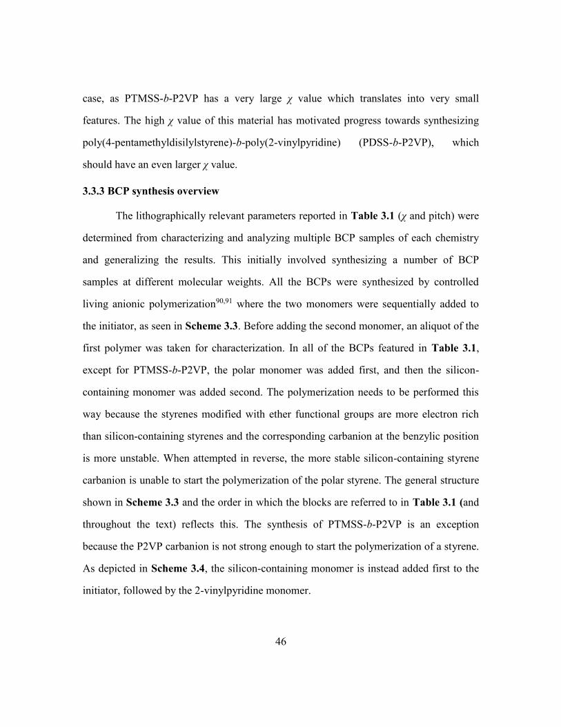
46
case, as PTMSS-b-P2VP has a very large χ value which translates into very small
features. The high χ value of this material has motivated progress towards synthesizing
poly(4-pentamethyldisilylstyrene)-b-poly(2-vinylpyridine) (PDSS-b-P2VP), which
should have an even larger χ value.
3.3.3 BCP synthesis overview
The lithographically relevant parameters reported in Table 3.1 (χ and pitch) were
determined from characterizing and analyzing multiple BCP samples of each chemistry
and generalizing the results. This initially involved synthesizing a number of BCP
samples at different molecular weights. All the BCPs were synthesized by controlled
living anionic polymerization90,91 where the two monomers were sequentially added to
the initiator, as seen in Scheme 3.3. Before adding the second monomer, an aliquot of the
first polymer was taken for characterization. In all of the BCPs featured in Table 3.1,
except for PTMSS-b-P2VP, the polar monomer was added first, and then the silicon-
containing monomer was added second. The polymerization needs to be performed this
way because the styrenes modified with ether functional groups are more electron rich
than silicon-containing styrenes and the corresponding carbanion at the benzylic position
is more unstable. When attempted in reverse, the more stable silicon-containing styrene
carbanion is unable to start the polymerization of the polar styrene. The general structure
shown in Scheme 3.3 and the order in which the blocks are referred to in Table 3.1 (and
throughout the text) reflects this. The synthesis of PTMSS-b-P2VP is an exception
because the P2VP carbanion is not strong enough to start the polymerization of a styrene.
As depicted in Scheme 3.4, the silicon-containing monomer is instead added first to the
initiator, followed by the 2-vinylpyridine monomer.
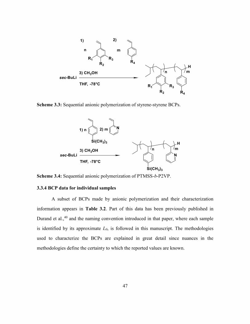
47
Scheme 3.3: Sequential anionic polymerization of styrene-styrene BCPs.
Scheme 3.4: Sequential anionic polymerization of PTMSS-b-P2VP.
3.3.4 BCP data for individual samples
A subset of BCPs made by anionic polymerization and their characterization
information appears in Table 3.2. Part of this data has been previously published in
Durand et al.,40 and the naming convention introduced in that paper, where each sample
is identified by its approximate L0, is followed in this manuscript. The methodologies
used to characterize the BCPs are explained in great detail since nuances in the
methodologies define the certainty to which the reported values are known.

48
Table 3.2: BCP sample characterization summary
a Periodicity from bulk SAXS measurements, annealed at approximately 180 °C. Values in
paranthesis indicate measurements of a disordered sample. b MN (in kg/mol) of aliquot and BCP by MALDI c Dispersity index by SEC. d Degree of polymerization, normalized to 118 Å3
e Dispersity index calculated from MALDI due to sample-specific SEC difficulties

49
3.3.5 BCP pitch
A key value reported in Table 3.2 is the L0 of the BCP sample as measured by
small angle x-ray scattering (SAXS). Within a given class of BCPs, L0 increased
monotonically with increasing BCP molecular weight (MN,BCP) or degree of
polymerization (N), as is expected based on Equation 1.2. When comparing two BCP
samples of different classes but that form approximately the same feature size (ie, PS-b-
PTMSS18 nm and PMOST-b-PDSS18 nm, both forming approximately 18 nm features), the
BCP class with the higher χ-value (PMOST-b-PDSS) forms these features at much
smaller MN,BCP or N. Similarly, when comparing two BCP samples of different classes but
approximately same MN,BCP or N (ie, MN,BCP = 30.7 kg/mol, 29.7 kg/mol and N = 430,
427 for PS-b-PTMSS18 nm, PS-b-PDSS20 nm, respectively), the higher χ-value material
(PS-b-PDSS) forms larger features (~18 vs. 20 nm). The trade-off, of course, is that the
higher χ-value materials stay ordered at lower MN,BCP or N, and can ultimately produce
smaller features. For example, the sample PS-b-PTMSSDis is disordered at MN,BCP = 27.7
kg/mol and the location of its SAXS peak implies the limit of the PS-b-PTMSS class of
materials is more than 17 nm, but the sample PMOST-b-PTMSS14 nm remains ordered at a
much smaller size of MN,BCP = 17.5 kg/mol with a much smaller SAXS peak at
approximately 14 nm.
There exists some discrepancy between the L0 measured by SAXS and the L0
observed in thin films. For example, PMOST-b-PTMSS20 nm has a SAXS peak at 19.6
nm, has been measured to be 19 to 21 nm on different instruments by top-down SEM
inspection, and flips island-hole behavior at multiples of 18.7 ± 0.2 nm. These values
span a range of almost 2.5 nm or approximately 12% of the average full pitch. The SAXS
L0 value is extracted from a bulk sample, so it stands to reason this value could be
intrinsically different from the BCP behavior observed in thin films. Discrepancies in

50
SEM measurements could be attributed to differences in the calibration of the
instruments. The island-hole flipping behavior is harder to explain by instrument error
since two different ellipsometers of different brands with different fitting models have
both produces the same measurement. Again, the island-hole flip is a thin film
phenomenon which could deviate substantially from bulk SAXS measurements. Another
caveat is that L0 is temperature-dependent property of the BCP, so different annealing
conditions could contribute to different results. This is anticipated to be the reason for the
slight discrepancy between the L0 values reported by Durand et al.40 and the results
reported here. Data for the temperature dependency of L0 for these ordered silicon-
containing BCPs has not been collected, but from data collected for disordered BCP
samples, the change in L0 across a 60 °C temperature range is estimated to be on the order
of half a nanometer. Also possible to explain the differences between Table 3.2 and
Durand et al. is drift in the SAXS instrument. Throughout the years, the detector and the
optical train on the SAXS instrument have been repaired and/or replaced repeatedly.
Despite calibrating the instrument before each sample run, it is possible that a systematic
error in the tool has emerged that would skew the L0 one way or the other. Because of all
these factors, the uncertainty in reported L0 values have an estimated uncertainty between
5 and 10%, and the reported and discussed L0 is always the value from SAXS. The raw
SAXS profiles are included in Appendix A.
3.3.6 Characterization procedures
The number average molecular weight (MN) of each homopolymer aliquot (MN,Ali)
and of each corresponding BCP (MN,BCP) are reported in Table 3.2 and were determined
by matrix-assisted laser desorption/ionization time-of-flight (MALDI-TOF)
spectrometry. Since MALDI-TOF is a non-destructive mass spectrometry technique, the

51
data collected are the ratio of polymer chain mass to charge (m/z), allowing for the
absolute determination of the molecular weight and molecular weight distribution of a
sample. BCP MN is needed to calculate the degree of polymerization N of the sample,
which is used in calculating χ. MN,Ali is reported to guide future synthesis of materials.
Calculating MN by MALDI is preferable to calculating it by size exclusion
chromatography (SEC) since SEC requires the calculation of the change in refractive
index of the solution (dn/dc) for each sample to properly determine the exact MN. This is
difficult because the present sample set includes polymers of many different chemistries,
which would require repeated determination of dn/dc, and in addition, some of the
sample MN’s are in the regime where dn/dc is not a constant, so dn/dc would need to be
calculated individually for each sample. MALDI does not face these drawbacks, and in
fact performs better as the MN decreases. The raw MALDI spectrum are included in
Appendix A.
The dispersity index (Đ) reported in Table 3.2 was, in contrast, determined by
SEC, and is reported to quantify the quality of each BCP samples. Products produced by
unintended side-reactions during the anionic polymerization appear as peaks in SEC.
These side-reactions would potentially not appear in a MALDI spectrum, for example,
necessitating the use of SEC to characterize the MN distribution. The Đ-values in Table
3.2 are all below 1.10, indicating that the homopolymers and the BCPs were polymerized
in a living manner without terminating side-reactions. This is partially due to deliberately
only choosing monomers that undergo anionic polymerization without side-reactions, and
also due to rigorously following the air-free/water-free procedures to ensure no events
occurred during polymerization to generate a large amount of dead homopolymer. The
PTMSS-b-P2VP samples in Table 3.2 have Đ > 1.10, but this is most likely due to the
SEC’s inability to properly measure such small samples (MN,ALI < 4 kg/mol), which no

52
doubt fall outside the instrument’s range. Inspection of the raw SEC traces (all of which
are included in Appendix A) corroborates that these homopolymer peaks have narrow
dispersity and no indication of poor synthesis control. In addition, the Đ of the two
smallest PMVBD-b-PDSS samples are instead reported from MALDI due to difficulties
in obtaining these SEC traces.
From the MN,BCP values, N was calculated, and this was used to calculate χN for
each sample. The reported N-value is normalized to 118 Å3, a common but arbitrary
reference volume for BCPs.92 Normalization of N allows direct comparisons to be made
between different BCPs. As previously discussed, χN is a measure of the segregation
strength of the BCPs. The BCPs reported here bridge the weak segregation limit and the
strong segregation limit, so it was necessary to calculate χN to quantify how close a BCP
sample was to its disordered state.
3.3.7 Calculating χ by dynamic mechanical spectroscopy
In addition to determining N of the BCP, the last piece required to calculate the χ-
values is the order-disorder transition temperature (TODT) of individual samples. Since χ is
a function of temperature as shown by Equation 3.1:
𝜒 =𝑎
𝑇+ 𝑏 (3.1)
where T is absolute temperature and a and b are constants, there exists a temperature at
which a given BCP sample goes from ordered to disordered (χN > 10.5 to χN < 10.5).
Such a transition be can monitored by dynamic mechanical spectroscopy (DMS). Upon
heating a bulk BCP sample, the transition from order to disorder is accompanied by a
precipitous drop in the elastic modulus (G’).93 However, not every BCP sample will have
a measurable TODT. For a TODT to be measurable, the value needs to be above the glass

53
transition temperature (Tg) of the BCP sample but below the degradation temperature of
the sample. For example, it was shown that a relatively high χ BCP, poly(4-tert-
butylstyrene)-b-poly(methyl methacrylate), with a relatively high dependency of χ on
temperature (a = 41 K from Equation 3.1) had accessible ODTs only for samples
between approximately 17-31 kg/mol in weight.54 In practice, this range can be even
smaller depending on the specific BCP’s properties, as well as how far away from the
degradation point one wishes to operate. Using a rheometer, the TODT of a number of the
samples in Table 3.2 were discovered and are reported in Table 3.3.
Table 3.3: Summary of ODT data used to determine χ at 180 °C
a Temperature of order-disorder transition measured by rheology b Uncertainty in the temperature, degree of polymerization, and temperature coefficient c Calculated χ value at 180 °C d Propagated uncertainty in χ value
As seen in Figure 3.2, even below the nominal degradation temperature, visible
discoloration occurs due to oxidative damage in the benzodioxole polymers (PVBD and

54
PMVBD) when they are heated to find the OTD. Compared to the corresponding ether,
poly(3,4,5-trimethoxystyrene), the benzodioxole moieties show significantly greater
oxidative damage, even at a modest temperature of 160 °C. After being raised above 250
°C, the samples are clearly an amber color. It is anticipated that the benzodioxole
transforms into a catechol, as has been reported by other researchers.94 Ironically, this is
anticipated to actually raise χ in our favor, as the phenolic moieties on the catechol are
actually more hydrophilic than the parent benzodioxole. Of course, this means that the χ
determined by this method is not the true χ of the parent molecule, but is the effective χ of
the partially modified benzodioxole BCP. Since the typical thin film annealing conditions
also subject the BCP to > 160 °C temperatures in air (presumably allowing the same kind
of oxidation to occur) no attempts were made to differentiate between the actual χ and the
effective χ.
Figure 3.2: Polymers showing signs of oxidation damage during and after rheology
experiments.

55
Of the seven classes of BCPs introduced in Table 3.1, only one class, PMOST-b-
PDSS, did not have a sample with an accessible TODT in Table 3.3. A value for a
hypothetical TODT was estimated for the sample PMOST-b-PDSSDis. An upper value was
concretely established by the DMS experiment (the sample was disordered even as low as
145 °C). A lower bound of approximately 85 °C was determined from comparing it to
other materials (the χ of PMOST-b-PDSS would have to be lower than that of PMOST-b-
PTMSS for this sample’s TODT to be less than 85 °C, which is unlikely due to scaling
arguments of L0 vs. χ and previous trends associated with changing PTMSS to PDSS).
This uncertainty in TODT for PMOST-b-PDSSDis is reflected in Table 3.3, whereas the
uncertainty in TODT is lower for the other samples and is attributed to the discrepancy
between the thermocouple’s location in the rheometer and the polymer sample’s location.
Table 3.3 again reports the N of each sample, as well as calculated uncertainty in N
arising from uncertainty in MN,BCP (depending on how one analyzed the MALDI
spectrum, the calculated MN,BCP could differ by approximately 3%).
With just N, one could use the mean field theory result χN = 10.5 to calculate the
χ of the BCPs, but this value would only be true at the TODT. Since the measured TODT’s
span a range of almost 100 °C, these χ-values could not be used to make accurate
comparisons between the BCP materials, and instead necessitates the calculation of χ at
the same temperature using Equation 3.1. To use this equation, the constants a and b
need to be fitted, however, only three of the seven BCP classes had samples with multiple
TODT’s, precluding the direct determination of a and b for each class. Since b is a constant
for a given BCP, Equation 3.1 can be combined with itself to write Equation 3.2,
removing the need to calculate b explicitly:

56
𝜒1 −𝑎
𝑇1= 𝜒2 −
𝑎
𝑇2 (3.2)
A value for a is still needed to perform the calculation. Again, this value can be
calculated from Equation 3.1 for PS-b-PTMSS, PVBD-b-PDSS, and PTMSS-b-P2VP
since multiple samples with these chemistries had measurable TODT’s, and these are the
values reported in Table 3.3. To estimate a for the other four BCP chemistries, inferences
had to be made from the samples that did not have measurable TODT’s. For example,
although PMVBD-b-PDSS10.5 nm had a TODT at 247 °C, PMVBD-b-PDSSDis had no
measurable TODT, which placed an upper limit on a for the PMVBD-b-PDSS BCP class.
In addition, a has been experimentally determined for a number of different BCPs in the
literature,86 supplying guidance for reasonable values for a. Because of the lack of solid
evidence for most of these materials, the uncertainty in a has been over-estimated in
Table 3.3, sometimes being stated as 2/3 of the actual value. It was discovered that the χ
dependency on a does not greatly affect the uncertainty over the temperature range 160
°C < T < 260 °C, due to the Arrhenius-like relationship between χ and temperature.
Solving Equation 3.2 for χ2 and replacing χ1 and T1 with the more precise χODT
and TODT yields Equation 3.3:
𝜒2 = 𝜒𝑂𝐷𝑇 + 𝑎 (1
𝑇2−
1
𝑇𝑂𝐷𝑇) (3.3)
Again, T2 is set equal to 180 °C to be in line with the SAXS data and because this
temperature is approximately the temperature at which thin film annealing is performed,
making it a relevant temperature at which to compare χ. χODT is again from χN = 10.5 at
the ODT. The calculated values of χ2 are listed in Table 3.3 for each individual sample
with a TODT (and PDSS-b-PMOSTDis). For the BCP chemistries with multiple samples
that have a TODT, it is satisfying to see that the calculated χ-values are within the margin

57
of error. In Table 3.1, the average of the two χ-values is reported for the BCPs with more
than one measurable TODT, and the reported uncertainty is the larger of the two in Table
3.3. For the other four BCP chemistries, the reported χ-value and uncertainty at 180 °C in
Table 3.1 is the result from the one sample in Table 3.3.
To calculate the final uncertainty in χ, the variance formula was used with
Equation 3.3 to yield Equation 3.4:
Δχ = √(𝜕χ
𝜕𝑎∙ Δ𝑎)
2
+ (𝜕χ
𝜕𝑇𝑂𝐷𝑇∙ Δ𝑇𝑂𝐷𝑇)
2
+ (𝜕χ
𝜕𝑁∙ Δ𝑁)
2
(3.4)
where each partial derivative is calculated as follows:
𝜕χ
𝜕𝑎= (
1
𝑇2−
1
𝑇𝑂𝐷𝑇) (3.5)
𝜕χ
𝜕𝑇𝑂𝐷𝑇= −
𝑎
𝑇𝑂𝐷𝑇2 (3.6)
𝜕χ
𝜕𝑁= −
10.5
𝑁2 (3.7)
The variance in a contributed most significantly to Δχ for PMOST-b-PDSS and PMVBD-
b-PDSS. These two polymers had the largest initial Δa, and χ had to be extrapolated 65
and 67 ° to 180 °C, respectively, among the largest extrapolation required. Both PVBD-
b-PDSS samples also had larger-than-average a variance contributions, also because of
the large temperature range of extrapolation. The variance contribution of TODT was only
very significant for PMOST-b-PDSS, again because the actual TODT was never measured
for any of these samples and had to be inferred. The variance due to N was generally the

58
lowest contribution to Δχ and increased as N decreased for the higher-χ BCPs, due to
scaling as 1/N2.
The preceding analysis is important because it allows for direct comparison of
BCP chemistries. Specifically, it shows that χ was increased substantially by polymer
modification, a very satisfying result in terms of “engineering” materials for lithographic
applications. In addition, χ is a parameter in Equation 1.2, needed to calculate L0 at a
given segregation strength. Three materials, PVBD-b-PDSS, PTMSS-b-P2VP, and
PMVBD-b-PDSS, emerged as very high-χ materials whose full pitch can be as small as
10 nm. From the data described above, more information about the full potential of these
materials can be gleaned.
3.3.8: Extrapolating scaling trends
The actual pitch a BCP can make is perhaps the most significant parameter in
lithographic applications. Although χ is often used as the benchmark to compare different
BCP materials, L0 is not determined solely by χ. Equation 1.2 links L0 to χ and N and is
reprinted here:
𝐿0 = 𝛼𝜒1/6𝑁𝛿 (1.2)
where α contains the statistical monomer length, approximately 1 nm but different for
every BCP chemistry, and δ has been calculated to be 1/2 in the weak segregation regime
and 2/3 in the strong segregation regime.19,22 The BCP materials described here span
these two theoretical extremes, which necessitates the extraction of δ from data. Taking
the logarithm of both sides of Equation 1.2 yields Equation 3.8,
log (𝐿0) = log(𝛼𝜒1/6) + 𝛿log (𝑁) (3.8)
and provides a linear relationship for L0 and N. Equation 3.8, along with the SAXS L0
and N data reported in Table 3.2 and with the χ calculated at 180 °C were used to

59
generate Table 3.4. Of note is that the relationship expressed in Equation 1.2 is perhaps
more accurately represented by the radius of gyration (RG) of the BCP rather than N, but
N is the value more readily determined in glassy polymers.
Table 3.4: Parameters for domain spacing calculations
a Parameters forL0 = α·χ1/6·Nδ extracted from linear regression of log-log plot of N and L0 and the
confidence interval on the values. α has units of nm. b Coefficient of determination for the linear regression of log-log plot of N and L0 c Range of χN values of the samples used to calculate the regression
Table 3.4 reports the calculated values for α and δ, their confidence intervals, the
coefficient of determination for the linear regression, and calculated L0’s at a number of
χN values for each BCP chemistry. Both α and δ vary substantially from sample to
sample, but the confidence interval for these values are very large and it is difficult to
draw meaningful conclusions solely from these values. The confidence intervals for δ

60
capture values reported for other BCPs (0.5 to 0.8)54 despite only fitting 2-4 BCP
samples.
In order to calculate L0 at a number of χN values for Table 3.4, the quantity χN
was defined as a constant:
𝜒𝑁 = 𝐶 (3.9)
Solving Equation 3.9 for N and substituting into Equation 1.2 yields Equation 3.10:
𝐿0 = 𝛼𝜒1/6−𝛿𝐶𝛿 (3.10)
The χN range of the BCP samples used to derive α and δ are included in Table 3.4, which
shows the range over which Equation 3.10 can be trusted to produce accurate values for
L0. Unfortunately, samples of χN > 14 were not available for the three BCPs with the
highest χ-values, and a χN > 16 sample was not available for PS-b-PTMSS, necessitating
that the calculated L0’s at these χN’s be extrapolated. It is anticipated but cannot be
guaranteed that the power-law behavior calculated at lower χN’s will be applicable at
these higher χN’s. The coefficient of determination of the log-log relationship in all cases
is very close to 1., strengthening the argument that the linear fit of the log-log data is a
good fit.
The increments for χN were chosen to represent a range of values that might
represent the lower bound of the segregation force required to make viable BCP
structures for lithography,85,95 but of course, this requires extrapolating far beyond the χN
range of the initial data for PVBD-b-PDSS, PTMSS-b-P2VP, and PMVBD-b-PDSS,
making the calculations at χN = 14 and 16 less meaningful. As seen in Table 3.4, the
confidence intervals for L0 of PTMSS-b-P2VP at χN = 14 and 16 are very large and do
not make significant predictions about the material’s performance.
Importantly, Table 3.4 predicts that the 10 nm features made by these three
highest-χ BCPs are not very highly segregated, even by the standards of the samples in

61
this study. Etch tests are underway with some of these near-10 nm samples to determine
if pattern transfer can be accomplished nonetheless.
Curiosity drove us to see if we could decouple the scaling of the BCPs from their
explicit chemistries, in other words, was there a universal scaling law for BCPs? This
would help guide efforts to make BCP materials that could make 8 nm features and
below. Plotting the calculated pitch of each BCP chemistry against the chemistry’s
calculated χ at constant χN produced a plot with a power law behavior. These data were
then plotted on a log-log plot, as shown in Figure 3.3A and quantified by the following
two empirical equations:
𝐿0 = 𝛽𝜒𝜆 (3.11)
log (𝐿0) = log(𝛽) + 𝜆log (𝜒) (3.12)
where β and λ are empirical constants. For clarity, Figure 3.3A shows only the results for
χN = 10.5 and 14, but χN = 12 and 16 follow the same general trend. In Figure 3.3A, the
points are numbered according to the BCP chemistry to which they belong, with
increasing number corresponding to increasing χ (an explicit listing also appears in the
caption). The BCPs satisfyingly fall on a line until the last three, high-χ BCPs. With these
last three samples, PVBD-b-PDSS and PMVBD-b-PDSS fall slightly below the trendline,
while PTMSS-b-P2VP falls significantly above it. This fact can also be discerned from
the residual plot in Figure 3.3B. Again, points 5 and 7 (PVBD-b-PDSS and PMVBD-b-
PDSS) are below zero, and point 6 (PTMSS-b-P2VP) is above zero. The residuals for the
rest of the data points seem to be randomly distributed with no clear trends.

62
Figure 3.3: (A) Log-log plot of L0 calculated at two different χN values (10.5 and 14)
versus χ at 180 °C. Line is least squares residual fit. (B) Residual plot of the
linear regression through the points in plot (A). Lines are added to guide the
eye. Numbers in both graphs correspond to the BCPs as follows: (1) PS-b-
PTMSS (2) PS-b-PDSS (3) PMOST-b-PTMSS (4) PMOST-b-PDSS (5)
PVBD-b-PDSS (6) PTMSS-b-P2VP (7) PMVBD-b-PDSS.
The values of β and λ were extracted from Equation 3.12 and are summarized in
Table 3.5. Remarkably, the exponent for χ, λ, is approximately constant at -0.44 for this
range of χN values. The prefactor β, however, is a function of χN and increases with
increasing χN. Unfortunately, the calculated uncertainties from Table 3.4 and Equation
3.10 for L0 and χ resulted in even larger uncertainties in β and λ. The power law
relationship between L0 and χ is very sensitive to even small degrees of uncertainty in the
constituent values used in the calculation. Nonetheless, these values were used to
evaluate Equation 3.11 for L0 = 8 and 6 nm to probe approximately what kind of
materials are needed to make features this small. As seen in Table 3.5, the predicted χ-
values ranged from 0.15 to 0.25 depending on χN for 8 nm features, and from 0.29 to

63
0.53 for 6 nm features. These values were then used to calculate the N of the hypothetical
BCP, and approximate MN (the true MN would be dependent on the density of the BCP
blocks). Again, the large uncertainties in β and λ created even larger uncertainties in these
χ-values, in this case to the point of making them near meaningless. The smallest
uncertainties were ± 50% of the calculated χ values, and the largest uncertainties were +
200% and – 80%. Due to this large range of values, the uncertainties were not reported in
Table 3.5.
Table 3.5: Summary of empirical model for predicting scaling limits
a Parameters for L0 = β·χλ extracted from linear regression of log-log plot of L0 and χ at constant
χN.
To decrease the uncertainty in β, λ, and χ at 8 and 6 nm, better values are needed
for χ of the known BCP chemistries and L0 of the individual BCP samples. The largest
contributor to the uncertainty in χ of the known BCP chemistries is the extrapolation of χ
from the TODT to the reference temperature (180 °C). If additional BCP samples were
available that contained measurable TODT’s, and the TODT’s bracketed the reference

64
temperature so that interpolation was used to calculate χ, the uncertainty in χ would
decrease substantially. The uncertainty in L0 is due to the variability of the SAXS
measurements. As discussed previously, the measurements were taken on potentially
unstable equipment over a period of many years, with many variations in the sample
preparation protocol from operator to operator. Uniformly constructing and annealing the
samples, and then taking the measurements all at once on the same equipment in a
consistent manner, would substantially decrease the variability in the output of the SAXS
experiment and the corresponding uncertainty in L0.
With the concerns about the uncertainty of the hypothetical χ-values at 8 and 6 nm
in mind, there are still meaningful inferences to be made from Table 3.5. First, to go
from materials that can make ~10 nm full pitch features (like the ones described in this
manuscript) to materials that can make ~8 nm full pitch features, at the minimum a 50%
increase in χ is required. The structural changes that transformed PS-b-PTMSS into
PMVBD-b-PDSS increased χ almost 400%, but it is not immediately clear if any
additional changes are possible to produce a material with a further incremental increase
in χ (and that is still compatible with the top coat orientation strategy). In addition, to
further increase the resolution from 8 nm to 6 nm, χ needs to double. Again, the route to a
material with such a large χ is not clear. Furthermore, the calculated N and MN of the
hypothetical 6 nm materials indicate BCPs composed of essentially oligomers; it is hard
to imagine that these materials, which are essentially liquid crystals, would follow trends
extrapolated from materials an order of magnitude larger. Deviations from the described
trend, however, could be beneficial and not detrimental. As shown in Figure 3.3A, it
appears PVBD-b-PDSS and especially PMVBD-b-PDSS produce smaller features that
those predicted by the model that describes the behavior of BCPs with lower χ values at
higher N’s. Conversely, the features made by PTMSS-b-P2VP are much larger. These

65
differences in L0 are beyond the error expected from the SAXS measurements and
indicative that a single empirical model that describes all BCP behavior is probably non-
existent.
3.4 CONCLUSIONS
In conclusion, variety of lamellae-forming BCPs were synthesized and
characterized as candidate materials for lithography. The BCPs were alike in that they all
had a styrenic (or nearly styrenic, in the case of P2VP) backbone. Each BCP contained a
silicon-containing block to be used as an etch mask, and was paired with a polar block.
The chemistry of the polar block was the single largest difference from BCP to BCP, and
choosing especially polar blocks created BCPs with high χ-values that ultimately
produced 10 nm and smaller features.
A general model was proposed to correlate L0 and χ, regardless of chemistry, and
was fit by the seven BCP examples introduced in this chapter. At different segregation
strengths, a power law model described the L0 behavior quite well. This model was used
to draw inferences about the kinds of materials needed for 8 and 6 nm pitch feature
production. Unfortunately, the model predicts that substantial increases in χ are needed to
produce features this small. However, the actual BCP data at small L0 seems to deviate
from the predicted trends, with samples making both larger and smaller L0’s than
predicted, which invites optimism about the scaling limits of BCPs.
BCPs described in this Chapter were used in directed self-assembly (DSA)
experiments to make device relevant line-space features. For example, Maher et al. used
PS-b-PTMSS22 nm at IBM to make patterns through a variety of mechanisms.96 Cushen et
al. used PMOST-b-PTMSS20 nm (as well as a 17 nm sample not introduced here) at HGST
for bit-patterned media applications.97 The last two chapters describe the work of the

66
author and coworkers with PMOST-b-PTMSS20 nm and PVBD-b-PDSS10.5 nm at IMEC
and Seagate, respectively.
3.5 EXPERIMENTAL
3.5.1 BCP synthesis
BCPs were synthesized according to the following general procedure. The
monomers were trap-to-trap distilled out of dibutyl-butyl magnesium twice and finally
collected in an empty, flame dried Schlenk flask. A 500 mL glass reactor with 5 threaded
ports was charged with a Teflon-coated magnetic stir bar and the following were attached
to the ports: a thermocouple well, a septum-capped inlet port (attached to a Schlenk line
and a pressure gauge), a 500 mL solvent flask of ~150g THF, and 2 glass blanks. The
reactor was flame dried under high vacuum and purged five times with Ar. The purified
THF was added to the reactor while maintaining a slight 3 psig overpressure. After
cooling to – 78 °C, a solution of sec-butyllithium (1.4 M in cyclohexane, Aldrich) was
added to the reactor through the septum via an air-tight syringe. The first monomer was
then added, also by syringe, and allowed to react for 1 to 3 hours. An aliquot of
approximately 3 mL was taken and injected into degassed methanol, before adding the
second monomer by syringe. The reaction continued to be stirred for 1 to 3 hours and
then terminated by addition of degassed methanol. The THF solution was concentrated
slightly (target: 5 g THF / 1 g polymer) and precipitated into methanol. The isolated
white powder was dried in vacuo.
3.5.2 Characterization
SEC was performed using a Viscotek VE 2001 triple detector gel permeation
chromatograph with an Agilent 1100 Series isopump and autosampler. THF was used as

67
an eluent at 1 mL/min and 23 °C with three I-series mixed bed high-MW columns,
calibrated against PS standards.
MALDI data were collected on an AB SCIEX Voyager-DE PRO MALDI-TOF
using trans-2-[3-(4-tert-butyl-phenyl)-2-methyl-2-propenylidene] malononitrile (DCTB)
as a matrix with silver trifluoroacetate as the counterion. The baseline of the MALDI
spectra was fitted to a quadratic function and subtracted.
SAXS measurements were collected using a Molecular Metrology instrument
equipped with a high brilliance rotating copper anode source (Kα radiation) and a two-
dimensional 120 mm gas filled multiwire detector. The beam was calibrated using silver
behenate with its primary reflection peak set at 5.838 nm. Samples were prepared by
annealing polymer inside of a Viton o-ring in between Kapton tape on a hotplate.
Rheology data were collected on a TA Instruments AR2000EX using a 25 mm
parallel plate operating in strain controlled mode. Each sample was measured at strain =
2% and angular momentum ω = 1 rad/s in the linear viscoelastic regime. Samples were
ramped at 5 °C/min under nitrogen flow while monitoring the storage modulus, the loss
modulus, and the difference between the two (delta).
3.5.3 Regression procedures
Equations 1.2 and 3.11 were fitted by least squares residual linear regression of
the logarithm of both values. Uncertainty in the slope and y-intercept was determined by
the method of maximum/minimum values for the first and last data points.

68
Chapter 4: Directed self-assembly for semiconductor applications
The work in this chapter has been reproduced in part with permission from
Blachut, G.; Sirard, S.M.; Maher, M.J.; Asano, Y.; Someya, Y.; Lane, A.P.; Durand,
W.J.; Bates, C.M.; Dinhobl, A.M.; Gronheid, R.; Hymes, D.; Ellison, C.J.; Willson, C.G.;
“A hybrid chemo-/grapho- epitaxial alignment strategy for defect reduction in sub-10 nm
directed self-assembly of silicon-containing block copolymers.” Chemistry of Materials
2016. DOI:10.1021/acs.chemmater.6b03633. The author performed the majority of the
studies in this manuscript. Parts of the chapter have also been reproduced with permission
from Cushen, J.; Wan, L.; Blachut, G.; Maher, M. J.; Albrecht, T. R.; Ellison, C. J.;
Willson, C. G.; Ruiz, R. “Double-Patterned Sidewall Directed Self-Assembly and Pattern
Transfer of Sub-10 nm PTMSS-b-PMOST.” ACS Appl. Mater. Interfaces 2015, 7, 13476-
13483. The author prepared the BCP samples and provided the BCP characterization data
for this manuscript. Copyright 2015-2016 American Chemical Society.
4.1 BACKGROUND
A number of creative methods to produce long range order in thin films of block
copolymers (BCPs) appear in the literature. Electric fields,98 heterogenous substrates,99
pressure gradients,100 and temperature gradients101 have all been used to order BCPs
along a desired axis. However, to make device-relevant features with BCPs, directed self-
assembly (DSA) techniques are required. DSA is needed to precisely place the BCP
features, especially in relationship to pre-patterned structures on the substrate. A key
practical aspect of DSA is that DSA implementations need to densify or multiply a sparse
initial pre-pattern; simply replicating a pattern 1:1 is insufficient. In addition to
“frequency multiplication” or “pattern interpolation” to increase the final feature density,

69
DSA can rectify errors in the initial lithography.102,103 This phenomenon may become
more significant as the feature size decreases.
DSA techniques have been broadly categorized as grapho-epitaxy104,105 or chemo-
epitaxy,102,106,107 depending on how the pre-pattern is constructed. In grapho-epitaxy,
topography on the substrate serves as the registration point for BCP domains. In chemo-
epitaxy, chemical contrast, often thought of in terms of surface energy differences or
gradients, serves as the anchoring force for different components of the BCP. Grapho-
epitaxy is often easier to implement since there are an assortment of ways to create the
requisite topography,108–110 and the pre-pattern’s pitch and dimensions can be hundreds of
nanometers. However, grapho-epitaxy often necessitates the sacrifice of usable areal
space due to the topography, making it less desirable for some high density applications.
Chemo-epitaxy, in comparison, typically sacrifices no areal space, and the near-planar
under-layer adds minimal complexity to the film stack, helping to facilitate subsequent
pattern transfer. Unfortunately, chemo-epitaxy is often much harder to implement. The
surface tension of the patterned regions must be precisely tuned for a BCP system,57,59
and often custom materials are required for a given BCP chemistry. The initial
lithography for chemo-epitaxy is more demanding as well: the pre-pattern pitch is often
no more than 4 or 5 times the BCP natural periodicity (L0), and the actual feature size
might be a fraction of L0. It should be noted that most DSA schemes actually implement
aspects of both grapho- and chemo-epitaxy: the surface tension of topographic features is
a significant parameter in determining the orientation of BCP domains,105 and “planar”
chemo-epitaxy often contains height differences between the different chemical
regions.111 In addition, recently “hybrid” epitaxy processes have emerged, where
chemical pre-patterns and topography are deliberately used in conjunction for
DSA.97,112,113 The difference between hybrid processes and most grapho-epitaxy

70
processes is that the topography in hybrid processes is shallower than the BCP film
thickness, as to not sacrifice any usable areal space. Hybrid processes often have the
advantage that their defectivity is lower than chemo-epitaxy processes.
Progress has been made in implementing a chemo-epitaxy process for PS-b-
PMMA on 300 mm wafer processing equipment with state-of-the-art 193 nm immersion
lithography (193i) at IMEC114–116 and other laboratories.117 The process at IMEC is based
on a modified LiNe process,57,59 depicted in Figure 4.1. To compatibilize the laboratory-
scale LiNe process (which used electron beam lithography) with 193i, a film stack was
developed to allow high resolution photolithography. Specifically, a 13 nm thick silicon
nitride layer is needed, in conjunction with the 7 to 8 nm thick polymer underlayer, to
form a suitable anti-reflective coating for 193i.114 The LiNe flow employs a trim etch to
simultaneously reduce the dimension of the lithographically-defined resist features
(“trim”) and transfer the resist feature pattern into the underlying polymer layer. A
second polymer is then “backfilled” into the region exposed by the trim etch, producing a
surface with alternating surface energy stripes of unequal width. The surface tension of
these two polymeric regions needs to be tuned precisely to the BCP chemistry and often
requires refinement for a new BCP formulation. To be “drop-in” compatible with 300
mm wafer processing, the LiNe process utilizes only spin-coating to deposit polymers,
and only baking (thermal annealing) for the various annealing steps.

71
Figure 4.1: Fabrication of chemical pre-patterns used for the directed self-assembly of
PS-b-PMMA with frequency multiplication. Reproduced with permission
from Liu et al. “Chemical Patterns for Directed Self-Assembly of Lamellae-
Forming Block Copolymers with Density Multiplication of Features.”
Macromolecules 2013, 46, 1415–1424.
This chapter describes the implementation of a 193i-compatible DSA process for
silicon-containing BCPs at IMEC. Modifying the existing chemo-epitaxy process at
IMEC to be suitable for silicon-containing BCPs was possible but required the
introduction of new polymeric materials with surface energies relevant for the BCP.
Beyond the introduction of new materials, the processing steps used to fabricate pre-
patterns and form DSA were largely unchanged, demonstrating the viability of silicon-
containing BCPs as smaller pitch replacements for PS-b-PMMA. First, the materials and
processes are introduced. In addition to a traditional chemo-epitaxy process, a hybrid
process utilizing shallow topography was implemented to investigate the advantages of
such a scheme. The DSA results are presented in summary and an in-depth study of the
mechanism of DSA in the hybrid process follows. After that, various DSA process
parameters are quantitatively analyzed. The hope is that an exhaustive description of the
procedures and parameters creates a roadmap for implementation of future materials.

72
4.2 MATERIAL DESIGN AND CHARACTERIZATION
4.2.1 Overview of materials
A silicon-containing BCP, polymer brushes, guide stripe material, and a top coat
were designed, synthesized, and analyzed at The University of Texas specifically for this
collaboration. The chemistry of the materials are depicted in Figure 4.2. Nissan
Chemical graciously demetallized the polymers through an ion-exchange process,
formulated the polymers for spin-coating, and shipped them to IMEC.

73
Figure 4.2: Polymers introduced into IMEC: cross-linkable poly(4-methoxystyrene)
(XPMOST), 4 polymer “brushes” of hydroxyl-terminated polystyrene-r-
poly(4-tert-butylstyrene), the silicon-containing BCP poly(4-
methoxystyrene)-b-poly(4-trimethylsilylstyrene), and the polarity switching
top coat.
The BCP chemistry and periodicity (L0) were chosen in tandem for lithographic
performance. A full pitch of approximately 20 nm was selected as an initial target for the
experiment; this value is 10% smaller than the ~22 nm practical limit of poly(styrene)-b-
poly(methyl methacrylate) (PS-b-PMMA)33 and 30% smaller than IMEC’s ~28 nm
process of record (POR) PS-b-PMMA,116 demonstrating the ability of silicon-containing
BCPs to form lithographically viable features smaller than PS-b-PMMA. Importantly, 20
nm is 1/4 of 80 nm, so a hypothetical 20 nm BCP multiplies the approximate resolution
limit of 193i by a factor of four.12 While frequency multiplication factors larger than 4x
are possible, sparser pre-patterns generally lead to larger defectivity as the driving force
for alignment decreases. The approximate resolution limit for the simplest silicon-
containing BCP we had success orienting, poly(styrene)-b-poly(4-trimethylsilylstyrene)
(PS-b-PTMSS), is 20 nm, but diffuse interfaces in BCPs near the order-disorder transition
(ODT) complicate pattern transfer and made this sample unattractive for a 20 nm
lithographic material.40,85,95 Poly(4-methoxystyrene)-b-poly(4-trimethylsilylstyrene)
(PMOST-b-PTMSS) emerged as an alternative BCP chemistry. The BCP monomers were
readily available, and the synthesis of PMOST-b-PTMSS could be performed in a living
and controlled manner by anionic polymerization. The resolution limit of PMOST-b-

74
PTMSS was determined to be approximately 14 nm, so a sample large enough to form 20
nm features was well within the ordered regime. Most importantly, PMOST-b-PTMSS
responded to the confined island-hole test, enabling the identification of neutral top coats
to generate perpendicular features.39 This BCP, introduced as PMOST-b-PTMSS20 nm in
Chapter 3, was made on a 50 g scale to ensure sufficient material for multiple
applications, and in fact this material was used in bit patterned media studies at Hitachi
Global Storage Technologies97 and Seagate Technology.
4.2.2 Surface treatments
Polymer brushes for surface modification for DSA were also prepared on large
scale. As mentioned in Chapter 2, random copolymers of polystyrene (PS) and poly(4-
tert-butylstyrene) (PtBuS) were made as PS wets the poly(4-methoxystyrene) (PMOST)
BCP block and PtBuS wets the poly(4-trimethylsilylstyrene) (PTMSS) block, so each
BCP component’s affinity for the brush surface could be modified by changing the
composition of the brush. Table 4.1 lists the polymer brushes introduced into IMEC,
their composition, and their wetting preference for the BCP. Island-hole118 tests were
performed to determine the wetting preference. Brushes were grafted onto blank wafers,
and BCP films of various thicknesses were coated. It was important to perform this test at
IMEC since the demetallization of the polymers by Nissan Chemical had the potential to
change the brush properties. Figure 4.3 shows the results of the island-hole test which
was used to determine wetting behavior and populate Table 4.1. Two of the tested
brushes showed “hole” features which indicate symmetric wetting when 1.5 L0 < BCP
film thickness < 2.0 L0, and the third showed neutral wetting behavior with a flip from
islands to holes within the same BCP film thickness range. (Interestingly, the data show
that the affinity of PTMSS for PtBuSty is higher than the affinity of PMOST for PS,

75
since the sample that contains the most PS, BB-85, is only neutral for the BCP, all of the
other brushes are preferential for PTMSS, and none of the samples are PMOST
preferential.) Fortunately, from these existing samples a brush composition was suitable
for DSA (discussed further on in the chapter).
Table 4.1: Polymer brushes available at IMEC
Sample Composition (mol % PS)1 Wetting preference
BB-27 27 PTMSS-wetting2
BB-50 50 PTMSS-wetting
BB-68 68 PTMSS-wetting
BB-85 85 neutral 1 as determined by 1H NMR 2 this result is inferred from the results of the other tests

76
Figure 4.3: Island-hole data of PMOST-b-PTMSS performed at IMEC on polymer
brushes. B-50 and BB-68 show holes, which implies symmetric (PTMSS)
wetting of the two surfaces. BB-85 shows islands and holes at the two
thicknesses, implying neutral “half” features are present.
A top coat consisting of maleic anhydride alternating with styrene and 3,5-di-tert-
butylstyrene, described previously in Chapter 2, was synthesized for PMOST-b-PTMSS.
Although the top coat neutrality was confirmed at the UT, it was unclear if the ion
exchange process for demetallization would leave the polymer, and its surface energy,
unchanged. Confined island-hole tests,39 where the top coat was applied on top of the
BCP, were performed at IMEC, and are shown in Figure 4.4. As the BCP film thickness
increased from 1.6 to 1.9 L0, the topography changed from dark spots which correspond
to islands, to mottled dark regions, to white spots. Just like the island-hole flip observed

77
for BB-85 in Figure 4.3, this island-hole flip implies that, despite the additional
processing, the top coat remained neutral for the BCP.
Figure 4.4: “Confined” island-hole test of the top coat. The progression from island to
spinodal islands to holes in this BCP film thickness range suggests the
neutrality of the top coat. Underneath the BCP is a PMOST-preferential PS
under-layer.
The last material introduced to IMEC from UT for DSA was a cross-linkable mat
of poly(4-methoxystyrene) (XPMOST). As will be explained shortly, this polymer was
used to form the guide stripes that anchors the BCP in DSA. The performance of this
material in DSA was compared directly to commercial cross-linkable poly(styrene)
(XPS) installed at IMEC for the DSA of PS-b-PMMA. Although the polar component of
the BCP, PMOST, wets both XPS and XPMOST, it was anticipated that the chemical
similarity between XPMOST and PMOST would increase the quality of DSA compared
to the XPS. As an IMEC rule forbade the deposition by hand of any material that enters
the 193i scanner, the XPMOST had to be coated by a track from a small volume dispense
unit (SVDU). This greatly reduced the number of experiments possible with XPMOST,
so a majority of the data was collected on the readily available XPS.

78
4.3 TYPICAL PROCESS TO CREATE DSA WAFERS
Two related processes were used to create the pre-patterns for DSA, and their
relative performance was compared. A relatively standard chemo-epitaxy process,
mimicking IMEC’s establish LiNe process, was created for the silicon-containing BCP,
as was a so-called hybrid process, combining chemical guiding surfaces with topography.
Compared to pure grapho-epitaxy, the topography of a hybrid process is kept shallow to
avoid sacrificing usable areal space. Figure 4.5A shows the process used to make the
hybrid pre-patterns. XPMOST was first spin-coated at 19 nm and cross-linked by thermal
annealing. This cross-linked mat was then coated with a positive-tone resist, exposed
with a commercial 193i scanner, and the resist was developed. The wafer was then
reactive ion etched to shrink the width of the resist (“trim” step) and to remove the
XPMOST mat in the regions not covered by the resist to expose the underlying substrate
(“breakthrough” step). Stripping the resist yielded thin lines of mat that later became the
guide stripes. The polymer brush was then applied by spin-coating and grafted by a
thermal anneal to modify the surface exposed during the breakthrough etch. The final
grafting thickness of the brush was only approximately 7-8 nm, far less than the height of
the guide stripe. The height difference between the brush region and the top of the guide
stripe formed the topography in the system. Excess, ungrafted brush was then stripped
with organic solvent to yield the hybrid pre-pattern. To instead make the chemo-epitaxy
pre-pattern, the mat material, in this case either XPMOST or XPS, was coated at only
approximately 8 nm (versus 19 nm) to produce an essentially flat pre-pattern after
processing, as depicted in Figure 4.5B. Beyond the changes in guide stripe coating
thickness and chemistry, the subsequent steps of cross-linking, patterning, etching, and
depositing brush in the chemo-epitaxial process are otherwise identical to the hybrid
process. For both processes, the DSA film stack was completed by spin-coating the BCP

79
on the pre-pattern, and then the top coat directly on top of the BCP. The wafer was then
heated to anneal the BCP, and then etched a second time to remove the top coat and the
sacrificial PMOST block for imaging. The resulting features were observed chiefly by
automated critical-dimension SEM (CD-SEM).
Figure 4.5: (A) Schematic of the hybrid process used to create the chemical pre-pattern
with shallow topography. (B) Depiction of the corresponding pre-pattern
surface produced by the chemo-epitaxy process.
One oversimplification shown in Figure 4.5 that ends up affecting the DSA
significantly is the incorrect depiction of the guide stripe as having edges normal to the
substrate. In reality, due to the different etch rates between the acrylic photoresist and the
styrenic guide stripe and the imperfect anisotropy of the plasma etch, the guide stripes
have a slanted sidewall. As seen in Figure 4.6, the angle of the sidewall is relatively
shallow, approximately 45 to 60° from the substrate. Since the sidewall was directly

80
exposed to the plasma, it became oxidized and resulted in a very polar surface, which was
anticipated to significantly affect the DSA.
Figure 4.6: Cross-section STEM micrograph of the 19 nm tall guide stripes after etch
and resist strip but before depositing the brush or the BCP. The chromium
capping layer was added to protect the features during cross-sectioning and
to prevent charging during imaging.
4.4 QUALITATIVE COMPARISON OF THE TWO DSA PROCESSES
The DSA of PMOST-b-PTMSS was accomplished via both processes, but the
hybrid process produced higher quality DSA than the chemo-epitaxy process using either
guide stripe chemistry. The three micrographs in Figure 4.7 show the best DSA achieved
by each process, after each process was optimized for pre-pattern pitch, guide stripe
width, brush composition, and BCP film thickness (discussion of the optimization of the
process parameters appears later). As shown in Figure 4.7C, the hybrid process produced
DSA with far fewer defects than either the chemo-epitaxy process made with XPS
(Figure 4.7A) or XPMOST (Figure 4.7B). Unfortunately, the defectivity achieved with
the hybrid process on this initial DSA attempt was still much higher than IMEC’s 28 nm
PS-b-PMMA process,116 and determining the contributors of defectivity is an ongoing
area of research. Still, the ability of the hybrid process to produce better DSA than the
similar chemo-epitaxy process warranted further investigation.

81
Figure 4.7: Representative micrographs of DSA under best conditions using (A) chemo-
epitaxy process with XPS guide stripe (B) chemo-epitaxy process with
XPMOST guide stripe (C) hybrid process with 19 nm tall XPMOST guide
stripe. Scale bar is valid for all images.
Cross-sectional STEM with electron energy loss spectroscopy (EELS) was used
to study the BCP orientation on the topography in the hybrid process. Regardless of the
features observed in top-down SEM, BCPs can adopt complex and non-uniform
morphologies in thin films that may render them useless or at least sub-optimal for
pattern transfer.59 Multiple guide stripe widths were analyzed to probe the influence of
this pre-pattern characteristic on the resulting through-film BCP structures. Figure 4.8
shows STEM EELS cross-sections of the pre-pattern and BCP film stack at three guide
stripe widths. Below each STEM image is a corresponding illustration of the proposed
chain conformation that maintains the pattern fidelity discernable from the EELS images,
offering insight into the key interactions that govern DSA. The green or blue vertical

82
segments in each EELS image map silicon and oxygen, respectively, and correspond to
the PTMSS block (image acquisition differences caused oxygen to be measured over
silicon in Figure 4.8C, but the qualitative result remains the same). The color magenta
maps carbon and corresponds to several different carbonaceous regions in the film: the
vertical magenta domains between the green or blue domains correspond to the PMOST
block, the magenta horizontal stripe on top of the BCP domains is the top coat, the
thinner magenta horizontal line under the BCP corresponds to the brush layer, and the
magenta trapezoid corresponds to the guide stripe. The silicon substrate (green) and the
metal oxide capping layer used for sample preparation (blue) are also seen at the very
bottom and top of the images, respectively. A key difference immediately discernable
from the STEMs is that each guide stripe pins a different number of BCP domains,
demonstrating three different DSA regimes. Going from Figure 4.8A to Figure 4.8C, the
guide strip width increase from 13 to 18 to 28 nm (circa 0.5 to 1.0 to 1.5 L0), which
corresponds roughly to one, two, and three BCP domain situated on top of the guide
stripe, respectively, which is also depicted in the illustrations.

83
Figure 4.8: Summary of the cross-sectional STEM EELS study of BCP on tall guide
stripes in the hybrid flow. Guide stripe width (measured by CD-SEM) (A)
~0.5 L0 (B) ~1.0 L0 (C) 1.5 L0. (Top) STEM EELS mappings of cross-
sectioned DSA film stacks. The legend in the top right describes the
elemental mapping color scheme for all three EELS images. Scale bar is
valid for every image. (Bottom) Schematic of the proposed BCP domain
orientation on guide stripes corresponding to difference quantizations of the
BCPs natural periodicity, along with depictions of the anticipated polymer
chain configuration. As shown in the legend, blue corresponds to PMOST
and red to PTMSS.
Importantly, the STEM EELS micrographs show that the BCP domains travel
vertically through the film without adopting complex 3D morphologies. However, the
tapered, wedge-shaped PTMSS domains in Figures 4.8A and 4.8C and the short PTMSS
domains sitting on top of the guide stripes in Figures 4.8B and 4.8C are both sub-optimal
features. Since the PTMSS domains become the hard mask for pattern transfer, any
degree of non-uniformity in these domains impedes this process. The wedge-shaped
PTMSS domains are a result of the domains ordering over the angled sidewall of the
guide stripe. The XPMOST guide stripe draws the PMOST block to the top of the guide
stripe, placing a PMOST to PTMSS intramolecular interface at the guide stripe edge and
84
the PTMSS domain directly over the sloped sidewall. Hypothetically, modifying the DSA
scheme by changing the guide stripe to be PTMSS preferential places a PMOST block on
either sidewall and avoids PTMSS domain distortion. Wedge-shaped domains or other
distortions are tolerable for PMOST since PMOST is the sacrificial block. The other non-
uniformity in the PTMSS domains, the short PTMSS domains on top of the guide stripes
in Figures 4.8B and 4.8C, are not readily fixed. The height difference between PTMSS
domains on the guide stripes and over the backfill brush region is an inescapable
consequence of using shallow topography. While height non-uniformity complicates
subsequent pattern transfer, the uniform structures present in the top half of the film offer
a potential route for isolating viable mask features.
Wedge-shaped PTMSS domains are absent in Figure 4.8B which indicates a
fundamental difference in the conformation of the BCP in this scenario. The immediately
discernable difference is that the intermolecular boundary of two PMOST blocks- and not
the intramolecular block-block interface- is now situated at the edge of the guide stripe.
As a consequence, at the center of the guide stripe sits a full domain of PTMSS, flanked
by half-domains of PMOST on either side. At first glance, the opposite situation, where
PMOST is the component in the center of the guide stripe, flanked by two PTMSS
domains, is equally valid from an enthalpic standpoint, since in both cases a total of one
domain of PTMSS and one domain of PMOST sit on top of the guide stripe. Ostensibly,
the guide stripe sidewall, oxidized during the trim etch, is polar wetting and produces the
key pinning force to anchor the polar PMOST block and induces the BCP conformation
seen. The net effect is that since the PTMSS domains are not ordered above the sidewalls,
no wedge-shaped domains are formed. On further inspection, it appears the PTMSS
domain sitting on top of the guide stripe potentially has curvature at its base, which could
be attributed to a PMOST wetting layer forming underneath the block to minimize

85
unfavorable enthalpic interactions. To minimize sub-optimal wetting situations, the guide
stripe should be made perfectly neutral for the BCP in the case of 1 L0 pre-patterns. Since
one full domain of PMOST and PTMSS sit on top of the guide stripe in this situation, a
neutral guide stripe’s interfacial contribution to the overall free energy of the system
would be lower, potentially improving the quality of DSA.
Despite the location of the PTMSS domains directly over the sidewall regions
when guide stripe width = 0.5 or 1.5 L0, it is anticipated that the sidewalls also pin the
PMOST block in this situation due to the unfavorable enthalpic interactions of the
oxidized sidewall with the hydrophobic PTMSS block. To accomplish this, the PMOST
domains must “spill-over” the guide stripe, as illustrated in Figures 4.8A and 4.8C. This
proposed topology further exacerbates the sub-optimal wedge shape of the PTMSS
domains. Unfortunately, due to the chemical similarities between the guide stripe and the
PMOST, it is not possible to tell with certainty if a layer of PMOST interfaces with the
sidewall. Efforts are underway to incorporate nitrogen into the guide stripe to serve as an
atomic label in STEM EELS to determine the identity of the BCP component interfacing
with the sidewall.
The preceding analysis of the hybrid process implicates the sidewall as having a
large role in the DSA. From tests done on blanket films, it was shown that the hydroxyl-
terminated brushes do not graft to oxidized XPMOST (or XPS) at the conditions used to
graft them to the inorganic substrate, so the polarity of the sidewall is not significantly
decreased before the BCP is applied. Although polymers oxidized by plasma have been
shown to rearrange to hide polar functional groups from the surface,119 the confined
volume of the guide stripe and its cross-linked nature probably prevents a large degree of
rearrangement from occurring. The BCP is forced to interface with this very polar
surface, which changes the nature of the DSA.

86
4.5 DOCUMENTATION AND CONSEQUENCES OF THE SIDEWALL IN DSA
Since nearly all processes used to make pre-patterns for DSA involve patterning
and plasma etching a surface modification layer covered by resist, it is likely that many
processes already rely on or exploit a polar sidewall as an anchoring surface. A
discussion of some of the most significant contributions to this idea follows, and
concludes with a proposal for a novel way to perform DSA.
One of the first documented instances where an oxidized region of film served as
an anchoring surface for DSA was in work done by Yang et al.107 Plasma etching was not
used to oxidize the surfaces, rather, self-assembled monolayers of
octadecyltrichlorosilane were patterned by interference extreme ultraviolet lithography
(EUVL). The exposed regions became very hydrophilic, while the unexposed regions
remained hydrophobic.44 PS-b-PMMA was then deposited on top of the surface, and after
annealing, the BCP domains aligned themselves to the stripes of alternating surface
energy. Although in this example plasma etching was not used to create oxidized
surfaces, it does demonstrate the potential of a surface modified by oxidation to function
as a pinning line.
Work done by collaborators at HGST explicitly implicates the role of the oxidized
sidewall in DSA. Cushen et al.97 report defect-free DSA of PMOST-b-PTMSS over a
large area using solely XPS for the guide stripe and PS for the backfill brush, subject to
the constraints of shallow topography (brush height << guide stripe height), relatively
dense pre-patterns, and 1 L0 guide stripe width, much like the situation depicted in Figure
4.8B. The authors’ interpretation was that the sidewalls of the guide stripe, oxidized
during etching, provided the chemical contrast for DSA (since the chemically similar
guide stripe and brush imparted no chemical contrast), as seen in Figure 4.9. However,
the DSA was also highly dependent on the topography of the system, which strongly

87
confined the BCP chains and promoted the desired alignment. Even slight deviations
from this confining geometry resulted in no DSA.
Figure 4.9: Orientation of BCP chains in the process flow, depicting the oxidized
sidewalls as guiding interfaces.
Subsequently, Nealey and coworkers reported evidence implicating “three-toned”
DSA as a guiding mechanism in chemical pre-patterns produced by the LiNe process for
PS-b-PMMA, where the top of the guide stripe, the oxidized sidewall, and the backfill
brush constitute three chemically unique surfaces for DSA.111 The authors were
investigating chemo-epitaxy but discovered that even in their planar process, a degree of
topography remained in the pre-pattern, and a “shoulder” of oxidized sidewall remained
exposed to the BCP and probably assisted in DSA. The authors concluded that the extra
guiding surface provided by the sidewall could help to decrease defectivity.
These examples show the potential role of the oxidized sidewall in DSA, but one
largely unexplored possibility is to rely on sidewall guided DSA to relax the initial
lithographic requirements for the pre-pattern. Since each lithographically defined feature
has two sidewalls, a DSA scheme using the sidewalls as anchors in effect doubles the
number of available pinning surfaces. This idea was first formalized by Cushen et al. as
“double-patterned sidewall” DSA, as a direct analogy to self-aligned double patterning

88
techniques.97 We hypothesize that DSA with a large degree of density multiplication can
be achieved solely through the sidewall with careful design of the guide stripe and brush,
resulting in less demanding initial lithography. This concept becomes especially
important as BCP feature size shrink and initial lithographically-defined pre-patterns
become proportionally sparser. Figure 4.10 shows an illustration of how such a DSA
scheme might look. The sidewall is deliberately created and left unobstructed to serve as
the pinning force. The guide stripe and brushes are made to be “nearly-neutral” to the
BCP to reflect the small degree of asymmetry present on top of the guide stripe and in the
brush region (in both regions, there is one fewer blue domain than red due to blue being
pinned by the guidestripe). In this way, the enthalpy of the system is minimized while
guide surfaces remain to form DSA. There are many similarities with Figure 4.10 and the
previously described work, however, the nuanced changes in the guide stripe and brush
surface energies make this scheme potentially more optimized for DSA.
Figure 4.10: Illustration of a possible DSA scheme using sidewall guided assembly to
relax the initial pre-pattern.
One undervalued phenomenon in these studies is the inability of the brush
deposition step to modify the oxidized sidewall. As stated explicitly by Cushen et al., the
hydroxyl-terminated brushes graft to inorganic oxide (specifically SiO2) upon heating,
but fortuitously, they do not graft to the oxidized XPS (or XPMOST in our case). This
selectivity is not general and seems to be almost unique to these two polymers (XPS and
XPMOST). The hydroxyl-terminated brushes do graft to oxidized surfaces of Novolac,

89
Nanoimprint lithography resist, acrylics, and many if not most other polymers. Due to
these developments, the need to carefully design the chemistry of the guide stripe is
becoming increasingly apparent.
4.6 PATTERN TRANSFER
The ultimate goal of DSA is to create a topographic pattern to serve as an etch
mask for underlying layers. To accomplish this, the sacrificial component (in this case
PMOST) needs to be removed without removing the mask component (PTMSS), and
then the mask component needs to be able to withstand the etch process used to transfer
the pattern into the underlying layer. The silicon nitride anti-reflective layer upon which
the DSA film stack is constructed is an unfortunately difficult target for silicon-
containing BCPs to etch since both materials contain silicon. However, progress towards
this goal was accomplished at IMEC.
The first step of pattern transfer was to ensure the BCP pattern could be fully
developed to produce well-defined structures without any toppling or distortion of the
domains. An etch recipe had previously been developed to etch UT silicon-containing
BCPs by Steven M. Sirard of Lam Research,35,120 and great results had been
demonstrated on fingerprint patterns. As shown in Figure 4.11, the BCPs can be etched
to fully remove the organic material in the interstitial regions without toppling, bending,
or bowing the silicon-containing domains.40 This work was done with BCPs of three
different chemistries and two pitch ranges to demonstrate that the etch process was robust
and not highly dependent on block chemistry or pitch. Notably, the 20 nm PS-b-PTMSS
result, the 14 nm PMOST-b-PTMSS result, and the 14 nm polystyrene-b-poly(4-
pentamethyldisilylstyrene) (PS-b-PDSS) result show a large degree of bridging between
the features. This is attributed to the BCP samples being close to their order-disorder

90
transition temperatures85 and not an artifact of the etch, as the two 20 nm samples do not
contain bridging.
Figure 4.11: Top down and angled SEM of (a) 20 nm polystyrene-b-poly(4-
trimethylsilylstyrene) (PS-b-PTMSS) (b) 20 nm poly(4-methoxystyrene)-b-
poly(4-trimethylsilylstyrene) (PMOST-b-PTMSS) (c) 20 nm polystyrene-b-
poly(4-pentamethyldisilylstyrene) (PS-b-PDSS) (d) 14 nm PMOST-b-
PTMSS (e) 14 nm PS-b-PDSS. Reproduced with permission from Durand et
al. “Design of High-chi Block Copolymers for Lithography.” J. Poly Sci. A
2015, 53. 344-352. Copyright 2015 Wiley.
A similar BCP etch process was used at IMEC to etch the PMOST-b-PTMSS.
Typically, only a partial etch (targeting approximately 50% of a 30 nm thick BCP film)
was used for most experiments, as over-etching the features would remove the organic
surface treatments below the BCP and topple the features. Fortunately, only a brief etch
was necessary to generate sufficient contrast for top-down SEM inspection, but for

91
pattern transfer, the features needed to be fully developed. Initially, existing DSA wafers
of a fixed BCP thickness were re-etched for additional time increments to determine the
point at which the features began to distort. XPS guide stripe chemo-epitaxy wafers were
used for this experiment to avoid the complications of topography present in the hybrid
process. As Figure 4.12 shows, it was discovered that the BCP etch rate across the wafer
was not uniform, and that features in the center of the wafer remained intact as features at
the edge of the wafer became heavily distorted. While not ideal from a manufacturing
standpoint, this etch rate uniformity proved beneficial since the advent of feature collapse
on just one wafer could be coupled with an estimation of the etch rate difference
(measured on blanket resist wafers) to pinpoint the amount of time the BCP could be
safely etched.
Figure 4.12: Over-etch study on BCP features. The wafer was etched for 75 s total.
Features from chips at the edge of the wafer are etched more heavily than
those at the center (note: the DSA quality was not uniform across the wafer,
so only the quality of the lines, and not their vertical alignment, was the
metric for over-etching). A similar wafer etched for 60 s showed no
difference from center to edge, implying that the threshold for domain
distortion is between 60 and 75 s for the features on the outer chips. Scale
bar is 200 nm and valid for all four images.
A DSA wafer was etched to the point before feature collapse and cross-section
micrographs were obtained to examine the BCP in greater detail. As seen in Figure 4.13,

92
under these etch conditions, the features are fully developed and no indication of any
organic material (either sacrificial BCP block or underlying brush) remains.
Figure 4.13: Initial demonstration of fully developed PMOST-b-PTMSS DSA features at
IMEC. The wafer was etched to the point just before the features were
expected to start distorting. (Top right) Top-down SEM of the region
submitted for cross-section. The area was chosen for its good DSA result.
(Top left) Tilted-view SEM of the features. (Bottom) Cross-section SEM of
the features. Measurements indicate that approximately 15.5 nm (out of 33
nm initial film thickness) remain. Scale bars are each 50 nm.
The etch transfer into silicon nitride and eventually silicon was then
demonstrated. As Figure 4.14 shows, pattern transfer without much loss of pattern
fidelity or mask height was possible. The silicon nitride was first etched with a CH3F

93
based chemistry known to etch silicon nitride selectively over photoresist. Fortuitously,
this gas chemistry also etched the silicon nitride without quickly etching the BCP mask.
It is possible that the residual carbon in the BCP domains acts as the component that
resists the etch in lieu of the silicon also present in the BCP mask. Further tests are
needed to explore this possibility. The silicon etch step that followed was performed with
Cl2 chemistry known to etch silicon, and was able to further transfer the pattern.
Unfortunately, these etch tests suffer from an imperfect degree of DSA in the initial
pattern, which masks the origin of the bridging and wiggling seen in the silicon nitride
and silicon etch steps. Ideally, further etch development should be performed with DSA
containing fewer defects to unambiguously elucidate the origin of any imperfections in
the resulting structures.
Figure 4.14: Tilted-view SEM showing pattern transfer of BCP features into silicon
nitride and then silicon. Scale bars are each 100 nm.
Another experiment showed the need to properly develop the BCP before pattern
transfer. The goal of the experiment was to etch the underlying silicon as much as
possible with the DSA film stack to determine the maximum etch depth possible. To aid
in this attempt, the BCP was deliberately under-etched compared to previous pattern
transfer demonstrations (Figures 4.13 and 4.14) to leave behind as much mask as
possible to serve as an etch barrier. The silicon nitride was then etched like normal, and

94
then the silicon was etched until all of the silicon nitride was consumed. As seen in
Figure 4.15, aspect ratios of 3.5 to 5.0 in the silicon are possible, with etch depth of
approximately 35 to 45 nm. This comes from an initially 33 nm thick BCP film, which
means that there is a net gain in feature height despite the unfavorable silicon-containing
film stack. Unfortunately, a large amount of bridging is visible in the final silicon step,
believed to be a result of the BCP under-etch in the first step. Despite the top-down SEM
of the BCP showing clean features, the subsequent silicon-nitride etch shows some
degree of bridging, which becomes unmistakably present in the high-aspect ratio features
of the silicon etch. Evidently, small amounts of organic matter remain in the BCP trench
after the shorter etch time, which is enough to prevent the full development of silicon
nitride and silicon. This level of bridging was not observed in the experiment shown in
Figure 4.14 which contained a longer BCP etch, despite using the same combination of
etch chemistries. Evidently, the duration of the BCP etch step needs to be balanced to
avoid toppling the features due to over-etching and not removing all of the matter in the
trenches due to under-etching, but fortunately it appears that such a process window does
exist.

95
Figure 4.15: Pattern transfer attempt for a “deep” silicon etch. (Top left) Top-down SEM
of area to be cross-sectioned. BCP was etched to a lesser degree than in
previous tests, and the white lines are noticeably thicker than in other BCP
pattern transfer images. (Top right) Top down SEM of silicon nitride etch.
The features have more waviness line edge roughness than previous, and
some bridging appears to be occurring. (Bottom left) Tilted view SEM and
(Bottom right) cross-section SEM of the silicon etch step. The silicon was
etched to the point of exhausting the silicon nitride mask to determine the
maximum etch depth possible. Analysis shows aspect ratios between 3.5 and
5.0. The bridging is probably the result of an insufficient BCP removal in
the first step.
4.7 MASK LAYOUT AND CD-SEM MEASUREMENTS
The DSA work done at IMEC was performed on 300 mm wafers which provided
a unique opportunity to explore multiple process variables on the same wafer, especially
the variables associated with pre-pattern geometry. The rest of the chapter describes how

96
experiments were performed to quantitatively evaluate DSA performance on this
platform.
Figure 4.16 shows a schematic of the “vinaigrette” mask used to expose each
wafer. The vinaigrette reticle defined an area approximately 14 mm tall and 20 mm wide
on the substrate, and 11 columns and 19 rows of the reticle were printed on a wafer.
Many different regions of line-space patterns exist on the vinaigrette mask to support a
variety of DSA experiments, but the “scatterometry targets” were most useful for this
project. This region contained a matrix of 60 by 60 µm fields whose pitch and line width
on the mask were systematically biased, as shown in Figure 4.17A. The pitches range
from 72 to 200 nm, and the mask dimensions are biased from approximately 30% to 60%
of the pitch. Figure 4.17B shows a close up of an individual “target” and shows how
each target contained a region of horizontal and vertical stripes; due to light polarization
during the exposure, only the vertical lines printed. (Conveniently, the resist was left
intact in the top horizontal non-printing section, protecting the underlying mat and
creating a region where island-hole formation could be observed for diagnostic purposes).
As seen in Figure 4.17B, each target was labeled with a pitch and nominal critical
dimension (CD), although the final resist dimensions on the wafer was largely
determined by the exposure conditions. In addition to the variation in pre-pattern
structures available within one exposure, the commercial 193i exposure tool allowed for
a systematic bias of the exposure dose on a chip-by-chip basis to create a corresponding
variation in line widths, generating a large matrix of essentially unique chips. However,
the large amount of data present on each wafer necessitated the development of a robust
methodology to analyze each wafer.

97
Figure 4.16: Schematic of the “vinaigrette” mask used to print pre-patterns for DSA at
IMEC. The different purple regions correspond to regions with different
purposes including cross-sectioning and defect contribution analysis. The
“scatterometry target” region was used for this project.

98
Figure 4.17: (A) Optical micrograph of the pattern produced by the scatterometry target
fields. The pitch of the lines-space pattern increases to the right, and the
width of the printed line increases in the vertical direction. (B) SEM
micrograph of one of the scatterometry targets. Each block is labelled with a
mask critical dimension (CD) and pitch (nanometers for both). The top dark
block contains horizontal features, and the bottom block contains vertical
features, where DSA is expected to occur. The height and width of each
individual box is 60 µm for scale.
Automated CD-SEM was used to inspect the wafer after the exposure step, after
the trim etch step, and after the DSA film stack was etched. The locations of different
scatterometry target fields were programmed into the CD-SEM, and the instrument
automatically imaged a select number of chips at these locations. It was necessary to
measure the resist features to elucidate information about the guide stripe width. The CD-
SEM software could measure the width of resist features before etching very well, but
measuring the resist features after etch was more complicated. This was unfortunate since
the after-etch resist width correlates most closely to the DSA variable of guide stripe
width. As shown in Figure 4.18A, the resist features before etch had a much different
brightness level than the darker background regions, which facilitated the identification
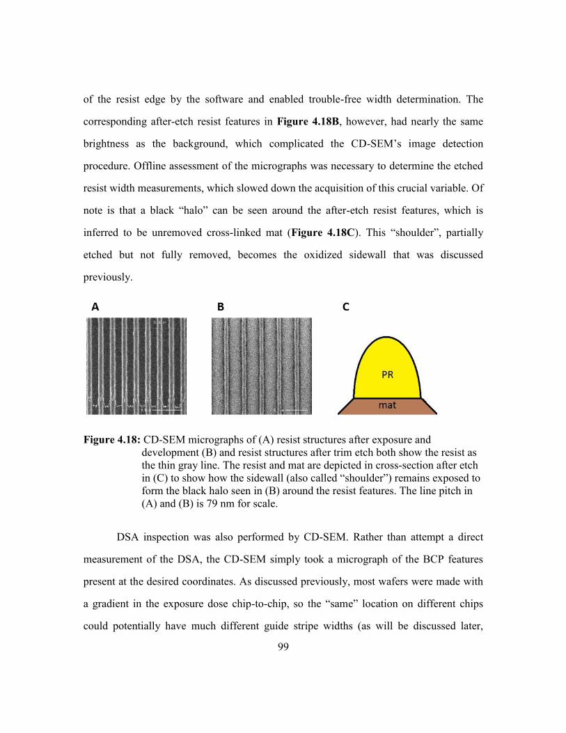
99
of the resist edge by the software and enabled trouble-free width determination. The
corresponding after-etch resist features in Figure 4.18B, however, had nearly the same
brightness as the background, which complicated the CD-SEM’s image detection
procedure. Offline assessment of the micrographs was necessary to determine the etched
resist width measurements, which slowed down the acquisition of this crucial variable. Of
note is that a black “halo” can be seen around the after-etch resist features, which is
inferred to be unremoved cross-linked mat (Figure 4.18C). This “shoulder”, partially
etched but not fully removed, becomes the oxidized sidewall that was discussed
previously.
Figure 4.18: CD-SEM micrographs of (A) resist structures after exposure and
development (B) and resist structures after trim etch both show the resist as
the thin gray line. The resist and mat are depicted in cross-section after etch
in (C) to show how the sidewall (also called “shoulder”) remains exposed to
form the black halo seen in (B) around the resist features. The line pitch in
(A) and (B) is 79 nm for scale.
DSA inspection was also performed by CD-SEM. Rather than attempt a direct
measurement of the DSA, the CD-SEM simply took a micrograph of the BCP features
present at the desired coordinates. As discussed previously, most wafers were made with
a gradient in the exposure dose chip-to-chip, so the “same” location on different chips
could potentially have much different guide stripe widths (as will be discussed later,

100
guide stripe width was a major factor in the quality of DSA). This necessitated imaging at
least half the wafer to ensure that the full range of guide stripe widths were sampled
(most wafers had symmetry about the x-axis removing the need to image the whole
wafer). Although the micrographs could be and were examined by hand, the need for a
quantitative method to compare different micrographs arose due to the sheer number of
micrographs taken and the subtle differences in DSA quality that emerged. A computer
program was written to evaluate an image for DSA quality, where the output was an
estimation of the percent of pixels in a micrograph “involved” in DSA (the program’s
algorithm is proprietary to Lam Research and unfortunately cannot be described here). As
seen in Figure 4.19, the scores produced by the program satisfyingly differentiated
between different degrees of DSA and thus were reliable metrics for DSA quality. Scores
of 100% were never observed, presumably due to ever-present line-edge roughness, and
defect-free micrographs of DSA typically scored 80 to 85%.
Figure 4.19: Representative micrographs of different degrees of DSA and their
corresponding score from the image scoring program.

101
The output of the image scoring program was often used to create a wafer map to
help determine trends across a wafer. A sample wafer heat map appears in Figure 4.20
and helps illustrate an important point about the results. This wafer, like the majority of
the samples, was produced with a dose gradient on the wafer (the right-hand side of the
wafer is high dose) to create a corresponding gradient of guide stripe widths. Since this
heat map represents the scores of micrographs taken at the same scatterometry target on
each chip, any variation in the scores in this heat map is almost entirely due to the guide
stripe width variation caused by the systematic exposure dose bias. Going from left to
right, two regions of “good” DSA can be clearly differentiated by their difference in color
from a region of “poor” DSA right down the middle of the wafer. Evidently, two
different regimes of guide stripe widths produce DSA. As shown in Figure 4.21, the two
regimes are anticipated to correspond to guide stripes pinning 0.5 and 1.5 L0 (10 and 30
nm) of BCP, and appear in both 4x and 5x density multiplication. The ability of the guide
stripe to pin different amounts of BCP based on its width was previously demonstrated by
the cross-section STEM experiment of the hybrid process presented in Figure 4.8, and a
further study of the guide stripe width for both the chemo-epitaxy and hybrid process
appears further on in the chapter. In the STEM experiment it was uncovered that the
hybrid process actually had a third regime of DSA (1 L0 guiding). However, this regime
performed worse than either 0.5 or 1.5 L0, and was omitted in subsequent studies. In
addition to the guide stripe width, the image scoring program was used to explore the
following process parameters: guide stripe pitch, guide stripe chemistry, brush chemistry,
BCP film thickness, anneal temperature, and anneal time. The micrographs presented in
Figure 4.7 and the comparisons made between the hybrid process and the chemo-epitaxy
process with either guide stripe material are the result of optimizing these parameters
separately for each process.

102
Figure 4.20: Representative heat map of DSA scores across one wafer with a dose
gradient applied (the right-hand side of wafer has the highest dose so
smallest guide stripe width). The two heat maps show the same data but are
printed in different color schemes.
Figure 4.21: Schematic of the anticipated DSA schemes on the wafer, labelled with the
density multiplication (either 4x or 5x) and the number of periods the guide
stripe width corresponds to (either W=0.5 or W=1.5).

103
4.8 QUANTITATIVE COMPARISON OF THE DSA PROCESSES
The DSA image scoring process was used to determine the optimal conditions for
each of the DSA processes, and then the optimized products were compared against each
other. This section describes a summary of the results, and then subsequent sections
describes the individual optimizations one-by-one.
4.8.1 Overview of the different DSA processes
XPMOST chemo-epitaxy was compared directly to XPS chemo-epitaxy. The
chemical similarity between the XPMOST guide stripe and the PMOST block of the BCP
was expected to result in a greater degree of anchoring between the two materials,
manifested in better DSA. Figure 4.22 shows that this hypothesis was true. Figure 4.22A
shows the two chemo-epitaxy processes under their final optimized conditions. In all
cases, XPMOST outperforms XPS to produce better DSA, supporting the guide stripe
strength argument. This effect is even more pronounced in Figure 4.22B, where the
conditions used to create both chemo-epitaxy wafers were far from ideal. (Section 4.11.2
describes the exact conditions used to make all three wafers). In this experiment, the
ability of the XPMOST to produce better DSA over XPS is clear. However, the
improvement in DSA scores for XPMOST in the best result for both cases, 4x density
multiplication with 0.5 L0 wide guide stripes, is negligible. To this effect, XPMOST
failed to produce a practical improvement over XPS in the criteria of overall defectivity.
The ability of XPMOST to produce better DSA than XPS for PMOST-b-PTMSS is
significant from a process window standpoint, but further optimizations in the process are
required to reduce defectivity.

104
Figure 4.22: Direct comparison of the chemo-epitaxy process with XPMOST and XPS
guide stripes at the four DSA schemes (A) under conditions optimized for
each process (B) under deliberately sub-optimal conditions.
One such attempt to reduce defectivity was the creation and implementation of the
hybrid process. This process largely mirrored the XPMOST chemo-epitaxy process, but
increased the thickness of the XPMOST guide stripe to produce topography. Figure 4.23
shows the results of increasing the thickness of the guide stripe. Wafers were prepared
identically except for changing the XPMOST mat coating thickness to 9, 15, and 19 nm
by changing the spin-coating speed. The 9 nm result corresponds to the chemo-epitaxy
process, and the two other thicknesses constitute the hybrid process. At 4x density
multiplication, the DSA scores increased monotonically with increasing guide stripe
thickness, and produced among the highest DSA scores recorded. The results were less
consistent at 5x density multiplication, but since this region of the wafer performed worse
than the 4x region overall, the implementation of the hybrid process was deemed an

105
overall success. Going forward, all instances of the hybrid process used a 19 nm thick
guide stripe.
Figure 4.23: Comparison of the hybrid process to the chemo-epitaxy process. The 9 nm
data correspond to the chemo-epitaxy process made with XPMOST, while
the other two thicknesses correspond to hybrid process with XPMOST.
Error bars are 3 standard deviations.
4.8.2 Guide stripe pitch
The effect of the pre-patterned guide stripe pitch on DSA was investigated by
comparing DSA scores taken at different pitches in the vicinity of 100 nm on the same
wafer. The bulk periodicity of the BCP was determined to be approximately 19.7 nm by
SAXS taken at room temperature of a sample annealed at 180 °C. A fast Fourier
transform (FFT) of the fingerprint BCP pattern, made and imaged on IMEC CD-SEMs,
was also performed as seen in Figure 4.24. The peak location in the FFT was determined
to be 19.3 to 19.6 nm, corroborating the SAXS value. Therefore, pitches near and slightly
below 100 nm were anticipated to capture the 5x density multiplication regime. Figure
4.25 shows a statistical summary of the DSA scores of pitches near 100 nm taken from a

106
single wafer prepared with the chemo-epitaxy process (XPS guide stripes). A clear trend
in the DSA quality emerges, with a DSA score maximum centered around a pitch of 98
nm (the scores at 97 and 99 nm are not statistically different, however). If one assumes
the best DSA occurs when the pre-pattern pitch is most commensurate with the natural
periodicity of the BCP, a value of 98 nm implies the effective thin film L0 of the BCP is
19.6 nm, which agrees well with the values determined by the two other methods.
Figure 4.24: (A) Top-down SEM of fingerprint pattern of ~20 nm BCP (B) 2D fast
Fourier transform (FFT) of the image in (A). FFT software provided
courtesy of http://www.ejectamenta.com.

107
Figure 4.25: DSA score versus pre-pattern pitch of a chemo-epitaxy process wafer made
with XPS. The data were taken from the region where the guide stripe
pinned approximately 0.5 L0 of BCP. The box plot represents the five
number summary of the data.
The pre-pattern pitch was also investigated at approximately 80 nm to probe the
4x density multiplication regime. Figure 4.26 shows the results from a hybrid process
wafer. Unfortunately, the quality of the resist structures degraded markedly below 78 nm,
so only pitches of 78, 79, and 80 nm were compared. Results are included from the
region on the wafer corresponding to where the guide stripe pins 0.5 L0 (Figure 4.26A)
and 1.5 L0 (Figure 4.26B). The 1.5 L0 DSA scores are higher than the 0.5 L0 scores, and
both are higher than the sub-optimal XPS chemo-epitaxy results reported in Figure 4.25.
In Figure 4.26B it appears that 79 nm performed slightly better than 80 nm, but the
relationship is flipped in Figure 4.26A. Both pitches scored better than 78 nm, even
though 78 nm is closer to the “magic” BCP L0 value of 19.6 nm determined for the 5x
density multiplication (78 / 4 = 19.5, 79/4 = 19.75, 80/4 = 20). The DSA quality trend
due to pre-pattern pitch at 4x density multiplication is less conclusive than the same
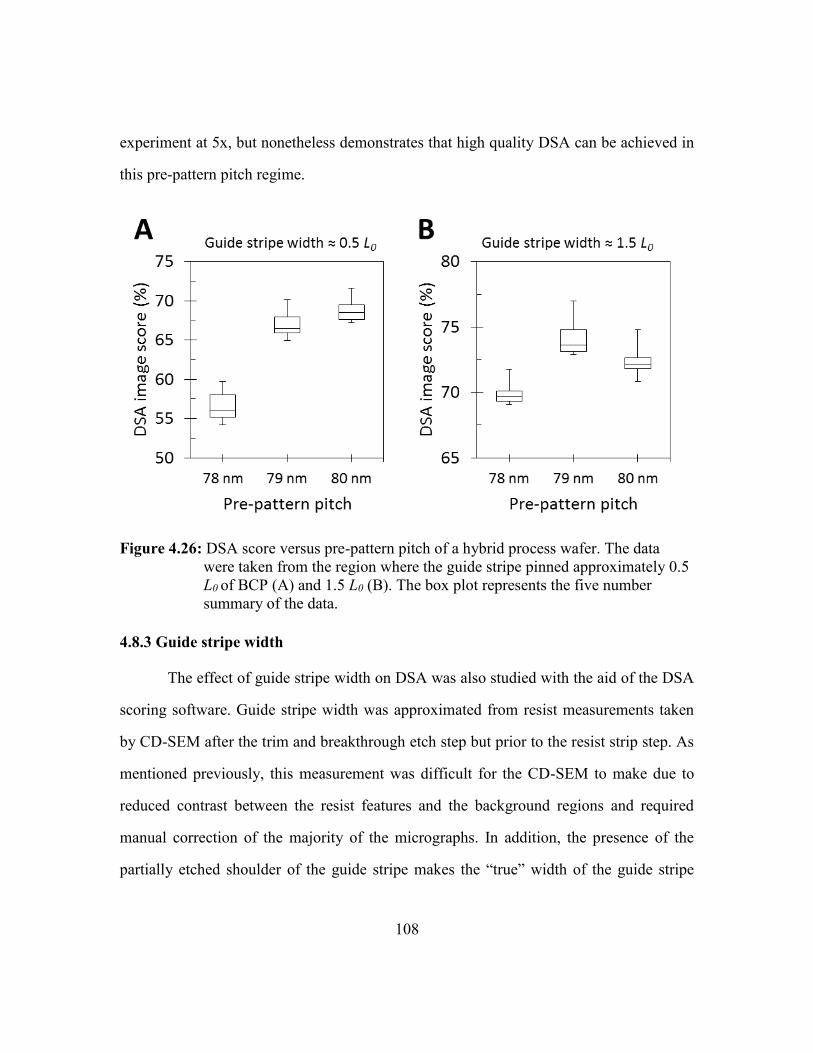
108
experiment at 5x, but nonetheless demonstrates that high quality DSA can be achieved in
this pre-pattern pitch regime.
Figure 4.26: DSA score versus pre-pattern pitch of a hybrid process wafer. The data
were taken from the region where the guide stripe pinned approximately 0.5
L0 of BCP (A) and 1.5 L0 (B). The box plot represents the five number
summary of the data.
4.8.3 Guide stripe width
The effect of guide stripe width on DSA was also studied with the aid of the DSA
scoring software. Guide stripe width was approximated from resist measurements taken
by CD-SEM after the trim and breakthrough etch step but prior to the resist strip step. As
mentioned previously, this measurement was difficult for the CD-SEM to make due to
reduced contrast between the resist features and the background regions and required
manual correction of the majority of the micrographs. In addition, the presence of the
partially etched shoulder of the guide stripe makes the “true” width of the guide stripe

109
ambiguous. Figure 4.27 shows a zoomed-in CD-SEM micrograph and highlights these
points.
Figure 4.27: CD-SEM micrograph of the resist features highlighting the approximate
resist edge and the presence of the partially etched guide stripe.
After measuring the width of the guide stripes, the DSA process was completed,
and the wafer was imaged by CD-SEM. The DSA scores calculated from these
micrographs were then mapped to the previously measured guide stripe widths to create
Figure 4.28. Figure 4.28A is the correlation of DSA scores on guide stripe width for an
XPS chemo-epitaxy process wafer, and Figure 4.28B is the same relationship for a
hybrid process wafer. These results were measured at 79 nm guide stripe pitch (4x
density multiplication), and the results at 98 nm pitch (5x density multiplication) are
qualitatively similar. XPMOST chemo-epitaxy results also mirror the XPS chemo-
epitaxy results. A striking number of contrasts emerge from these graphs. First, the
relationship for the chemo-epitaxy process is approximately parabolic and has a
maximum between 16 and 20 nm. The DSA scores in the hybrid process, however, are
almost uniformly high from 7 to 16 nm, and actually dip to their lowest values at the
guide stripe widths that produce the highest scores for the chemo-epitaxy process. In

110
addition, Figure 4.28B captures the start of the 1.5 L0 guide stripe DSA regime at
approximately 24 nm for the hybrid process, while in Figure 4.28A this regime is absent,
although the window is known to exist at guide stripe widths closer to 30 nm for the
chemo-epitaxy process. It appears that in addition to producing higher overall higher
scoring DSA micrographs, the hybrid process is much more tolerant of variation in the
guide stripe width than the chemo-epitaxy process.
Figure 4.28: DSA score versus guide stripe width for (A) XPS chemo-epitaxy process
wafer (B) hybrid process wafer for 20 nm PMOST-b-PTMSS at 79 nm
guide stripe pitch (4x density multiplication).
The ideal guide width is expected to be 10 nm (0.5 L0) in the chemo-epitaxy
process in this guide stripe width regime, however the measured maximum appears
between 0.8 and 1.0 L0. Some of this 6 to 10 nm deviation from 10 nm could likely be
attributed to the uncertainty between the resist and guide stripe width measurement, as
discussed previously. However, other research has also documented the preference of

111
guide stripes wider than 0.5 L0 in the chemo-epitaxy DSA of PS-b-PMMA.121,122 This
explanation could account for the wider than expected guide stripes, even though the
deviation seen here is larger than that seen for PS-b-PMMA (typically reported as 0.6-0.8
L0). Also possible, but less likely, is the hypothesis that the guide stripe actually pins 1.0
L0 of BCP. This hypothesis would explain why the ideal guide stripe width is closer to 20
nm than it is to 10 nm. However, it does not explain the absence of any indication of 0.5
L0 guide stripe DSA, which would still be expected to occur even if 1.0 L0 was the
predominant DSA scheme. In addition, the only previous account of 1.0 L0 DSA by
Cushen97 describes the need for a large degree of topography for the 1.0 L0 DSA to occur,
which is absent in the chemo-epitaxy process. A cross-sectional analysis of the DSA in
the chemo-epitaxy process could potentially clear up this situation, but the experiment
would have to be performed in such a way that the guide stripe boundary was
discernable, which was not the case in the STEM EELS experiments used to probe the
hybrid process.
4.8.4 Backfill brush composition
Three candidate PS-r-PtBuS hydroxyl-terminated brushes, representing a range of
surface energies, were screened for DSA behavior in both processes to determine the
optimal brush composition (the fourth brush, introduced in Table 4.1, was determined to
be outside of the range of surface energies needed for DSA and largely ignored). The
surface energy of the backfill brush used in a DSA process must be precisely tuned to
produce the best DSA.59 The optimum brush surface energy for DSA, however, is
different from the surface energy that is non-preferential to the bulk BCP.59,63 Due to the
unequal number of BCP domains that interface with the region defined by the backfilled
brush (for n density multiplication, where one PMOST block is pinned by the guide

112
stripe, the ratio of PMOST to PTMSS in the backfill region is n – 1 : n), the backfill
brush deviates from neutrality in the direction of the majority block to compensate for
asymmetry, and Nealey et al. suggest that the ideal backfill brush surface energy is
“neutral” to the weighted average of the BCP domains interfacing with the backfill
brush.59 However, complex substrate-BCP interactions,45 substrate reorganization
effects,123 and the sensitivity of surface energy to small chemical changes56 preclude any
diagnostic test of the brush outside of actual DSA implementation. To this effect, as
described previously, a series of functionalized brushes were prepared with different feed
amounts of PS and PtBuS (Table 4.1) to test DSA performance. The brush samples are
labelled as BB-nn, where nn is the mole percent of PS in the brush, measured by NMR.
Since PS has a higher surface energy than PtBuS, higher PS content results in a more
hydrophilic and higher surface energy brush. As described previously, island-hole118
experiments determined that BB-85, the sample with highest PS content, is
approximately neutral for the BCP,63 while BB-50 and BB-68, with more PtBuS content,
are PTMSS wetting. To test these brushes, XPS guide stripe chemo-epitaxy wafers were
made with each brush and inspected. DSA was observed on the wafer produced with
slightly-preferential BB-68 brush, no BCP features were seen on the wafer made with the
more preferential BB-50 brush (it is expected that the BCP features were aligned parallel
to the substrate), and BCP fingerprint pattern without DSA was observed on the wafer
produced with neutral BB-85 brush. Evidently, these three brushes bracket the range of
relevant surface energies for DSA, and the composition and surface energy of slightly-
preferential BB-68 brush is close to ideal for DSA.
To further hone in on the ideal backfill composition, the brushes were mixed to
yield blends with compositions intermediate to the parent polymers. This blending
strategy is not new; Nealey et al. reported that blending homopolymer brushes of PS and

113
PMMA yielded blends with wetting properties proportional to the amount of PS and
PMMA in the blend,124 so it was reasoned that blending different PS-r-PtBuS brushes
was a valid way to produce substrate-modifying materials with surface tensions
intermediate to that of the parent brushes. The DSA scores with several brush
compositions are shown in Figure 4.29A for XPS guide stripe and Figure 4.29B for
XPMOST guide stripe. Compositions in bold indicate pure brush and refer to the
corresponding BB-nn sample, while compositions in italics indicate a blended brush,
described in Table 4.2. Comparing Figures 4.29A and 4.29B, the ideal brush
compositions are surprisingly different for the two guide stripe chemistries. Compared to
the ideal brush composition for XPS, 71% PS, the ideal brush composition for XPMOST
is more hydrophobic at approximately 68%. Apparently, to compensate for the higher
surface energy XPMOST guide stripe, a lower surface energy brush is required. This
observation suggests that there is an additional relationship between the guide stripe and
brush surface energies yet to be explicitly quantified. BCP wetting behavior, elucidated
from island-hole studies, serves as a guide for design of backfill brush but at this point,
the ideal backfill brush chemistry for DSA must be empirically determined.

114
Figure 4.29: DSA image score versus backfill brush at 4x density multiplication with 0.5
L0 guide stripes for (A) XPS guide stripe chemo-epitaxy process and (B)
XPMOST guide stripe chemo-epitaxy process. Compositions in bold are
pure polymers and compositions in italics are blends. The boxplots represent
the five number summary of the data.
Table 4.2: Weight % composition of the brush formulations used in Figure 4.29.
Sample Composition % BB-50 % BB-68 % BB-85
66 10 90 0
68 0 100 0
71 0 84 16
73 0 70 30
85 0 0 100
B
0
10
20
30
40
BB3 16% BB4,84% BB3
30% BB4,70% BB3
BB4DSA
imag
e sc
ore
(%
)
Backfill brush formulation (% PS)
XPS Guidestripe
A
68 71 73 85
20
30
40
50
60
70
10% BB2, 90%BB3
BB3 16% BB4, 84%BB3
DSA
imag
e sc
ore
(%
)
Backfill brush formulation (% PS)
XPMOST Guidestripe
66 68 71

115
There was no statistically significant difference between using BB-71, optimal for
XPS chemo-epitaxy, and BB-68, optimal for XPMOST chemo-epitaxy, in the hybrid
process. Since the process worked equally well with either brush composition, a thorough
optimization was not performed. For all experiments with the hybrid process, BB-68, the
optimal XPMOST chemo-epitaxy brush, was used.
4.8.5 BCP film thickness
The film thickness (t) of the BCP was determined to be a primary contributor
towards DSA quality and was studied by systematically varying t from approximately 1.0
to 2.5 L0 on wafers patterned with XPS guide stripes. As seen in Figure 4.30, varying the
t caused the average DSA scores to vary substantially from 45 to 65% in a periodic
fashion. Three local score maxima are seen at approximately t = 1.2, 1.7, and 2.4 L0, with
corresponding minima at approximately t = 1.2, 1.3, and 2.1 L0. Smaller BCP t values
resulted in better DSA for PS-b-PMMA,125,126 but this is the first documentation of a
periodic dependency of the DSA performance on t. Curiously, other BCP behaviors in
thin films have a periodic dependency on film thickness. For example, the perpendicular
orientation of BCPs in thin films can be preferred at certain film thicknesses due to the
delicate interplay between conformational entropy and surface energy effects.42,43,50,65
Such phenomenon are likely at play here due to confinement effects (both in thickness
and in-plane), and further modeling studies are needed to understand the interdependence
of BCP t and DSA.

116
Figure 4.30: DSA score versus nondimensionalized BCP film thickness for a series of
XPS chemo-epitaxy wafers. The points represent average scores and the
error bars represent maximum and minimum values for 4x density
multiplication and circa 0.5 L0 guide stripe width.
An interesting phenomenon emerges when the data is examined not just for 4x
density multiplication with 0.5 L0 wide guide stripes, which is the DSA scheme that
scored the best for this process, but also for the other three schemes. Figure 4.31
summarizes a subset of the data presented in Figure 4.30, with the addition of the results
for DSA with 1.5 L0 wide guide stripes, as well as 5x density multiplication. As
explained, 4x density multiplication with 0.5 L0 wide guide stripes produced the best
results, but surprisingly, 5x density multiplication with 1.5 L0 wide guide stripes scored
nearly as high and came in a clear second. The only immediate connection between the
seemingly opposite DSA schemes is that both have the same number of BCP domains
(which amounts to the same ratio of components) sitting in the brush backfill region, as
shown in Figure 4.21. As was discussed in the polymer brush section, the brush must be
chosen specifically for the BCP components that interface with the backfill region, and

117
the brush used for this experiment was the composition found to produce the best DSA in
4x density multiplication with 0.5 L0 wide guide stripes, which by our understanding
could also be the ideal brush for DSA with 5x density multiplication and 1.5 L0 wide
guide stripes, and helps to explain these results. Since the brush is necessarily sub-
optimal for the other two DSA schemes, it makes sense that the DSA in those regions
performs poorly.
Figure 4.31: A subset of the DSA score versus nondimensionalized BCP film thickness
for series of XPS chemo-epitaxy wafers. The points represent average scores
and the error bars represent maximum and minimum values for the four
DSA regimes identified on the wafer.
The same analysis was also applied for the hybrid process. Figure 4.32 shows the
DSA score versus BCP film thickness for three DSA schemes (5x density multiplication
with 0.5 L0 wide guide stripes performed the worst and was omitted for clarity). In the
range of BCP film thicknesses investigated, there was a much smaller variation in DSA
score than in the XPS chemo-epitaxy study. There is some indication that again the film
thicknesses commensurate with the BCP’s L0 (1.5 and 2.0 L0) produce the worst DSA,

118
but this effect is less pronounced than for XPS chemo-epitaxy. Most surprising is that 4x
density multiplication with 1.5 L0 wide guide stripes produced the best DSA results,
instead of either of the two DSA schemes previously identified as working the best in
chemo-epitaxy. The reason for this change is not immediately obvious but could again be
potentially attributed to the brush chemistry used to make the wafer.
Figure 4.32: DSA score versus nondimensionalized BCP film thickness for series of
hybrid process wafers. The points represent average scores and the error
bars represent maximum and minimum values for the three identified DSA
schemes. 5x W=0.5 is omitted for clarity, but performed the worst overall.
4.8.6 Annealing time and temperature
The process variables of annealing time and temperature were examined with the
DSA image scoring technique. Optimizing the aforementioned process parameters
decreased but did not eliminate defects, chief among them dislocation defects where the
BCP strays from the pre-pattern for only a few periods. Defects are thermodynamically
unstable127 but annihilation of defects is a kinetic process.128,129 Studying the effect of

119
anneal time and temperature on the DSA was performed to better understand the
importance of these parameters on defectivity.
Wafers with the same XPS chemo-epitaxy process were made and annealed at
170°C, 180°C, 190°C, and 200°C. Temperatures above 215°C caused the top coat film to
dewet from the underlying BCP, as seen in Figure 4.33. The top coat is inherently
unstable on top of the BCP, but when annealed only below its glass transition
temperature (Tg), the top coat lacks the mobility to dewet. Dynamic scanning calorimetry
(DSC) measured the Tg to be approximately 200 to 210°C,39 further corroborating that
annealing at or above the Tg of the film leads to dewetting.
Figure 4.33. Optical micrograph of an XPS chemo-epitaxy wafer with a completed DSA
film stack after being annealed at 215°C for 5 minutes. The spots are top
coat dewetting from the BCP surface.
The samples annealed at 170°C and 180°C produced DSA with many regions
believed to be horizontally oriented BCP lamellae (Figure 4.34). Although many
micrographs showed indication of alignment with the underlying substrate, these areas
surrounded gray regions of parallel features. Samples annealed at 190°C and 200°C did
not suffer from these patches. The 170°C sample was remade and annealed for an
additional 70 minutes to confirm the areas were not a processing mistake (Figure 4.34A).

120
Even with the longer anneal, the gray regions persisted. Closer examination of these
defect regions (Figure 4.34B) showed what appears to be correctly oriented BCP
domains nucleating from the gray regions. Since the substrate consists of alternating
bands of material that preferentially wet different components of the BCP, perhaps the
mechanism by which DSA occurs involves a step where some patches of the BCP
initially orient themselves parallel to the substrate, and only gradually orient themselves
perpendicularly. Taking “snapshots” of the DSA process by annealing several wafers at a
temperature where the gray regions were previously not witnessed (>190°C) for short
time increments could potentially capture this process in action. Taking real time
micrographs of the surface using a non-destructive imaging technique like AFM could
also accomplish this goal, if a technique was discovered that could image the BCP
features through the top coat.

121
Figure 4.34: SEM micrographs of (A) XPS chemo-epitaxy process annealed at 170°C for
70 minutes and (B) the same film stack annealed at 180°C for 10 minutes.
(B) is enlarged to show mark areas BCP domains are beginning to nucleate
from the horizontal features.
The samples annealed at 190°C and 200°C for 10 minutes produced DSA without
the gray patches and the DSA was analyzed by the image scoring software. Figure 4.35
summarizes these results. In all cases, the 200°C sample produced a superior DSA result.
Besides imbuing the BCP with additional thermal energy to cure defects, it is not obvious
if there is an additional mechanism by which raising the temperature leads to lower
defectivity. Surface tension, which governs a number of important interactions in BCP
DSA, is a function of temperature, and the rate of surface tension change is different for
every polymer. It is possible that changing the temperature causes the surface tensions of
the guide stripe, the brush, and the BCP to become better matched for DSA, but it is not
clear how to isolate these effects for further study. Since annealing at 200°C worked
better than 190°C, but annealing at 215°C becomes problematic due to the Tg of the top
coat, an annealing temperature in-between these two, 205°C, was chosen for every other

122
DSA experiment. No indication of top coat dewetting was seen at 205°C, even after
annealing for one hour at this temperature.
Figure 4.35: DSA score versus temperature for the four DSA schemes on an XPS
chemo-epitaxy wafer. Error bars are 3 standard deviations
To further probe the kinetics of DSA defectivity, two XPS chemo-epitaxy wafers
were prepared identically, and one was annealed for 5 minutes and the other was
annealed for 60 minutes. The summary of the DSA image score analysis appears in
Figure 4.36A. These wafers were prepared with an exposure that did not print the pre-
pattern at 4x density multiplication, so only the regions containing 5x density
multiplication were compared. The DSA score when the guide stripe width = 0.5 L0 was
much worse than when width = 1.5 L0, but this region also experienced the larger
increase in DSA quality after the longer anneal. Figure 4.36B compares micrographs of
the “best” DSA from this “worse” region at 5 and 60 min, showing how the longer anneal
resulted in fewer dislocation defects and much longer segments of uninterrupted DSA
patterns. Compared to this result, the improvement in DSA quality at the “better” region
of width = 1.5 L0 was marginal. A statistically significant difference arose between the
top scores of this region at the two anneal durations, but the micrographs from the two

123
anneal times display little in terms of a practical difference. The number of dislocation
defects are decreased but not eliminated at the longer annealing time.
Figure 4.36: (A) DSA score versus annealing time (at 205°C) for two DSA schemes on
an XPS chemo-epitaxy wafer. (B) Representative micrographs of best DSA
result from the 5x W=0.5 region demonstrating the improvement upon
annealing longer.
4.9 CONCLUSIONS AND FUTURE WORK
In conclusion, the DSA of a sub-20 nm silicon-containing BCP was implemented
at IMEC. Materials suitable for the control of the BCP were synthesized at UT and
introduced into IMEC’s 300 mm cleanroom. Two different processes were used for DSA.
A hybrid process was designed to use shallow topography as well as chemo-epitaxy as
guiding surfaces, and was compared to a more traditional chemo-epitaxy process. In
general, the hybrid process achieved higher DSA quality than the corresponding chemo-
epitaxy process, and the process window for a number of parameters was larger as well.
Cross-section STEM EELS experiments demonstrated the BCP features travel vertically
through-film, without forming any complex 3D morphologies, despite the presence of the

124
shallow topography. The sidewall of the guide stripe is anticipated to play a large role in
aligning the BCP features.
This is only the second account- after PS-b-PMMA- of the DSA of a BCP using
processes suitable for HVM. The optimizations described in previous sections should
provide a roadmap for the DSA of future materials using similar processes, regardless of
material chemistry.
Experiments are underway at IMEC to follow up on the work presented in this
chapter. A guide stripe material containing a nitrogen in the repeat unit has been
synthesized and introduced into IMEC to enable precise determination of the BCP/guide
stripe interface in STEM with EELS experiments. The integration of silicon-containing
BCPs smaller than 20 nm is also planned, which also entails a need for a double-
patterned sidewall DSA scheme as discussed previously.
4.10 ACKNOWLEDGEMENTS
The DSA described here was performed at IMEC, Leuven, Belgium. The work
was made possible by generous support from Lam Research Corporation, managed by
Diane Hymes. Stephen M. Sirard of Lam also contributed as technical consult. The Lam
office at IMEC, managed by Johan Vertommen, contributed greatly to the effort, above
and beyond their official roles. David Hellin, Mohand Brouri, Christophe Noben, and
Bart Coenegrachts specifically helped with etch recipes and logistics and deserve special
recognition for their contributions. Geert Vandenberghe generously managed the IMEC
portion of the collaboration. Roel Gronheid, Paulina Rincon Delgadillo, BT Chan, Nadia
Vandenbroeck, Hari Pathangi, Arjun Singh, Robert Seidel, Jan Doise, and Grant Garner
contributed to the DSA research from IMEC. Rikimaru Sakamoto, Yasanobu Someya,

125
and Hiroyuki Wakayama, all of Nissan Chemical, contributed to the collaboration.
Michael J. Maher, Yusuke Asano, and Andrew Dinhobl contributed to material synthesis.
4.11 EXPERIMENTAL
4.11.1 Processing
Samples were prepared on commercial 300 mm wafer handling equipment at
imec as previously described.111,116 Si wafers with 13 nm of silicon nitride as an anti-
reflective coating were coated with 8 nm of XPS mat or 8 or 19 nm of XPMOST mat and
annealed at 315 °C for 5 min under nitrogen to cross-link. Wafers were coated with
commercial AIM5484 resist and exposed by an ASML 1950 or 1970 193i scanner. After
development, resist features were trim etched in a Lam Research Kiyo® conductor etch
chamber. Resist was stripped with Orgasolv in a TEL ACT12 track. Hydroxyl-terminated
brush (1% w/v propylene glycol monomethyl ether acetate) was manually spin-coated in
the same ACT12 track. The brush was annealed under nitrogen at 250 °C and then
ungrafted brush was stripped by RER 600 organic solvent. PMOST-b-PTMSS (1% w/v
methyl isobutyl ketone) was manually spin-coated to give a film thickness of 30-35 nm
(1.6 to 1.8 L0). Top coat in the form of a ring-opened trimethylamine salt (0.5% w/v
methanol) was spin-coated directly on top of the BCP. The wafer was then annealed at
205 °C for 5 minutes. The wafer was then etched in a Lam Research Flex™ dieletric etch
chamber. Inspection was performed by Hitachi Hi-Tech CG4000 and CG5000 CD-SEMs.
Cross-sectional STEM images with EELS mapping were provided by Nanolab
Technologies.

126
4.11.2 Conditions for each DSA process
Table 4.3: Summary of processing conditions used to make Figure 4.7
Process step XPS chemo- XPMOST chemo- Hybrid
Mat deposition Commercial NLD-
128 = 8 nm
XPMOST 0.5 wt.%
PGMEA 3000 RPM
= 9 nm
XPMOST 0.5 wt.%
PGMEA 600 RPM
= 19 nm
Brush composition
(see Table 4.2)
BB-71 BB-68 BB-68
BCP deposition 1.2 wt. % MIBK
1500 RPM = 33 nm
1.2 wt. % MIBK
1500 RPM = 33 nm
1.2 wt. % MIBK
1500 RPM = 33 nm
Top coat deposition 0.5 wt. % methanol
1500 RPM = 19 nm
0.5 wt. % methanol
1500 RPM = 19 nm
0.5 wt. % methanol
1500 RPM = 19 nm
Anneal 205°C 5 mins 205°C 5 mins 205°C 5 mins
CD to image for best
feature formation
18 nm 18 nm 14 nm

127
Chapter 5: Direct self-assembly for bit patterned media applications
The work in this chapter has been reproduced in part with permission from a
manuscript prepared by Lane, A.P.; Yang, X.; Maher, M.J.; Blachut, G.; Asano, Y.;
Someya, Y.; Mallavarapu, A.; Sirard, S.M.; Ellison, C.J.; Willson, C.G.; “Directed self-
assembly of 5 nm Block Copolymer Lamellae” (to be submitted). For this manuscript, the
author synthesized polymeric surface treatments, and designed and carried out
experiments.
5.1 BACKGROUND
Another pattern-densification application of the directed self-assembly (DSA) of
block copolymers (BCPs) is bit patterned media (BPM) for hard disk drives (HDD). In
direct analogy to the transistor density scaling described by Moore’s Law,3 Kryder’s Law
describes the scaling of the areal density of magnetic media in HDDs.130 Impressively,
the data stored on a HDD increased 1,000-fold from 1990 to 2005 by continual
refinements to the technology used to make the magnetic head, which addresses the data,
and the magnetic media, which stores the data.130 However, a decade later, an overhaul of
HDD technology is required to continue this aggressive scaling.
As described by the Advanced Storage Technology Consortium (ASTC)
roadmap,131 a “new paradigm” will be necessary in order to make next-generation
devices with more storage density. The need for such a technological switch has become
even more pressing as solid-state flash memory emerges as a viable alternative to HDDs
for storage media in high-tech devices.132 The limitations of current HDD technology are
largely a consequence of the limited storage density of the current magnetic media. So-
called conventional multigrain media (CMM) stores bit of data by grouping individual
magnetic grains together to make a weakly-coupled magnetic cluster. The density of data

128
storage is, therefore, inversely proportional to the size of each grain times the number of
grains that constitute a bit. Decreasing the number of grains in a bit also decreases the
signal-to-noise ratio of the magnetic media,133 and decreasing the area (or volume) of
each grain allows the magnetic moment of the grain to spontaneously flip (the so-called
superparamagnetic effect) with increased likelyhood.134 State-of-the-art, 1 terabit/in2
(Tb/in2) devices operate essentially at the limit of both of these constraints.133 New
technologies are needed to circumvent these physical limitations.
The technology with the most support from the HDD industry is heat-assisted
magnetic recording (HAMR). Since the superparamagnetic effect limits the size of the
grains, using a magnetic material with a higher coercivity, or resistance to magnetic
flipping, will allow the use of smaller grains.135 However, the higher coercivity makes
each grain prohibitively difficult to rewrite at room temperature. To circumvent this
coercivity “catch-22”, HAMR uses a laser to locally heat the magnetic material, making
the grains more susceptible to magnetization.135 Implementation of HAMR is contingent
on the resolution of numerous technical difficulties, including the reliability of the laser
used to heat the media, the reliability of the lubrication layer used to protect the media,
and many other practical concerns.
Instead of making the grains more resistant to spontaneous demagnetization, BPM
physically isolates the grains of a bit from neighboring bits to increase magnetic stability
without requiring an overhaul of the materials used in the head or the storage media. In
CMM, the volume of a magnetic element is essentially the volume of an individual grain,
while in BPM each grain can be magnetically coupled to its neighbors, making the
combination of grains the effective volume.11 This greatly decreases the threshold volume
needed for stable storage, which increases the areal density of the HDD. The trade-off is

129
that the magnetic media needs to be lithographically patterned to create the isolated
magnetic islands that form the bits.
A geometric analysis reveals that 1 Tb/in2 BPM patterns, which are approximately
equivalent to the storage density limit of CMM, require the center to center distance of
each bit be approximately 25 nm. To produce patterns with 10 Tb/in2 storage density,
which is the long term vision of the ASTC roadmap,131 the center to center distance needs
to be approximately 8 nm. Both of these pitches are well beyond the resolution capability
of state-of-the-art 193 immersion lithography (193i) used for the high volume
manufacturing of integrated circuits (approximately 80 nm full pitch).12 Step-and-flash
Imprint Lithography (SFIL), now commonly known as Nanoimprint Lithography (NIL),
has sufficient resolution capability10 and throughput needed for high volume
manufacturing,11 but is gated by the availability of a master template with 25 nm or 8 nm
full pitch features. Electron beam lithography (EBL) has sufficient resolution to make
features this small for a template,108 but making a full template would take at least one
month,102 at which point beam stability issues would significantly impact the quality of
the produced template.
In much the same way that BCP DSA can multiply the frequency of 193i, BCP
DSA can be used to multiply the density of an initial EBL-patterned template to produce
a final NIL template with sufficient density for BPM. Many proof-of-concept
demonstrations of BPM using DSA have been reported by Hitachi Global Storage (now
Western Digital),67,136 Toshiba,137 and Seagate.138 However, much work remains to be
done to reach the scaling goals for this technology. Although the concept of magnetically
isolated islands evokes images of cylindrical pillars, research suggests that the best shape
for BPM features would be rectangular11,68 in order to exploit the spatial anisotropy of a
magnetic head. These features can be made by aligning BCP lamellae in one direction,

130
and then applying a second pattern of different pitch that is oriented perpendicular to the
original pattern, as shown in Figure 5.1.
Figure 5.1: Fabrication of rectangular patterns from BCP lamellae. In D and E, a second
patterning step is used to chop the line space pattern into discreet rectangles.
Used with permission from Ruiz, R.; et al. ACS Nano 2011, 5, 79–84.
Copyright 2011 ACS.
To facilitate the development and mass production of NIL templates, Seagate has
developed a two-step NIL and DSA process.139 A “seed” NIL template (with sparse
patterns produced by EBL) is patterned onto a substrate, and then the DSA process is
performed on this pattern. The product wafer, now with a much denser pattern, is then
used to make a second NIL template, which functions as the master template for BPM
production. This route minimizes the reliance on EBL patterns for research and
development. Although the cited reference demonstrated DSA with cylinder-forming
BCPs, the process is general enough to be compatible with a number of different DSA
materials, including lamellae.
The rest of this chapter details the collaboration between Seagate and the
University of Texas to develop a DSA process with the silicon-containing, high-χ
materials previously discussed. Some of the learning from IMEC was used to aid in the

131
process development, but the nuances of working with NIL necessitated new procedures
to solve new problems.
5.2 PROCESS OVERVIEW
Figure 5.2 shows the materials and processes used in conjunction with the
Seagate NIL patterns. The 10 nm BCP used for the project, depicted in Figure 5.2A, is
poly(5-vinyl-1,3-benzodioxole-b-4-pentamethyldisilylstyrene) (PVBD-b-PDSS). As
discussed in Chapter 3, this BCP chemistry has a χ value large enough to access 10 nm
full pitch feature, yet the polar component is not soluble in methanol, allowing the top
coat surface neutralization strategy to be employed. The hydroxyl-terminated PS-r-PtBuS
brushes developed for the IMEC project were also introduced at Seagate, and the
chemistry is depicted in Figure 5.2A.
Figure 5.2: The (A) materials and (B) process steps used for producing 10 nm DSA in
the NIL process. Arrow 1 and 2 describe the process with and without a
grafted brush, respectively.

132
In the standard process, a 150 mm wafer was patterned by NIL using a
commercial acrylate-based resist and a template containing approximately 18 nm line
widths in a matrix of 40 to 50 nm full pitches. Occasionally, the wafer was coated with 2-
3 nm of sputtered chromium, a standard mask material for manufacturing NIL templates,
and the NIL step was performed on top of this layer. The NIL pattern was then etched
with an oxygen-based reactive ion etch (RIE) to clear out the approximately 8 nm-thick
residual layer of NIL resist remaining between the guide lines. Since this “breakthrough”
etch also trimmed down the height and width of the NIL guide lines, typically each
quadrant of a wafer was etched for different times to vary the extent of resist trimming.
At this point, a polymeric brush was sometimes applied, but as will be discussed, a
degree of success was achieved without this step as well. In Figure 5.2B, the arrow
labelled 1 shows the process with the brush deposition step, and the arrow labelled 2
shows the process without the brush deposition step. After the brush was applied and
annealed, the BCP was then spin coated out of methyl isobutyl ketone (MIBK), and the
trimethylamine salt of the top coat39 was spin coated out of methanol. The wafer was then
heated to anneal the BCP and to ring-close the top coat and produce a neutral interface
for the BCP. This anneal also imparts mobility into the BCP, which enables DSA,
presumably by a hybrid chemo-/grapho- epitaxy mechanism where the polarity and
topography of the resist lines drives the correct assembly of the BCP. To image the BCP,
a second O2 RIE step was then used to remove the top coat and lightly decorate the BCP
features.
The LiNe-style chemo-epitaxy process could not be replicated exactly because
was impossible to do with the NIL resist since there is no way to strip the cross-linked
NIL resist from an underlying polymer mat (which would then function as guide stripes).
Thus, the resist lines themselves had to be used as guide stripes.140 However, one

133
unanticipated issue emerged with the brush deposition step as a result. It was discovered
that, unlike for the cross-linked poly(4-methoxystyrene) (XPMOST) and poly(styrene)
(XPS) guide stripes used in Chapter 4,97 the brushes did indeed graft appreciably to the
etched NIL resist. As Figure 5.3 shows, a pre-pattern treated at 200 °C with a neutral
brush produces only poorly aligned BCP domains, and importantly, the domains seem to
align mostly perpendicular to the direction of the NIL resist lines. Apparently, the brush
was grafted more-or-less uniformly on both the exposed silicon oxide surface and the
etched resist, producing no highly preferential surfaces that would direct the assembly
along the guide stripe direction. This result prompted a new strategy for mitigating the
grafting promiscuity of the brushes.
Figure 5.3: Top-down SEM of 10 nm PVBD-b-PDSS on etched NIL resist with a neutral
brush grafted at 200 °C for 10 minutes. The resist lines run vertically, while
the BCP domains travel mostly horizontally. The patchy regions are an
artifact of SEM and not indicative of poor BCP assembly.
5.3 DSA WITH THE BRUSH REFLOW PROCESS
One successful method developed to promote the grafting selectivity of the
brushes to the substrate was a so-called “reflow” grafting process. In this process, a very
thin layer of brush was spin coated onto the etched NIL resist, and the wafer was baked at

134
a temperature only slightly higher than the Tg of the brush. Then, a second high
temperature bake was applied to graft the polymer. As Figure 5.4 shows, the DSA
produced by this method was remarkably good, especially compared to Figure 5.3. To
produce this wafer, a neutral brush was spin coated as a 0.1 wt % solution in PGMEA,
annealed at 150 °C for 10 minutes, and then 250 °C for 5 minutes, before being rinsed
with organic solvent to remove excess brush. The BCP film stack was then made as
normal.
Figure 5.4: Top-down SEM micrograph of defect-free 5 nm patterns over a large area.
The sample was made by grafting a neutral brush to the substrate with the
reflow process. The BCP film was lightly etched for image contrast. Scale
bar = 100 nm.
The mechanism by which this process forms is hypothesized to be a “reflowing”
of the neutral brush. As shown in Figure 5.5, the brush presumably flows into the
trenches due to capillary action during the modest heating step, which is done at a
temperature where significant grafting to the sidewalls of the resist does not occur.
During the second, high temperature anneal, the majority of the grafting presumably

135
occurs with the substrate and the base of the resist structures, since the brush was largely
in contact with these regions. The reflow process leaves behind a large amount of
unmodified, polar sidewall to act as a pinning surface.
Figure 5.5: Presumed mechanism of reflow process. The polymer brush (purple) is
drawn into the trenches of the resist lines (blue).
The ability of the “reflow” process to produce high quality DSA was studied in
more detail. Experiments were performed to isolate the effect of depositing a very thin
layer of brush and grafting without a reflow step, and to isolate the effect of depositing a
slightly thicker film with the “reflow” process. First, a 0.1 wt. % brush solution was spin
coated on etched resist features, and then was annealed at 250 °C without a preliminary
low temperature bake step. As Figure 5.6A shows, the DSA produced by this treatment
was heavily distorted. Although the BCP lines run the same direction as the resist lines,
the spacing between features was uneven, and regions with poor assembly were also
observed. It is not explicitly clear how the omission of the 150 °C bake step leads to these
structures, but the conclusion can be drawn that it is necessary for good DSA. In a second
experiment, the full process was performed, but this time with a slightly thicker brush
layer from a 0.33 wt. % brush solution (versus a 0.1 wt. % solution). As Figure 5.6B
shows, the DSA produced by this method is poorly aligned, and in fact appears that the
lines run perpendicularly to the resist lines, similar to what happened when the brush was

136
grafted at a much greater film thickness and annealed to saturation. This result could be
interpreted as the film produced by the 0.33 wt % solution is too thick to fully reflow into
the trenches and instead has an opportunity to graft to the resist sidewall, removing the
anchoring force for DSA.
Figure 5.6: Top-down SEM micrographs of reflow process control experiments. In both
images, the resist lines run vertically. A) Substrate treated with BST 105 0.1
wt. % for 250 °C for 5 minutes (omitting the 150 °C reflow step). B)
Substrate treated with BST 105 0.33 wt. %, with both a 150 °C 10 minute
bake and a 250 °C 5 minute bake.
5.4 DSA WITH NO BRUSH
In the process of developing the brush reflow process, it was serendipitously
discovered that well-aligned DSA could be achieved without the use of a brush. Simply
building the BCP filmstack on top of the etched NIL resist lines produced features that
followed the resist lines to a large degree, as shown in Figure 5.7. This was initially a
very puzzling result as even the appearance of BCP features oriented perpendicular to the
substrate was unanticipated. As will be discussed shortly, in the unpatterned regions of
the film, the BCP features did actually orient parallel to the substrate (forming no visible
features upon top-down inspection), as is expected when the BCP is in contact with a

137
preferential substrate (the oxide on the wafer). However, it appears the that combination
of a neutral surface produced by the top coat and the confinement effects of the
topography provided enough driving force to produce perpendicularly oriented BCP
features within the area defined by the NIL patterning, with these features aligned parallel
to the guide stripes. The etched sidewall of the resist lines furthermore anchored the polar
PVBD block of the BCP, aligning the BCP along the resist lines. Further studies were
carried out to compare the DSA produced by the no-brush process with the DSA
produced by the “reflow” process.
Figure 5.7: Top-down SEM micrograph of defect-free 5 nm patterns over a large area.
The sample was made without grafting a neutral brush to the substrate. The
BCP film was lightly etched for image contrast. Scale bar = 200 nm.
5.5 A COMPARISON OF THE TWO DSA PROCESSES
The routes to produce DSA with the NIL resist- without a brush or with a thin
brush- were further analyzed. One of the chief goals was to determine which process
performed better as the height of the NIL resist was reduced. Successful DSA

138
implementation depends on transferring the pattern into the underlying substrate, and it
was predicted that lower topography from the NIL resist would help make this process
less challenging.
As mentioned previously, the final height of the resist lines was controlled by
changing the duration of the trim etch used to remove the residual resist layer in-between
the resist features. The heights of the resist features trimmed in this manner were
measured by AFM, and then the brushless and the reflow brush process were
implemented on different wafers. Figure 5.8 shows the DSA results as a function of NIL
resist height for both these processes. The brushless process had an enhanced ability to
generate DSA as the height of the resist, and presumably the driving force for DSA, was
decreased. At 6 nm resist height, the DSA still appeared very good for the brushless
process, while the reflow brush process showed BCP features devolved into random
fingerprints. At even shorter resist heights of approximately 1 to 3 nm, the brushless
processes finally ceased to produce DSA, and instead produced a featureless film in lieu
of the fingerprints observed with the brush reflow process. The lack of fingerprint pattern
in the brushless process can be justified by the high degree of preferentiality of the
surface towards the polar component of the BCP, driving the features parallel to the
substrate. This result was corroborated by SEM micrographs taken in the unpatterned
area, also shown in Figure 5.8A, showing a lack of well-defined lamellar features due to
parallel BCP orientation. In contrast, the brush reflow process produced fingerprints, at 6
nm resist height as stated, and also at 1 to 3 nm height and in the unpatterned area of the
wafer. This result suggests that the sparse brush coating deposited by the 0.1 wt % spin
coating step was still sufficient to meaningfully modify the surface energy of the
substrate. The inability of 6 nm features to form good DSA in the brush reflow process
suggests that the conditions of the reflow process are inadequate to preferentially modify

139
only the substrate when the feature height decreases sufficiently. For this reason, the
brushless process appeared better suited to produce DSA that could be successfully
pattern transferred to produce a NIL template.

140
Figure 5.8: Top-down SEMs of BCP assembly on substrates patterned by NIL,
demonstrating the effect of resist height on DSA quality for A) the no brush
process and B) the reflow brush process. “h” is the average height of the
NIL resist for both images in a given row, as measured by AFM. All BCP
films were 33 nm (3.3 L0) thick and were annealed at 190°C for 2 minutes.
Scale bar = 200 nm.

141
The brushless and the brush reflow process were further analyzed by cross-
sectional STEM with EELS mapping, as was performed on the IMEC 20 nm DSA result
in Chapter 4 The goal of this study was to determine the through-film structure of the
BCP. Figure 5.9 shows the results of this study. In addition to the brushless process on
silicon oxide (Figure 5.9B), the brushless process was replicated on chromium oxide
(Figure 5.9C). The top set of images show top-down SEM micrographs of the DSA at
the approximate location where the cross-sectioning was performed. The DSA quality
was very good for all three samples, but the “reflow” process in Figure 5.9A showed a
higher degree of defectivity than the other two. The NIL resist height was 12 nm for this
experiment, and Figure 5.8B established that somewhere between 14 and 6 nm, the resist
height becomes small enough to deteriorate DSA in the reflow process, possibly
explaining the increased defectivity in the top-down DSA. The bottom set of images are
the STEM micrographs. The green domains are Si and correspond to the PDSS BCP
block and the wafer substrate. The color magenta maps carbon and corresponds to the
PVBD domains in-between the PDSS, and the slightly thicker magenta areas correspond
to the NIL resist guide stripe. Blue is Cr, used both as a capping layer to make the
sample, as well as the substrate in Figure 5.9C.

142
Figure 5.9: BCP self-assembly (top) and cross-sectional STEM with EELS mapping
(bottom) for three surfaces investigated in this study: A) SiO2 with brush, B)
SiO2 without brush, and C) 2 nm chromium oxide on Si. The height of the
NIL resist for the two samples made on SiO2 and the one sample on
chromium oxide were approximately 12 nm and 8 nm, respectively.
Samples made on SiO2 were etched by oxidizing plasma before STEM
analysis, while the sample made on chromium was not. The starting BCP
film thickness for all three samples was approximately 33 nm. The samples
on SiO2 were annealed at 190°C for 2 min, while the sample prepared on
chromium oxide was annealed at 205°C for 10 min. Scale bar for the top-
down SEM images is 100 nm. Scale bar for the cross-section EELS images
is 15 nm.
The most immediate difference between the samples is the presence of a wetting
layer at the bottom of the BCP film in the two brushless samples, Figures 5.9B and 5.9C.
A large, continuous PDSS domain is clearly seen running parallel to the substrate in both
brushless samples, while the domains in the reflow process (Figure 5.9A) seem to run
continuously through-film. The lack of a wetting layer in Figure 5.9A is presumably due
to the minute amount of brush grafting by the reflow process, neutralizing the substrate
and promoting the perpendicular orientation of both domains. In the case of the two
brushless samples, the substrate is preferential towards the polar PVBD BCP block,
pinning this component and generating the wetting layers. Although difficult to discern
from the micrographs, a ~2 nm half domain of PVBD (corresponding to one monolayer

143
of BCP) is assumed to be the bottom-most layer of the wetting layer and sits below the
full ~5 nm green PDSS domain that is clearly visible in both micrographs. If the PDSS
domain was instead the bottom-most layer, the green domain would only appear half as
thick as the vertically oriented green domains, but that is clearly not the case. Notably, in
the case of the chromium sample, a wetting layer of two PDSS domains forms, this is due
to the trench width being slightly wider where this micrograph was taken. Despite the
presence of the wetting layers, the BCP domains still manage to orient themselves
vertically at the top of the film, generating the well-aligned features seen in top-down
inspection. This is an indication of the strong driving force for alignment provided by the
polar resist sidewalls and the driving force for perpendicular orientation provided by the
top coat. The presence of the wetting layer does not necessarily preclude the possibility
of successful pattern transfer. When subjected to a reactive ion etch, typically 5 to 10 nm
of a silicon-containing polymer is consumed initially before the hardmask forms.40
Pattern transfer experiments are needed to determine the viability of these complex BCP
structures for lithography. Of course in the case of Figure 5.9C, the presence of two
wetting layers adds more complexity than the situation in Figure 5.9B.
The large degree of domain tilting in Figure 5.9A, and the minor tilting possibly
seen in Figures 5.9B and 5.9C, are probably due in part to sample preparation and not an
actual representation of the domain alignment. Although it is possible that the BCP
domains could be tilted with respect to the substrate, the NIL resist also appears to have
the same degree of tilt. This situation is highly unlikely, which seems to imply that the
entire film was skewed in that direction during sample preparation. Thermal drift of the
sample during image acquisition could also explain the tilt.
Evident from the STEM micrographs is the mismatch of BCP domains with the
periodicity of the guide stripes. For example, in Figures 5.10A and 5.10B, it appears that

144
the BCP domains at the top of the film do not necessarily correspond directly to the
domains closer to the substrate and in-between the resist lines. After these cross-section
experiments were performed, a thorough study of the pre-pattern pitch and DSA was
conducted, and it was discovered that a pre-pattern pitch of approximately 42 to 44 nm
resulted in the best DSA performance. Ostensibly, the pre-pattern pitch used to generate
Figures 5.10A and 5.10B was incommensurate with the natural periodicity of the BCP,
leading to the mismatch observed in domain location. This behavior was not, however,
observed in Figure 5.9C; the features at the top of the film continue into the film without
interruptions (despite, of course, the double wetting layer). This sample was made after
the investigation on pre-pattern pitch was performed, and the cross-section was
deliberately taken at the ~43 nm pre-pattern pitch expected to be commensurate with the
BCP. Satisfyingly, changing the pitch to this “optimal” value seemed to mitigate the issue
of mismatched domains. Interestingly enough, despite the commensurability mismatch
between the pre-pattern and the BCP, high quality DSA was still observed in Figures
5.10A and 5.10B, in contrast to the significantly increased defectivity observed in the
chemo-epitaxy results in the previous chapters. It appears that the topography of the resist
structures presents a formidable barrier to forming dislocations, which might be
advantageous for DSA.

145
Figure 5.10: Enlarged STEM EELS image showing domain mismatch. Arrows indicate
domains at the top of the film that do not directly correspond to domains
lower in the film. Dashed lines are added as guides-to-the-eye to show the
direction of the domains.
5.6 DEVELOPING A SELECTIVE DEPOSITION STRATEGY
The STEM EELS results highlight the need to develop a method to render the
substrate neutral for the BCP and inhibit the formation of complex three dimensional
structures. Having BCP features that travel only vertically through-film would be
certainly advantageous for pattern transfer. However, as demonstrated by the initial
experiments in Figure 5.3, this must be done in such a way to not chemically modify the
oxidized sidewalls of the NIL resist lines, so the driving force for BCP alignment is not
removed. The options available to develop a selective grafting methodology are 1) to find
a combination of anneal time and temperature that produce selectivity, 2) to find a
functional group that only grafts to the substrate and not to the oxidized NIL resist
sidewall, and 3) to find a substrate that is much more reactive than the oxidized resist to a
given functional group. The chemical reaction of a functionalized polymer grafting to a
substrate is governed by a finite rate constant,46 so some combination of time and
temperature can potentially be identified that maximizes the grafting selectivity. Since the
grafting reaction is presumably performed only by the reactive functional group present

146
in the polymer, the identity of that functional group could be tailored to exploit a
selective grafting reaction.141 In a comparable way, the chemistry of the substrate can in
turn also be changed to promote a selective reaction.142 This section discusses the steps
taken to identify conditions and materials that together modify only the substrate and
promote perpendicular assembly of the BCP without sacrificing DSA control.
5.6.1 Water contact angle measurements
Water contact angle measurements were used as a proxy to determine the extent
of modification of a surface. The wettability of water on a substrate, quantified by
macroscopic water contact angle measurements, can be used to determine the relative
hydrophilicity of a surface. A few noteworthy caveats emerge. Although the shape of a
water droplet on a substrate is determined by the thermodynamic equilibrium between the
droplet, the surface, and the surrounding gas, in practice the true water contact angle is
obscured by surface topography and advancing-receding drop hysteresis,143,144 and care
must be taken when interpreting absolute results from water contact angles. For the
purposes of our investigation, however, the water contact angle needs to only
approximate the state of a surface after modification. This goal is relatively achievable
due to the wide range of contact angles formed by water on the surfaces of interest. Oxide
surfaces, such as freshly etched silicon oxide, typically have very small (nearly zero
degree) contact angles as the polar surface is readily wet by water. In contrast, polymers
and polymer treatments can have contact angles greater than 90°,46,97 depending on the
chemical identity of the polymer and the extent of grafting.
5.6.2 Quantification of the lack of selectivity in the current grafting procedure
In most “trim etch then backfill” processes, including the modified LiNe chemo-
epitaxy processes59 described for our silicon-containing BCPs in Chapter 4, the brush is

147
typically grafted under conditions that saturate the substrate. At saturation, the polymeric
brush has been grafted to such a density that further grafting is impossible due to the
volume excluded by the grafted polymers. Operating in the saturated grafting regime is
typically desirable because of the uniformity of the resulting surface, both spatially on a
single wafer and also from wafer to wafer. Empirically it has been established that an
annealing temperature of 250 °C produces a nearly saturated brush layer after only
approximately 5 mins,115 which is ideal for high wafer throughput. However, as
demonstrated previously in Figure 5.3, such annealing conditions were inappropriate for
the NIL resist system since it appears that polymer grafted indiscriminately to both the
substrate and the etched NIL resist, producing incorrectly aligned BCP features.
To investigate this situation as a starting point for selectivity studies, blanket films
of silicon oxide and etched NIL resist were grafted with OH-brush in a similar way as
were the DSA samples (~30-40 nm thick films, annealed at 250 °C for five minutes, and
rinsed clean with toluene and IPA). The brush composition was ~71 mol % PS (the rest
PtBuS), approximately neutral for the 10 nm PVBD-b-PDSS BCP. The water contact
angle measurement results shown in Figure 5.11 corroborate the poor DSA. Under these
grafting conditions, both substrates show nearly the same water contact angle, implying
that a significant amount of the OH-brush covers both surfaces. Compared to the water
contact angle of unmodified silicon wafer (nearly zero degrees) and of etched NIL resist
(approximately 33°), the approximately 90° water contact angles show a large degree of
grafting. The small ~4° difference between the average contact angle values shown in the
graph becomes even smaller when one takes into account contact angle hysteresis present
in the NIL resist samples (described in Section 5.6.4). When only the water contact
angles from the initial droplet from a region of NIL resist wafer are counted, the average
value rises to 90.8°, even closer to the 91.0° result on bare wafer. Ellipsometry was used

148
to further study the surfaces. After grafting and rinsing, the silicon oxide wafer had a 4.9
nm thick film of brush, a thickness typical for a brush layer. The etched NIL resist film,
initially 8.0 nm thick, grew only to 9.5 nm after grafting and rinsing, implying a much
sparser covering of polymer brush. Still, clearly very little selectivity exists at these
conditions.

149
Figure 5.11: W.C.A. on substrates grafted with OH-brush (approximately 71% PS) at
250°C for 5 minutes. Results are the average of at least four separate
droplets, with the left and right droplet interface measured separately by the
software. The error bars indicate 95% confidence intervals.
5.6.3 Grafting selectivity onto chromium oxide
Although the resist on silicon film stack is convenient for research, a better film
stack for NIL mask production includes a thin layer of chromium metal directly under the
resist. This layer is etched with the resist structures (either NIL resist or BCP domains) as
an etch mask, and then the chromium is used to mask the etching of silicon underneath.
The O2-based trim etch process used in the NIL DSA process does not remove the
chromium, so the regions between the NIL resist structures are coated with chromium
oxide after oxygen plasma exposure (and not silicon oxide as is the case without the
chromium layer). Serendipitously, it was discovered that the grafting reactivity of
chromium oxide is much different, and in most cases stronger. This enhanced selectivity
provided a path to the goal of achieving selective deposition.
The grafting of a number of functional groups to chromium oxides has been
reported, including a number of functional groups not typically considered as reactive
towards substrates (such as alkenes and alkynes).145 These traditionally unreactive

150
unsaturated hydrocarbons graft to chromium oxide at relatively modest temperatures, for
example, reaching saturation contact angles at only 100 °C after 12 hours.146 This
property, a large degree of grafting at very modest temperatures, seemed advantageous
for our purposes.
In the course of conducting studies to determine the extent of grafting on
chromium oxide films, it was discovered that all organic functional groups tested
significantly modified the chromium oxide surface. This phenomenon is summarized by
Figure 5.12. A polymer of PS, made by a controlled anionic polymerization procedure,
was grafted to chromium oxide films at various relatively low temperatures, sonicated
and rinsed clean, and the water contact angle was measured. The sample annealed at 80
°C produced a contact angle of approximately 32°, the sample at 100 °C produced a
contact angle of approximately 36°, and the sample annealed at 140 °C produced a
contact angle of approximately 44°. For comparison, the water contact angle of freshly
etched chromium oxide was too low to be measured by our goniometer ( < ~10°). The
data show that even these modest annealing conditions were sufficient to modify the
substrate, with the extent of modification somewhat dependent on the thermal driving
force.

151
Figure 5.12: W.C.A on various modified substrates. The first 6 substrates were all
chromium oxide, and the last was silicon oxide. As controls, one chromium
oxide substrate was solely sonicated and rinsed with IPA (first entry), and a
different chromium oxide substrate was spin coated with pure MIBK,
annealed, and sonicated (second entry). The error bars indicate 95%
confidence intervals. Only one measurement was taken for the last entry on
silicon oxide due to its low value. The inset shows the chemical structure of
the 12 kg/mol PS made by anionic polymerization.
This result is remarkable due to the lack of any true reactive groups in the
polymer structure. As the inset in Figure 5.12 shows, the end-groups and backbone of the
polymer are aliphatic, and the pendant group is an aryl ring. Neither of these moieties is
typically considered especially reactive for substrate modification, yet clearly some kind
of modification is occurring. It could not be ruled out that some other aspect of the
processing steps was responsible for the surface modification, or that a functionalized
contaminant was being attached to the surface. As a control, a wafer of silicon was
similarly etched, coated with the PS, and annealed at 140 °C (the highest temperature
used in this study). In contrast to the contact angles on chromium oxide, the silicon oxide
only produced a water contact angle of approximately 11°, which again is near the

152
measurement limit of our instrument. Although this contact angle is greater than that of
freshly etched silicon, it is much less than the 44° contact angle measured for the
chromium film. Any modification of the silicon oxide by this process is much less than
the modification of chromium oxide, which supports the observation that chromium
oxide seems naturally more reactive than the silicon oxide.
Although at this point we were optimistic that the high reactivity of chromium
oxide films provided a potential route to grafting selectivity over etched NIL resist, were
were driven to further investigate the nature of the grafting observed in the PS
experiment. The film produced by annealing PS at 140 °C on top of the silicon oxide was
measured by ellipsometry and found to be 0.5 to 1.0 nm thick. We were unable to
measure the corresponding film thickness of the residual layer on chromium oxide due to
difficulties with finding and fitting an ellipsometry model to the chromium layer, but
assumed it was probably denser than the silicon oxide film due to the higher contact
angle. This value is nonetheless very thin for a surface modification layer, and implies
either a very sparse residue of PS or a monolayer or patchy monolayer of small
molecules. A PS residue could be adhered to the surface by van der Waals forces and not
by a covalent bond,147 assuming the identity of the residue is in fact PS.
In an attempt to elucidate the identity of the residual film on chromium oxide,
additional control experiments were performed to evaluate the effect of the processing
steps on the surface modification. For the previously described experiments, the PS was
spin coated from methyl isobutyl ketone (MIBK), and after annealing, sonicated with
toluene, rinsed with IPA, and then blown dry. Two controls were performed to
investigate the effect of 1) MIBK and 2) sonicating and rinsing. An etched chromium
oxide wafer shard was put on an 80 °C hot plate, and then was completely covered by
drops of MIBK. After 60 s, the wafer was cooled down, blown clean with a filtered air

153
gun, sonicated with toluene, rinsed with IPA, and then blown dry with the same air gun to
mimic all the process steps performed on the PS. A second etched chromium oxide wafer
was simply sonicated with toluene, rinsed with IPA, and then blown dry with an air gun.
The water contact angles of these two samples also appear in Figure 5.12. Remarkably,
processing the wafers without polymer still modified the surface to an extent discernable
by water contact angles. In the case of sonicating and rinsing the chromium oxide wafer
shard, the contact angle increased to approximately 22° (again, freshly etched chromium
oxide was significantly closer to zero degrees). Even more surprising is the result of the
wafer annealed with MIBK: the sample’s contact angle, approximately 32°, is
indistinguishable from the corresponding sample annealed with PS at 80 °C. Due to
MIBK’s boiling point of approximately 117 °C, annealing a chromium oxide wafer with
MIBK at higher temperatures was not performed.
Having established the reactivity of chromium oxide towards substrate for surface
modification, a number of small molecules with different functional groups, as well as a
hydroxyl-terminated polymer brush, were grafted at relatively low annealing
temperatures and compared to similarly prepared, etched NIL resist films. The small
molecules were long chained molecules functionalized with 1) an alkene (decene), 2) an
alcohol (decanol), 3) a carboxylic acid (undecanoic acid). In addition, a hydroxyl-
terminated polymer, poly(4-tert-butylstyrene) (PtBuSty-OH), was also used. Each
compound was deposited onto etched chromium oxide and etched NIL resist films and
annealed at a modest 100 °C for 60 s. Decene and decanol, both liquids, were deposited
by dropping the chemicals out of a pipette directly onto the hot wafer. Undecanoic acid, a
waxy solid, was dissolved in IPA (1 wt %) and pipetted onto the hot wafer shards; as IPA
evaporated, more of the solution was deposited. PtBuSty-OH was spin coated out of
PGMEA (1.5 wt %) to form a film approximately 50 nm thick before annealing. After

154
annealing, the wafer shards were cooled, washed with toluene, tetrahydrofuran, IPA, and
water, and blown dry. The water contact angle was measured repeatedly for each wafer.
A wafer of etched but otherwise not treated NIL resist was also measured alongside these
samples. Figure 5.13 summarizes the results of the study.
Figure 5.13: W.C.A. on etched chromium oxide (green) and etched NIL resist (blue)
after application (100 °C 60 s anneal) of various chemical treatments.
PtBuSty-OH is hydroxyl-terminated poly(4-tert-butylstyrene). The error
bars indicate 95% confidence intervals.
In all 4 trials, the water contact angle of the chromium oxide samples was much
higher than those of the corresponding etched NIL resist samples. The lowest chromium
oxide water contact angle was approximately 70° for decene, and the highest was
approximately 90° for undecanoic acid. In contrast, all of the water contact angles on NIL
resist were approximately 40 to 50°. Although these values are higher than the water
contact angle of etched, untreated NIL resist films- determined to be approximately 33°-
they are still significantly less than the values for the chromium oxide films, implying a

155
much larger degree of surface modification on the chromium oxide than the NIL resist.
This is exactly the sought-after behavior.
The water contact angles for the three small molecules follow the trend
undecanoic acid > decanol > decene. Since the tail of all three molecules is essentially the
same structure (a 10 or 11 carbon chain), we presume that the differences in water contact
angles on chromium oxide for these three treatments can be attributed to the reactivity of
their functional groups towards the chromium oxide surface. This implies the reactivity
towards the chromium oxide is carboxylic acid > alcohol > alkene. The corresponding
NIL resist films showed no significant difference in water contact angles, however. At
annealing condition of 100 °C for 60 s, no significant difference in reactivity of the
carboxylic acids, alcohols, and alkenes for the etched NIL resist was observed. The three
NIL resist samples, however, did produce water contact angles greater than the etched but
untreated NIL resist film. Compared to the ~40° angles of the three films treated with
small molecules, the untreated film produced an average angle of 33°. This difference in
water contact angle might signal that some degree of grafting is actually occurring at
these modest annealing conditions after all. However, also possible is that the 100 °C 60 s
anneal could enable the etched NIL resist to reorganize and hide polar functional groups
from the surface,119 producing a higher water contact angle without actually grafting the
small molecules.
Although the ability of the small molecules to significantly modify the
chromium oxide substrate without similarly modifying the etched NIL resist was
established, for DSA reasons a modification step performed with a polymer might be
preferable. Small molecules might affect the BCP in some unforeseen way, and from a
practical standpoint, dispensing volatile, flammable materials in a manufacturing process
is discouraged. As shown in Figure 5.13, PtBuSty-OH was also tested the same way as

156
the small molecules, and the results follow the same general trend. The PtBuSty-OH
treated chromium oxide film produced a high water contact angle, between that of the
decanol and the carboxylic acid. Since the chemistry of the polymer- and thus, its
response to the water contact angle measurement- is much different than that of the small
molecules, meaningful inferences about the relative reactivity of the polymer to the small
molecules cannot be drawn. Interestingly enough, the water contact angle on the NIL
resist substrate was significantly higher than was measured on the small molecule
samples, almost 10° higher. While the practical importance of this difference on DSA has
not yet been tested, the increase in water contact angle produced by the brush application
draws notice. Perhaps a different mechanism of physical attachment could be suggested
for the polymer onto the NIL resist, such as interpenetration of part of the brush polymer
into the resist, leaving behind a sparse layer of “stuck” material. If this is the case, then
the partial modification of the NIL resist by polymer treatments seems somewhat
inevitable. However, to test this hypothesis, similar studies with differently
functionalized polymers, such as alkenes or carboxylic acids, but otherwise similar
chemistries, should be performed.
Having established that grafting conditions seem to exist that preferentially
modify the chromium oxide over the etched NIL resist, one last test was performed to
determine to what extent a surface modification had to be performed to elicit a practical
change in the wetting behavior of the BCP. A PS-r-PtBuSty polymer of 25 mol %
PtBuSty, a composition slightly more hydrophobic than the neutral brush for PVBD-b-
PDSS when grafted to saturation, was coated onto etched chromium oxide wafers and
annealed at different temperatures to control the extent of grafting. Because the brush was
only slightly more hydrophobic than neutral, any switch from polar to non-polar grafting
(via island-hole118 experiments) would indicate a rather significant modification of the

157
surface towards the BCP. After washing off the ungrafted brush, water contact angle
measurements were taken to quantify the extent of grafting. Then, a film of PVBD-b-
PDSS was spin coated onto the substrates, and annealed to produce island-hole features.
As seen in Figure 5.14, changing the grafting temperature allowed us to change the
extent of grafting- the sample annealed at 160 °C had a water contact angle more than a
20° higher than that of the sample annealed at 100 °C. The AFM micrographs in Figure
5.14 further show that this grafting difference is significant enough to change the BCP
wetting condition. The sample grafted at 100 °C produced holes, indicative of
asymmetric wetting in this film thickness regime, which translates to the polar PVBD
component wetting the substrate. In contrast, the sample grafted at 160 °C showed the
opposite topography, islands, which implies the other component, the low surface energy
PDSS, is now wetting the substrate. In both of these cases, the chemistry of the
modification layer is the same, yet the BCP behavior on the substrate was modified by
changing the extent of grafting.

158
Figure 5.14: Demonstration of chromium oxide wetting change (by island-hole flip) due
to a change in grafting temperature. The island-holes were measured by
AFM. The grafted polymer was a hydroxyl-terminated PS-r-PtBuSty with
approximately 25 mol % PtBuSty.
The water contact angle values determined by this study should not be interpreted
as absolute measures by which to judge a specific surface modification, rather the results
should serve as proof that a route to controlled grafting exists. The contact angle
measurements do provide a rough estimate of the extent of grafting needed to produce an
optimal DSA surface. Since the role of the backfill region, mediated by the brush
modification, is to provide a non-preferential interaction to generate perpendicular
orientation of the BCP features through the entire film, a neutral or near-neutral substrate
is desired. From Figure 5.14, this surface probably has a water contact angle between 68
and 91°, but the exact extent of treatment will be empirically determined. In Figure 5.14,
temperature was used as the handle to modify the extent of treatment, but an equally valid
handle is the composition of the brush. At a given grafting extent, fixed by the time and
temperature of the anneal, a brush lower in surface energy than the one employed in

159
Figure 5.14 would produce a correspondingly more hydrophobic surface, perhaps more
ideal for DSA. At the time of manuscript preparation, DSA experiments with the
hydroxyl-terminated brushes and low temperature “selective” grafting conditions are
ongoing.
5.6.4 Water contact angle hysteresis on NIL resist samples
In the process of conducting the water contact angle study, a hysteresis
phenomenon was observed in the contact angles. It was discovered that repeated water
contact angle measurements on etched or unetched NIL resist resulted in continuously
decreasing water contact angles. In a typical experiment, a series of droplets were
deposited on a substrate and the contact angle was reported as an average of the
measurements. Each droplet was deposited in the middle of the wafer shard to avoid edge
effects. However, each trial seemed to affect the subsequent trials by producing a more
polar surface, resulting in a lower water contact angle. It is anticipated that the chief form
of substrate modification was the rearrangement of functional groups present on the
surface due to the presence of water. Such reorganization behavior has been previously
documented both at polymer interfaces148–151 and polymers modified by plasma.119 It is
also possible that the polymer itself becomes swollen with water, decreasing the water
contact angle of subsequent trials.
Figure 5.15 shows the evolution of water contact angle measurements as a
function of trial number on treated surfaces from two such water droplet studies. The
behavior observed on these two surfaces is characteristic of all grafting studies performed
on NIL resist films. For both surfaces, the first trial produced the highest water contact
angle, and subsequent trials produced lower contact angles. For the experiments with the
decene treatment (green), the biggest decrease was between the third and the fourth trials,

160
after which the contact angle oscillated around 45°. It is hypothesized that the surface
reorganization reached a steady-state and the oscillations were due to noise in the
measurement. The difference between the largest and smallest measurements was
approximately 15°. The experiments with the OH-brush (blue) showed a more gradual
decrease in contact angle, but without any indication that a steady-state was reached after
6 trials. To convince ourselves that the initial measurement obtained was actually much
higher than the later measurements and not a mistake, the last measurement for the OH-
brush was taken at a much different spot on the wafer. The resultant water contact angle
was much higher than the preceding measurement and almost as high as the first one. The
contact angle measurements spanned a range of 7°, both a smaller value and a smaller
percent than the decene experiment. This might be indicative that the surface
functionalized with a polymer has a lesser or slower ability to rearrange itself than the
surface modified with a small molecule (decene). Although deionized water was used for
all contact angle measurements, it is unfortunately impossible to simultaneously disprove
that a contaminant in the water was modifying the substrate.

161
Figure 5.15: W.C.A. on NIL resist treated with an OH-brush (250 °C for min) (blue) and
with decene (60 s at 100 °C) (green) as a function of trial number. Each
droplet was deposited at the same spot as the previous droplet, except for the
last trial in OH-brush. Lines are included to guide the eye.
Despite the pronounced affect the hysteresis had on the water contact angle
measurements, little effort could be made to mitigate this behavior. Ideally, either
different spots on the wafer or different wafers entirely could be used to make individual
measurements to not modify the substrate, but due to material constraints, often there was
no practical way to avoid measuring the same spot on the wafer multiple times. The
wafer shards were necessarily small, and even sometimes displayed macroscopically
visible variations in NIL resist quality. Often, only an area of less than a square
centimeter was trustworthy, so multiple measurements had to be taken in the same
region. Still, valuable inferences about the NIL resist surface after modification could be
made even with the uncertainty introduced by the polymer reorganization.
Measurements performed on the other surfaces, silicon oxide or chromium oxide,
did not display a discernable degree of trial hysteresis.

162
5.7 DSA ON UNETCHED NIL RESIST
While examining the ability of the brushless process to generate DSA, it was
discovered that an unetched NIL resist substrate also produced an unexpected degree of
BCP alignment. As seen in Figure 5.16, substrates not subjected to an RIE, and not
treated with a brush, generated BCP domains running perpendicularly to the resist walls.
The thickness of the BCP layer was kept lower than the height of the resist lines to form
isolated “ladder” structures. These short BCP lines are essentially rectangles with a large
in-plane aspect-ratio, a morphology that has been identified as ideal for the bits in
magnetic media.11 Currently, these features contain too much pattern-placement error to
be used for devices, but perhaps with the implementation of a template specifically
designed to guide such structures, the BCP could be aligned with more predictability.
Figure 5.16: Top-down SEM of 10 nm PVBD-b-PDSS on unetched NIL (without a
brush treatment) at the edge of the patterned region.
The domain orientation perpendicular to the resist sidewalls is itself a peculiar
phenomenon. Naively, one might anticipate that the resist sidewall, known to be
163
preferential to the PVBD block even when not etched, would anchor this block and drive
the assembly of the BCP parallel to the resist sidewalls. However, when confined to a
small area, as is the case with the BCP in the relatively narrow trenches, the energetics of
BCP stretching or compressing in the small space become significant. As has been
predicted43,50 and verified experimentally,65 BCPs confined by hard surfaces have a
tendency to orient themselves perpendicularly to the confinement structures, even if the
interfaces are not perfectly neutral for the BCP. This becomes even more likely if the
space available to the BCP is not a commensurate multiple of its natural periodicity, L0,
which is almost certainly the case here. Observed very infrequently were regions where
the BCP briefly ran parallel to the substrate, as seen in Figure 5.17. It is not clear what is
locally different about the pre-pattern to allow these structures to form, but does imply
that there exists a way to modify the substrate to either promote the formation of parallel-
aligned features or promote the formation of perpendicularly aligned features. Unclear
also is the behavior of the BCP at the very bottom of the film. Again, due to the
preferential wetting of PVBD to the NIL resist, one might naively expect a wetting layer
to form, but this complicated confinement situation does not lend itself to speculation.

164
Figure 5.17: Top-down SEM of 10 nm PVBD-b-PDSS on unetched NIL resist (without a
brush treatment) showing a region where the features briefly run parallel to
the resist.
In other regions of the wafer, patches of BCP material seemed to rise above the
NIL resist lines and form somewhat continuous films, as seen in Figure 5.18. The
features are still aligned more or less perpendicularly to the resist lines, but a degree of
waviness and randomness is clear. We anticipate that if the film thickness of the BCP was
increased to the point where the majority of the film thickness was higher than the height
of the resist features, there would be a continuous film of somewhat aligned BCP. In fact,
we anticipate that the result originally depicted in Figure 5.3, where a brush was grafted
to saturation on etched resist structures, is essentially this phenomenon. The BCP
domains in-between the resist lines orient themselves perpendicularly to the lines due to
confinement, and nucleate the formation of similarly aligned BCP structures on top, even
though the BCP structures on top do not interact directly with the resist trench. Although
the practical ramifications of perpendicularly aligned DSA features are uncertain, their
presence provides clues to the major forces at play in this kind of topographic DSA.

165
Figure 5.18: Top-down SEM of 10 nm PVBD-b-PDSS on unetched NIL resist (without a
brush treatment) showing a region where the BCP runs perpendicularly to
the resist and patches of BCP rise above the resist lines.
5.8 CONCLUSION
In summary, a 10 nm full-pitch, silicon-containing BCP was integrated with the
NIL process used to create dense BPM templates at Seagate. Application of the polarity-
switching top coat, necessary for perpendicular orientation of BCP features, was not an
issue at all. Ironically, applying the bottom surfaces was more difficult due to the
proclivity of the polymeric brushes to graft to etched NIL resist. Several routes towards
DSA were developed, both with and without a neutralizing brush. Cross-sectional STEM
EELS, however, showed that a brush was required to generate the most lithographically
useful features. Methods to apply a brush without sacrificing the quality of BCP
alignment were investigated, and the most promising results involve exploiting the
reactivity of etched chromium towards organic functional groups.
Future work involves testing the “selective” grafting procedure with actual DSA
structures, and analyzing the output both for alignment to the pre-pattern and through-

166
film structure. If these results are satisfactory, transferring the BCP pattern into
chromium is required, which we are currently collaborating with Lam Research to
accomplish. After the demonstration of DSA to produce line-space patterns, a second
patterning step is required to chop the line structures into rectangular bits. This step might
also require a pattern densification by DSA to achieve the resolution goal, which brings
with it interesting technological challenges.
5.9 ACKNOWLEDGEMENTS
Austin Lane and Michael Maher contributed to the development of the processes
and the production of the samples. Austin Lane contributed to the production of the
manuscript. Dr. XiaoMin Yang and Dr. Kim Lee of Seagate facilitated the collaboration,
contributing time, materials, and resources.
5.10 EXPERIMENTAL
5.10.1 Materials
Solvents for spin coating and rinsing were purchased from Sigma Aldrich and
used as received.
5.10.2 Initial pre-patterning
150 mm silicon wafers were used as received or coated with a 2-3 nm layer of
sputtered chromium metal (performed on an AJA International ATC 2200-V sputtering
system). A 20 nm commercial NIL resist was deposited on the wafers and patterned with
a Molecular Imprints Imprio HD 2200 Nanopatterning System. As described, the
template typically produced a pre-pattern with 18 nm structures with pitches of 40 to 50
nm in a 2.4 mm band around the center of the wafer. Trim etching was performed by
exposing the wafer with resist to an oxygen-based plasma (performed in an Oxford

167
Plasmalab System 100 etcher). Samples were routinely characterized by AFM and SEM
after trim etching.
5.10.3 BCP and top coat processing
Spin coating and annealing were performed on a Brewer Science 100CB spin
coating/hot plate station. BCP films of various thicknesses were deposited out of MIBK
(0.9 wt % at 3000 RPM for 18 nm film, 1.2 wt % at 2000 RPM for 33 nm film). A ~0.5
wt % methanol solution of the trimethylamine salt of the top coat was then spin coated
directly on top to produce a ~15 nm thick film. The filmstack was annealed between 190
°C to 205 °C for 2-10 mins, depending on experiment (generally, longer anneals and
higher temperatures led to better DSA results). For inspection by SEM, the filmstack was
subjected to a second oxygen-based RIE step (also in the Oxford Plasmalab System 100)
for 90 – 105 s. This time was sufficient to remove the top coat, partially remove the
PVBD domains, and partially oxidize the PDSS domains.
5.10.4 Thin Film analysis
SEM micrographs of NIL patterns and BCP films were obtained using a
Raith150-Two system operating at an accelerating voltage of 10 keV. AFM height data
was obtained from an Asylum MFP-3D Origin system operating in tapping mode. Cross-
sections were made by focus ion beam milling by Nanolab Technologies, CA. Cross-
sectional STEM and EELS images were obtained from Nanolab Technologies, CA. Film
thickness measurements were made on a Nanometrics reflectometer (model # 1000-
01195).

168
Appendix A: Characterization of BCP samples
The data summarized in Chapter 3 for different samples of BCPs is included
below. Data appearing in Durand et al.40 has been omitted for brevity except for the cases
where a discrepancy existed between my data and the published data. Very rarely were
the discrepancies practically significant, and each case is commented on separately.
A.1 SEC DATA
Figure A.1: SEC traces of PS (top trace) and PS-b-PTMSS (bottom trace) for (A)
disordered (B) 18 nm (C) 19 nm (D) 22 nm.

169
Figure A.2: SEC traces of PMOST (top trace) and PMOST-b-PTMSS (bottom trace) for
(A) 14 nm (B) 20 nm. The SEC trace of PMOST-b-PTMSSdisordered appears
in Durand et al.40

170
Figure A.3: SEC traces of PMOST (top trace) PMOST-b-PDSS (bottom trace) for (A)
14.5 nm (B) 18 nm (C) 23 nm.

171
Figure A.4: SEC traces of PTMSS (top trace) and PTMSS-b-P2VP (bottom trace) for
(A) 10.0 nm (B) 10.5 nm. The tailing observed in the bottom BCP trace is
due to P2VP interacting with the gel material and not an indication of poor
control of synthesis.

172
Figure A.5: SEC traces of PVBD (top trace) and PVBD-b-PDSS (bottom trace) for (A)
8.5 nm (B) 9.5 nm (C) 10.0 nm (D) 10.5 nm.

173
Figure A.6: SEC traces of PMVBD (top trace) and PMVBD-b-PDSS (bottom trace) for
(A) 6.5 nm (B) 10.5 nm.

174
A.2 MALDI DATA
Figure A.7: MALDI spectrum for PS-b-PTMSS for (top to bottom) 18 nm, 19 nm, 22
nm. The data for the PS-b-PTMSSdisordered appears in Durand et al.40

175
Figure A.8: MALDI spectrum for PMOST-b-PDSS for (top to bottom) 14.5 nm, 18 nm,
23 nm. The data for the disordered sample appears in Durand et al.40

176
Figure A.9: MALDI spectrum for PTMSS-b-P2VP for (top to bottom) 10.0 nm, 10.5 nm.
(Left) homopolymer PTMSS aliquots (right) BCP.

177
Figure A.10: MALDI spectrum for PVBD-b-PDSS for (top to bottom) 8.5 nm, 9.5 nm,
10.0 nm, and 10.5 nm.

178
Figure A.11: MALDI spectrum for PMVBD-b-PDSS for (top to bottom) 6.5 nm, 10.5
nm. (Left) homopolymer PDSS aliquots (right) BCP.
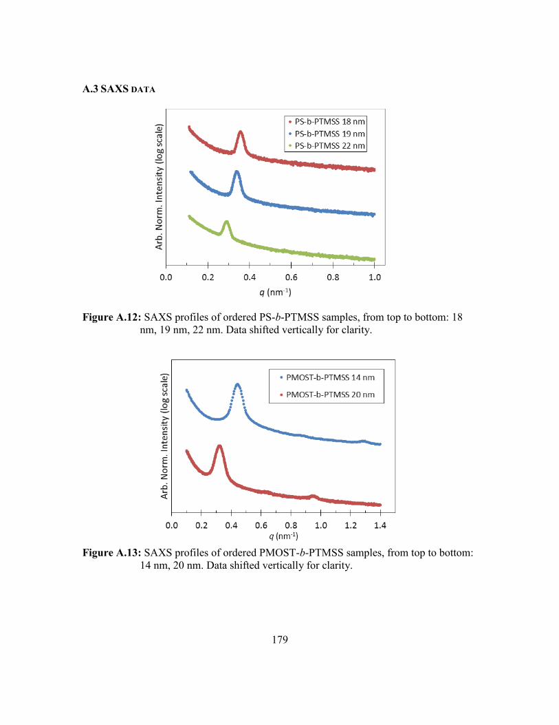
179
A.3 SAXS DATA
Figure A.12: SAXS profiles of ordered PS-b-PTMSS samples, from top to bottom: 18
nm, 19 nm, 22 nm. Data shifted vertically for clarity.
Figure A.13: SAXS profiles of ordered PMOST-b-PTMSS samples, from top to bottom:
14 nm, 20 nm. Data shifted vertically for clarity.

180
Figure A.14: SAXS profiles of ordered PMOST-b-PDSS samples, from top to bottom:
14.5 nm, 18.0 nm, 23.0 nm. Data shifted vertically for clarity.
Figure A.15: SAXS profiles of PTMSS-b-P2VP samples, from top to bottom: 10.0 nm,
10.5 nm. Data shifted vertically for clarity.

181
Figure A.16: SAXS profiles of PVBD-b-PDSS samples, from top to bottom: 8.5 nm, 9.5
nm, 10.0 nm, 10.5 nm. Data shifted vertically for clarity.
Figure A.17: SAXS profiles of PMVBD-b-PDSS samples, from top to bottom: 6.5 nm,
10.5 nm. Data shifted vertically for clarity.

182
A.4 DMS DATA
Figure A.18: DMS plots of the storage modulus (G’) of PS-b-PTMSS taken upon a
constant 5 °C/min temperature ramp. Each sample was taken at strain = 2%
and angular momentum (ω) = 1 rad/s.
Figure A.19: DMS plots of the storage modulus (G’) of PMOST-b-PTMSS and PS-b-
PDSS taken upon a constant 5 °C/min temperature ramp. Each sample was
taken at strain = 2% and angular momentum (ω) = 1 rad/s.

183
Figure A.20: DMS plots of the storage modulus (G’) and delta of PMOST-b-PDSS
(disordered sample) taken upon a constant 5 °C/min temperature ramp. The
sample was taken at strain = 2% and angular momentum (ω) = 1 rad/s. No
indication of an ODT appears in the graph, precluding the direct calculation
of χ.
Figure A.21: DMS plots of the storage modulus (G’) of PTMSS-b-P2VP taken upon a
constant 5 °C/min temperature ramp. Each sample was taken at strain = 2%
and angular momentum (ω) = 1 rad/s.

184
Figure A.22: DMS plots of the storage modulus (G’) of PVBD-b-PDSS taken upon a
constant 5 °C/min temperature ramp. Each sample was taken at strain = 2%
and angular momentum (ω) = 1 rad/s.
Figure A.23: DMS plots of the storage modulus (G’) and delta of PVBD-b-PDSS (8.5
nm disordered sample) taken upon a constant 5 °C/min temperature ramp.
The sample was taken at strain = 2% and angular momentum (ω) = 1 rad/s.
No indication of an ODT appears in the graph, precluding the direct
calculation of χ by this sample.

185
Figure A.24: DMS plots of the storage modulus (G’) of PMVBD-b-PDSS taken upon a
constant 5 °C/min temperature ramp. The sample was taken at strain = 2%
and angular momentum (ω) = 1 rad/s.

186
Appendix B: Practical considerations in anionic polymerization
Anionic polymerization is a great path to low dispersity BCPs with defined and
controlled microstructures. The BCPs introduced in this Dissertation were all synthesized
via this technique. However, anionic polymerization is not trivial to implement. The high
degree of reactivity of the carbanion propagating groups necessitates that stringent
procedures are followed to exclude any moisture or oxygen which will deleteriously
affect the polymerization, even in low amounts. In addition, there are a great number of
safety considerations when performing the polymerization that need to be addressed.
These hazards have, can, and will cause bodily harm, and knowledge about them is
necessary to mitigate danger as much as possible.
B.1 MONOMER AND SOLVENT PURIFICATION AND STORAGE
Perhaps the biggest historical hurdle to successfully conducting an anionic
polymerization was removing contaminants from the monomers. Water, oxygen, radical-
trapping inhibitors, and any other protic species will adversely affect the polymerization
by terminating reacting groups or by coupling multiple reacting groups together (while
also terminating them). The actual, hands-on procedures to perform the following
purification steps cannot be well-described in writing without necessarily omitting safety
and practical information concerning the use and manipulation of the glassware. Unless
the researcher is very experienced in air-free/water-free techniques, there is no substitute
for an apprenticeship period. However, a high-level description is provided to convey
information garnered through experience. First, generic information about handling the
purification reagents is presented, and then information about performing a successful
distillation is presented. Last, taking solvent is briefly described.

187
Oxygen and other gaseous impurities are removed by repeated freeze-pump-thaw
steps with liquid nitrogen (LN2), which exploits vapor liquid equilibrium to draw out
oxygen from the monomer. Order-of-magnitude calculations suggest that just three
freeze-pump-thaw cycles can easily reduce the oxygen partial pressure to one millionth of
the original. A freeze-pump-thaw is necessarily performed before every distillation, and
most monomer purifications have procedures involving three or more distillations,
guaranteeing at least three freeze-pump-thaw cycles. In addition, typically one to two
extra freeze-pump-thaws are performed before the first distillation, bring the number to
four or five. Last, before any freeze-pump-thaw cycles are performed, it is common
practice to open the monomer flask straight to vacuum while stirring vigorously until the
monomer just begins to boil. In this way, a bulk of the gas is removed from the monomer
without necessarily removing any significant amount of material, which improves the
effectiveness of the subsequent freeze-pump-thaw cycles. The oxygen content in the
drybox is typically 3 to 6 ppm, and it has been observed that exposing the monomer to
this degree of oxygen does not noticeably detract from the quality of the polymerization
product.
Non-gaseous impurities are removed by distilling the monomers over
organometallic bases that function as purification reagents. The purification reagents for
monomer classes are as listed in Table B.1. It is worth noting that these materials are
highly pyrophoric and require utmost care when handling AND when disposing.

188
Table B.1: Purification reagents for monomers in anionic polymerization
Monomer class Purification reagent Reference
styrene 2x di-n-butyl magnesium, 1 pipette / 10 g monomer 152
methacrylate 1x CaH2, 1 g / 5 g monomer
1x trioctylaluminum, titrated until yellow holds
54
2-vinylpyridine 1x CaH2, 1 g / 5 g monomer
1x triethylaluminum, titrated until yellow holds
152
diphenylethylene 2x n-butyl lithium, 1 pipette / 10 g monomer 54
ethylene oxide 2x butyl magnesium chloride, 1 pipette / 10 g
monomer
89
Di-n-butyl magnesium, n-butyl lithium, and butyl magnesium chloride are alike in
that these purification reagents are dispensed into Schlenk flasks with stir bars in the
drybox via a glass pipette, and then removed from the drybox (closed to the outside
environment). The solvent from these reagents only is then removed while the flask is
hooked up to a thoroughly purged manifold. Isolated di-n-butyl magnesium is a solid,
which requires a special procedure to dry fully. First, the solution is stirred as quickly as
possible and the argon in the flask is slowly bled out into the vacuum. Once the argon is
removed and a reasonably high vacuum is reached (~ 900 mtorr), the flask is opened
entirely and the solvent removed while the stirring continues. This way, the di-n-butyl
magnesium is isolated as small flakes. If the procedure is not followed, the purification
reagent may instead turn into a gel intermixed with solvent that is hard to fully dry.
Performing this part of the procedure on only one flask at a time helps prevent the
occurrence of gelling. Once dry flakes are isolated (typically seen coating the entire wall
189
of the glassware), one may open multiple flasks to the same vacuum. The flasks can be
submerged in warmed water baths (no more than 60 °C or so) to promote drying.
Typically, it may take 60 – 120 minutes to dry two such flasks. Note: n-butyl lithium and
butyl magnesium chloride are liquid when isolated, so they do not require this thorough
process.
Triethyl aluminum (TEA) and trioctyl aluminum (TOA), conversely, are not
isolated from the solution in which they are received. Instead, one distills the monomer
into an empty Schlenk flask charged with a stir bar, and then the tared flask is taken into
the glovebox where TEA or TOA are added drop-by-drop to the stirred solution until a
yellow color persists. The closed flask is then taken out of the glovebox and weighed
again. One can estimate how much of the monomer solution is now solvent (based on the
nominal concentration of the purification reagent) to accurately determine how much
monomer solution needs to be later dispensed for the reactions. The TEA- or TOA-
containing monomer is then isolated by distillation into a clean flask after approximately
one hour of stirring.
After the monomer is distilled out of the purification reagents into the final
monomer flasks, the flasks containing purification reagents should be closed while under
vacuum and disconnected from the Schlenk line. In a clear hood with no stray solvent
bottles, the neck of the flask should be filled with tetrahydrofuran (THF), and then the
plug opened just to the point that THF begins to bleed into the flask. The level of THF
should be constantly replenished while swirling the flask to make sure the sidewalls are
wetted with THF. Once one is sure the sidewalls have been wetted with THF, it is safe to
fully open the flask to air. Small amounts of isopropyl alcohol (IPA) should then be
added to the solution repeatedly and swirled. This step should be repeated with methanol
and water once one is confident that every part of the glassware has had time to react

190
with the IPA (and then the methanol). Typically, addition of only a few drops of water
causes the solution to gel. It is recommended that this mixture is poured out into the
waste as soon as possible or the flask will become hard to clean. Acetone can be used to
rinse the flask repeatedly at this point as it seems to dissolve the gel reasonably well.
Typically there will still be some visible impurities in the glassware. Soaking the flask
alternatively with THF and then dilute acid (but transitioning with acetone and water
rinses in between) usually dissolves most residues in a matter of hours. Rarely, it is
necessary to put HCl solution directly into the flask and then to let the flask sit overnight.
Label the flask as containing concentrated acid to avoid any confusion in the future.
Calcium hydride (CaH2) is the only purification reagent that does not need to be
handled inside of a drybox. The powder is poured into the Schlenk flask with a funnel,
and one needs to make sure to clean off any dust on the glass that makes contact with the
plug. Typically, CaH2 is purged 5 times with argon when connected to the vacuum, but
never flame dried. The monomer is distilled over into the CaH2 flask, and then allowed to
stir. After an adequate time interval, which can be anywhere from one hour to overnight,
the monomer is distilled, typically into an empty flask for TEA or TOA treatment.
Distilling out of CaH2 can be difficult because the powder gets carried over into the next
flask. It has been recommended that glass wool be inserted into the distillation line to
block CaH2, but this has produced mixed results as very often the glass wool is blown
into the source or destination flask via argon purges. Instead, a slow distillation is
recommended, especially of low boiling monomers like methyl methacrylate and 2-
vinylpyridine. If a visible amount of CaH2 is transferred, a second distillation is
recommended. The CaH2–containing flask does not need to be cleaned as delicately as
flasks containing the other purification reagents, but care is needed since CaH2 is still
highly reactive. In addition, it can stain glassware and build deposits which can in turn

191
prevent a high degree of vacuum from being reached when the deposits are on the glass
region that interfaces with the plug. CaH2 should be emptied into its own glass disposal
beaker using alcohol. IPA and methanol are both good at removing residual powder from
the flask. It has been found that acetone and THF causes CaH2 to form insoluble residues
and actually hamper the cleaning effort. Once all visible CaH2 is removed, these solvents
can be used. Acid, either dilute or concentrated, can again be used to deal with any
insoluble salts.
Conducting the distillation of high boiling point monomers is difficult since the
monomers begin to slowly polymerize in a hot water bath. Durand38 describes custom
glassware that maintains an open connection to the vacuum to help with this process. In
addition, Durand describes angled distillation glassware to help condense and isolate
monomer. Typically, monomers like styrene or methyl methacrylate can be distilled at a
30 – 40 °C water bath. 4-methoxystyrene requires 55 – 65 °C, while 4-
trimethylsilylstyrene needs approximately 70 °C. Monomers larger than 4-
trimethylsilylstyrene (FW 176 g/mol) need near boiling water for transfer.
Heat wrap can be used to expedite the distillation of high boiling point monomers.
Heat wrap is recommended even for 4-methoxystyrene (FW 134 g/mol), and definitely
for monomers larger than this. The heat wrap needs to be wrapped tightly around the
glass in order for the heat to transfer effectively and evenly. Of special importance is the
need to wrap the region where the plug sits in both the sending and receiving flask.
Monomer tends to pool here because the thick glassware and Teflon plug take longer to
heat than the rest of the apparatus. In addition, the tight-fitting plug can wick away liquid
monomer, further slowing down the transfer. Often this area of the glassware is neglected
due to the cramped geometry, but with practice becomes extremely easy to wrap. Once
wrapped tightly, the heat wrap needs only to be operating at 5 – 15% of total power.

192
More power and hotter temperatures have caused the polymerization of the monomer
inside the glass tubing. Often monomer will condense in the U-shaped portion of the
Schlenk line. This portion of glassware can also be wrapped with heat wrap, or it can be
warmed with a heat gun. Often, the monomer that condenses here is ignored since the
amount it is so small and the rest of the monomer continues transferring nonetheless.
Low boiling point monomers, and especially solvents, can also pose difficulties if
they transfer too quickly. If CaH2 is used, a quick transfer again propels the material into
the next flask. Even with other purification reagents, too fast of a transfer can cause the
solution to bump due to the small tubing cross-section, transferring the purification
reagent into the distillation tubing and sometimes the next flask. Ensuring adequate head
space (flasks filled no more than half way) and vigorous stirring helps to prevent this
from occurring. In addition, using a modest temperature is recommended. For solvents,
this usually means keeping the source flask in a room temperature water bath or even an
ice bath. Last, for severe problems with bumping, the angled distillation tubing can be
used in reverse to create an “uphill” path for the liquid to follow, helping to trap the
purification reagent behind in the source flask.
A common issue is not knowing when a distillation is finished and not knowing
how to efficiently transfer to the next step. Action needs to be taken when the flask looks
visibly dry, and definitely when the stir bar stops stirring. First, the plug on the sending
flask needs to be closed, and the heat wrap turned off. The LN2 in the receiving flask
should be topped off, and one should wait for approximately 3 – 5 minutes. Then, the
LN2 should be topped off again, and the heat wrap removed to inspect the glass tubing. If
liquid monomer is found, one should attempt to heat it with the heat gun to transfer it into
the receiving flask. After no more than 1 – 2 minutes of trying to recover this monomer,
or if no liquid monomer was detected, the system should be opened to vacuum and

193
allowed to achieve baseline. Any residual liquid monomer should be heated once again,
and typically within five minutes baseline is achieved. The receiving flask, which is still
open to vacuum, should be closed and thawed safely, and then the glassware should be
disassembled and reassembled as needed for the next distillation step.
When distilling into the final purification flask, the entire glass assembly,
including the U-shaped portion of the Schlenk line, needs to be flame dried with a butane
torch repeatedly. Typically, the entire assembly is flame dried three times, undergoes five
pump purges, and at least one of those pump purges is a freeze-pump-thaw of the source
flask (where the neck is also flame dried when the stop cock is opened). This is to ensure
that as much water is removed as possible. Care must be taken not to heat the metal or
rubber sections for too long. Care must also be taken to flame dry the reverse side of the
glassware as well as the front. Heat wrap, if used, should be applied during the pump
stage of the last freeze-pump-thaw cycle while both flasks are open to vacuum.
Isolated monomer should be thawed to the point where approximately half of it is
still frozen, and then the flask should be backfilled with argon and sealed at a modest
overpressure (1-3 psig). The flask of half-frozen monomer should be massed to determine
the final distillation yield and then put into the glovebox as soon as possible. Typically,
losses after three distillations amount to no more than 1 g for 4-trimethylsilylstyrene and
lighter monomers (ignoring, of course, any large issue that arise). One should anticipate
larger losses than 1 g for higher boiling-point monomers.
Once fully distilled and isolated, the monomers have a finite but unfortunately
undefined lifetime before they begin to autopolymerize and become useless for anionic
polymerization. From experience, styrene and methyl methacrylate can be stored in a
drybox freezer for at least one night before being used, but anecdotes suggest they may
have a lifetime of a week or so. Some monomers like diphenylethylene and 4-

194
methoxystyrene freeze at freezer temperatures, so they have displayed longer lifetimes
(on the order of months for diphenylethylene).
Of special note are the styrenes 4-trimethylsilylstyrene and 4-
pentamethyldisilylstyrene. These have a notably short lifetime once purified, and
typically by the next day have turned into a stringy solution believed to be an indication
of autopolymerization. These monomers are typically distilled and used on the same day
for the best polymerization products.
Compared to the involved process used to purify monomer, obtaining purified
solvent is relatively trivial. The solvent delivery system (SDS) delivers suitable solvent
straight to a flask. The flask, fitted with a plug but open, should be attached to the Cajon
fitting, subjected to vacuum, and allowed to baseline. If baseline is not readily achieved
(no more than 10 mtorr or so above the baseline achieved with all the valves closed), the
flask should be taken off the vacuum and the Cajon fitting and plug should be inspected.
Very often the rubber o-ring in the Cajon fitting on the SDS can tear due to repeated use.
Once a suitable vacuum is achieved, the entire apparatus should be pump-purged with
argon at least two times, and then flame dried with pump-purge at least three times.
Again, flame dry the neck but avoid flame drying the metal fittings. The flask should be
left under vacuum and allowed to cool before dispensing solvent. Solvent should be
dispensed only to a flask under vacuum. Drawing a line on the flask with a permanent
marker parallel to the lip of the metal ledge on which the flask sits indicates a fill level
that yields approximately 130 – 140 g of THF. Sometimes, closer to 100 g is desired,
which requires practice to approximate. Once the solvent is taken, the flask should be
filled with argon and closed, and vacuum should be enabled yet again. Inevitably, a
sizeable amount of solvent remains in the neck of the flask which needs to be removed by
vacuum to ensure a good seal in the flask. The ribbed metal piece quickly becomes very

195
cold under vacuum and can be warmed gently with the heat gun. Once baseline is
achieved with the neck of the closed flask, the SDS should be turned to argon and the
neck refilled. While under argon, the plug should be briefly opened to allow trapped THF
to travel into the flask. The flask should be closed a second time, and then evacuated one
more time. This time, typically only a tiny amount of residual solvent needs to be
removed and baseline is achieved quickly. The plug should be confirmed to be tightly
closed, and then the flask is removed. At this point, the weight of the flask should be
noted and compared with the tare weight to determine the amount of solvent received.
The flask should be stored way from light in a safe place where it will not be knocked
over.
B.2 REACTOR SETUP
Reactors should be set up to test as soon as possible since achieving vacuum
baseline is often problematic. Once solvent is acquired, the reactor can often be set up on
the same Schlenk line right away. The reactors used in the Willson and Ellison labs are
five port threaded reactors. Very often not all five ports are used, but there exists many
different combinations of glassware than can be used in conjunction with the reactor.
Typically, using Figure B.1 as a reference, port 1 has a glass blank, port 2 has the solvent
flask, port 3 should have the vacuum adaptor, port 4 has another blank, the burette
adaptor, or simply a burette, and port 5 has a thermocouple well. In this configuration, a
right-handed operator can access the valve on the solvent flask without too much trouble,
and a path to the septum on port 3 is still open. Putting the solvent on either of the front
two ports blocks access to the septum and also puts too much torque on reactor, held up
by clamps on ports 1 and 2. Putting the burette adaptor or a burette on port 5 often puts it
too close to the solvent flask in port 2, so port 4 is a better choice. A line going to vacuum
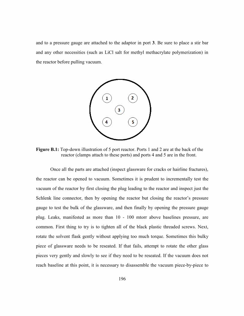
196
and to a pressure gauge are attached to the adaptor in port 3. Be sure to place a stir bar
and any other necessities (such as LiCl salt for methyl methacrylate polymerization) in
the reactor before pulling vacuum.
Figure B.1: Top-down illustration of 5 port reactor. Ports 1 and 2 are at the back of the
reactor (clamps attach to these ports) and ports 4 and 5 are in the front.
Once all the parts are attached (inspect glassware for cracks or hairline fractures),
the reactor can be opened to vacuum. Sometimes it is prudent to incrementally test the
vacuum of the reactor by first closing the plug leading to the reactor and inspect just the
Schlenk line connector, then by opening the reactor but closing the reactor’s pressure
gauge to test the bulk of the glassware, and then finally by opening the pressure gauge
plug. Leaks, manifested as more than 10 - 100 mtorr above baselines pressure, are
common. First thing to try is to tighten all of the black plastic threaded screws. Next,
rotate the solvent flask gently without applying too much torque. Sometimes this bulky
piece of glassware needs to be reseated. If that fails, attempt to rotate the other glass
pieces very gently and slowly to see if they need to be reseated. If the vacuum does not
reach baseline at this point, it is necessary to disassemble the vacuum piece-by-piece to

197
determine the culprit. Often, very short, stubby tubing, either on the blanks or on the
vacuum adaptor, causes an insufficient seal to form. The glassware should be replaced
with some with longer tubing. In addition, the white Teflon ferrule fittings sometimes
need to be replaced. Anecdotally, it seems that ferrule fittings that initially sit much
looser on their glass tubing make better connections. Fittings that are initially tight
should be replaced with looser fittings.
B.3 CONDUCTING A POLYMERIZATION
With a reactor that achieves baseline, it is possible to proceed with the actual
polymerization. The reactor should be pump-purged at least two times, and then flame
dried with pump-purging at least three times. The glassware, including the vacuum
adaptor and the Schlenk line, should be flame dried as well. Care should be taken not to
heat any plastic, metal, or rubber portion for too long.
B.3.1 Cooling the reactor
Once a satisfactory flame dry is performed, the reactor should be allowed to cool
under vacuum, and then filled with argon to approximately two psig. The plug to the
reactor should be closed, but the Schlenk line should be left open to argon. The solvent
flask should then be opened and the solvent allowed to flow into the reactor. Screw the
plug closed once the solvent has emptied into the reactor. Stirring should now commence.
Now the reactor should be cooled with LN2 while monitoring the temperature with a
thermocouple. The Dewer containing LN2 may be lifted up closer to the reactor to
submerge more of the reactor in the LN2 to speed up the cooling. While the reactor is
cooling the pressure in the reactor also needs to be monitored. The reactor should be
refilled repeatedly with argon at this point to three psig, and never allowed to reach
below one psig. One needs to be alert since there is a delay between the temperature of

198
the bottom of the solvent and the temperature of the solvent in the thermocouple well.
The solvent may get too cold and freeze- the target temperature is -78 °C but the freezing
point of THF is -108 °C. Typically, it takes approximately two dewer refills of LN2 to
reach this temperature for a 500 mL reactor flask. If the solvent is kept stirring, it should
be fine even if part of it freezes. At approximately -75 to -85 °C, IPA and crushed dry ice
should be added to the LN2 flask. Any residual LN2 will quickly evaporate. If the solvent
had ceased stirring due to freezing, it should also be warmed with IPA and dry ice after
pouring out the excess LN2.
Once the reactor is submerged with IPA, the Schlenk line needs to be switched
from argon to vacuum and the pressure monitored again. The slow warming of the
reactor to -78 °C will increase the pressure. This should be countered by slowly bleeding
off pressure by slightly opening up the port to the reactor. This becomes much more
important if the solvent froze, since the temperature may change abruptly. Constantly
refill the dry ice in the IPA and stir the slurry to maintain even cooling. Once the pressure
and temperature of the reactor has equilibrated (in practice around -72 °C), the initiator
can be added.
B.3.2 Dispensing the initiator
The preferred initiator for anionic polymerization is sec-butyllithium (sBuLi) 1.4
M in cyclohexane from Sigma-Aldrich. It is worth repeating that this organometallic is
extremely pyrophoric and that a related compound was the cause of the death of a
researcher a few years back. Only dispense the compound in the glovebox with a glass,
gas-tight syringe.
Before operating the glovebox, fill two 50 mL beakers halfway with THF and set
them near the reactor. These will be used to quench and purge the sBuLi syringe.

199
Deliberately decide which beaker to take from and which beaker to purge into. Clear out
space near the reactor to remove clutter. Solvent bottles should be removed as well.
In the glovebox, the sBuLi is drawn out. A good idea is to remove the sBuLi from
the glovebox freezer right before dispensing the THF into the reactor to allow the sBuLi
time to warm up. Typically, an amount of sBuLi solution is brought into the syringe and
then the plunger is moved to about 10% of the syringe’s capacity further than the desired
amount. The syringe is then held upside down, with the needle point up, while the
plunger is pushed closed against the glovebox shelf. This removes any gas in the syringe
and also wets the syringe barrel with sBuLi, cleaning it in the process. The drawback is
that impurities concentrate in the sBuLi. (Because of this, small 25 mL bottles are
recommended for use despite costing a nominal premium.) The desired amount of sBuLi
is then taken up, and the needle is immediately removed from the glovebox and taken to
the reactor(s). As a rule of thumb, for safety the syringe should not be not filled more
than halfway.
Before inserting the needle into the reactor, one droplet of sBuLi is typically
dropped onto the fume hood countertop to “clean” the needle tip of any residue. The
importance of this practice is unsubstantiated but followed nonetheless. The needle is
immediately inserted into the reactor and the syringe and needle apparatus is arranged so
that one can easily see the graduations on the barrel. The sBuLi is dispensed into the
reactor, forming a characteristic neon yellow color. After all the reactors are initiated
with sBuLi, THF from one of the beakers is drawn up into the syringe and mixed with
any residual sBuLi solution before being purged into the second beaker with the needle
below the THF level. This is repeated five times to clean the syringe and ensure no sBuLi
remains in the syringe. The reactor(s) with sBuLi is(are) allowed to stir for approximately
one hour, the time it takes for the glovebox to be prepared for monomers.

200
It is prudent to take more sBuLi than anticipated since inevitably some portion of
the sBuLi will “die” to residual impurities in the THF, and additional sBuLi needs be
delivered to the reactor to compensate for this loss. There are two ways to determine how
much extra sBuLi is needed. The color of the reaction should be monitored as the sBuLi
is added drop-by-drop to the reactor. At some point, the characteristic yellow color
develops. The plunger position at this point in time should be noted. At the point that the
color begins to hold, regardless of how much liquid actually entered the reactor,
experience shows that the reactor has received an effective “dose” of 0.2 to 0.6 mL of the
1.4 M sBuLi. The remainder that is necessary should be estimated based on the goals of
the polymerization and calculated from the plunger position. The total amount of liquid
dispensed and the point at which color first held are typically noted. These values can be
used in the second procedure, known as “dead fraction calculation”. Essentially, simply
from the amount of sBuLi dispensed into the reactor, the molecular weight of the product
polymer as determined by some technique like MALDI, and the amount of monomer
used in the reaction, the number of sBuLi molecules that “sprouted” into chains can be
calculated “posthumously”, which can be used then to calculate how many milliliters of
1.4 M sBuLi “died” due to solvent. This value typically scales with amount of solvent
dispensed into the reactor, and ranges from 0.04 to 0.15 mL / 100 g THF. This value may
change from reaction to reaction, but is still tracked to inform subsequent polymerization
attempts.
B.3.3 Dispensing monomer
The historical way to dispense monomer into threaded-port reactors was to use a
graduated burette. However, this method fell out of favor while working with the high-χ,
silicon-containing BCPs for a number of reasons. First, the purification procedure is

201
slower since multiple burettes need to be filled one by one if running multiple reactions.
Second, when working with the silicon-containing monomers, the relatively small
amount of the non-commercially available monomer used (~5 g of each monomer for ~10
g total) became difficult to accurately measure out from the burette into the reactor.
However, using a burette works and is recommended once one starts manipulating ~20 g
of monomer or more at a time.
The more convenient way found to dispense the monomer, especially at the scale
at which we are operating, is to use a plastic syringe. Specifically, the ubiquitous Luer
Lock Norm-Ject® plastic syringes by Henke Sass Wolf (Germany), coupled to a standard
stainless steel needle, are able to hold a sufficient seal that the monomer can be removed
from the drybox and injected into the reactor and form essentially flawless BCPs. The
graduations printed on the syringes are sufficient to withdraw and deliver monomer
accurately. The nominally 5 mL (and smaller) syringes are especially convenient since
the barrel of the syringe fits into the glass neck of a standard Schlenk flask, permitting
one to insert even a relatively short needle (~20 cm) very far into the flask. The
nominally 10 mL syringes are unfortunately too thick to fit into the neck of the flask.
These require a standard 30 cm steel needle to adequately draw up monomer. The length
of the needle becomes important because the drybox antechamber can only fit a certain
length of apparatus. A fully withdrawn 10 mL syringe will require the corresponding 30
cm needle to be bent to a large degree. This strains the Luer joint significantly and is
anticipated to be a point of failure for at least one reaction. A fully withdrawn 5 mL
syringe with a 20 cm needle or a 10 mL syringe withdrawn to approximately 8 mL with a
30 cm needle fit comfortably in the glovebox antechamber.
Before inserting into the reactor, one droplet of monomer is dropped outside the
reactor (usually directly on the wall of the reactor) and then the needle is inserted

202
immediately after. Just like with the sBuLi, this practice is believed to help keep the
needle tip clean.
The needle should be positioned in such a way that the monomer flows directly
into the THF vortex. Monomer that splashes onto the side of the reactor creates pockets
of high monomer concentration and has led to the formation of gels on the glass wall.
The monomer should be added drop-by-drop, with an eye on the temperature of the
reactor. Typically, the addition of most styrenes can warm the reactor to approximately
negative 60 °C without causing evidence of chain termination to occur, but it is
anticipated that this value is too warm for the silated-styrenes and acrylic and methacrylic
monomers, and negative 65 °C is a more conservative target.
It is also possible to use glass air-tight syringes to dispense monomer. However,
they need to be cleaned thoroughly between uses because small but not insignificant
amounts of monomer adhere to their Luer lock assemblies. Multiple reactions have been
contaminated with monomer from previous reactions despite a relatively thorough degree
of cleaning occurring in-between. In this regard, the cheap, disposable plastic syringes
are preferred.
B.3.4 Taking an aliquot
After the first monomer is inserted, an aliquot needs to be taken to analyze the
first block of the BCP. Typically, the monomer is allowed to react for approximately one
hour for styrenes (but longer for diphenylethylene or methyl methacrylate). During this
time, methanol is degassed via argon from the Schlenk line in a 125 mL Erlenmeyer flask
sealed with a septum. Also during this time, needles without warped tips and without
signs of rust should be identified, cleaned, and put in the drying oven. The line running to
the reactor should be under vacuum for all reactors (but the plug still closed).
203
To take an aliquot, the methanol purge first needs to be stopped. While
maintaining the flow of argon, the purging needle is raised out of the methanol (but kept
in the flask), then the vent needle is moved, and then immediately after that the purging
needle is removed. The argon flow to that needle should now be turned off. Repeat for all
methanol Erlenmeyer flasks.
Next, one needle is removed from the drying oven and taken to a reactor. That
reactor’s line is switched from vacuum to argon. The plug to the reactor is opened, and
then the hot needle is inserted immediately through the septum but not into the THF (aim
to insert at least 10 – 15 cm of the hot needle into the reactor). Argon is allowed to flow
through the needle. Once the needle has cooled down (~30 s), a plastic 5 mL Luer
locking plastic syringe with its plunger removed is attached to the needle. The plunger is
then pressed against the barrel opening without re-inserting the plunger fully into the
barrel. The syringe and the face of the plunger are allowed to be purged with argon for
approximately one minute. Then, the plunger is inserted all the way to the bottom of the
barrel, and held in place with a thumb. The pressure in the reactor is allowed to rise to 3
psig, and then the plug to the reactor is closed. The needle is then submerged into the
THF, and an aliquot of approximately 3 mL is drawn up. After a sufficient amount of
liquid is drawn up, the needle is lifted out of the THF and argon is drawn into the syringe
to clear out the needle and prevent spillback of the solution into the reactor’s THF. The
needle and syringe, now very cold, are quickly removed from the reactor and inserted
immediately through the septum of the methanol flask, then the needle tip is inserted
below the level of the methanol, and the syringe contents are quickly pushed out. A white
precipitate forms. Some color may persist in the syringe, indicating living anion. The
syringe should be quenched with THF before being thrown out.

204
The procedure is repeated with each reactor. Keep in mind that now there is argon
in each line. The pressure in each reactor should be adjusted to maintain 3 psig, and the
lines switched to vacuum after isolating the reactors from each line.
After the aliquot is taken, the second monomer is typically dispensed in the same
way as the first. If only one monomer is being used, an aliquot is typically not taken.
Care must be taken during the aliquot taking process because every aliquot
inevitably terminates some portion of the anion in the reactor. As Figure A.7 shows,
these dead homopolymer from the aliquots are visible in the MALDI of the BCP powder
(of course, MALDI is more sensitive to low molecular weight materials). Figure A.7 is
especially unique because the three PS-b-PTMSS polymers featured in this figure were
made by taking two aliquots (and building two “blocks” of PS) to accurately hit a
molecular weight target, so both aliquots are seen in the MALDI. The other MALDI
spectrum (Figure A.8, for example) show only one aliquot since only one was taken.
B.3.5 Terminating the reaction
To terminate the reactions, a new, clean Erlenmeyer flask of methanol is purged
with argon. The needle that is going to be used to inject the methanol can be used as the
vent needle for this operation (but not for the aliquots- those needles should be dried in
the oven up until use). When sufficient time has elapsed (~ 45 minutes), a new 5 mL Luer
locking plastic syringe with its plunger removed is attached to the needle, and the plunger
is pressed up against the barrel without being inserted. The argon is again allowed to
purge the syringe for one minute, before the plunger is fully inserted, the argon turned
off, the needle dropped below the level of the methanol, and approximately 3 mL of
methanol is removed. The methanol is injected into each reactor one-by-one without too
much focus on procedure. Typically only one milliliter is needed to terminate a reaction,

205
but the color should be monitored during the termination process. Sometimes, a gradient
of color develops that indicates inefficient mixing that should be rectified in future
polymerizations. After the color disappears, the reaction is allowed to stir for five more
minutes before the argon the reactor is disconnected from vacuum and the plug opened to
vent pressure.
B.4 SAFETY
Of course, these procedures should only be conducted in the safest ways possible.
The various risks associated with the procedures are discussed below.
The biggest risk with these procedures is warming the distillation flasks after they
have been cooled to LN2 temperatures. At LN2 temperatures, argon and oxygen can
condense into liquid. Once the flask is warmed, the liquid evaporates and increases the
pressure in the flask by many orders of magnitude, potentially shattering the glass.
Glassware fitted with pressure-release valves should be used at all times to help prevent
catastrophic glass failure. In addition, one needs to be conscious of whether or not a flask
is open to vacuum. A flask should only be thawed immediately after being shut off from
the vacuum. A flask that has not been subjected to vacuum should not be thawed. The
Schlenk line valve and the plug on the flask should be confirmed to be open before
assessing whether or not a sufficient vacuum has been achieved to allow for safe thawing.
In addition, monomers such as ethylene oxide or isoprene pose specific dangers
since there are mechanisms by which the pressure in the purification flasks may rise to a
dangerous level without being cooled by LN2. The temperature of the solutions of both
monomers needs to be maintained at or below ice water temperature. Ethylene oxide
boils at only 10 °C, so care must be taken to keep this monomer a liquid. In addition,
ethylene oxide may be highly contaminated, which can cause the pressure in at least the

206
first purification flask to increase substantially. It may be prudent to bleed off some of the
pressure while thawing to prevent pressure buildup. Isoprene has been ignored by the
author since it is not a material he has worked with, but bears mention here since multiple
accidents have been caused by this material. At elevated temperatures, isoprene reacts
with its purification reagent to polymerize and generates a substantial amount of heat.
Isoprene’s boiling point is only 34 °C, which may be quickly reached by a runaway
reaction, leading to a surprising buildup of pressure and broken glassware. Again, both of
these monomers, and similar compounds, need to be kept at or below ice water
temperature at all times. It is not recommended that one ever try to work with these
materials without hands-on training from an expert, regardless of their proficiency with
other anionic polymerization materials.
In the same vein, all purification reagents may produce gaseous materials as by-
products of the purification process. This is especially significant for CaH2 which may
produce H2 gas. When the monomer is first thawed and allowed to react with the
purification reagent, any large degree of bubbling should be noted since this might
indicate a release of gaseous by-products. These should be bled out into the vacuum. If
one goes to freeze-pump-thaw the purification flask before distillation and the pressure
reaches > 400 mtorr before baselining, it is recommended that a second freeze-pump-
thaw be performed to remove any additional volatile by-products. Of course, these
purification reagents should only be used in flasks with pressure release valves.
The cryogens used to cool the reactor (dry ice) and cool the vacuum trap and
purification flasks (LN2) also need to be treated with care. Use personal protective
equipment (PPE) in the form of gloves to avoid prolonged contact with these materials.
Be cautious when filling up the vacuum trap since LN2 may pool in the cuff of a lab coat
while pouring and cause burns on the wrist.
207
LN2 poses another specific threat. Oxygen may condense in the vacuum trap if
too much air is continuously pulled into the vacuum line. Liquid oxygen reacts violently
with any organic compounds, such as those that may also be condensed in the vacuum
trap. Do not run the vacuum continuously open to oxygen (for example, in a traditional
distillation) with an LN2 trap. Use a dry ice trap instead.
The butane torch used to flame dry the glassware can also pose a risk. Do not
flame dry with solvent bottles (plastic or glass) in the hood. Metal tins now exist in each
fume hood to conveniently move all the solvent bottles at once out of the hood. Glass
solvent bottles, typically used for waste, should also be removed. Metal fittings, rubber,
and plastic should not be flame dried. Use the flame-resistant lab coats provided by the
department at all times.
And last, as already mentioned, the purification reagents and initiator are highly
pyrophoric organometallics. Practices must be maintained to exclude air and water from
these materials. Sigma-Aldrich publishes an online safety training that discusses the safe
handling of pyrophoric materials.

208
References
(1) ENIAC: Celebrating Penn Engineering History http://www.seas.upenn.edu/about-
seas/eniac/operation.php.
(2) Campbell, S. A. Fabrication Engineering at the Micro- and Nanoscale; 3rd
Editio.; Oxford University Press: New York, New York, 2008.
(3) Moore, G. E. Cramming More Components onto Integrated Circuits. IEEE Solid-
State Circuits Soc. Newsl. 2006, 20, 33–35.
(4) Shimpi, A. L. Intel Announces first 22nm 3D Tri-Gate Transistors, Shipping in 2H
2011 http://maltiel-consulting.com/Intel_22nm_3D_Tri-
Gate_FinFETs_Transistors_maltiel_semiconductor_consulting.html.
(5) Bruning, J. H. Optical Lithography: 40 Years and Holding. Proc. SPIE 2007,
6520, 652004 1–13.
(6) Willson, C. G.; Dammel, R. A.; Reiser, A. Photoresist Materials: A Historical
Perspective. Proc. SPIE 1997, 3051, 28–41.
(7) Levenson, M. D.; Viswanathan, N. S.; Simpson, R. a. Improving Resolution in
Photolithography with a Phase-Shifting Mask. IEEE Trans. Electron Devices
1982, 29, 1828–1836.
(8) Pease, R. F.; Chou, S. Y. Lithography and Other Patterning Techniques for Future
Electronics. Proc. IEEE 2008, 96, 248–270.
(9) Johnson, S. C.; Bailey, T. C.; Dickey, M. D.; Smith, B. J.; Kim, E. K.; Jamieson,
A. T.; Stacey, N. A.; Ekerdt, J. G.; Willson, C. G. Advances in Step and Flash
Imprint Lithography. Proc. SPIE 2003, 5037, 197–202.
(10) Hua, F.; Sun, Y.; Gaur, A.; Meitl, M. A.; Bilhaut, L.; Rotkina, L.; Wang, J.; Geil,
P.; Shim, M.; Rogers, J. A. Polymer Imprint Lithography with Molecular-Scale
Resolution. Nano Lett. 2004, 4, 2467–2471.
(11) Ye, Z.; Carden, S.; Hellebrekers, P.; LaBrake, D.; Resnick, D. J.; Melliar-Smith,
M.; Sreenivasan, S. V. Imprint Process Performance for Patterned Media at
Densities Greater than 1Tb/in2. Proc. SPIE 2012, 8323, 83230V 1–6.
(12) Arnold, W. H. Double-Patterning Lithography. J. Micro/Nanolithography, MEMS,
MOEMS 2009, 8, 011001–1.
(13) Abercrombie, D. Self-Aligned Double Patterning - Part Deux
http://semiengineering.com/self-aligned-double-patterning-part-deux/.
(14) Hori, M.; Nagai, T.; Nakamura, A.; Abe, T.; Wakamatsu, G.; Kakizawa, T.; Anno,
Y.; Sugiura, M.; Kusumoto, S.; Yamaguchi, Y.; et al. Sub-40nm Half-Pitch
Double Patterning with Resist Freezing Process. Proc. SPIE 2008, 6923, 69230H
1–8.

209
(15) Ando, T.; Takeshita, M.; Takasu, R.; Yoshii, Y.; Iwashita, J.; Matsumaru, S.; Abe,
S.; Iwai, T. Pattern Freezing Process Free Litho-Litho-Etch Double Patterning.
Jpn. J. Appl. Phys. 2009, 48, 06FC01 1–20.
(16) Chen, Y.; Cheng, Q.; Kang, W. Technological Merits, Process Complexity, and
Cost Analysis of Self-Aligned Multiple Patterning. Proc. SPIE 2012, 8326,
832620 1–14.
(17) Gargini, P. ITRS Past, Present and Future
https://www.dropbox.com/s/6eskh6bwdcuzpsa/1507_11_Paolo
Overview_Out.pdf?dl=0.
(18) ITRS 2013 Executive Summary http://www.itrs2.net/itrs-reports.html (accessed
Jun 4, 2016).
(19) Leibler, L. Theory of Microphase Separation in Block Copolymers.
Macromolecules 1980, 1617, 1602–1617.
(20) Bates, F. S.; Fredrickson, G. H. Block Copolymer Thermodynamics: Theory and
Experiment. Annu. Rev. Phys. Chem. 1990, 41, 525–557.
(21) Matsen, M. W. The Standard Gaussian Model for Block Copolymer Melts. J.
Phys. Condens. Matter 2002, 14, R21–R47.
(22) Matsen, M. W.; Bates, F. S. Unifying Weak-and Strong-Segregation Block
Copolymer Theories. Macromolecules 1996, 29, 1091–1098.
(23) Sinturel, C.; Bates, F. S.; Hillmyer, M. A. High χ–Low N Block Polymers: How
Far Can We Go? ACS Macro Lett. 2015, 4, 1044–1050.
(24) Stoykovich, M. P.; Nealey, P. F. Block Copolymers and Conventional
Lithography. Mater. Today 2006, 9, 20–29.
(25) Chang, J.-B.; Son, J. G.; Hannon, A. F.; Alexander-Katz, A.; Ross, C. a; Berggren,
K. K. Aligned Sub-10-Nm Block Copolymer Patterns Templated by Post Arrays.
ACS Nano 2012, 6, 2071–2077.
(26) Black, C. T.; Ruiz, R.; Breyta, G.; Cheng, J.; Coulborn, M.; Guarini, K.; Kim, H.;
Zhang, Y. Polymer Self-Assembly in Semiconductor Microelectronics. IBM J.
Res. Dev 2007, 51, 605–633.
(27) Doise, J.; Bekaert, J.; Chan, B. T.; Gronheid, R.; Cao, Y.; Hong, S.; Lin, G.;
Fishman, D.; Chakk, Y.; Marzook, T. Implementation of Surface Energy
Modification in Graphoepitaxy Directed Self-Assembly for Hole Multiplication. J.
Vac. Sci. Technol. B, Nanotechnol. Microelectron. Mater. Process. Meas. Phenom.
2015, 33, 06F301 1–9.
(28) Sinturel, C.; Vayer, M.; Morris, M.; Hillmyer, M. A. Solvent Vapor Annealing of
Block Polymer Thin Films. Macromolecules 2013, 46, 5399–5415.
(29) Pathangi, H.; Stokhof, M.; Knaepen, W.; Vaid, V.; Mallik, A.; Chan, B. T.;

210
Vandenbroeck, N.; Maes, J. W.; Gronheid, R. Improved Cost-Effectiveness of the
Block Co-Polymer Anneal Process for DSA. Proc. SPIE 2016, 9777, 97771Z1–
Z5.
(30) Darling, S. B. Directing the Self-Assembly of Block Copolymers. Prog. Polym.
Sci. 2007, 32, 1152–1204.
(31) Rincon Delgadillo, P.; Harukawa, R.; Suri, M.; Durant, S.; Cross, A.; Nagaswami,
V. R.; Van Den Heuvel, D.; Gronheid, R.; Nealey, P. Defect Source Analysis of
Directed Self-Assembly Process (DSA of DSA). Proc. SPIE 2013, 8680, 86800L.
(32) Sayan, S.; Chan, B. T.; Marzook, T.; Vandenbroeck, N.; Sanchez, E. A.; Gronheid,
R.; Singh, A.; Rincon-Delgadillo, P. A. Directed Self-Assembly Process
Integration - Fin Patterning Approaches and Challenges. SPIE Adv. Lithogr. 2015,
9425, 94250R 1–12.
(33) Lei, W.; Ruiz, R.; Gao, H.; Patel, K. C.; Albrecht, T. R.; Yin, J.; Kim, J.; Cao, Y.;
Lin, G. The Limits of Lamellae-Forming PS-B-PMMA Block Copolymers for
Lithography. ACS Nano 2015, 9, 7506–7514.
(34) Hartney, M. A.; Chiang, J. N.; Hess, D. W.; Soane, D. S. Oxide Formation during
Plasma Etching of Silicon-Containing Resists. Appl. Phys. Lett. 1989, 54, 1510.
(35) Azarnouche, L.; Sirard, S. M.; Durand, W. J.; Blachut, G.; Gurer, E.; Hymes, D. J.;
Ellison, C. J.; Willson, C. G.; Graves, D. B. Plasma and Photon Interactions with
Organosilicon Polymers for Directed Self-Assembly Patterning Applications. J.
Vac. Sci. Technol. B Microelectron. Nanom. Struct. 2016, 34, 061602 1–10.
(36) Bates, C. M. Advanced Materials for Block Copolymer Lithography, University of
Texas, Austin, 2013.
(37) Maher, M. J. Next Generation Materials for Block Copolymer Lithography,
University of Texas, Austin, 2016.
(38) Durand, W. J. Design, Synthesis, and Engineering of Advanced Materials for
Block Copolymer Lithography, University of Texas, Austin, 2015.
(39) Maher, M. J.; Bates, C. M.; Blachut, G.; Sirard, S.; Self, J. L.; Carlson, M. C.;
Dean, L. M.; Cushen, J. D.; Durand, W. J.; Hayes, C. O.; et al. Interfacial Design
for Block Copolymer Thin Films. Chem. Mater. 2014, 26, 1471–1479.
(40) Durand, W. J.; Blachut, G.; Maher, M. J.; Sirard, S.; Tein, S.; Carlson, M. C.;
Asano, Y.; Zhou, S. X.; Lane, A. P.; Bates, C. M.; et al. Design of High-χ Block
Copolymers for Lithography. J. Polym. Sci. Part A Polym. Chem. 2015, 53, 344–
352.
(41) Maher, M. J.; Bates, C. M.; Blachut, G.; Carlson, M. C.; Self, J. L.; Janes, D. W.;
Durand, W. J.; Lane, A. P.; Ellison, C. J.; Willson, C. G. Photopatternable
Interfaces for Block Copolymer Lithography. ACS Macro Lett. 2014, 3, 824–828.

211
(42) Turner, M. S. Equilibrium Properties of a Diblock Copolymer Lamellar Phase
Confined between Flat Plates. Phys. Rev. Lett. 1992, 69, 1788–1791.
(43) Walton, D. G.; Kellogg, G. J.; Mayes, A. M.; Lambooy, P.; Russell, T. P. A Free
Energy Model for Confined Diblock Copolymers. Macromolecules 1994, 27,
6225–6228.
(44) Peters, R. D.; Yang, X. M.; Kim, T. K.; Sohn, B. H.; Nealey, P. F. Using Self-
Assembled Monolayers Exposed to X-Rays To Control the Wetting Behavior of
Thin Films of Diblock Copolymers. Langmuir 2000, 16, 4625–4631.
(45) Shelton, C. K.; Epps, T. H. Decoupling Substrate Surface Interactions in Block
Polymer Thin Film Self-Assembly. Macromolecules 2015, 48, 4572–4580.
(46) Mansky, P.; Liu, Y.; Huang, E.; Russell, T. P. Controlling Polymer-Surface
Interactions with Random Copolymer Brushes. Science (80-. ). 1997, 275, 1458–
1460.
(47) Ji, S.; Liu, C.-C.; Son, J. G.; Gotrik, K.; Craig, G. S. W.; Gopalan, P.; Himpsel, F.
J.; Char, K.; Nealey, P. F. Generalization of the Use of Random Copolymers To
Control the Wetting Behavior of Block Copolymer Films. Macromolecules 2008,
41, 9098–9103.
(48) Bates, C. M.; Strahan, J. R.; Santos, L. J.; Mueller, B. K.; Bamgbade, B. O.; Lee, J.
a; Katzenstein, J. M.; Ellison, C. J.; Willson, C. G. Polymeric Cross-Linked
Surface Treatments for Controlling Block Copolymer Orientation in Thin Films.
Langmuir 2011, 27, 2000–2006.
(49) Keen, I.; Yu, A.; Cheng, H.; Jack, K.; Nicholson, T. M.; Whittaker, A. K.; Blakey,
I. Control of the Orientation of Symmetric Poly(styrene)-Block-Poly(d,l-Lactide)
Block Copolymers Using Statistical Copolymers of Dissimilar Composition.
Langmuir 2012, 28, 15876–15888.
(50) Bates, C. M.; Seshimo, T.; Maher, M. J.; Durand, W. J.; Cushen, J. D.; Dean, L.
M.; Blachut, G.; Ellison, C. J.; Willson, C. G. Polarity-Switching Top Coats
Enable Orientation of Sub-10-Nm Block Copolymer Domains. Science (80-. ).
2012, 338, 775–779.
(51) Bang, J.; Bae, J.; Löwenhielm, P.; Spiessberger, C.; Given-Beck, S. a.; Russell, T.
P.; Hawker, C. J. Facile Routes to Patterned Surface Neutralization Layers for
Block Copolymer Lithography. Adv. Mater. 2007, 19, 4552–4557.
(52) Ryu, D. Y.; Shin, K.; Drockenmuller, E.; Hawker, C. J.; Russel, T. P. A
Generalized Approach to the Modifiction of Solid Surfaces. Science (80-. ). 2004,
308, 236–238.
(53) Hayes, C. O.; Chen, P. H.; Thedford, R. P.; Ellison, C. J.; Dong, G.; Willson, C. G.
Effect of Ring Functionalization on the Reaction Temperature of
Benzocyclobutene Thermoset Polymers. Macromolecules 2016, 49, 3706–3715.

212
(54) Kennemur, J. G.; Hillmyer, M. a.; Bates, F. S. Synthesis, Thermodynamics, and
Dynamics of Poly(4- Tert -Butylstyrene- B -Methyl Methacrylate).
Macromolecules 2012, 45, 7228–7236.
(55) Han, E.; Leolukman, M.; Kim, M.; Gopalan, P. Resist Free Patterning of
Nonpreferential Buffer Layers for Block Copolymer Lithography. ACS Nano
2010, 4, 6527–6534.
(56) Han, E.; Stuen, K. O.; La, Y.-H.; Nealey, P. F.; Gopalan, P. Effect of Composition
of Substrate-Modifying Random Copolymers on the Orientation of Symmetric and
Asymmetric Diblock Copolymer Domains. Macromolecules 2008, 41, 9090–9097.
(57) Liu, C.-C.; Han, E.; Onses, M. S.; Thode, C. J.; Ji, S.; Gopalan, P.; Nealey, P. F.
Fabrication of Lithographically Defined Chemically Patterned Polymer Brushes
and Mats. Macromolecules 2011, 44, 1876–1885.
(58) Sparnacci, K.; Antonioli, D.; Gianotti, V.; Laus, M.; Ferrarese Lupi, F.;
Giammaria, T. J.; Seguini, G.; Perego, M. Ultrathin Random Copolymer-Grafted
Layers for Block Copolymer Self-Assembly. ACS Appl. Mater. Interfaces 2015, 7,
10944–10951.
(59) Liu, C. C.; Hernandez, A. B.; Yoshida, H.; Gopalan, P.; de Pablo, J. J.; Nealey, P.
F. Chemical Patterns for Directed Self-Assembly of Lamellae-Forming Block
Copolymers with Density Multiplication of Features. Macromolecules 2013, 46,
1415–1424.
(60) Georges, M. K.; Veregin, R. P. N.; Kazmaier, P. M.; Hamer, G. K. Narrow
Molecular Weight Resins by a Free-Radical Polymerization Process.
Macromolecules 1993, 26, 2987–2988.
(61) Hawker, C. J.; Barclay, G. G.; Orellana, A.; Dao, J.; Devonport, W. Initiating
Systems for Nitroxide-Mediated “Living” Free Radical Polymerizations :
Synthesis and Evaluation. Macromolecules 1996, 29, 5245–5254.
(62) Coulon, G.; Collin, B.; Ausserre, D.; Chatenay, D.; Russell, T. P. Islands and
Holes on the Free Surface of Thin Diblock Copolymer Films. I. Characteristics of
Formation and Growth. J. Phys. 1990, 51, 2801–2811.
(63) Kim, S.; Bates, C.; Thio, A.; Cushen, J.; Ellison, C. J.; Willson, C. G.; Bates, F. S.
Consequences of Surface Neutralization in Diblock Copolymer Thin Films. ACS
Nano 2013, 7, 9905–9919.
(64) Mansky, P.; Russell, T. P. Free-Surface Confinement of Diblock Copolymer
Multilayers. Macromolecules 1995, 28, 8092–8095.
(65) Durand, W. J.; Carlson, M. C.; Maher, M. J.; Blachut, G.; Santos, L. J.; Tein, S.;
Ganesan, V.; Ellison, C. J.; Willson, C. G. Experimental and Modeling Study of
Domain Orientation in Confined Block Copolymer Thin Films. Macromolecules
2015, 49, 308–316.

213
(66) Mahadevapuram, N.; Mitra, I.; Bozhchenko, A.; Strzalka, J.; Stein, G. E. In-Plane
and out-of-Plane Defectivity in Thin Films of Lamellar Block Copolymers. J.
Polym. Sci. Part B Polym. Phys. 2015, 54, 339–352.
(67) Liu, G.; Nealey, P. F.; Ruiz, R.; Dobisz, E.; Patel, K. C.; Albrecht, T. R.
Fabrication of Chevron Patterns for Patterned Media with Block Copolymer
Directed Assembly. J. Vac. Sci. Technol. B Microelectron. Nanom. Struct. 2011,
29, 06F204.
(68) Ruiz, R.; Dobisz, E.; Albrecht, T. R. Rectangular Patterns Using Block Copolymer
Directed Self Assembly for High Bit Aspect Ratio Patterned Media. ACS Nano
2011, 5, 79–84.
(69) Gronheid, R.; Rincon Delgadillo, P. A.; Younkin, T.; Pollentier, I.; Somervell, M.;
Hooge, J. S.; Nafus, K.; Nealey, P. F. Frequency Multiplication of Lamellar Phase
Block Copolymers with Grapho-Epitaxy Directed Self-Assembly Sensitivity to
Prepattern. J. Micro/Nanolithography, MEMS, MOEMS 2012, 11, 031303.
(70) Somervell, M.; Gronheid, R.; Hooge, J.; Nafus, K.; Rincon Delgadillo, P.; Thode,
C.; Younkin, T.; Matsunaga, K.; Rathsack, B.; Scheer, S.; et al. Comparison of
Directed Self-Assembly Integrations. Proc. SPIE 2012, 8325, 83250G.
(71) Ting, Y.-H.; Park, S.-M.; Liu, C.-C.; Liu, X.; Himpsel, F. J.; Nealey, P. F.; Wendt,
A. E. Plasma Etch Removal of Poly(methyl Methacrylate) in Block Copolymer
Lithography. J. Vac. Sci. Technol. B Microelectron. Nanom. Struct. 2008, 26,
1684.
(72) Chan, B. T.; Tahara, S.; Parnell, D.; Rincon Delgadillo, P. A.; Gronheid, R.; De
Marneffe, J. F.; Xu, K.; Nishimura, E.; Boullart, W. 28 Nm Pitch of Line/space
Pattern Transfer into Silicon Substrates with Chemo-Epitaxy Directed Self-
Assembly (DSA) Process Flow. Microelectron. Eng. 2014, 123, 180–186.
(73) Zhao, Y.; Sivaniah, E.; Hashimoto, T. SAXS Analysis of the Order−Disorder
Transition and the Interaction Parameter of Polystyrene- Block -Poly(methyl
Methacrylate). Macromolecules 2008, 41, 9948–9951.
(74) Liu, C.-C.; Thode, C. J.; Rincon Delgadillo, P. A.; Craig, G. S. W.; Nealey, P. F.;
Gronheid, R. Towards an All-Track 300 Mm Process for Directed Self-Assembly.
J. Vac. Sci. Technol. B Microelectron. Nanom. Struct. 2011, 29, 06F203.
(75) Ruiz, R.; Wan, L.; Lille, J.; Patel, K. C.; Dobisz, E.; Johnston, D. E.; Kisslinger,
K.; Black, C. T. Image Quality and Pattern Transfer in Directed Self Assembly
with Block-Selective Atomic Layer Deposition. J. Vac. Sci. Technol. B
Microelectron. Nanom. Struct. 2012, 30, 06F202.
(76) Jung, Y. S.; Ross, C. A. Orientation-Controlled Self-Assembled Nanolithography
Using a Polystyrene-Polydimethylsiloxane Block Copolymer. Nano Lett. 2007, 7,
2046–2050.

214
(77) Luo, Y.; Montarnal, D.; Kim, S.; Shi, W.; Barteau, K. P.; Pester, C. W.; Hustad, P.
D.; Christianson, M. D.; Fredrickson, G. H.; Kramer, E. J.; et al.
Poly(dimethylsiloxane-B-Methyl Methacrylate): A Promising Candidate for Sub-
10 Nm Patterning. Macromolecules 2015, 48, 3422–3430.
(78) Jeong, J. W.; Park, W. I.; Kim, M. J.; Ross, C. a; Jung, Y. S. Highly Tunable Self-
Assembled Nanostructures from a Poly(2-Vinylpyridine-B-Dimethylsiloxane)
Block Copolymer. Nano Lett. 2011, 11, 4095–4101.
(79) Kim, E.; Kim, W.; Lee, K. H.; Ross, C. A.; Son, J. G. A Top Coat with Solvent
Annealing Enables Perpendicular Orientation of Sub-10 Nm Microdomains in Si-
Containing Block Copolymer Thin Films. Adv. Funct. Mater. 2014, 24, 6981–
6988.
(80) Sweat, D. P.; Kim, M.; Larson, S. R.; Choi, J. W.; Choo, Y.; Osuji, C. O.;
Gopalan, P. Rational Design of a Block Copolymer with a High Interaction
Parameter. Macromolecules 2014, 47, 6687–6696.
(81) Kanimozhi, C.; Kim, M.; Larson, S. R.; Choi, J. W.; Choo, Y.; Sweat, D. P.; Osuji,
C. O.; Gopalan, P. Isomeric Effect Enabled Thermally Driven Self-Assembly of
Hydroxystyrene-Based Block Copolymers. ACS Macro Lett. 2016, 5, 833–838.
(82) Sweat, D. P.; Yu, X.; Kim, M.; Gopalan, P. Synthesis of poly(4-Hydroxystyrene)-
Based Block Copolymers Containing Acid-Sensitive Blocks by Living Anionic
Polymerization. J. Polym. Sci. Part A Polym. Chem. 2014, 52, 1458–1468.
(83) Choi, J. W.; Li, Z.; Black, C. T.; Sweat, D. P.; Wang, X.; Gopalan, P. Patterning at
the 10 Nanometer Length Scale Using a Strongly Segregating Block Copolymer
Thin Film and Vapor Phase Infiltration of Inorganic Precursors. Nanoscale 2016,
8, 11595–11601.
(84) Kim, S.; Nealey, P. F.; Bates, F. S. Decoupling Bulk Thermodynamics and
Wetting Characteristics of Block Copolymer Thin Films. ACS Macro Lett. 2012, 1,
11–14.
(85) Kim, S.; Nealey, P. F.; Bates, F. S. Directed Assembly of Lamellae Forming Block
Copolymer Thin Films near the Order-Disorder Transition. Nano Lett. 2014, 14,
148–152.
(86) Kennemur, J.; Yao, L.; Bates, F. S.; Hillmyer, M. Sub-5 Nm Domains in Ordered
Poly (cyclohexylethylene)-Block-Poly (methyl Methacrylate) Block Polymers for
Lithography. Macromolecules 2014, 47, 1411–1418.
(87) Almdal, K.; Hillmyer, M. a.; Bates, F. S. Influence of Conformational Asymmetry
on Polymer−Polymer Interactions: An Entropic or Enthalpic Effect?
Macromolecules 2002, 35, 7685–7691.
(88) Cushen, J. D.; Otsuka, I.; Bates, C. M.; Halila, S.; Fort, S.; Rochas, C.; Easley, J.
A.; Rausch, E. L.; Thio, A.; Borsali, R.; et al. Oligosaccharide/silicon-Containing

215
Block Copolymers with 5 Nm Features for Lithographic Applications. ACS Nano
2012, 6, 3424–3433.
(89) Cushen, J.; Bates, C.; Rausch, E.; Dean, L. M.; Zhou, S. X.; Willson, C. G.;
Ellison, C. J. Thin Film Self-Assembly of Poly (trimethylsilylstyrene-B-D,l-
Lactide) with Sub-10 Nm Domains. Macromolecules 2012, 45, 8722–8728.
(90) Hirao, A.; Nakahama, S. Anionic Living Polymerization of Functionalized
Monomers. Acta Polym. 1998, 49, 133–144.
(91) Hirao, A.; Loykulnant, S.; Ishizone, T. Recent Advance in Living Anionic
Polymerization of Functionalized Styrene Derivatives. Prog. Polym. Sci. 2002, 27,
1399–1471.
(92) Cochran, E. W.; Bates, F. S. Thermodynamic Behavior of
Poly(cyclohexylethylene) in Polyolefin Diblock Copolymers. Macromolecules
2002, 35, 7368–7374.
(93) Rosedale, J. H.; Bates, F. S. Rheology of Ordered and Disordered Symmetric
Poly(ethylenepropylene)-Poly(ethylethylene) Diblock Copolymers.
Macromolecules 1990, 23, 2329–2338.
(94) Daly, W. H.; Moulay, S. Synthesis of Poly(vinylcatechols). J. Polym. Sci. Polym.
Symp. 1986, 74, 227–242.
(95) Bates, C. M.; Maher, M. J.; Janes, D. W.; Ellison, C. J.; Willson, C. G. Block
Copolymer Lithography. Macromolecules 2014, 47, 2–12.
(96) Maher, M. J.; Rettner, C. T.; Bates, C. M.; Blachut, G.; Carlson, M. C.; Durand,
W. J.; Ellison, C. J.; Sanders, D. P.; Cheng, J. Y.; Willson, C. G. Directed Self-
Assembly of Silicon-Containing Block Copolymer Thin Films. ACS Appl. Mater.
Interfaces 2015, 7, 3323–3328.
(97) Cushen, J.; Wan, L.; Blachut, G.; Maher, M. J.; Albrecht, T. R.; Ellison, C. J.;
Willson, C. G.; Ruiz, R. Double-Patterned Sidewall Directed Self-Assembly and
Pattern Transfer of Sub-10 Nm PTMSS-B-PMOST. ACS Appl. Mater. Interfaces
2015, 7, 13476–13483.
(98) Morkved, T. L.; Lu, M.; Urbas, a. M.; Ehrichs, E. E.; Jaeger, H. M.; Mansky, P.;
Russell, T. P. Local Control of Microdomain Orientation in Diblock Copolymer
Thin Films with Electric Fields. Science (80-. ). 1996, 273, 931–933.
(99) Rockford, L.; Liu, Y.; Mansky, P.; Russell, T.; Yoon, M.; Mochrie, S. Polymers on
Nanoperiodic, Heterogeneous Surfaces. Phys. Rev. Lett. 1999, 82, 2602–2605.
(100) Pujari, S.; Keaton, M. A.; Chaikin, P. M.; Register, R. A. Alignment of
Perpendicular Lamellae in Block Copolymer Thin Films by Shearing. Soft Matter
2012, 8, 5358–5363.
(101) Bodycomb, J.; Funaki, Y.; Kimishima, K.; Hashimoto, T. Single-Grain Lamellar
216
Microdomain from a Diblock Copolymer. Macromolecules 1999, 32, 2075–2077.
(102) Ruiz, R.; Kang, H.; Detcheverry, F. A.; Dobisz, E.; Kercher, D. S.; Albrecht, T. R.;
de Pablo, J. J.; Nealey, P. F. Density Multiplication and Improved Lithography by
Directed Block Copolymer Assembly. Science (80-. ). 2008, 321, 936–939.
(103) Cheng, J. K.; Rettner, C. T.; Sanders, D. P.; Kim, H. C.; Hinsberg, W. D. Dense
Self-Assembly on Sparse Chemical Patterns: Rectifying and Multiplying
Lithographic Patterns Using Block Copolymers. Adv. Mater. 2008, 20, 3155–3158.
(104) Cheng, J. Y.; Ross, C. A.; Thomas, E. L.; Smith, H. I.; Vancso, G. J. Fabrication of
Nanostructures with Long-Range Order Using Block Copolymer Lithography.
Appl. Phys. Lett. 2002, 81, 3657–3659.
(105) Bita, I.; Yang, J. K. W.; Jung, Y. S.; Ross, C. A.; Thomas, E. L.; Berggren, K. K.
Graphoepitaxy of Self-Assembled Block Copolymers on Two-Dimensional
Periodic Patterned Templates. Science (80-. ). 2008, 321, 939–943.
(106) Kim, S. O.; Solak, H. H.; Stoykovich, M. P.; Ferrier, N. J.; De Pablo, J. J.; Nealey,
P. F. Epitaxial Self-Assembly of Block Copolymers on Lithographically Defined
Nanopatterned Substrates. Nature 2003, 424, 411–414.
(107) Yang, X. M.; Peters, R. D.; Nealey, P. F.; Solak, H. H.; Cerrina, F. Guided Self-
Assembly of Symmetric Diblock Copolymer Films on Chemically Nanopatterned
Substrates. Macromolecules 2000, 33, 9575–9582.
(108) Nam, S.-W.; Rooks, M. J.; Yang, J. K. W.; Berggren, K. K.; Kim, H.-M.; Lee, M.-
H.; Kim, K.-B.; Sim, J. H.; Yoon, D. Y. Contrast Enhancement Behavior of
Hydrogen Silsesquioxane in a Salty Developer. J. Vac. Sci. Technol. B
Microelectron. Nanom. Struct. 2009, 27, 2635.
(109) Duan, H.; Winston, D.; Yang, J. K. W.; Cord, B. M.; Manfrinato, V. R.; Berggren,
K. K. Sub-10-Nm Half-Pitch Electron-Beam Lithography by Using Poly(methyl
Methacrylate) as a Negative Resist. J. Vac. Sci. Technol. B Microelectron. Nanom.
Struct. 2010, 28, C6C58–C6C62.
(110) Cheng, J. Y.; Sanders, D. P.; Truong, H. D.; Harrer, S.; Friz, A.; Holmes, S.;
Colburn, M.; Hinsberg, W. D. Simple and Versatile Methods to Integrate Directed
Self-Assembly with Optical Lithography Using a Polarity-Switched Photoresist.
ACS Nano 2010, 4, 4815–4823.
(111) Williamson, L. D.; Seidel, R. N.; Chen, X.; Suh, H. S.; Rincon Delgadillo, P.;
Gronheid, R.; Nealey, P. F. Three-Tone Chemical Patterns for Block Copolymer
Directed Self-Assembly. ACS Appl. Mater. Interfaces 2016, 8, 2704–2712.
(112) Kim, J.; Wan, J.; Miyazaki, S.; Yin, J.; Cao, Y.; Her, Y.; Wu, H.; Shan, J.;
Kurosawa, K.; Lin, G. The SMARTTM Process for Directed Block Co-Polymer
Self-Assembly. J. Photopolym. Sci. Technol. 2013, 26, 573–579.
(113) Pandav, G.; Durand, W. J.; Ellison, C. J.; Willson, C. G.; Ganesan, V. Directed

217
Self Assembly of Block Copolymers Using Chemical Patterns with Sidewall
Guiding Lines, Backfilled with Random Copolymer Brushes. Soft Matter 2015, 11,
9107–9114.
(114) Liu, C.-C.; Nealey, P. F.; Raub, A. K.; Hakeem, P. J.; Brueck, S. R. J.; Han, E.;
Gopalan, P. Integration of Block Copolymer Directed Assembly with 193
Immersion Lithography. J. Vac. Sci. Technol. B Microelectron. Nanom. Struct.
2010, 28, C6B30.
(115) Delgadillo, P. A. R.; Gronheid, R.; Thode, C. J.; Wu, H.; Cao, Y.; Neisser, M.;
Somervell, M.; Nafus, K.; Nealey, P. F. Implementation of a Chemo-Epitaxy Flow
for Directed Self-Assembly on 300-Mm Wafer Processing Equipment. J.
Micro/Nanolithography, MEMS, MOEMS 2012, 11, 031302 1–5.
(116) Pathangi, H.; Chan, B. T.; Bayana, H.; Vandenbroeck, N.; Heuvel, D. Van Den;
Look, L. Van; Rincon-Delgadillo, P.; Cao, Y.; Kim, J.; Lin, G.; et al. Defect
Mitigation and Root Cause Studies in 14 Nm Half-Pitch Chemo-Epitaxy Directed
Self-Assembly LiNe Flow. J. Micro/Nanolithography, MEMS, MOEMS 2015, 14,
031204 1–12.
(117) Doerk, G. S.; Liu, C.-C.; Cheng, J. Y.; Rettner, C. T.; Pitera, J. W.; Krupp, L. E.;
Topuria, T.; Arellano, N.; Sanders, D. P. Pattern Placement Accuracy in Block
Copolymer Directed Self-Assembly Based on Chemical Epitaxy. ACS Nano 2013,
7, 276–285.
(118) Huang, E.; Pruzinsky, S.; Russell, T. P.; Mays, J.; Hawker, C. J. Neutrality
Conditions for Block Copolymer Systems on Random Copolymer Brush Surfaces.
Macromolecules 1999, 32, 5299–5303.
(119) Occhiello, E.; Cinquina, P.; Garbassi, F.; Guido, I.; Spa, D. Hydrophobic Recovery
of Oxygen-Plasma- Treated Polystyrene. Polymer (Guildf). 1992, 33, 3007.
(120) Sirard, S.; Azarnouche, L.; Gurer, E.; Durand, W.; Maher, M.; Mori, K.; Blachut,
G.; Janes, D.; Asano, Y.; Someya, Y.; et al. Interactions between Plasma and
Block Copolymers Used in Directed Self-Assembly Patterning. Proc. SPIE 2016,
9782, 97820K1–K11.
(121) Seidel, R.; Rincon Delgadillo, P.; Ramirez-Hernandez, A.; Wu, H.; Her, Y.; Yin,
J.; Gronheid, R.; Nealey, P.; de Pablo, J. Investigation of Cross-Linking
Poly(methyl Methacrylate) as a Guiding Material in Block Copolymer Directed
Self-Assembly. SPIE Adv. Lithogr. 2014, 9051, 90510K.
(122) Edwards, E. W.; Müller, M.; Stoykovich, M. P.; Solak, H. H.; De Pablo, J. J.;
Nealey, P. F. Dimensions and Shapes of Block Copolymer Domains Assembled on
Lithographically Defined Chemically Patterned Substrates. Macromolecules 2007,
40, 90–96.
(123) Trombly, D. M.; Pryamitsyn, V.; Ganesan, V. Self-Assembly of Diblock
Copolymer on Substrates Modified by Random Copolymer Brushes.

218
Macromolecules 2011, 44, 9867–9881.
(124) Ji, S.; Liu, G.; Zheng, F.; Craig, G. S. W.; Himpsel, F. J.; Nealey, P. F. Preparation
of Neutral Wetting Brushes for Block Copolymer Films from Homopolymer
Blends. Adv. Mater. 2008, 20, 3054–3060.
(125) Rincon Delgadillo, P. A.; Gronheid, R.; Lin, G.; Cao, Y.; Romo, A.; Somervell,
M.; Nafus, K.; Nealey, P. F. Process Sensitivities in Exemplary Chemo-Epitaxy
Directed Self-Assembly Integration. Proc. SPIE 2013, 8680, 86801H1–H7.
(126) Welander, A. M.; Craig, G. S. W.; Tada, Y.; Yoshida, H.; Nealey, P. F. Directed
Assembly of Block Copolymers in Thin to Thick Films. Macromolecules 2013, 46,
3915–3921.
(127) Hur, S.-M.; Thapar, V.; Ramírez-Hernández, A.; Khaira, G.; Segal-Peretz, T.;
Rincon-Delgadillo, P. A.; Li, W.; Müller, M.; Nealey, P. F.; de Pablo, J. J.
Molecular Pathways for Defect Annihilation in Directed Self-Assembly. Proc.
Natl. Acad. Sci. 2015, 112, 14144–14149.
(128) Dai, H.; Balsara, N.; Garetz, B.; Newstein, M. Grain Growth and Defect
Annihilation in Block Copolymers. Phys. Rev. Lett. 1996, 77, 3677–3680.
(129) Li, W.; Müller, M. Thermodynamics and Kinetics of Defect Motion and
Annihilation in the Self-Assembly of Lamellar Diblock Copolymers.
Macromolecules 2016, 49, 6126–6138.
(130) Walter, C. Kryder’s Law. Scientific American. 2005,.
(131) The International Disk Drive Equipment and Materials Association. ASTC
Technology Roadmap http://www.idema.org/?page_id=5868.
(132) Coughlin, T. Flash Memory Areal Densities Exceed Those of Hard Drives.
Forbes. 2016,.
(133) Wood, R. The Feasibility of Magnetic Recording at 1 Terabit per Square Inch.
IEEE Trans. Magn. 2000, 36, 36–42.
(134) Weller, D.; Moser, A. Thermal Effect Limits in Ultrahigh-Density Magnetic
Recording. IEEE Trans. Magn. 1999, 35, 4423–4439.
(135) Bigot, J. Y. (eds); Rausch, T.; Gage, E.; Dykes, J. Heat Assisted Magnetic
Recording. In Ultrafast Magnetism I; 2015; Vol. 159, pp. 200–202.
(136) Wan, L.; Ruiz, R.; Gao, H.; Patel, K. C.; Lille, J.; Zeltzer, G.; Dobisz, E. a.;
Bogdanov, A.; Nealey, P. F.; Albrecht, T. R. Fabrication of Templates with
Rectangular Bits on Circular Tracks by Combining Block Copolymer Directed
Self-Assembly and Nanoimprint Lithography. J. Micro/Nanolithography, MEMS,
MOEMS 2012, 11, 031405–1.
(137) Kihara, N.; Yamamoto, R.; Sasao, N.; Shimada, T.; Yuzawa, A.; Okino, T.;
Ootera, Y.; Kamata, Y.; Kikitsu, A. Fabrication of 5 Tdot/in.(2) Bit Patterned

219
Media with Servo Pattern Using Directed Self-Assembly. J. Vac. Sci. Technol. B
2012, 30, 06FB02 1–4.
(138) Yang, X.; Xiao, S.; Hsu, Y.; Wang, H.; Hwu, J.; Steiner, P.; Wago, K.; Lee, K.;
Kuo, D. Fabrication of Servo-Integrated Template for 1.5 Teradot/inch2 Bit
Patterned Media with Block Copolymer Directed Assembly. J.
Micro/Nanolithography, MEMS, MOEMS 2014, 13, 031307 1–8.
(139) Yang, X.; Xiao, S.; Hu, W.; Hwu, J.; van de Veerdonk, R.; Wago, K.; Lee, K.;
Kuo, D. Integration of Nanoimprint Lithography with Block Copolymer Directed
Self-Assembly for Fabrication of a Sub-20 Nm Template for Bit-Patterned Media.
Nanotechnology 2014, 25, 395301 1–11.
(140) Sun, Z.; Chen, Z.; Zhang, W.; Choi, J.; Huang, C.; Jeong, G.; Coughlin, E. B.;
Hsu, Y.; Yang, X.; Lee, K. Y.; et al. Directed Self-Assembly of Poly(2-
Vinylpyridine)-B-Polystyrene-B-poly(2-Vinylpyridine) Triblock Copolymer with
Sub-15 Nm Spacing Line Patterns Using a Nanoimprinted Photoresist Template.
Adv. Mater. 2015, 27, 4364–4370.
(141) Pujari, S. P.; Scheres, L.; Marcelis, A. T. M.; Zuilhof, H. Covalent Surface
Modification of Oxide Surfaces. Angew. Chemie - Int. Ed. 2014, 53, 6322–6356.
(142) Bhairamadgi, N. S.; Pujari, S. P.; Trovela, F. G.; Debrassi, A.; Khamis, A. A.;
Alonso, J. M.; Al Zahrani, A. A.; Wennekes, T.; Al-Turaif, H. A.; Van Rijn, C.; et
al. Hydrolytic and Thermal Stability of Organic Monolayers on Various Inorganic
Substrates. Langmuir 2014, 30, 5829–5839.
(143) Strobel, M.; Lyons, C. S. An Essay on Contact Angle Measurements. Plasma
Process. Polym. 2011, 8, 8–13.
(144) Morra, M.; Occhiello, E.; Garbassi, F. Knowledge about Polymer Surfaces from
Contact Angle Measurements. Adv. Colloid Interface Sci. 1990, 32, 79–116.
(145) Pujari, S. P.; Li, Y.; Regeling, R.; Zuilhof, H. Tribology and Stability of Organic
Monolayers on CrN: A Comparison among Silane, Phosphonate, Alkene, and
Alkyne Chemistries. Langmuir 2013, 29, 10405–10415.
(146) Pujari, S. P.; Scheres, L.; van Lagen, B.; Zuilhof, H. Organic Monolayers from 1-
Alkynes Covalently Attached to Chromium Nitride: Alkyl and Fluoroalkyl
Termination. Langmuir 2013, 29, 10393–10404.
(147) Fujii, Y.; Yang, Z.; Leach, J.; Atarashi, H.; Tanaka, K.; Tsui, O. K. C. Affinity of
Polystyrene Films to Hydrogen-Passivated Silicon and Its Relevance to the Tg of
the Films. Macromolecules 2009, 42, 7418–7422.
(148) Ma, Y.; Cao, X.; Feng, X.; Ma, Y.; Zou, H. Fabrication of Super-Hydrophobic
Film from PMMA with Intrinsic Water Contact Angle below 90°. Polymer
(Guildf). 2007, 48, 7455–7460.
(149) Russell, T. P. Surface-Responsive Materials. Science (80-. ). 2002, 297, 964–967.

220
(150) Senshu, K.; Yamashita, S.; Mori, H.; Ito, M.; Hirao, A.; Nakahama, S. Time-
Resolved Surface Rearrangements of Poly(2-Hydroxyethyl Methacrylate-Block-
Isoprene) in Response to Environmental Changes. Langmuir 1999, 15, 1754–1762.
(151) Thanawala, S. K.; Chaudhury, M. K. Surface Modification of Silicone Elastomer
Using Perfluorinated Ether. Langmuir 2000, 16, 1256–1260.
(152) Schulz, M. F.; Khandpur, A. K.; Bates, F. S.; Almdal, K.; Mortensen, K.; Hajduk,
D. a.; Gruner, S. M. Phase Behavior of Polystyrene−Poly(2-Vinylpyridine)
Diblock Copolymers. Macromolecules 1996, 29, 2857–2867.


![[St Gregory of Nazianus] St Gregory of Nazianzus](https://static.fdocuments.us/doc/165x107/55cf9715550346d0338fac3c/st-gregory-of-nazianus-st-gregory-of-nazianzus.jpg)