Convex Optimization of Resource Allocation in Asymmetric ...
8
2014 24th International Workshop on Power and Timing Modeling, Optimization and Simulation (PATMOS) Convex Optimization of Resource Allocation in Asymmetric and Heterogeneous SoC AmirMorad Leonid Yavits Ran Ginosar Dept. of Electrical Engineering, Technion, Haifa 32000, Israel [email protected] Dept. of Electrical Engineering, Technion, Haifa 32000, Israel [email protected] Dept. of Electrical Engineering, Technion, Haifa 32000, Israel [email protected] Abstract-Chip area, power consumption, execution time, off- chip memory bandwidth, overall cache miss rate and Network on Chip (NoC) capacity are limiting the scalability of SoCs. Consider a workload comprising a sequential and multiple concurrent tasks and asymmetric or heterogeneous SoC architecture. A convex optimization framework is proposed, for selecting the optimal set of processing cores and allocating area and power resources among them, the NoC and the last level cache, under constrained total area, total average power, total execution time and off-chip bandwidth. The framework relies on analytical performance and power models of the processing cores, NoC and last level cache as a function of their allocated resources. Due to practical implementation of the cores, the optimal architecture under constraints may exclude several of the cores. Several asymmetric and heterogeneous configurations are explored. Convex optimization is shown to extend optimizations based on Lagrange multipliers. We find that our framework obtains the optimal chip resources allocation over a wide spectrum of parameters and constraints, and thus can automate complex architectural design, analysis and verification. Keywords-Chip Muiprocessors, Modeng of couter architecture, Conv Optimization. I. INTRODUCTION With the growth of the number of transistors that can be integrated into a single silicon die, coupled with the growth of the available number heterogeneous building blocks available to the chip architect, finding the optimal architecture of a large scale SoC under rigid physical constraints such as area, power and available off-chip bandwidth, is extremely complex and time consuming. The chip architect must select, for example, the optimal number of integrated processing cores, the task allocation among the cores, the cache hierarchy configuration, the Network on a Chip (NoC) topology, and the resource allocation (e. g., area, power) among the hardware building blocks. In doing so, the chip architect must take into account the performance of each of the building blocks, as a nction of the resources it consumes. To that end, analytical models for most building blocks of mode ICs (e.g., caches, NoC, processing units) have been researched, enabling the exploration of the chip design space in a reasonable timeame. This work utilizes Convex Optimization [32] to optimize comprehensive SoC architecture for a given workload under constrained resources. The contributions of this work are: (a) Formulation and solution of execution time optimization under total area, total average power and off-chip bandwidth constraints; and discussion of (l) average power optimization 978-1-4799-5412-4/14/$31.00 ©2014 IEEE under total area, execution time and off-chip bandwidth constraints; and (2) chip area optimization under execution time, total average power and off-chip bandwidth constraints, and (b) Extending the amework defined by [38] [8] and [7] by: • Considering several SoC building blocks, not j ust the processing elements; and, • Considering a workload containing both sequential and concuent sections, as opposed to a series of either sequential or concurrent tasks; and, • Detailing the optimal allocation, rather than merely providing the necessary condition for optimality. The rest of this paper is organized as follows: Section II presents and discusses relevant related work. Section III proposes and investigates analytical models for common SoC building blocks. Section IV describes a convex optimization amework, and exemplifies it by deriving the optimal execution time of a resource constrained asymmetric and heterogeneous Soc. Section VI summarizes and concludes the paper. II. RELATED WORK Analytical models of common SoC building blocks of have been thoroughly studied. Polack [14] modeled the performance of mode CPUs as a square root nction of the resource assigned to them. Liwei et al. [39] presented an analytical access time model for on-chip cache memories. Wilton et al. [34] described an analytical model for the access and cycle times of direct-mapped and set-associative caches. Tsai et al. [41] explored the architectural design of cache memories using 3D circuits. Muralimanohar et al. [27], [28] modeled non- uniform cache access (NUCA). Krishna et al. [5] researched the optimal area allocation between cores and cache. Yavits et al. [19] developed an analytical model for cache hierarchy levels. A substantial body of literature explores NoC topologies and optimization. W Liwei et al. proposed NoC buffer allocation algorithm. Ben-Itzhak et al. [40] modeled the delay of a wormhole routing based. Z. Guz et al. [43] introduce Nahalal, a non-uniform cache topology that enables fast access to shared data for all processors. Optimization amework consolidating common SoC building blocks have been extensively studied: Cassidy et al. [3] have optimized processor area, L2 cache area and the number of cores using Lagrange multipliers [29]. Oh et al. [35] presented an analytical model to study the trade-off of the core
Transcript of Convex Optimization of Resource Allocation in Asymmetric ...
2014 24th International Workshop on Power and Timing Modeling, Optimization and Simulation (PATMOS)
Convex Optimization of Resource Allocation in Asymmetric and Heterogeneous SoC
AmirMorad Leonid Yavits Ran Ginosar Dept. of Electrical Engineering, Technion, Haifa 32000, Israel
Dept. of Electrical Engineering, Technion, Haifa 32000, Israel
Dept. of Electrical Engineering, Technion, Haifa 32000, Israel
Abstract-Chip area, power consumption, execution time, offchip memory bandwidth, overall cache miss rate and Network on Chip (NoC) capacity are limiting the scalability of SoCs. Consider a workload comprising a sequential and multiple concurrent tasks and asymmetric or heterogeneous SoC architecture. A convex optimization framework is proposed, for selecting the optimal set of processing cores and allocating area and power resources among them, the NoC and the last level cache, under constrained total area, total average power, total execution time and off-chip bandwidth. The framework relies on analytical performance and power models of the processing cores, NoC and last level cache as a function of their allocated resources. Due to practical implementation of the cores, the optimal architecture under constraints may exclude several of the cores. Several asymmetric and heterogeneous configurations are explored. Convex optimization is shown to extend optimizations based on Lagrange multipliers. We find that our framework obtains the optimal chip resources allocation over a wide spectrum of parameters and constraints, and thus can automate complex architectural design, analysis and verification.
Keywords-Chip Multiprocessors, Modeling of computer architecture, Convex Optimization.
I. INTRODUCTION
With the growth of the number of transistors that can be integrated into a single silicon die, coupled with the growth of the available number heterogeneous building blocks available to the chip architect, finding the optimal architecture of a large scale SoC under rigid physical constraints such as area, power and available off-chip bandwidth, is extremely complex and time consuming. The chip architect must select, for example, the optimal number of integrated processing cores, the task allocation among the cores, the cache hierarchy configuration, the Network on a Chip (NoC) topology, and the resource allocation (e.g., area, power) among the hardware building blocks. In doing so, the chip architect must take into account the performance of each of the building blocks, as a function of the resources it consumes. To that end, analytical models for most building blocks of modern ICs (e.g. , caches, NoC, processing units) have been researched, enabling the exploration of the chip design space in a reasonable timeframe.
This work utilizes Convex Optimization [32] to optimize comprehensive SoC architecture for a given workload under constrained resources. The contributions of this work are: (a) Formulation and solution of execution time optimization under total area, total average power and off-chip bandwidth constraints; and discussion of (l) average power optimization
978-1-4799-5412-4/14/$31.00 ©2014 IEEE
under total area, execution time and off-chip bandwidth constraints; and (2) chip area optimization under execution time, total average power and off-chip bandwidth constraints, and (b) Extending the framework defined by [38] [8] and [7] by: • Considering several SoC building blocks, not just the
processing elements; and, • Considering a workload containing both sequential and
concurrent sections, as opposed to a series of either sequential or concurrent tasks; and,
• Detailing the optimal allocation, rather than merely providing the necessary condition for optimality.
The rest of this paper is organized as follows: Section II presents and discusses relevant related work. Section III proposes and investigates analytical models for common SoC building blocks. Section IV describes a convex optimization framework, and exemplifies it by deriving the optimal execution time of a resource constrained asymmetric and heterogeneous Soc. Section VI summarizes and concludes the paper.
II. RELATED WORK
Analytical models of common SoC building blocks of have been thoroughly studied. Polack [14] modeled the performance of modern CPUs as a square root function of the resource assigned to them. Liwei et al. [39] presented an analytical access time model for on-chip cache memories. Wilton et al. [34] described an analytical model for the access and cycle times of direct-mapped and set-associative caches. Tsai et al. [41] explored the architectural design of cache memories using 3D circuits. Muralimanohar et al. [27], [28] modeled nonuniform cache access (NUCA). Krishna et al. [5] researched the optimal area allocation between cores and cache. Yavits et al. [19] developed an analytical model for cache hierarchy levels.
A substantial body of literature explores NoC topologies and optimization. W. Liwei et al. proposed NoC buffer allocation algorithm. Ben-Itzhak et al. [40] modeled the delay of a wormhole routing based. Z. Guz et al. [43] introduce Nahalal, a non-uniform cache topology that enables fast access to shared data for all processors.
Optimization framework consolidating common SoC building blocks have been extensively studied: Cassidy et al. [3] have optimized processor area, L2 cache area and the number of cores using Lagrange multipliers [29]. Oh et al. [35] presented an analytical model to study the trade-off of the core
2014 24th International Workshop on Power and Timing Modeling, Optimization and Simulation (PATMOS)
count and the cache capacity in a CMP under area constraint. Alameldeen et al. [2] used analytical modeling to study the number of CMP cores vs. cache size. Wentzlaff et al. [13] introduced an analytic model analyzing larger caches vs. more cores. Huh et al. [17] compared the area and performance tradeoffs for CMP. Zhao et al. [21] analyzed considering total chip area and bandwidth limitations. Morad et al. [37] and Hill et al [22] augmented Amdahl's law with a corollary to multicore architecture. S. Natarajan et al [33] evaluated the execution time of the serial and the parallel part of the application.
Analytical models for power/energy optimization is well studied: Elyada et al. [4] minimized multicore execution time under energy criterion. Rotem et al. [4] studied the energy of a computing platform.
The interactions between multiple parallel processors incur performance overheads. These overheads are a result of synchronization, communication and coherence costs. Morad et al. [37] modeled the synchronization, communication and coherence as a time penalty on Amdahl law. Yavits et al. [20] studied the overheads and proposed several workloaddependent architecture insights. Lau et al. [15] introduced an extension to Hill and Marty's model.
Zaidenberg et al. [38] studied a resource constrained optimization framework for CMP. Morad et al. [7][8] proposed models that minimized sequential and concurrent execution time of heterogeneous and asymmetric SoC processing cores. The limitations of the frameworks presented in [38], [8] and [7] are: (a) modeling the processing cores, but not addressing common building blocks such as NoC and LLC; (a) modeling workloads containing either a sequence of sequential heterogeneous tasks [38] [8], or modeling workloads containing a sequence of concurrent sections [5], but not both together; (c) utilizing Lagrange multipliers thus identifying the necessary condition for optimality, but not the optimal point; and (d) modeling constrained area [38] [8], or constrained area/power designs [5], but not addressing off-chip bandwidth; and (e) solving for optimal execution time under area/power constraints, but not addressing optimization of power or area under constraints.
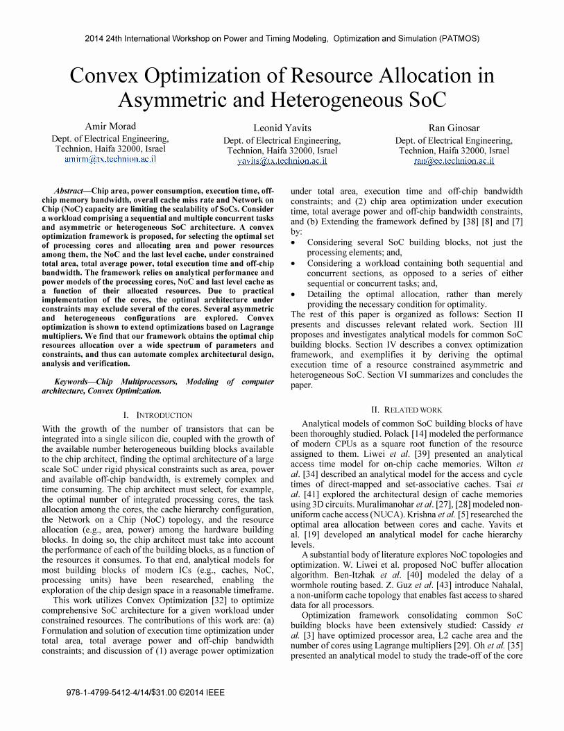
When optimiZing a modern SoC, the chip architect may need to optimize workloads containing both sequential and concurrent sections, and take into account additional building blocks such as caches and NoC while adhering to off-chip bandwidth limitations. Thus, the contribution of this paper is addressing a comprehensive research question: given (a) a SoC architecture consisting of last level cache (LLC), processing cores and a NoC interconnecting the cores and the LLC (see Figure 1); (b) workloads consisting of sequential and concurrent tasks (see Figure 2); and (c) physical resource constraints (area, power, execution time, off-chip bandwidth), what is the optimal selection of a subset of the available processing cores and what is the optimal resource allocation among all blocks. Further, the presented optimization methodology enables the SoC architect optimally select subset of the cores and allocate resources among the cores, LLC and NoC, without having to explore the design space in an iterative ad-hoc fashion.
Figure 1. Typical SoC architecture containing several processing cores,
LLC, NoC and Memory I/F.
I
I Figure 2. Typical workload
consisting of seq. and concurrent tasks
III. ANALY TICAL MODELS
In this section, we propose and investigate an analytical model for common building blocks of modern multiprocessors. For each block, we model the delay (e.g. , execution time, access time) and power, as a function of the resources it uses (e.g. , area).
A. Workload
Consider a typical workload consisting of sequential as well as M concurrent tasks, as depicted in Figure 2. Further, consider a SoC comprising N cores, each capable of executing the following: • Sequential (un-parallelizable) section: The sequential
portion of the workload cannot break into a finer granularity concurrent sub-tasks, and thus it is executed on a single core. The sequential section of the workload requires to seconds to execute on a reference processor of IPS=1 (Inst. Per Second). Any one of N available cores can accelerate the sequential section. The performance of core j is Per fj ( aj), relative to the performance on the reference processor, and is a function of its area aj. The acceleration function /j(aj) represents the inverted performance of corej:
(1)
The runtime of the sequential task running on core j having area aj is thus /j( aj) . to.
• Concurrent section: We assume that the concurrent portion of the workload is composed of Mtasks, and each task may run on any core. In a similar manner to sequential processing, each concurrent task i of the workload requires time ti to execute on a reference processor of IPS=1. The runtime of the /h task running on core j having area aj is
thus /j( aJ . ti· • Sequential - parallel synchronization: Concurrency incurs
data exchange between the sequential (first) core and the other cores at the beginning and the end of each concurrent section of the workload for subsequent processing. The data exchange entails transferring data from the LLC through the NoC into the private caches of the cores.
The performance of a core increases when additional area
2014 24th International Workshop on Power and Timing Modeling, Optimization and Simulation (PATMOS)
resources are assigned to it. Therefore, the acceleration functions /j (a j) are strictly decreasing. We asswne that the acceleration functions /j (a j) are convex and are continuously differentiable.
This paper studies the optimal resource allocation of a specific workload executing on application specific SoC, assuming that each task's runtime on a reference processor is known in advance. Further, we asswne that tasks runtime depends only on core's speedup function at its designated area, power (in a similar manner to [14][3][37][22][38][8]). Our model, however, does account for microarchitecture differences as each core may have its own area- and power-to- performance model. Our model may be utilized to perform early stage exploration of a suitable architecture. Early architecture exploration based on theoretical abstracted model, can eliminate many design cycles and iterations and expand the choice of alternatives that are too numerous for actual design explorations. Early exploration does not utilize simulation, and thus saves design time.
B. Processing Core
Following [14] and [37], the core's inverted performance may be written as follows (coefficients translating from area to performance units are scaled to unity):
1 fcore(acore) = --p (2)
ar;()re The exponent {3 typically varies from 0.3 to 0.7 [31]. The
higher the {3, the stronger the core is. For the purpose of our optimization framework, following [7], we modify the acceleration function (1) of core j to depend on both its area aj and its dynamic power Pj' as follows:
1 /j(aj, pj) =
P er/j(aj, pj) (3)
Note that Pj represents actual power dissipated in core j rather than the maximum power that can be consumed by that core, as determined by its area, maximum voltage, maximum frequency and other physical constraints; for instance, it is possible that at some optimum point for the entire chip, a particular core is operated at Pj < Pmaxj'
Area is a static resource, i.e. , it does not change during execution. Static power depends on temperature [18], and temperature, in turn, depends on power density (related to dynamic power). We shall separate the static power consumption of the core into two components, idle static power, and temperature induced static power. Assume that the SoC employs Dynamic Voltage and Frequency Scaling (DVFS). The idle static power is annotated as a manufacturing technology related constant SI multiplied by the core's allocated area aj representing the static power when: (a) gate temperature is at the low end of the operating conditions range; (b) core voltage is at the low end of the DVFS voltage range; and, (c) core frequency is at the low end of the DVFS frequency range. Within the normal operating temperature range (say, 55°C-85°C), leakage power consumption may be estimated using a linear function of temperature [42]. We can thus express the temperature induced static power as a manufacturing technology related constant S2 times its dynamic power Pj.
(4)
Note that in our analysis we choose to ignore floorplaninduced leakage power, that is, temperature increase due to the heat generated by adjacent cores. Given that the cores have large enough radial shape, floorplan induced leakage is limited to the boundary and hence is a second order effect on total leakage. Note however that this asswnption may not always hold. Given that the SoC employs DVFS, each core's frequency corresponds to its power budget, Pj' enabling clocking at a range of frequencies, from zero (when the core is idle) to Fmax (maximal frequency possible by the operating conditions and the physical constraints of the design). The maximal dynamic power of core j can be written as follows:
(5)
where al is the activity factor. Voltage is inversely proportional to gate delay, and thus it is proportional to frequency Vmaxj = a2Fmaxj, where a2 is a constant translating Hz to Volts. Capacitance Cj is proportional to area aj' Cj = a3aj' Assume that all cores are subject to the same activity factor al. Asswne further that all cores are driven by the same voltage range ('<Ij, Vmin :::; \.'i :::; Vmax). We can write (5) as:
Pmaxj = alCjFmaxj(a2Fmaxjl = aajF�axj (6)
where a is a constant absorbing aVa2 and a3' We can also model Pmax j = cjaj , where Cj = aF�axj is a constant translating units of area to power, in agreement with [1] and [25]. Next, assume that each core is driven at some operating frequency, Foper j' dissipating dynamic power Pj . Following (6):
(7)
Equation (7) complements [30] who noted through an empirical study that a typical CPU power is a polynomial function of frequency Pcore ex: r' where r] typically ranges from 1.5 (in a low power manufacturing technology) to 2.4 (in a high performance manufacturing technology). The present theoretical analysis leads to r] = 3 instead, but any other nwnber will do and will not significantly change our results. We annotate the normalized frequency of the core as Fnorm j' ranging from 0 (core is idle) to 1 (core is driven at maximal frequency corresponding to operating conditions and physical constraints of the design). Thus:
F . - Foper j - � - ..!!.L ( )1/3 ( )1/3
norm] - - -
Fmax j Pmax j cjaj (8)
Even when assigned with infinite power budget, the core's operating frequency cannot exceed its maximum frequency determined by the physical constraints of the design, thus (8) is revised as follows:
(9)
2014 24th International Workshop on Power and Timing Modeling, Optimization and Simulation (PATMOS)
Since the core's inverted performance is modeled as a power law with respect to its allocated area, we can write the acceleration function of a core as follows:
1 1 1 ((c-a .)1/3 ) F·(a· p.) = --- = - max .1......L 1 11 J' 1 fJ'F fJ· , aj ] normj aj ] Pj
(10)
Note that if core j is assigned with null power (Pj = 0), /j --7
00. Conversely, if core j is assigned with infmite power (Pj --7
00) , /j --7 aj -fJj. While considering asymmetric architectures, we focus on homogenous tasks and exclude task heterogeneity (for example, certain tasks may benefit from larger cache sizes, others may benefit from larger branch prediction buffer, etc.). Thus, we assume that tasks runtime depends only on the core's speedup function at its designated area. Given the core areas Acore = {av ... , aN} , and power allocation Pcore = {Pv ... , PN}, the execution time to of the sequential portion of the workload is determined by the fastest available core, thus:
N
Tseq � L /j( aj' Pseq) bO,jto ;=1
where, at the optimal point:
(1 : bi,j =
to: ith task is assigned to /h core
otherwise
(11)
(12)
Note that when the sequential portion of the workload is executed on some core, the dynamic power that is assigned to all other cores becomes available to it (up to its maximum possible power cjaj), thus:
N
Pseq = Pproc-Dynamic = L Pi i=1
Note further that a task is assigned to a single core. The area and power of core j, namely (aj' P j), may be 0 or positive, respectively. Core j execution time of the concurrent tasks assigned to it is:
7J � ,\,!=M
/j( aj, Pj) bi,jti = /j( aj, Pj) ,\,!=M
bi,jti (13) L!=l L!=l The total execution time of the concurrent section of the workload Tcon ' is determined by the last core to finish executing its allocated tasks, thus
Tcon � max(T1' Tz, ... , T N) (14)
The total execution time is:
Tproc = Tseq + Tcon (15)
Thus, the total average power dissipated by the cores is:
Pproc = Pproc-Static + Pproc-Dynamic (16)
C. Last Level Cache (LLC)
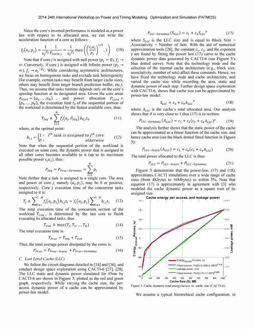
We follow the circuit diagrams detailed in [34] and [36], and conduct design space exploration using CACTI-6 [27], [28]. The LLC static and dynamic power simulated for 45nm by CACTI-6 are shown in Figure 3, plotted as the red and green graph, respectively. While varying the cache size, the peraccess dynamic power of a cache can be approximated by power-law model:
PLLC-Dynamic(SLLC> = C1 + CZSLLCY (17)
where SLLC is the LLC size and is equal to Block Size x
Associativity x Number of Sets. With the aid of numerical approximation tools [26], the constant c1, cz, and the exponent yare found by fitting the power law (17) curve to the cache dynamic power data generated by CACTI-6 (see Figure 3's blue dotted curve). Note that the technology node and the selection of the internal cache architecture (e.g. , block size, associativity, number of sets) affect these constants. Hence, we have fixed the technology node and cache architecture, and varied the cache size while recording the area, static and dynamic power of each step. Further design space exploration with CACTI-6, shows that cache size can be approximated by power-law model:
SLLC = C3 + C4ALL/ (18)
where ALLC is the cache's total allocated area. Our analysis shows that {) is very close to 1 thus (17) is re-written:
PUC-Dynamic(ALLC) = c1 + CZ(C3 + C4ALLC)Y (19)
The analysis further shows that the static power of the cache can be approximated as a linear function of the cache size, and hence cache area (see the black dotted fitted function in Figure 3):
PLLC-Static(ALLC> = Cs + C6(C3 + C4ALLC> (20)
The total power allocated to the LLC is thus:
Puc = PLLC-Static + Puc-Dynamic (21)
Figure 3 demonstrate that the power-law, (17) and (18), approximates CACTI simulations over a wide range of cache sizes (from 4Kbytes to 16Mbytes) to within 5%. Note that equation (17) is approximately in agreement with [3] who modeled the cache dynamic power as a square root of its assigned size.
1.8, Cache energy per access, and leakage power
r r r r ',8000
U5000 � 04000 {
(I) I � ""
, roo �
A--EnergYD;namc/Access, nJ rOOD
L 1 ----- Fitted function Pd(S)=O 168+0 158'SO 318 �. 1_
A' l- Leakage power, mW
,/ I -----, Fitted function: Ps(S)=70.1+ 7.63'SO.985 � 0 o 100 200 300 400 500 600 700 800 900 1000
Cache Size (5), MB Figure 3. Cache dynamic read energy/access vs. cache size (CACTI-6).
We assume a typical hierarchical cache configuration, in
2014 24th International Workshop on Power and Timing Modeling, Optimization and Simulation (PATMOS)
which each processing core contains a single private cache level, and all cores share the LLC. This framework can be extended to any number of private, shared or hybrid levels. Following [19], we assume that the access time of the LLC is approximated by power-law model:
(22)
Both T and the exponent p are found by fitting the power law (22) curve to the cache access time data generated by CACTI. For caches having several shared clients, the access time can be written as follows:
( SLLC )p tLLC = TNOC + T -N (23) Proc TNOC = ttransfer + tblocking + tcongestion
where Nproc is the number of shared cache clients (in our framework, the number of processing cores) and the LLC is fragmented, so that the more the processors, the smaller each fragment is and the shorter its access time. NoC delay TNOC is a sum of transfer delay, ttransfen blocking delay, tblocking and queuing (congestion) delay, tcongestion ' We adopt the analytical models for tblocking and tcongestion proposed by [39] and [40]. tblocking and tcongestion depend on a variety of parameters including the shared cache access rate RLLC' the network capacity, the number of cores etc. Those parameters except for RLLC and the number of cores, are not part of our optimization framework. Therefore we model both tblocking and tcongestion as function of R LLC , assuming the rest of
parameters are constant. Transfer delay, ttransfen is D (Fn), assuming 2-D mesh NoC [13]. The average memory delay is written as follows:
TLLC = ( 1- MRLLdtLLC + MRLLc(dAccess + dQueue) (24)
where dAccess is the DRAM access penalty and dQueue is the interconnect queuing delay. The LLC miss-rate, MRLLC, can be written as follows:
MRLLC = mcomp + (1- mcomp )CsharinglJSLLc/Nproc
(25)
where CSharing is the data sharing factor [3], and mcomp is the compulsory miss component reflecting access to data originated in remote (rather than in local) core [17]. Note that mcomp does not depend on the size of the processing cores' local cache. DRAM interconnect queuing delay dQueue can be presented as a function of the rate of access to off-chip M R LLC, the off-chip memory bandwidth, the number of processing cores etc. [5]. Those parameters except for MRLLC and the number of processing cores are not part of our framework. Hence we model dQueue as a function of MRLLC, assuming the rest of the parameters are constant. The off-chip bandwidth can be written as:
(26)
In real life, cache performance is affected by a combination of constrained chip resources. When LLC area budget is limited, the elevated miss rate causes the off-chip memory traffic to intensify, thus enlarging the total chip power. As a
result, the average memory delay is affected by longer DRAM queuing delays. When LLC area budget is substantial, LLC power consumption becomes the primary constraint as it becomes too large to power, while on the other hand, the decreased bandwidth reduces the total chip power. To that end, the optimal cache size should be obtained only within the framework of the entire chip. We thus include the DRAM pinout power dissipation into the optimization framework as follows:
PDDR = C DDRBWLLC (27)
where C DDR is a constant translating bandwidth (bit/second) to average power dissipated at SoC pinout.
D. Network on a Chip (NoC)
We assume a 2-D mesh NoC [13], with a transfer delay D( Fn). We assume that NoC hub blocks are identical and consume a fixed area, a NoC' Thus, the total NoC area is:
ANOC = (Nproc + 1LLC)a NOC (28)
where Nproc is the number of integrated processing cores (that is, the sum of processing cores which have been allocated area larger than 0). We further assume that the NoC blocks are constantly active and thus consume a fixed power, relative to the area:
PNoC = CApANOC (29)
where CAP is a constant translating units of area to power [12], [25]. Note that other NoC topology may be considered, such as Nahalal [43] that enables fast access to shared data for all processors, while preserving the vicinity of private data to each processor.
E. Total Resources
The combined area, power (static and dynamic) and execution time is a summary of all resources allocated to the processing cores, NoC and the LLC, respectively:
ATotal = ALLC + ANOC + Aproc S; ATotal Constraint PTotal = PLLC + PDDR + PNoC + Pproc
S; PTotal Constraint (30)
TTotal = TLLC + TNOC + Tproc S; TTotal Constraint BWTotal = BWLLC S; BWTotal Constraint
Note that the network delay, TNoC, is modeled as a part of the LLC's delay.
IV. CONVEX OPTIMIZATION
A convex function satisfies the inequality [(ax + py) S; alex) + P[(y) [32]. An optimization problem of finding some x' E X such that [(x') = min{f(x): x E X} where X c Iffi.n is the feasible set and [(x): Iffi.n � Iffi. is the objective, is called convex if X is a closed convex set and [(x) is convex on Iffi.n [16][9]. We extend the analysis of [7] by considering: (a) comprehensive SoC architecture having NoC and LLC; and (b) workload containing sequential and concurrent tasks, in four types of SoC architectures, each containing two cores, for the simplicity of exposition. • Asymmetric, unbalanced P (cf. (2)): the workload may be
distributed across up to two distinct cores, having
2014 24th International Workshop on Power and Timing Modeling, Optimization and Simulation (PATMOS)
unbalanced exponent � = {0.6, 0.4}, respectively. • Asymmetric, balanced �: the workload may be distributed
across up to two distinct cores, having balanced exponent � = {O.S, 0.5}, respectively.
• Heterogeneous, unbalanced �: the workload should be distributed across exactly two distinct cores, having unbalanced exponent � = {0.6, 0.4}, respectively.
• Heterogeneous, balanced � : the workload should be distributed across exactly two distinct cores, having balanced exponent � = {O.S, O.S}, respectively.
We further assume that each processing core contains a private L 1 cache. Each workload task is characterized by miss rates defined in [5] using PARSEC [10] and NAS [11], corresponding to the sequential-parallel synchronization data exchange. Further, we have applied assumptions similar to those used in [5], [20] and [35] for the constants described in (23) - (25). Our framework finds the optimal resource allocation in a broad spectrum of constraints. While we only exemplify execution time under constraints optlllllzation, our methodology can also be utilized for optimizing power under constraints and area under constraints [6].
Consider a synthetic workload consisting of a sequential task incurring execution time to = 40, and two concurrent tasks, incurring execution times tc = {SO,IO} on a reference processor, respectively. We wish to minimize the total execution time of a SoC consisting of processing cores, NoC and LLC, under total area, total average power and off-chip bandwidth constraints. We thus write our optimization problem as follows:
minimize TTotal {ALLc. ANOC.a V ... , a N' Pl' ... , PN} subject to: ATotal ::; ATotal Constraint
PTotal ::; PTotal Constraint BWTotal ::; BWTotal Constraint
(31)
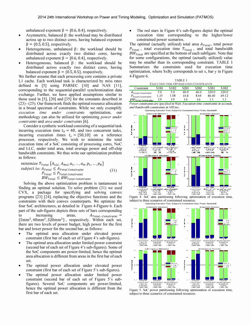
Solving the above optimization problem is tantamount to fmding an optimal solution. To solve problem (31) we used CVX, a package for specifying and solving convex programs [23] [24], replacing the objective functions and the constraints with their convex counterparts. We optimize the four SoC architectures, as detailed in Figure 4-Figure 6. Each part of the sub-figures depicts three sets of bars corresponding to increasing areas, ATotal-constraint = {Smm2, 40mm2, 320mm2} , respectively. Within each set, there are two levels of power budget, high power for the first bar and lower power for the second bar, as follows: • The optimal area allocation under elevated power
constraint (first bar of each set of Figure 4's sub-figures). • The optimal area allocation under limited power constraint
(second bar of each set of Figure 4's sub-figures). Some of the SoC components are power-limited, hence the optimal area allocation is different from areas in the first bar of each set.
• The optimal power allocation under elevated power constraint (first bar of each set of Figure 5's sub-figures).
• The optimal power allocation under limited power constraint (second bar of each set of Figure 5's subfigures). Several SoC components are power-limited, hence the optimal power allocation is different from the first bar of each set.
• The red stars in Figure 6's sub-figures depict the optimal execution time corresponding to the higher/lower constrained power scenarios.
The optimal (actually utilized) total area ATotaz, total power
PTotal , total execution time TTotal , and total bandwidth BWTotal are specified at the bottom of each subfigure. Note that for some configurations, the optimal (actually utilized) value may be smaller than its corresponding constraint. TABLE 1 Summarizes the constraints used for execution time optimization, where SxBy corresponds to set x, bar y in Figure 4-Figure 6.
TABLE I EXECUTION TIME OPTlMIZA TlON CONSTRAINTS
Constraint SIB I S1B2 S2Bl S2B2 S3Bl S3B2
ATotal Constraint 5.0 5.0 40.0 40.0 320.0 320.0
PTotal Constraint 1.35 1.08 10.8 8.64 86.40 69.12
BWTotalComtrajPl 1.9 1.9 1.6 1.6 1.1 1.1 P ower constraints are specified in Watt , Execution time constraints in seconds, and Bandwidth constraints in MB/sec.
Optimizing Execution Time, Subject to Constrained Area, POlNer, Band""';dth
(b)Asymmetric,Balancedfj
518115182 I 4_7mm212_smm2 I
1.3Wll.1W 10.8WIS.6W' 75_081137.4& 16.2&117_8&
1.9MBll.9MB 1.6MBll.6MB 1.1MBll.1MB 1.9MBll.9MB 1.6MBll.6MB 1.1MBll.1MB
Figure 4. SoC area partitioning following optimization of execution time, subject to three scenarios of constrained resources.
Optimizing Execution Time, Subject to Constrained Area, Power, BandWdth
(a)Asymmetric,Unbalanced p
51Bl151B2 ---':'� 'B� '''� 'B�' --,::,,:,,",�,,,",:,,� 5.Omm214.6mm2 4O.Omm2140.Omm2 320.Omm21320.Omm2
1.3W11.1W 1O.fN>Il8.fNV 85.CWI69.1W 58.3sIBO.2s 12.08113.08 4.0s 14.2s
1.7MBI1.6MB 1.6MBI1.6MB 1.lMBI1.1MB
(b) AsymmelTic, Balanced II
SlB11S1B2 --'::" ':'B'� '''� B'��'�'"� '''�'"�' --' 5.Omm2p.9mm2 4O.Omm2140.Omm2 320.Omm2132O.Omm2
1.3W11.1W 10.fN>II8.6W 85.2W169.1W 65·9s188.0s 16.2sl17.8s 6.0816.&
1.6MBI1.6MB 1.6MBI1.6MB 1.lMBIl.lMB
SlB11S1B2 52Bl152B2 53B1 153B2 SlB11S1B2 S2B11S2B2 S3B1IS3B2 5.Omm213.1mm2 4O.Omm2140.Omm2320.Omm21320.Omm2 4.7mm212.8mm2 4O.Omm2140.Omm2320.Omm2132O.Omm2
1.3W11.1W 10.fN>Il8.fNV 85.CWI69.1W 1.3W11.1W 10.fN>II8.6W 85.2W169.1W ·67.&1138.3s 12.08113.08 4.0s 14.2s ·75.0s1137As 16.2sl17.8s 6.0816.& 1.9MBI1.9MB 1.6MBI1.6MB 1.1MBI1.1MB l.9MBI1.9MB 1.6MBI1.6MB 1.1MBI1.1MB
Figure 5. SoC power partitioning following optimization of execution time, subject to three scenarios of constrained resources.
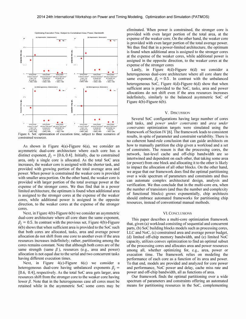
2014 24th International Workshop on Power and Timing Modeling, Optimization and Simulation (PATMOS)
i '" 75
j
,
,
Optimizing Execution Time, Subject to Constrained Area, Power, Bandwidth
(a)Asymmetrio= Unbalancedp
•
•
S1811S182 5.cxnm2I<1_Smm2
1_3Wll_1W 58_3sl8O_28
1.7MB 11.6MB
0----,,",,"
• • • •
528115282 $38115382 4O_0mm21'40_0mm2 32o_Omm2p20_omm2
10_8WI8_6W 85_OWI69_1W 12_05113_0s 4_0514_2s
1_6MBII_6MB 1_1MBll_1MB
Ie) Hetelogeneous, Unbalanced II
• 0----,,",,"
•
• • • •
,
,
,
,
(b) Asymmetric Balanced fI
•
•
S1Bl1S1B2 5_0mm2p_9mm2
1.3Wll.1W 65_95188_0s
1_6M811_6MB
C=*,_n"",
• • • •
828115282 $38115382 <lO_Omm2140.cxnm2 320_0mm2p20_0mm2
10_8Wf8_6W 85.2WI69.1W 16_25117_85 6_0s16_58
I_SMBI1_6MB 1_1MBll_1MB
(d) Hetelogeneous, Balanced II
• c.�
• • • •
S281 282 S1811S182 IS 838118382 S1811S182 828118282 838118382 5.Omm213.1mm2 4O.Omm2140.0mm2 320.Omm21320.0mm2 4.7mm212.8mm2 4O.0mm2140.Omm2 320.0mm21320.0mm2
1.3W11.1W 10.8WI8.6W 85.OWI69.1W 1.3WI1.1W 10.8Wi8.6W 85.2WI69.1W 67.5sI138.3s 12.0s113.0s 4.0s14.2s ·75.0s1137.4s 16.2sl17.8s 6.0s16.5s 1.9MBI1.9MB 1.6MBI1.6MB 1.1MBI1.1MB 1.9MBI1.9MB 1.6MBI1.6MB 1.1MBI1.1MB
Figure 6. SoC optimization of execution time, subject to three scenarios of constrained resources.
As shown in Figure 4(a)-Figure 6(a), we consider an asymmetric dual-core architecture where each core has a distinct exponent, {3j = {0.6, 0.4}. Initially, due to constrained area, only a single core is allocated. As the total SoC area increases, the weaker core is assigned with the shorter task, and provided with growing portion of the total average area and power. When power is constrained the weaker core is provided with smaller area portion. On the other hand, the weaker core is provided with larger portion of the total average power at the expense of the stronger cores. We thus find that in a power limited architecture, the optimum is found when additional area is assigned to the stronger cores at the expense of the weaker cores, while additional power is assigned in the opposite direction, to the weaker cores at the expense of the stronger cores.
Next, in Figure 4(b)-Figure 6(b) we consider an asymmetric dual-core architecture where all core share the same exponent, {3j = 0.5. In contrast with the previous set, Figure 4(b)-Figure 6(b) shows that when sufficient area is provided to the SoC such that both cores are allocated, tasks, area and average power allocation do not shift from one core to another even if the area resources increases indefinitely; rather, partitioning among the cores remains constant. Note that although both cores are of the same strength (same {3), resources (e.g. , area and power) allocation is not equal due to the serial and two concurrent tasks having different execution times.
Next, in Figure 4(c)-Figure 6(c) we consider a heterogeneous dual-core having unbalanced exponents {3j = {0.6, 0.4}, respectively. As the total SoC area gets larger, area resources shift from the stronger core to the weaker core having lower {3. Note that in the heterogeneous case all cores must be retained while in the asymmetric SoC some cores may be
eliminated. When power is constrained, the stronger core is provided with even larger portion of the total area, at the expense of the weaker core. On the other hand, the weaker core is provided with even larger portion of the total average power. We thus find that in a power-limited architecture, the optimum is found when additional area is assigned to the stronger cores at the expense of the weaker cores, while additional power is assigned in the opposite direction, to the weaker cores at the expense of the stronger cores
Lastly, in Figure 4(d)-Figure 6(d) we consider a heterogeneous dual-core architecture where all core share the same exponent, {3j = 0.5 . In contrast with the unbalanced
heterogeneous SoC, Figure 4(d)-Figure 6(d) show that when sufficient area is provided to the SoC, tasks, area and power allocations do not shift even if the area resources increases indefmitely, similarly to the balanced asymmetric SoC of Figure 4(b)-Figure 6(b).
V. DISCUSSION
Several SoC configurations having large number of cores and tasks, and power under constraints and area under constraints optimization targets were simulated using the framework of Section IV [6]. The framework leads to consistent results, in spite of parameter and constraint variability. There is no coherent hand-rule conclusion that can guide architects on how to manually partition the chip given a workload and a set of constraints. The reason is that the processing cores, the network, last-level cache and off-chip bandwidth are so intertwined and dependent on each other, that taking some area (or power) from one block and allocating it to the other is likely to impact the allocation of all other blocks. On the other hand, we argue that our framework does find the optimal partitioning over a wide spectrum of parameters and constraints and thus can automate complex architectural design, analysis and verification. We thus conclude that in the multi-core era, when the number of transistors (and thus the number and complexity of functional blocks) grows exponentially, chip architects should embrace automated frameworks for partitioning chip resources, instead of conventional manual methods.
VI. CONCLUSIONS
This paper describes a multi-core optimization framework that, given (a) workload consisting of sequential and concurrent parts, (b) SoC building blocks models such as processing cores, LLC and NoC, (c) constrained area and average power budget, (d) limited off-chip memory bandwidth, and (e) limited NoC capacity, utilizes convex optimization to fmd an optimal subset of the processing cores and allocates area and power resources among all, whether optimizing for, e.g. , area, power or execution time. The framework relies on modeling the performance of each core as a function of its area and power. To that end, models are provided and analyzed for core power and performance, NoC power and delay, cache miss rate and power and off-chip bandwidth, all as functions of area.
Our framework finds the optimal partitioning over a wide spectrum of parameters and constraints offering an automated means for partitioning resources in the SoC, complementing
2014 24th International Workshop on Power and Timing Modeling, Optimization and Simulation (PATMOS)
conventional manual methods. This paper extends and generalizes previous Lagrange based
optimization frameworks [38][8] and [7]. One of the potential applications of this framework is optimizing the average power or energy of a given workload, executing on a fabricated semiconductor SoC (where area resources have been already partitioned). In such a case, for example, a real-time workload is given with known execution time upper bounds, and the average power budget is optimally partitioned so as to minimize total average power or energy. Our framework offers an efficient alternative to iterative ad-hoc methods for exploring the design space.
ACKNOW LEDGMENT
This research was funded in part by the Intel Collaborative Research Institute for Computational Intelligence (ICRI-CI) and by Hasso-Plattner Institute (HPI).
REFERENCES
[I] A. Agarwal et aI. "Core Count vs. Cache Size for Manycore Architectures in the Cloud." (2010).
[2] A. Alameldeen, "Using compression to improve chip multiprocessor perfonnance", PhD thesis, University of Wisconsin, Madison, WI, 2006.
[3] A. Cassidy and A. Andreou, "Beyond Amdahl Law - An objective fimction that links perfonnance gains to delay and energy", iEEE Transactions on Computers, vol. 61, no. 8, pp. 111O-1126, Aug 2012.
[4] A. Elyada, R. Ginosar, U. Weiser, "Low-Complexity Policies for EnergyPerfonnance Tradeoff in Chip-Multi-Processors," iEEE Transactions on U?ry Large Scale integration (VLSJ) Systems, Volume: 16, Issue: 9, 2008, Page(s): 1243 - 1248.
[5] A. Krishna, A. Samih, and Y Solihin. "Data sharing in multi-threaded applications and its impact on chip design",lSPASS', 2012.
[6] A. Morad, L. Yavits and R. Ginosar, "Convex Optimization of Resource Allocation in Asymmetric and Heterogeneous Multicore," 2014
[7] A. Morad, T. Morad, L. Yavits and R. Ginosar, "Optimization of Asvmmetric and Heterogeneous MultiCore," 2013
[8] A. Morad, T. Morad, L. Yavits, R. Ginosar, U. C. Weiser. "Generalized MultiAmdahl: Optimization of Heterogeneous Multi-Accelerator SOC," iEEE Computer Architecture Letters, 2012.
[9] Ben-Tal, Aharon; Nemirovskii, Arkadii Semenovich (2001). Lectures on modem convex optimization: analysis, algorithms, and engineering applications. pp. 335-336.
[10] C. Bienia et al., "The PARSEC Benchmark Suite: Characterization and Architectural Implications", PACT2008 ..
[II] D. Bailey, et al. "The NAS Parallel Benchmarks", intI. Journal of Supercomputer Applications, 5(3):63--73, 1991
[12] D. H. Woo and H. H. S. Lee. "Extending Amdahl's law for energy-efficient computing in the many-core era." Computer, 41(12):24-31, 2008.
[13] D. Wentzlaf( et al., "Core Count vs. Cache Size for Manycore Architectures in the Cloud." Tech. Rep. MlT-CSAlL-TR-2010-008, MIT, 2010.
[14] F. Pollack. "New Microarchitecture Challenges in the Coming Generations of CMOS Process Technologies," Keynote, Micro 32, 1999, www.intel.com/researchimrVLibraty/micro32Kevnote.pdf
[15] G. Loh, "The cost of uncore in throughput-{)riented many-core processors", Workshop on Architectures and Languages for Throughput Applications. 2008.
[16] Hiriart-Urruty, Jean-Baptiste; Lemarechal, Claude (1996). Convex analysis and minimization algorithms: Fundamentals. p. 291.
[17] Huh et al., "Exploring the design space of future CMPs," PACT, 2001. [18] K. BaneIjee et aI., "A self -<XJnsistent junction temperature estimation methodology
for nanometer scale ICs with implications for perfonnance and thennal management," IEEE IEDM, 2003, pp. 887-890.
[19] L. Yavits, A. Morad, R. Ginosar, "Cache Hierarchy Optimization," iEEE Computer Architecture Letters, 2013
[20] L. Yavits, A. Morad, R. Ginosar, "The effect of communication and synchronization on Amdahl's law in multicore systems", Technion TR, http://webee.technion.ac.il/publication-linkiindexlicV611.
[21] L. Zhao and R. Tyer, et al., "Perfonnance, Area, and Bandwidth Implications for Large scale CMP Cache Design", CMP-MSI, 2007.
[22] M. D. Hill and M. R. Marty. "Amdahl's Law in the Multicore Era," iEEE Computer, July 2008.
[23] M. Grant and S. Boyd. "CVX: Matlab software for disciplined convex programming, version 2.0 beta" http://cvxr.com/c� September 2013.
[24] M. Grant and S. Boyd. Graph implementations for nonsmooth convex programs, Recent Advances in Learning and Control (a tribute to M. Vidyasagar), V Blondel, S. Boyd, and H. Kimura, editors, pages 95-110, Lecture Notes in Control and information Sciences, Springer, 2008. http://stanford.edul-boycVgraph dcp.htrnl.
[25] Mark Hempstead, Gu-Yeon Wei, and David Brooks. "Navigo: An early-stage model to study power-constrained architectures and specialization," ISCA Workshop on Modeling, Benchmarking, and Simulations (MoBS). Austin TX, June 2009
[26] MATLAB Optimization Toolbox Release 2012b, The MathWorks, Inc., Natick, Massachusetts, United States. "Isqcurvefit" solver, ht1!J://www.mathworks.com/helP/optimlugj]sgcurvefithtrnl
[27] N. Muralimanohar, R. Balasubramonian, and N. Jouppi, "Cacti 6.0: A tool to understand large caches." University of Utah and Hewlett Packard Laboratories, Tech. Rep (2009).
[28] N. Muralimanohar, R. Balasubramonian, and N. Joupp� "Optimizing NUCA Organizations and Wiring Alternatives for Large Caches with CACTI 6.0", MICRO, pp. 3--14, 2007.
[29] R. T. Rockefellar. "Lagrange multipliers and optimality", SIAM Review, vol. 35, pp. 183--283, 1993.
[30] Rotem, E.; Ginosar, R.; Weiser, u.; Mendelson, A., "Energy Aware Race to Halt: A Down to EARtH Approach for Platfonn Energy Management;" Computer Architecture Letters, vol.Pp, no.99, pp.l,I, O. doi: 1O.l1091L-CA.2012.32
[31] S. Borkar. "Thousand Core Chips: A Technology Perspective," Proc. ACMliEEE 44th Design Automation Con! (DAC), 2007, pp. 746-749.
[32] S. Boyd, L. Vandenberghe, "Convex optimization", Cambridge university press, 2004.
[33] S. Natarajan, S. Narayanan, B. Swamy, and A. Seznec. "Modeling multi-threaded programs execution time in the many-core era." (2013).
[34] S. Wilton and N. Jouppi, "An Enhanced Access and Cycle Time Model for On-Chip Caches ", WRL Research Report 93/5, 1994.
[35] T. Oh et al., "An Analytical Model to Study Optimal Area Breakdown between Cores and Caches in a Chip Multiprocessor," IEEE Computer Society Annual Symposium on VLST, 2009, pp. 181-186.
[36] T. Wada, S. Rajan, , S. Przybylski, "An Analytical Access Time Model for On-Chip Cache Memories", IEEE Journal of solid-state circuits, vol. 27. no. 8, August 1992.
[37] T. Y Morad, U. C. Weiser, A. Kolodny, M. Valero and E. Ayguade. "Perfonnance, power efficiency, and scalability of asymmetric cluster chip multiprocessors," iEEE Computer Architecture Letters, vol. 4, 2005.
[38] T. Zidenberg, I. Keslassy and U. C. Weiser. "MultiAmdahl: How Should T Divide My Heterogeneous Chip?," IEEE Computer Architecture Letters, 2012.
[39] W. Liwei et al. "Application specific buffer allocation for wonnhole routing Networks-{)n-Chip", Network on Chip Architectures, 2008, 37.
[40] Y Ben-Itzhak, I. Cidon, A. Kolodny. "Delay analysis of wonnhole based heterogeneous NOC", Fifth IEEE! ACM International Symposium on Networks on Chip, 2011.
[41] Y. Tsai, Y Xie, V Narayanan, and M. J. Irwin, "Three-Dimensional Cache Design Exploration Using 3OCacti", ICCD, pp. 519-524, 2005.
[42] Yongpan Liu et al., "Accurate Temperature-Dependent Integrated Circuit Leakage Power Estimation is Easy," Design, Automation & Test in Europe Conforence & Exhibition, 2007. DATE '07 , vol., no., pp.l,6, 16-20 April 2007, doi: 1O.1109IDATE.2007.364517
[43] Z. Guz, Keidar, Idit, Avinoam Kolodny, and Uri C. Weiser. "Nahalal: Memory Organization for Chip MUltiprocessors." Technion-Dr; Department qf Electrical Engineering, 2006.