Controllable and Rapid Synthesis of High-Quality and Large-Area Bernal Stacked Bilayer Graphene...
9
Controllable and Rapid Synthesis of High-Quality and Large-Area Bernal Stacked Bilayer Graphene Using Chemical Vapor Deposition Wei Liu, † Stephan Kraemer, ‡ Deblina Sarkar, † Hong Li, † Pulickel M. Ajayan, § and Kaustav Banerjee* ,† † Department of Electrical and Computer Engineering and ‡ Department of Materials Science and Engineering, University of California, Santa Barbara, California 93106, United States § Department of Mechanical Engineering & Materials Science, Rice University, Houston, Texas 77005, United States * S Supporting Information ABSTRACT: Bilayer graphene has attracted wide attention due to its unique band structure and bandgap tunability under specific (Bernal or AB) stacking order. However, it remains challenging to tailor the stacking order and to simultaneously produce large-scale and high-quality bilayer graphene. This work introduces a fast and reliable method of growing high-quality Bernal stacked large-area (>3 in. × 3 in.) bilayer graphene film or trilayer graphene domains (30 μm × 30 μm) using chemical vapor deposition (CVD) on engineered Cu−Ni alloy catalyst films. The AB stacking order is evaluated by Raman spectra, electron diffraction pattern, and dual gate field-effect-transistor (FET) measurements, and a near-perfect AB stacked bilayer graphene coverage (>98%) is obtained. The synthesized bilayer and trilayer graphene with Bernal stacking exhibit electron mobility as high as 3450 cm 2 /(V·s) and 1500 cm 2 /(V·s), respectively, indicating comparable quality with respect to exfoliated bilayer and trilayer graphene. The record high (for CVD bilayer graphene) ON to OFF current ratios (up to 15) obtained for a large number (>50) of dual-gated FETs fabricated at random across the large-area bilayer graphene film also corroborates the success of our synthesis technique. Moreover, through catalyst engineering, growth optimization, and element analysis of catalyst, it is shown that achieving surface catalytic graphene growth mode and precise control of surface carbon concentration are key factors determining the growth of high quality and large area Bernal stacked bilayer graphene on Cu−Ni alloy. This discovery can not only open up new vistas for large-scale electronic and photonic device applications of graphene but also facilitate exploration of novel heterostructures formed with emerging beyond graphene two-dimensional atomic crystals. KEYWORDS: bilayer graphene, AB stacked graphene, chemical vapor deposition, Cu−Ni alloy, surface catalytic growth ■ INTRODUCTION Graphene, the first stable and thinnest two-dimensional (2D) material, which consists of a single layer of sp 2 -hybridized carbon atoms, has attracted wide interest due to its outstanding electrical and thermal properties and promising applications as electronic and photonic devices; 1−4 however, many of those applications are significantly restricted by the zero band gap of graphene 5 arising due to the inherent symmetry in its structure. Hence, opening a band gap in graphene has become an extremely important topic in the field of graphene nano- electronics. 6−10 In such circumstances, various methods have been explored to open a bandgap in graphene, through physical confinement of the carriers such as by patterning graphene into graphene nanoribbons (GNRs) 6 and unzipping carbon nano- tubes (CNTs) into GNRs. 11,12 However, those methods remain challenging either due to lack of control of the width and edge roughness of GNRs or precisely aligning CNTs on the substrate. Alternatively, Bernal (AB) stacked bilayer graphene can exhibit a bandgap if the symmetry of the electron wave functions in the direction perpendicular to the bilayer can be broken by inducing a potential difference between the two adjacent layers. In fact, bandgap of up to 0.25 eV can be induced when an electric displacement field is built up between the graphene layers by applying a perpendicular electric field, which has been proven by theory and experiments. 9,13,14 Thus, this bandgap tunability property provides a great opportunity for bilayer graphene to be widely used in electronic and photonic devices. Moreover, the transferability of such graphene layers to any desired substrate made of other 2D nanomaterials with a wide range of bandgaps, such as h-BN (∼5 eV) and transition metal dichalcogenides including MoS 2 and WSe 2 (1.1−2.2 eV), can be exploited to build unique heterostructure devices. In addition, high-transmittance, high- conductivity, and high-flexibility as well as impermeability to moisture (leading to improved reliability) make few layer (2−3 layer) graphene a promising electrode material for a variety of transparent conductor applications. Received: July 6, 2013 Revised: October 9, 2013 Article pubs.acs.org/cm © XXXX American Chemical Society A dx.doi.org/10.1021/cm4021854 | Chem. Mater. XXXX, XXX, XXX−XXX
Transcript of Controllable and Rapid Synthesis of High-Quality and Large-Area Bernal Stacked Bilayer Graphene...
Controllable and Rapid Synthesis of High-Quality and Large-AreaBernal Stacked Bilayer Graphene Using Chemical Vapor DepositionWei Liu,† Stephan Kraemer,‡ Deblina Sarkar,† Hong Li,† Pulickel M. Ajayan,§ and Kaustav Banerjee*,†
†Department of Electrical and Computer Engineering and ‡Department of Materials Science and Engineering, University ofCalifornia, Santa Barbara, California 93106, United States§Department of Mechanical Engineering & Materials Science, Rice University, Houston, Texas 77005, United States
*S Supporting Information
ABSTRACT: Bilayer graphene has attracted wide attention due toits unique band structure and bandgap tunability under specific(Bernal or AB) stacking order. However, it remains challenging totailor the stacking order and to simultaneously produce large-scaleand high-quality bilayer graphene. This work introduces a fast andreliable method of growing high-quality Bernal stacked large-area(>3 in. × 3 in.) bilayer graphene film or trilayer graphene domains(30 μm × 30 μm) using chemical vapor deposition (CVD) onengineered Cu−Ni alloy catalyst films. The AB stacking order isevaluated by Raman spectra, electron diffraction pattern, and dualgate field-effect-transistor (FET) measurements, and a near-perfectAB stacked bilayer graphene coverage (>98%) is obtained. Thesynthesized bilayer and trilayer graphene with Bernal stackingexhibit electron mobility as high as 3450 cm2/(V·s) and 1500 cm2/(V·s), respectively, indicating comparable quality with respectto exfoliated bilayer and trilayer graphene. The record high (for CVD bilayer graphene) ON to OFF current ratios (up to 15)obtained for a large number (>50) of dual-gated FETs fabricated at random across the large-area bilayer graphene film alsocorroborates the success of our synthesis technique. Moreover, through catalyst engineering, growth optimization, and elementanalysis of catalyst, it is shown that achieving surface catalytic graphene growth mode and precise control of surface carbonconcentration are key factors determining the growth of high quality and large area Bernal stacked bilayer graphene on Cu−Nialloy. This discovery can not only open up new vistas for large-scale electronic and photonic device applications of graphene butalso facilitate exploration of novel heterostructures formed with emerging beyond graphene two-dimensional atomic crystals.
KEYWORDS: bilayer graphene, AB stacked graphene, chemical vapor deposition, Cu−Ni alloy, surface catalytic growth
■ INTRODUCTION
Graphene, the first stable and thinnest two-dimensional (2D)material, which consists of a single layer of sp2-hybridizedcarbon atoms, has attracted wide interest due to its outstandingelectrical and thermal properties and promising applications aselectronic and photonic devices;1−4 however, many of thoseapplications are significantly restricted by the zero band gap ofgraphene5 arising due to the inherent symmetry in its structure.Hence, opening a band gap in graphene has become anextremely important topic in the field of graphene nano-electronics.6−10 In such circumstances, various methods havebeen explored to open a bandgap in graphene, through physicalconfinement of the carriers such as by patterning graphene intographene nanoribbons (GNRs)6 and unzipping carbon nano-tubes (CNTs) into GNRs.11,12 However, those methodsremain challenging either due to lack of control of the widthand edge roughness of GNRs or precisely aligning CNTs onthe substrate. Alternatively, Bernal (AB) stacked bilayergraphene can exhibit a bandgap if the symmetry of the electronwave functions in the direction perpendicular to the bilayer canbe broken by inducing a potential difference between the two
adjacent layers. In fact, bandgap of up to 0.25 eV can beinduced when an electric displacement field is built up betweenthe graphene layers by applying a perpendicular electric field,which has been proven by theory and experiments.9,13,14 Thus,this bandgap tunability property provides a great opportunityfor bilayer graphene to be widely used in electronic andphotonic devices. Moreover, the transferability of suchgraphene layers to any desired substrate made of other 2Dnanomaterials with a wide range of bandgaps, such as h-BN(∼5 eV) and transition metal dichalcogenides including MoS2and WSe2 (1.1−2.2 eV), can be exploited to build uniqueheterostructure devices. In addition, high-transmittance, high-conductivity, and high-flexibility as well as impermeability tomoisture (leading to improved reliability) make few layer (2−3layer) graphene a promising electrode material for a variety oftransparent conductor applications.
Received: July 6, 2013Revised: October 9, 2013
Article
pubs.acs.org/cm
© XXXX American Chemical Society A dx.doi.org/10.1021/cm4021854 | Chem. Mater. XXXX, XXX, XXX−XXX

Until recently, the most reliable way to produce AB stackedbilayer graphene is exfoliation of natural graphite, HighlyOrdered Pyrolytic Graphite (HOPG), or ionic graphiteintercalation compounds that are inherently AB stacked, bymicromechanical method or sonication method.9,15 However,these methods are not applicable for scalable manufacturing ofmicroelectronic devices and circuits. Therefore, it is particularlyimportant to develop a scalable synthesis method such as CVDmethod that could effectively control the number of graphenelayers as well as the stacking order, to enable large-scaleproduction of AB stacked bilayer graphene. Recently, bilayerand few layer graphene growth have been demonstrated ontransition metals, such as Ni and Cu, using the CVDmethod.16−21 However, few layer graphene grown on Ni16,17
by CVD tends to be disordered, wherein graphene layers arerandomly rotated. Cu has also shown the capability of growingbilayer and few layer graphene domains under certain growthconditions.18−22 However, several works have shown that onlypart of the synthesized bilayer or few layer graphene on pureCu exhibit AB stacking order.19,21,23 In fact, it is difficult toprovide sufficient carbon atoms for uniform few layer graphenegrowth on pure Cu surface19,21,24 because of Cu’s weakcapability of decomposing hydrocarbons.24,25 Therefore, bilayergraphene growth22,26 on Cu needs a very complicated processand a long growth time (several hours), which are not suitablefor large scale production. Hence, creating a reliable and fastmethod to synthesize large-scale and high-quality AB stackedbilayer graphene by general CVD technique in a controllablemanner remains a critical obstacle in developing electronicapplications of graphene. Recently, binary metal alloy catalystssuch as Cu−Ni27−29 have shown high capability in controlling
the number of graphene layers. The Cu−Ni alloy system hasbeen widely studied showing that the Cu/Ni ratio at the metalsurface can be tuned by varying the bulk Cu/Ni ratio orannealing temperature,30 indicating the possibility of tuning thegraphene growth on the Cu−Ni surface. It is well-known thatthe stacking order of few layer graphene growing from a carbonprecipitation process is non-AB.16 Therefore, it is important toavoid the carbon segregation process for achieving AB stackedgraphene growth. Importantly, in the Cu−Ni alloy system, Cuatoms tend to segregate to the topmost few atomic layers,forming a Cu rich surface.31 This Cu rich topmost surface couldgreatly suppress carbon solubility and the segregation processleading to the possibility of controlling the stacking order of afew layers of graphene. Hence, all of the above facts indicatethat the stacking order of graphene could be tuned byengineering the Cu−Ni stoichiometry under certain growthconditions (Figure 1a).Here, we report a versatile CVD graphene synthesis
technique employing a stoichiometry engineered Cu−Nicatalyst system, which can grow large-scale high-quality ABstacked bilayer graphene with high probability in a few minutes.Our study also establishes that the surface catalytic effect is themain mechanism for AB stacked bilayer graphene growth onCu−Ni, which is confirmed by the catalyst component analysisand temperature dependent graphene growth. The method wehave developed is the first one that is capable of synthesizinglarge area Bernal stacked bilayer and trilayer graphene in a fastand controllable manner, which is necessary for large scaleproduction.
Figure 1. (a) Schematic of catalyst engineered graphene growth process on Cu−Ni alloy via surface catalytic mode by suppressing carbonprecipitation. The yellow region at the top of the Cu−Ni layer indicates the concentration gradient of Cu. (b) Digital images of Cu−Ni (1200/400nm) film before (left) and after (right) graphene growth. (c) XRD spectra of the Cu−Ni catalyst after graphene growth. The peaks shown in (c)indicate that Cu-Ni alloy is formed after annealing and graphene growth process. (d) SEM image of graphene grown simultaneously on Cu−Ni alloy(left) and high purity Cu film (right), taken from the green circle area in (b). (e) Digital images of monolayer (left) and bilayer (right) graphene onquartz plates. Bilayer graphene is obtained under a different growth condition as shown in Figure 2. (f) Time dependent graphene growth (withcorresponding Raman spectra) on Cu−Ni (1200/400 nm) film, graphene growth condition is 920 °C, 0.5 mbar, and 1 sccm CH4/5 sccm H2 for 2,10, and 30 min. Monolayer graphene covers the Cu−Ni alloy surface in 2 min, and increasing the growth time beyond that still yields monolayergraphene.
Chemistry of Materials Article
dx.doi.org/10.1021/cm4021854 | Chem. Mater. XXXX, XXX, XXX−XXXB
■ EXPERIMENTAL SECTIONThrough graphene growth optimization, we found that Cu−Ni with aratio of 1200/400 nm (1200 nm Cu film was deposited on top of 400nm Ni) is the best catalyst for AB stacked bilayer growth. In this work,all of the characterizations were carried out on the samples grown on1200/400 nm Cu−Ni under the optimal growth conditions as shownin Supporting Information S1. Cu−Ni and high purity Cu (99.999%)films (Figure 1b, left) formed side by side on the same substrate arestudied at first to compare their capabilities of graphene growth.Graphene growth was carried out at the optimal conditions for bilayergraphene growth as described in Supporting Information Figure S1b.We also deposited Cu−Ni film with fixed Cu/Ni ratio (3:1) using
commercial Cu−Ni alloy target and obtained identical graphenegrowth results with respect to the deposited Cu−Ni film (Cu filmdeposited on top of Ni). In this study we only discuss graphenegrowth results using deposited Cu−Ni film as catalyst. Figure 1dshows the SEM image of the boundary area between the Cu−Ni andCu films after graphene growth under the same growth conditions. Itclearly shows that the contrast of the Cu−Ni area is darker than that ofthe adjacent pure Cu area. This difference in the contrast indicates thatthe number of graphene layers grown on the Cu−Ni alloy is largerthan one because high purity Cu (99.999%) films tend to growmonolayer graphene.20 Figure 1e displays the digital images of thetransferred graphene on quartz plates, which are grown on Cu−Ni(1200/400 nm) film (right) and high purity Cu foil (99.999%) (left)under the same growth conditions. The difference in optical contrastsis obvious and agrees with the results of the transmittancemeasurements (Supporting Information S2). The measured trans-mittance of the graphene grown on Cu−Ni (1200/400 nm) film is94% at 550 nm wavelength, in agreement with the reported value forbilayer graphene.32 This transmittance value is lower than that of themonolayer graphene (97% transmittance at 550 nm wavelengthmeasured on a sample grown on pure Cu foil). Hence, Cu−Ni alloyhas a higher capability to decompose methane than Cu under the samegrowth conditions.
■ RESULTS AND DISCUSSION
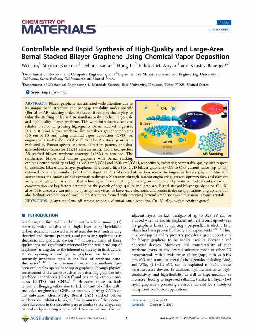
Contrary to Cu that is known to exhibit weak capability ofdecomposing methane, Cu−Ni alloy can easily decomposehydrocarbons and provide sufficient carbon atoms on thecatalyst surface, leading to the growth of graphene within ashort time. Cu−Ni alloy can be covered by monolayergraphene in a short time (less than 20 s as shown in theSupporting Information S3). Once the surface of Cu−Ni alloyis covered by graphene, graphene growth will be terminatedbecause methane cannot decompose on top of graphene.Usually, monolayer graphene can cover the entire surface ofCu−Ni alloy in 2 min (Figure 1f). However, with increase intime, the number of graphene layers on Cu−Ni alloy does notincrease any further and only monolayer graphene is obtainedeven after exposure to methane for a long time (30 min).Hence, time dependent growth (Figure 1f) can prove thatgraphene growth on Cu−Ni alloy surface obeys surface catalyticmode at lower partial pressure of methane (less than 0.003mbar). The number of graphene layers is primarily determinedby the Cu−Ni ratio, growth pressure and methane partialpressure. As mentioned in previous section, graphene growthon Cu−Ni alloy surface obeys the surface catalytic mode at lowmethane partial pressure. When the flow rate of methane isincreased to 8 sccm at 0.5 mbar, 80% of the graphene film iscovered by bilayer domains (Figure 2a). However, the size ofbilayer domains varies from 5 to 10 μm (Figure 2a) indicatingthe formation of a large number of nucleation centers on thesurface of Cu−Ni alloy. It has been found that it is possible toreduce the density of nucleation centers by decreasing thepartial pressure of hydrocarbon.25 After tuning the flow rate ofmethane to 3 sccm at 0.1 mbar, large bilayer domains (30−60μm) with low density appear on Cu−Ni alloy surface (as shownin Figure 2b). However, bilayer graphene regions still cannotcover the entire synthesized Cu−Ni substrate indicating that
Figure 2. Optimization of 2−3 layer graphene growth on Cu−Ni (1200/400 nm) film. Before flowing methane, Cu−Ni film was annealed at 990 °Cand 20 mbar and in 100 sccm H2/150 sccm Ar for 30 min. The growth temperature is 920 °C. (a) 0.5 mbar, 5 sccm H2, 8 sccm CH4, for 120 s. (b, c,and d) 0.1 mbar, 5 sccm H2, for 120 s with 3 sccm CH4, 6 sccm CH4, and 8 sccm CH4, respectively. Scale bar is 30 μm for (a) to (d). (e) Schematicof bilayer graphene growth mechanism on Cu−Ni alloy surface. (f, g) 0.2 mbar, 5 sccm H2, for 120 s with 8 sccm CH4 and 10 sccm CH4,respectively. Scale bar is 30 μm for (f) to (g). (h) Optical image of the contiguous area between two bilayer graphene domains. Scale bar is 20 μm for(h). (i) Raman mapping of 2D peak intensity of the contiguous area taken in the white circle in (h). (j) Digital image of bilayer graphene on 300 nmSiO2/Si, the size of the graphene is around 3 in. × 3 in. Raman measurements were performed with a Horiba JY Aramis Raman Microscope systemusing the 632 nm laser as the excitation source. The spectra were measured in the backscattering configuration using a 100X objective and a 600grooves/mm grating.
Chemistry of Materials Article
dx.doi.org/10.1021/cm4021854 | Chem. Mater. XXXX, XXX, XXX−XXXC

there is an insufficient number of carbon atoms available for thesecond layer growth (Figure 2e). Along with increase in theflow rate of methane (Figure 2b−d), the size of the bilayerdomains increase and eventually the Cu−Ni alloy surface iscovered by bilayer graphene (Figure 2d). It is interesting tonote that after two bilayer domains merge into one film (Figure2h), there is no structural disorder in the boundary area asshown by the Raman mapping (Figure 2i). This explains whyand how the large-area bilayer graphene films obtained usingour technique yield high quality as discussed in the subsequentsections. When we further increase the pressure to 0.2 mbarwith a methane flow at 8 sccm (Figure 2f), large area trilayerdomains begin to appear. However, trilayer regions cannotcover the entire Cu−Ni substrate even with high flow rate ofmethane (Figure 2g) implying that it is difficult to growuniform few layer graphene (>2 layer) at low hydrocarbonpressure. Therefore, controlling the density of the nucleationcenters by tuning the partial pressure of methane and providingsufficient carbon atoms on the catalyst play key roles in thesynthesis of uniform bilayer graphene (Figure 2d).By tuning the total pressure and partial pressure of methane,
we have achieved large area (3 in. × 3 in.) uniform bilayergraphene as shown in Figure 2j. The number of graphene layersand the stacking order are confirmed by randomly selecting∼110 points across the 3 in. × 3 in. graphene and subsequentlymapping the Raman spectra as shown in Figure 4 andSupporting Information S4.One of the unique properties of Cu−Ni alloy is that it has a
Cu rich surface, in which the surface Cu concentration is muchhigher than the bulk Cu concentration in the topmost 3−5atomic layers (1−2 nm). By tilting the sample in XPS relativeto the detector, Cu concentration at the top surface of Cu−Nialloy (graphene sample is same as in Figure 2d) is measured
with an average concentration of 97 atom % in the topmost 3nm (includes 1 nm graphene on top of Cu−Ni alloy) as shownin Figure 3a. However, Cu concentration of the topmost severalatomic layers should be larger than 97 atom % because 97 atom% is the average value of Cu concentration measured by XPS.Without tilting the sample, Cu concentration is around 72
atom % at a depth of 8−10 nm (XPS measures surfacecomposition to a depth of around 8−10 nm). Then, thegraphene and upper layers of Cu−Ni alloy are removed usingargon ion milling (detailed information shown in SupportingInformation S5). For the first top 3 nm with the sputtering rateof 0.3 nm/cycle, the measured Cu concentration varies from 72to 66 atom %. However, Cu concentration remains constant at66 atom % after 3 nm Cu−Ni alloy is removed by argon ionmilling, which is consistent with Cu concentration measured byEDAX as shown in Figure 3d along the red line in Figure 3c(cross section TEM image of Cu−Ni alloy).Note that the deposited Cu−Ni film has an original Cu
concentration of 75 atom %; however, the bulk Cuconcentration reduces to 65−67 atom % after a long timeannealing due to the evaporation of some Cu. Therefore, wecan conclude that there is a Cu concentration gradient in thefirst 2 nm (excluding the 1 nm graphene on top of the catalystas shown in Figure 3a). Hence, the above experiments haveconfirmed that this high Cu concentration on the top surfacereduces the carbon diffusion into the bulk leading to the growthof uniform bilayer graphene. After graphene growth, thetemperature of our CVD system is decreased from 920 to 850°C in 5 s. It is known that graphene cannot grow on Ni below850 °C indicating that carbon atoms will stop segregating to theNi surface below 850 °C. Therefore, this fast cooling rate canfreeze any carbon atoms that might have diffused into the Cu/Ni bulk. Carbon composition analysis is performed by XPS C
Figure 3. (a) X-ray photoelectron spectroscopic (XPS) analysis of Cu−Ni alloy. Cu-Ni alloy is removed by argon ion milling. The sputtering rate is0.3 nm/cycle for the first 3 nm and 3 nm/cycle for next 30 nm. (b) XPS C 1s spectra (counts per second vs binding energy) of bilayer graphenegrown on the Cu−Ni alloy surface and C 1s spectra of the bulk at depths of 3, 6, and 9 nm downward into the bulk after removing upper layers ofCu−Ni alloy by argon ion milling. (c) Cross section TEM image of Cu−Ni alloy film. Pt was deposited by focused ion beam (FIB) to protectgraphene and Cu−Ni alloy surface. (d) EDAX element (for Cu and Ni) analysis along the red line (c). (e) EDAX element (for carbon) analysisalong the blue line in (c). Above the Cu−Ni alloy surface, carbon signal is from graphene and amorphous carbon formed during deposition of Pt.EDAX scanning step is 1 nm.
Chemistry of Materials Article
dx.doi.org/10.1021/cm4021854 | Chem. Mater. XXXX, XXX, XXX−XXXD

1s peak measurement (Figure 3b) to detect the amount ofdiffused carbon in the Cu−Ni alloy bulk. Before removal ofgraphene by oxygen plasma, there is very strong carbon signalon the Cu−Ni alloy surface (Figure 3b black dashed curve).After we removed graphene by oxygen plasma, only a tinyamount of carbon and carbon oxide is left on the Cu−Nisurface (black solid curve in Figure 3b). However, the carbonsignal disappears after 3 nm Cu−Ni alloy is removed by argonion milling indicating that there is almost zero carbon (which isbeyond the detection limits of XPS) in the Cu−Ni alloy bulk.EDAX spectra (Figure 3e) also cannot detect any carbon atomsfrom the cross section of the Cu−Ni alloy, which is also inagreement with the XPS measurement (Figure 3b). Therefore,one can conclude that graphene growth on Cu−Ni alloy obeysthe surface catalytic mode, in which graphene grows directly onthe Cu−Ni surface, and there is an extremely small amount thatcan diffuse into the Cu−Ni alloy.After transferring graphene onto the substrate (72 nm
Al2O3/Si), we could easily recognize the number of graphenelayers as marked in Figure 2b using an optical microscope.Raman spectra is also utilized to verify the number of layers andstacking mode of the few layer graphene. With reliable opticalcontrast, it is possible to identify and compare the finerdifferences in the Raman spectra between the monolayer, ABstacked bilayer, and non-AB stacked bilayer graphene. Figure 4ashows the Raman spectra of monolayer graphene, AB stackedbilayer, and non-AB stacked bilayer graphene. It can beobserved that it is easier to recognize the AB stacked bilayergraphene among the above three types of graphene byexamining the 2D/G ratio. The 2D/G ratio of our AB stackedbilayer is 0.3−1.3, which is similar to that observed in epitaxialAB stacked bilayer graphene.26 It is worthwhile to note that the2D/G ratio of non-AB stacked bilayer graphene could also be
less than 1.33,34 Hence, it is necessary to analyze the line shapeof 2D peaks because the 2D peak of AB stacked bilayergraphene always consists of four subpeaks, which is thefingerprint of AB stacked bilayer graphene, while non-ABstacked bilayer graphene only has a single sharp peak as shownin Figure 4b. In contrast to non-AB stacked bilayer graphene,2D peaks of AB stacked bilayer graphene have obvious shoulderpeaks (blue line in Figure 4b), which are further confirmed bythe peak fitting as shown in Figure 4c. Among 50 samples, onlyone 2D peak could not be fitted into four subpeaks, indicatingnon-AB stacking order for that sample. A summary of theRaman spectra of AB stacked bilayer CVD graphene with fourtypical 2D/G ratios is presented in Figure 4d. The peak fittingfor the 2D peaks of AB stacked bilayer graphene with various2D/G ratios is shown in the Supporting Information S6. For allof our non-AB stacked bilayer graphene regions, the 2D/Gratio is always larger than 2, indicating that the twist anglebetween two individual layers is larger than ∼14−20°, whichcan be attributed to the growth condition such as pressure34 orcatalyst type. On the other hand, our AB stacked graphene alsohas a wider full width at half-maximum (fwhm) than that of thenon-AB stacked case with the same number of layers (Table 1).Therefore, we conclude that 2D/G, fwhm values and line shapeof 2D peaks can be employed to estimate the stacking order ofour CVD graphene in a simple and reliable manner. Thestacking order is further confirmed by selected area electrondiffraction (SAED) and electrical measurements, which areanalyzed in the next two sections.The AB stacked bilayer graphene coverage is calculated by
counting the 2D/G ratios, fwhm of Raman spectra, and the lineshape of the 2D peak. The distribution of the 2D/G ratio isshown in Figure 5a, in which 2D/G ratios are in the range of0.5−1.3, indicating the signature of AB stacked bilayer
Figure 4. (a) Raman spectra of monolayer, non-AB stacked (N-AB) bilayer, and AB stacked bilayer graphene synthesized by CVD. (b) 2D peaks ofmonolayer, non-AB stacked bilayer, and AB stacked bilayer graphene, which are from (a). (c) Peak fitting of the 2D peak (from (a) blue line) for ABstacked bilayer graphene. (d) Raman spectra of AB stacked bilayer graphene for four typical cases with different 2D/G ratios. 2D peak fitting of thesefour samples are shown in Supporting Information S6.
Table 1. Statistical Analysis Results of Raman Spectra of Monolayer, Non-AB Stacked Bilayer, and AB Stacked Bilayer Graphenefrom ∼20 Different Samples
position (cm−1) width (cm−1)
1L 2L (AB) 2L (non-AB) 1L 2L (AB) 2L (non-AB)
2D peak 2138−2641 2651−2659 2653−2658 30−36 38−46 28−33
Chemistry of Materials Article
dx.doi.org/10.1021/cm4021854 | Chem. Mater. XXXX, XXX, XXX−XXXE

graphene. The fwhm of bilayer graphene is mostly in the rangeof 38−50 cm−1 (Figure 5a). Hence, combined with the analysisof the line shape of 2D peaks, we conclude that our synthesizedAB stacked bilayer graphene has an ∼98% coverage.Besides Raman spectra, electron diffraction is also an efficient
technique to distinguish the stacking order and number ofgraphene layers. It has been demonstrated that monolayer andfew layer graphene (AB stack) has hexagonal diffractionpatterns.26,35 However, the ratios of the intensities of {12 10}over {11 10} are significantly different for monolayer, ABstacked bilayer, and trilayer graphene.35 Figure 6a,c shows asingle set of hexagonal diffraction patterns, which is differentfrom that of the non-AB stacked bilayer graphene.20
From Figure 6a,c, it is clear that the intensity of theequivalent planes {12 10} is much higher than that of the innersix spots, which represent the equivalent planes {11 10}. Byanalyzing the line profiles of diffraction patterns shown inFigure 6b,d, the intensity ratios between planes {12 10} (outerpeaks in Figure 6b, 6d) and {11 10} (inner peaks in Figure6b,d) are around 2 and 1.5, respectively. These two valuesindicate that the diffraction intensities shown in Figure 6b,dcorrespond to AB stacked bilayer26 and trilayer graphene,35
respectively.Figure 6e shows the HRTEM image of the bilayer graphene,
in which carbon atoms are quite well aligned without any defectover the entire range of the HRTEM image, regardless of theamorphous contaminants that got deposited on grapheneduring the TEM sample preparation. The AB stack structure is
also confirmed by the FFT (inset in Figure 6e) pattern, whichhas two sets of hexagonal spots without twist, which indicatesthe AB stacking order.Besides Raman spectra and electron diffraction, electrical
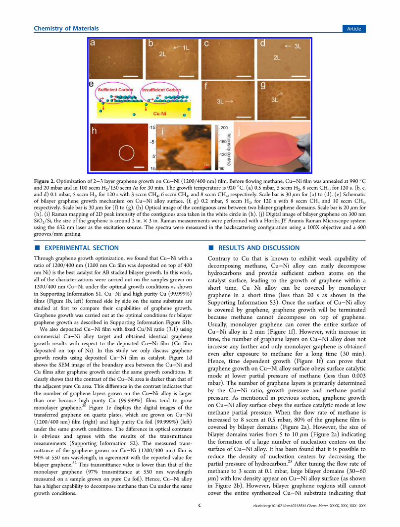
transport measurement is another reliable method to estimatethe stacking order of few layer (1−3 layer) graphene. Byapplying a vertical electrical field to few layer graphene withdifferent stacking modes and numbers of layers, the resistancesof graphene exhibit distinct behavior, which can be used toestimate the stacking order of few layer graphene.8 Grapheneareas are randomly selected and patterned by electron beamlithography. Over 50 dual gate devices were fabricated (Figure7a, details of device fabrication and device structure areincluded in the Supporting Information S7). All measurementswere carried out under ambient conditions. Figure 7b shows atwo-dimensional contour plot of the resistance of a bilayergraphene device as a function of top and bottom gate voltages,Vtg and Vbg, respectively. The resistance of bilayer graphene isalso illustrated in Figure 7c using the plot of Rtotal as a functionof Vtg for different fixed Vbg values. It can be observed that theresistance reaches the maximum value at the largest averagedisplacement fields, which is on the top left and bottom right ofFigure 7b, and on the left and right of Figure 7c, respectively.This behavior indicates that our bilayer graphene has an ABstacking order.9,14
The ON/OFF ratio (defined as the ratio of maximum tominimum resistance in the Vtg range of −5 to 5 V for a fixed Vds
and Vbg (Figure 7c)) of our bilayer graphene device is around10−15. We found that the ON/OFF ratio of the bilayergraphene device is strongly influenced by the sampletreatments. Before depositing the top dielectric layer, bakingthe device in high vacuum substantially enhanced the deviceperformance. Without vacuum treatment, the bilayer graphenedevice shows worse ON/OFF ratio (around 5−6) and theresistance tends to keep increasing at certain Vtg and Vbg in onedirection (Supporting Information S8). For trilayer graphene,the resistance evolution, which is shown in Figure 7d,e,decreases with increasing perpendicular electric field due to anoverlap between the conduction and valence bands that can becontrolled by an electric field, indicating that this trilayergraphene has ABA stacking order.36
Figure 5. Histogram of the distribution of (a) 2D/G ratio and (b)fwhm collected from the 3 in. × 3 in. bilayer graphene sample shownin Figure 2j.
Figure 6. (a, c) SAED patterns of AB stacked bilayer and trilayer graphene, respectively. (b, d) The corresponding intensity profiles (intensity vsdffraction vector k) collected along the white lines in (a) and (c), respectively (with zero corresponding to the top/bottom of the white lines). (e)HRTEM image of bilayer graphene; the inset fast Fourier transform (FFT) pattern indicates that the graphene is AB stacked. The TEM analysis wascarried out in Titan TEM at 200 KV.
Chemistry of Materials Article
dx.doi.org/10.1021/cm4021854 | Chem. Mater. XXXX, XXX, XXX−XXXF
The mobility of the bilayer and trilayer graphene could becalculated using the back gated FET devices as shown inSupporting Information S9. For bilayer and trilayer graphene,the electron mobility is around 2400−3450 cm2/(V·s) and500−1500 cm2/(V·s), respectively. These values are compara-ble to those of micromechanically cleaved bilayer and trilayergraphene (1500−4000 cm2/(V·s)),37 higher than that ofepitaxially grown bilayer graphene (550 cm2/(V·s)),26 andlower than our previously reported non-AB stacked CVDgrown bilayer graphene (5500 cm2/(V·s)).20
We found that the stacking order of the synthesizedgraphene is strongly influenced by the bulk Cu/Ni ratio andgrowth temperature. Figure 8a shows the yield of AB stackedgraphene as a function of bulk Cu/Ni ratio. With low Cuconcentration (less than 30 atom %) in bulk Cu/Ni, the yieldof AB stacked graphene is almost zero. Under such conditions,graphene growth behavior is similar to that in Ni (Supporting
Information S10) due to the high concentration of Ni, whichcan decompose much more methane and also dissolve morecarbon in the Cu−Ni alloy. Those dissolved carbon atoms willsegregate to the surface forming nonuniform few layergraphene layer-by-layer with each new layer formed belowthe existing layer(s) (as in few layer graphene growth mode onNi38).When bulk Cu concentration is in the range of 70−80 atom
%, Cu−Ni alloy exhibits high probability of growing AB stackedgraphene at 920 °C as shown in Figure 8a. When bulk Cuconcentration is in the range of 70−80 atom %, the surface Cuconcentration is about 95 atom % as shown in Figure 8a.Moreover, as shown in the previous sections, surface catalyticgraphene growth mode has been achieved at high surface Cuconcentrations in the low pressure CVD process. This indicatesthat many nucleation centers must form on the catalyst surface.The formation of the nucleation centers is confirmed by the
Figure 7. (a) Optical microscopy image of the fabricated dual gate graphene FET. (b, d) 2D Rtotal (the total channel resistance) as function of top-gate voltage (Vtg) and bottom-gate voltage (Vbg) of the representative bilayer and trilayer dual gate graphene FET devices, respectively. (c, e) Rtotal vsVtg at different fixed Vbg values of bilayer and trilayer graphene devices. The Vbg voltage varies from −30 to 15 V with a step of 5 V and from −40 to40 V with a step of 8 V for bilayer and trilayer graphene devices, respectively. (f) Statistics of the mobility of bilayer and trilayer graphene from 50back gated FET devices, respectively. References for exfoliated graphene (EG), CVD graphene, and chemically exfoliated graphene (CEG) are ref 37,ref 26, and ref 15, respectively. All of the referenced graphene are AB stacked graphene.
Figure 8. Optimization of graphene growth on Cu−Ni catalyst and element analysis. (a) The influence of Cu atom % in the Cu−Ni alloy on ABstacking yield. These Cu concentration values are obtained from the deposited Cu/Ni thickness before annealing and graphene growth. The redcurve shows the estimated Cu surface concentration as a function of the bulk Cu concentration in Cu−Ni alloy at 920 °C. (b) Effect of temperatureon the AB stacking yield, catalyst is Cu−Ni (1200/400 nm) film.
Chemistry of Materials Article
dx.doi.org/10.1021/cm4021854 | Chem. Mater. XXXX, XXX, XXX−XXXG
existence of individual bilayer graphene domains as shown inFigure 2a, b. On the other hand, the grown bilayer grapheneunder surface catalytic mode is all AB stacked (Figure 2d). Thisimplies that the nucleation centers of bilayer graphene must beAB stacked. Subsequently, the carbon atoms diffuse to the edgeof the nucleation centers and form a uniform bilayer graphenefilm, thereby preserving the stacking order.We also found that the yield of AB stacked bilayer graphene
decreases along with the increase of bulk Cu concentration(>80 atom %). At such a high bulk Cu concentration, surfacecatalytic graphene growth mode still dominates graphenegrowth on Cu−Ni alloy. However, the result of increasing bulkCu concentration beyond 80 atom % results in a correspondingincrease (>95 atom %) in surface Cu concentration (Figure 8a,red curve), which simultaneously decreases the hydrocarbondecomposition (due to lack of Ni) leading to lower carbonconcentration on the Cu−Ni alloy surface.Besides the Cu/Ni ratio, we also found that temperature can
significantly influence the yield of AB stacked graphene (Figure8b). Cu surface concentration is around 95 atom % for thetemperature in the range of 880−980 °C as shown inSupporting Information S11. When the temperature is in therange of 915−930 °C, grown graphene has an AB stackedconfiguration with yield of around 95−100%.This high yield can be attributed to the achievement of
surface catalytic graphene growth mode with a certain methanedecomposition rate. However, when the temperature is above930 °C, the AB stacked graphene yield gradually decreases from95% to 20% (at 980 °C). In addition, it is difficult to growuniform bilayer graphene at high temperatures (>930 °C). Thiscan be explained by the fact that high temperature will help thecatalyst to decompose more methane and many more carbonatoms will diffuse into the bulk resulting in carbon segregationand thereby decreasing the yield of AB stacked graphene.Although surface catalytic growth mode still occurs on part ofthe catalyst surface leading to the growth of some AB stackedgraphene, carbon atom segregation mode will graduallydominate the graphene formation mechanism along withincrease in the growth temperature. On the other hand, attemperatures less than 900 °C, Cu−Ni alloy tends to growmostly monolayer graphene with small few-layer domains dueto insufficient carbon sources. Thus, the AB stacked few layergraphene yield is low.Therefore, on the basis of the yield of AB stacked bilayer
graphene, for both Cu (or Ni) surface concentration andgrowth temperature, it can be concluded that achieving surfacecatalytic graphene growth mode and precise control of thesurface carbon concentration determines the formation ofuniform large scale AB stacked bilayer graphene. Tosummarize, the optimal growth condition for AB stackedbilayer graphene on Cu (1200 nm)/Ni (400 nm) is to flow 5sccm H2 and 8 sccm CH4 at 0.1 mbar and 920 °C for 120 safter an annealing at 20 mbar and 990 °C with 100 sccm H2/150 sccm Ar for 30 min.
■ CONCLUSIONSIn conclusion, we have demonstrated a reliable bottom-upmethod for large-area (3 in. × 3 in.) and high quality ABstacked bilayer graphene growth by engineering a bifunctionalsubstrate where the decomposition of hydrocarbons and thesurface diffusion induced growth are both tailored with theright combination of surface Cu concentration and temper-ature. It was found that achieving surface catalytic graphene
growth mode and precise control of the surface carbonconcentration are key factors determining the favorable growthkinetics for AB stacked bilayer graphene. After catalystengineering and growth parameter optimization, highly uniformAB stacked bilayer graphene or trilayer domains (30 μm × 30μm) can be grown on deposited Cu−Ni (1200/400 nm) filmon the wafer scale. The AB stacking order of synthesizedgraphene was confirmed by Raman spectra, TEM diffractionpattern, and dual gated FET measurements. The measuredmobility of the bilayer and trilayer graphene was extracted to beas high as 3450 cm2/(V·s) and 1500 cm2/(V·s), respectively,indicating comparable quality with respect to exfoliated bilayerand trilayer AB stacked graphene. Moreover, we demonstrateda large number (>50) of dual-gated field-effect transistors withrecord high ON to OFF current ratios (as high as 15)fabricated at random across the large-area bilayer CVDgraphene film, which further confirms the quality of oursynthesized graphene.
■ ASSOCIATED CONTENT*S Supporting Information(1) CVD system setup, growth parameters, and graphenetransfer process; (2) transmittance of monolayer and bilayergraphene; (3) time dependent graphene growth on Cu−Nifilm, Cu foil. and Ni film; (4) Raman spectra of AB stacked andnon-AB stacked bilayer and trilayer graphene; (5) XPS analysisof Cu−Ni and carbon composition in Cu−Ni alloy; (6) 2Dpeak fitting of AB stacked bilayer graphene; (7) dual-gategraphene FET fabrication process flow; (8) effect of doping onthe performance of bilayer graphene FET; (9) mobilitycalculation; (10) graphene growth on Ni rich and Cu richalloy; and (11) calculation of the Cu concentration on surfaceof Cu−Ni film. This material is available free of charge via theInternet at http://pubs.acs.org.
■ AUTHOR INFORMATIONCorresponding Author*E-mail: [email protected] ContributionsThe manuscript was written through contributions of allauthors.NotesThe authors declare no competing financial interest.
■ ACKNOWLEDGMENTSAll process steps for device fabrication were carried out usingthe Nanostructure Cleanroom Facility at the CaliforniaNanoSystems Institute and the Nanofabrication Facilities atUCSB - part of the National Nanotechnology InfrastructureNetwork. This work was supported by the National ScienceFoundation under Grant CCF-0811880 and by the U.S.Department of Energy (DOE) through the Bay AreaPhotovoltaic Consortium (BAPVC). The authors madeextensive use of the MRL Central Facilities at UCSB, whichare supported by the MRSEC Program of the NSF (underAward No. DMR 1121053), a member of the NSF-fundedMaterials Research Facilities Network (www.mrfn.org). P.M.A.acknowledges support from the Office of Naval Researchthrough the MURI program on graphene.
■ REFERENCES(1) Geim, A. K.; Novoselov, K. S. Nat. Mater. 2007, 6, 183.
Chemistry of Materials Article
dx.doi.org/10.1021/cm4021854 | Chem. Mater. XXXX, XXX, XXX−XXXH
(2) Freitag, M.; Chiu, H.-Y.; Steiner, M.; Perebeinos, V.; Avouris, P.Nat. Nanotechnol. 2010, 5, 497.(3) Li, H.; Xu, C.; Srivastava, N.; Banerjee, K. IEEE Trans. ElectronDevices 2009, 56, 1799.(4) Xu, C.; Li, H.; Banerjee, K. IEEE Trans. Electron Devices 2009, 56,1567.(5) Schwierz, F. Nat. Nanotechnol. 2010, 5, 487.(6) Han, M. Y.; Ozyilmaz, B.; Zhang, Y.; Kim, P. Phys. Rev. Lett. 2007,98, 206805.(7) Wang, X.; Ouyang, Y.; Li, X.; Wang, H.; Guo, J.; Dai, H. Phys.Rev. Lett. 2008, 100, 206803.(8) Lopes dos Santos, J.; Peres, N.; Castro Neto, A. Phys. Rev. Lett.2007, 99, 256802.(9) Zhang, Y.; Tang, T.-T.; Girit, C.; Hao, Z.; Martin, M. C.; Zettl,A.; Crommie, M. F.; Shen, Y. R.; Wang, F. Nature 2009, 459, 820.(10) Castro, E. V.; Novoselov, K.; Morozov, S.; Peres, N.; DosSantos, J. L.; Nilsson, J.; Guinea, F.; Geim, A.; Neto, A. C. Phys. Rev.Lett. 2007, 99, 216802.(11) Kosynkin, D. V.; Higginbotham, A. L.; Sinitskii, A.; Lomeda, J.R.; Dimiev, A.; Price, B. K.; Tour, J. M. Nature 2009, 458, 872.(12) Jiao, L.; Zhang, L.; Wang, X.; Diankov, G.; Dai, H. Nature 2009,458, 877.(13) Kuzmenko, A.; Crassee, I.; Van der Marel, D.; Blake, P.;Novoselov, K. Phys. Rev. B 2009, 80, 165406.(14) Xia, F.; Farmer, D. B.; Lin, Y.-m.; Avouris, P. Nano Lett. 2010,10, 715.(15) Chih-Jen, S.; Vijayaraghavan, A.; Krishnan, R.; Sharma, R.; Jae-Hee, H.; Moon-Ho, H.; Zhong, J.; Shangchao, L.; Paulus, G. L. C.;Reuel, N. F.; Qing Hua, W.; Blankschtein, D.; Strano, M. S. Nat.Nanotechnol. 2011, 6, 439.(16) Reina, A.; Jia, X.; Ho, J.; Nezich, D.; Son, H.; Bulovic, V.;Dresselhaus, M. S.; Kong, J. Nano Lett. 2008, 9, 30.(17) Liu, W.; Chung, C.-H.; Miao, C.-Q.; Wang, Y.-J.; Li, B.-Y.; Ruan,L.-Y.; Patel, K.; Park, Y.-J.; Woo, J.; Xie, Y.-H. Thin Solid Films 2010,518, S128.(18) Lee, S.; Lee, K.; Zhong, Z. Nano Lett. 2010, 11, 4702.(19) Robertson, A. W.; Warner, J. H. Nano Lett. 2011, 11, 1182.(20) Liu, W.; Li, H.; Xu, C.; Khatami, Y.; Banerjee, K. Carbon 2011,49, 4122.(21) Vlassiouk, I.; Regmi, M.; Fulvio, P.; Dai, S.; Datskos, P.; Eres,G.; Smirnov, S. ACS Nano 2011, 5, 6069.(22) Liu, L.; Zhou, H.; Cheng, R.; Yu, W.; Liu, Y.; Chen, Y.; Shaw, J.;Zhong, X.; Huang, Y.; Duan, X. ACS Nano 2012, 6, 8241.(23) Luo, Z.; Yu, T.; Shang, J.; Wang, Y.; Lim, S.; Liu, L.; Gurzadyan,G. G.; Shen, Z.; Lin, J. Adv. Funct. Mater. 2011, 21, 911.(24) Bhaviripudi, S.; Jia, X.; Dresselhaus, M. S.; Kong, J. Nano Lett.2010, 10, 4128.(25) Gao, L.; Ren, W.; Xu, H.; Jin, L.; Wang, Z.; Ma, T.; Ma, L.-P.;Zhang, Z.; Fu, Q.; Peng, L.-M. Nat. Commun. 2012, 3, 699.(26) Yan, K.; Peng, H.; Zhou, Y.; Li, H.; Liu, Z. Nano Lett. 2011, 11,1106.(27) Levendorf, M. P.; Ruiz-Vargas, C. S.; Garg, S.; Park, J. Nano Lett.2009, 9, 4479.(28) Chen, S.; Cai, W.; Piner, R. D.; Suk, J. W.; Wu, Y.; Ren, Y.;Kang, J.; Ruoff, R. S. Nano Lett. 2011, 11, 3519.(29) Liu, N.; Fu, L.; Dai, B.; Yan, K.; Liu, X.; Zhao, R.; Zhang, Y.; Liu,Z. Nano Lett. 2011, 11, 297.(30) Dalmon, J. J. Catal. 1979, 60 (2), 325.(31) Wandelt, K.; Brundle, C. Phys. Rev. Lett. 1981, 46, 1529.(32) Sun, Z.; Yan, Z.; Yao, J.; Beitler, E.; Zhu, Y.; Tour, J. M. Nature2010, 468, 549.(33) Kim, K.; Coh, S.; Tan, L. Z.; Regan, W.; Yuk, J. M.; Chatterjee,E.; Crommie, M.; Cohen, M. L.; Louie, S. G.; Zettl, A. Phys. Rev. Lett.2012, 108, 246103.(34) He, R.; Chung, T.-F.; Delaney, C.; Keiser, C.; Jauregui, L.;Shand, P. M.; Chancey, C.; Wang, Y.; Bao, J.; Chen, Y. P. Nano Lett.2013, 13, 3594.(35) Suh, Y.; Park, S.; Kim, M. Microsc. Microanal. 2009, 15 (S2),1168.
(36) Craciun, M. F.; Russo, S.; Yamamoto, M.; Oostinga, J. B.;Morpurgo, A. F.; Tarucha, S. Nat. Nanotechnol. 2009, 4, 383.(37) Nagashio, K.; Nishimura, T.; Kita, K.; Toriumi, A. Appl. Phys.Exp. 2009, 2, 025003.(38) Odahara, G.; Otani, S.; Oshima, C.; Suzuki, M.; Yasue, T.;Koshikawa, T. Surf. Sci. 2011, 605, 1095.
Chemistry of Materials Article
dx.doi.org/10.1021/cm4021854 | Chem. Mater. XXXX, XXX, XXX−XXXI


![Controllable Sliding Bearings and Controllable Lubrication ... · Review Controllable Sliding Bearings and Controllable ... or evolutionary [5], but it does not change the fact that](https://static.fdocuments.us/doc/165x107/5fc50df11ca4e1756528a85b/controllable-sliding-bearings-and-controllable-lubrication-review-controllable.jpg)