Control Plane Hardware Design for Optical Packet Switched ...
208
Control Plane Hardware Design for Optical Packet Switched Data Centre Networks Paris Andreades A dissertation submitted in partial fulfilment of the requirements for the degree of Doctor of Philosophy of University College London Optical Networks Group Department of Electronic and Electrical Engineering University College London November, 2019
Transcript of Control Plane Hardware Design for Optical Packet Switched ...

Control Plane Hardware Design forOptical Packet SwitchedData Centre Networks
Paris Andreades
A dissertation submitted in partial fulfilment
of the requirements for the degree of
Doctor of Philosophy
of
University College London
Optical Networks Group
Department of Electronic and Electrical Engineering
University College London
November, 2019

2
I, Paris Andreades, confirm that the work presented in this thesis is my own.
Where information has been derived from other sources, I confirm that this has been
indicated in the work.

Abstract
Optical packet switching for intra-data centre networks is key to addressing traffic
requirements. Photonic integration and wavelength division multiplexing (WDM)
can overcome bandwidth limits in switching systems. A promising technology
to build a nanosecond-reconfigurable photonic-integrated switch, compatible with
WDM, is the semiconductor optical amplifier (SOA). SOAs are typically used as
gating elements in a broadcast-and-select (B&S) configuration, to build an optical
crossbar switch. For larger-size switching, a three-stage Clos network, based on
crossbar nodes, is a viable architecture. However, the design of the switch control
plane, is one of the barriers to packet switching; it should run on packet timescales,
which becomes increasingly challenging as line rates get higher. The scheduler,
used for the allocation of switch paths, limits control clock speed. To this end,
the research contribution was the design of highly parallel hardware schedulers for
crossbar and Clos network switches. On a field-programmable gate array (FPGA),
the minimum scheduler clock period achieved was 5.0 ns and 5.4 ns, for a 32-port
crossbar and Clos switch, respectively. By using parallel path allocation modules,
one per Clos node, a minimum clock period of 7.0 ns was achieved, for a 256-port
switch. For scheduler application-specific integrated circuit (ASIC) synthesis, this
reduces to 2.0 ns; a record result enabling scalable packet switching. Furthermore,
the control plane was demonstrated experimentally. Moreover, a cycle-accurate
network emulator was developed to evaluate switch performance. Results showed a
switch saturation throughput at a traffic load 60% of capacity, with sub-microsecond
packet latency, for a 256-port Clos switch, outperforming state-of-the-art optical
packet switches.

Impact Statement
Optical packet switching is a viable solution to continue increasing the network
performance, in response to the traffic requirements inside a data centre. A major
challenge is the clock speed of the switch control plane. This has to be on packet
timescales, which keep decreasing as line rates keep increasing. The clock speed is
typically limited by the scheduler, responsible for the fair allocation of switch paths
and resolving any contention.
The impact of the research conducted is the contribution of a collection of
scheduler designs, for crossbar and Clos-network switches, optimised for ultra-low
clock period, to enable large-size packet switching. The critical path in the designs
is identified. The digital design techniques and Clos routing algorithms applied, for
highly parallel scheduling and reducing the critical path, were discussed in detail.
A record minimum clock period was reported, for a 256-port Clos scheduler.
Although focus is on optical packet switch scheduling, all scheduler designs
presented are applicable to electronic crossbar and Clos-network packet switches.
From a resource point of view, there is no difference in allocating and activating,
for example, an SOA gate in an optical crossbar or a multiplexer in an electronic
crossbar. The same scheduler digital design principles and techniques are applicable
to both switch types.
The control plane was verified experimentally and it was used to demonstrate
optical packet switching with ultra-low end-to-end packet latency. The experiment
quantified the control plane delay contributions and identified the critical path. It
also revealed the implications of asynchronous operation on the performance of the
switch. The significance of the scheduler clock period was highlighted.

Impact Statement 5
A cycle-accurate network emulator, with packet-level detail, was developed.
This enables researchers to accurately assess the flow control and routing algorithm
of a network of any architecture, under different traffic patterns, as a function of
traffic load and network size. Packet latency and network throughput, which are key
performance metrics, can be measured with this tool. Also, because the emulator is
developed in a hardware description language, key circuits such as network control
modules can be directly implemented on a hardware platform, after verification.

Acknowledgements
First and foremost, I would like to thank my supervisor, Dr Georgios Zervas, for
his invaluable advice and generosity. His expertise on computer networks has led
to stimulating discussions on the PhD topic. I am also thankful to my previous
supervisor, Dr Philip M. Watts, for my digital design knowledge and skills.
I am grateful to fellow Optical Interconnects PhD students and dear friends,
Mr Joshua Benjamin and Mr Kari Clark, for the collaborative discussions we had,
which have deepened my understanding on the research subject.
Over the years in the Optical Networks research group, I have made some great
friends, who helped make my time truly enjoyable and I am thankful for that. In
particular, Dr M. Sezer Erkilinc, Dr Gabriel Saavedra Mondaca, Dr Gabriele Liga,
Mr Boris Karanov and Mr Hui Yuan.
A special thanks goes to Miss Amna Fareed Asghar, who has always been by
my side, throughout my research journey, and made my life in London an incredible
experience. Thank you for being there for me during stressful times.
In addition, I would like to acknowledge my younger brother, Mr Christos
Andreades, for the numerous motivating conversations we had about the future that
lies ahead.
Last but not least, I would like to express my gratitude towards my parents, Mr
Antonis Andreades and Mrs Andrie Andreades. You have always been there for me
and helped me realise my dreams. Without you, I would not be where I am today.

Contents
1 Introduction 20
1.1 Research Problem . . . . . . . . . . . . . . . . . . . . . . . . . . . 23
1.2 Thesis Structure . . . . . . . . . . . . . . . . . . . . . . . . . . . . 25
1.3 Key Contributions . . . . . . . . . . . . . . . . . . . . . . . . . . . 26
1.4 List of Publications . . . . . . . . . . . . . . . . . . . . . . . . . . 28
2 Literature Review 30
2.1 Non-blocking Architectures . . . . . . . . . . . . . . . . . . . . . . 30
2.1.1 Crossbar . . . . . . . . . . . . . . . . . . . . . . . . . . . 30
2.1.2 Clos Network . . . . . . . . . . . . . . . . . . . . . . . . . 31
2.2 Data Centre Network Architectures . . . . . . . . . . . . . . . . . . 34
2.2.1 Hierarchical Tree . . . . . . . . . . . . . . . . . . . . . . . 34
2.2.2 Leaf-Spine . . . . . . . . . . . . . . . . . . . . . . . . . . 36
2.3 Electrical Network Scaling Limitations . . . . . . . . . . . . . . . . 37
2.3.1 Transmission Distance and Bandwidth . . . . . . . . . . . . 37
2.3.2 Bandwidth Density . . . . . . . . . . . . . . . . . . . . . . 38
2.3.3 Switch Capacity and Power Consumption . . . . . . . . . . 39
2.4 Optical Networks for Future Data Centres . . . . . . . . . . . . . . 40
2.4.1 Transmission Distance and Bandwidth . . . . . . . . . . . . 40
2.4.2 Bandwidth Density . . . . . . . . . . . . . . . . . . . . . . 43
2.4.3 Switch Capacity and Power Consumption . . . . . . . . . . 44
2.5 Scheduling . . . . . . . . . . . . . . . . . . . . . . . . . . . . . . 44
2.5.1 Arbitration . . . . . . . . . . . . . . . . . . . . . . . . . . 45

Contents 8
2.5.2 Allocation . . . . . . . . . . . . . . . . . . . . . . . . . . . 50
2.6 Optical Switching . . . . . . . . . . . . . . . . . . . . . . . . . . . 53
2.6.1 Technologies . . . . . . . . . . . . . . . . . . . . . . . . . 53
2.6.2 Technologies Review and Comparison . . . . . . . . . . . . 61
2.6.3 Architectures . . . . . . . . . . . . . . . . . . . . . . . . . 63
2.6.4 Architectures Review and Comparison . . . . . . . . . . . . 76
3 System Concept 81
3.1 Switch Application . . . . . . . . . . . . . . . . . . . . . . . . . . 81
3.2 Wavelength-striped Transmission . . . . . . . . . . . . . . . . . . . 82
3.3 Switch Architecture . . . . . . . . . . . . . . . . . . . . . . . . . . 83
3.4 Switch Routing . . . . . . . . . . . . . . . . . . . . . . . . . . . . 85
3.5 Flow Control . . . . . . . . . . . . . . . . . . . . . . . . . . . . . 86
3.6 Review and Comparison to Related Work . . . . . . . . . . . . . . 89
3.7 Tools and Methodology . . . . . . . . . . . . . . . . . . . . . . . . 92
4 Crossbar Scheduler Design 102
4.1 Baseline Scheduler Design . . . . . . . . . . . . . . . . . . . . . . 102
4.1.1 Network Emulation Results . . . . . . . . . . . . . . . . . 106
4.1.2 Hardware Implementation . . . . . . . . . . . . . . . . . . 110
4.2 Pipeline Scheduler Design . . . . . . . . . . . . . . . . . . . . . . 115
4.2.1 Network Emulation Results . . . . . . . . . . . . . . . . . 117
4.2.2 Hardware Implementation . . . . . . . . . . . . . . . . . . 120
4.2.3 Crossbar Scheduler Comparison . . . . . . . . . . . . . . . 124
4.3 Summary . . . . . . . . . . . . . . . . . . . . . . . . . . . . . . . 126
5 Clos Switch Scheduler Design 128
5.1 Global Scheduler Design . . . . . . . . . . . . . . . . . . . . . . . 129
5.1.1 Network Emulation Results . . . . . . . . . . . . . . . . . 131
5.1.2 Hardware Implementation . . . . . . . . . . . . . . . . . . 133
5.2 Modular Scheduler Design . . . . . . . . . . . . . . . . . . . . . . 135
5.2.1 Clos Routing . . . . . . . . . . . . . . . . . . . . . . . . . 136

Contents 9
5.2.2 Scheduler Hardware Modules . . . . . . . . . . . . . . . . 137
5.2.3 Network Emulation Results . . . . . . . . . . . . . . . . . 148
5.2.4 Hardware Implementation . . . . . . . . . . . . . . . . . . 149
5.2.5 Switch Design Comparison . . . . . . . . . . . . . . . . . 154
5.3 Summary . . . . . . . . . . . . . . . . . . . . . . . . . . . . . . . 159
6 Experimental Demonstration 162
6.1 Control Plane Components . . . . . . . . . . . . . . . . . . . . . . 162
6.1.1 Server Network Interface . . . . . . . . . . . . . . . . . . . 162
6.1.2 Switch Scheduler . . . . . . . . . . . . . . . . . . . . . . . 163
6.2 Experimental Setup . . . . . . . . . . . . . . . . . . . . . . . . . . 166
6.3 Experimental Demonstration and Results . . . . . . . . . . . . . . 169
6.3.1 Scenario A . . . . . . . . . . . . . . . . . . . . . . . . . . 169
6.3.2 Scenario B . . . . . . . . . . . . . . . . . . . . . . . . . . 172
6.3.3 Asynchronous Control Plane Limitations . . . . . . . . . . 175
6.4 Balanced Pipeline Scheduler Design . . . . . . . . . . . . . . . . . 175
6.5 Network Emulation Results . . . . . . . . . . . . . . . . . . . . . . 177
6.6 Summary . . . . . . . . . . . . . . . . . . . . . . . . . . . . . . . 179
7 Conclusion & Future Work 182
7.1 Conclusion . . . . . . . . . . . . . . . . . . . . . . . . . . . . . . 182
7.2 Future Work . . . . . . . . . . . . . . . . . . . . . . . . . . . . . . 190
Bibliography 194

List of Figures
1.1 A hierarchical tree network in traditional data centres. . . . . . . . . 21
1.2 A leaf-spine network in current data centres. . . . . . . . . . . . . . 22
2.1 An N x N crossbar conceptual model. . . . . . . . . . . . . . . . . 31
2.2 A three-stage (m,n,r) Clos network. . . . . . . . . . . . . . . . . . 32
2.3 A (2,2,4) Clos network with two (2,2,2) Clos networks used as 4x4
central modules. This is also referred to as an 8x8 Benes network
due to composition using only 2x2 switch modules. . . . . . . . . . 34
2.4 A traditional multi-rooted three-tier data centre network topology.
Switch size and port capacity increase from access to core tiers. . . 35
2.5 The Leaf-Spine architecture. It is a Clos network folded along the
middle and rotated by 90 degrees. . . . . . . . . . . . . . . . . . . 36
2.6 Electrical link cross-section showing alternating current density dis-
tribution at high data rates. Current flows mainly within a depth δ
from the link’s outer edge or “skin”. This phenomenon is known as
the skin effect. . . . . . . . . . . . . . . . . . . . . . . . . . . . . . 37
2.7 On-chip wire model: (a) Wire cross-section and (b) The π model
for wire delay estimation. . . . . . . . . . . . . . . . . . . . . . . . 39
2.8 Optical power loss in silica single-mode fibre for different wave-
lengths. . . . . . . . . . . . . . . . . . . . . . . . . . . . . . . . . 41
2.9 Wavelength-division multiplexing (WDM). . . . . . . . . . . . . . 42
2.10 A bit cell for a variable priority arbiter. . . . . . . . . . . . . . . . . 45
2.11 A variable priority arbiter. . . . . . . . . . . . . . . . . . . . . . . 46
2.12 A variable priority arbiter optimised for hardware implementation. . 47

List of Figures 11
2.13 Round-robin priority generator. (a) A one-bit slice and (b) An n-bit
priority generator. . . . . . . . . . . . . . . . . . . . . . . . . . . . 49
2.14 A 2×4 input-first separable allocator. . . . . . . . . . . . . . . . . 51
2.15 A 2×4 output-first separable allocator. . . . . . . . . . . . . . . . . 52
2.16 Optical switch operation: (a) space switching and (b) wavelength
routing. . . . . . . . . . . . . . . . . . . . . . . . . . . . . . . . . 54
2.17 A 12× 12 Data Vortex with C = 3, H = 4 and A = 3. Module
connectivity shown from (a) top view and (b) side view. Module
coordinates are (c,h,a), where 0 ≤ c ≤ C− 1, 0 ≤ h ≤ H − 1, 0 ≤
a≤ A−1. . . . . . . . . . . . . . . . . . . . . . . . . . . . . . . . 66
2.18 A 2× 2 Data Vortex SOA-based B&S module. Header valid (V)
and address (A) bits are recovered to make routing decisions. Con-
trol logic turns SOAs “on”/“off”, based on address bit and input
deflection signal, and asserts output deflection signal, if necessary.
Deflection input/output signals shown in red. . . . . . . . . . . . . 67
2.19 An 8×8 binary butterfly network and destination-tag routing from
source 5 to destination 2. The destination address in binary is 210 =
0102 and selects the route at each network stage as up (0), down (1),
up (0). Regardless of the source, the pattern 010 always routes to
destination 5. This is valid for all possible destinations. . . . . . . . 68
2.20 A 2× 2 SPINet SOA-based B&S module. Header valid (V) and
address (A) bits are recovered to make routing decisions. Control
logic performs routing-aware output port allocation and turns SOAs
“on”/“off”. . . . . . . . . . . . . . . . . . . . . . . . . . . . . . . . 69
2.21 An N×N OPSquare switch. It is based on a parallel modular archi-
tecture with distributed control. . . . . . . . . . . . . . . . . . . . . 72
2.22 An N × N AWGR-based LION switch. The switch supports
all-optical token (AO-TOKEN)-based transmission and all-optical
negative acknowledgement (AO-NACK)-based re-transmission to
avoid packet loss. . . . . . . . . . . . . . . . . . . . . . . . . . . . 74

List of Figures 12
3.1 Proposed data centre network concept. Input-buffered optical top-
of-rack (ToR) switch reduces minimum packet latency and avoids
packet loss. A Clos network is a possible switch architecture.
A dedicated scheduler reconfigures the switch in nanoseconds.
Colour-coded in grey/black for electronic/electrical components
and in blue for optical components. . . . . . . . . . . . . . . . . . . 82
3.2 Packet transmission in (a) serial format and (b) wavelength-parallel
format. . . . . . . . . . . . . . . . . . . . . . . . . . . . . . . . . . 83
3.3 Clos module architecture using parallel 2× 2 SOA-based B&S
switch elements. The fundamental (a) 2×2 switch element is used
to build (b) a 4×4 module. An 8×8 module is built using the 4×4
module, and every twofold increase in size is implemented as such,
recursively around the 2×2 base element. . . . . . . . . . . . . . . 84
3.4 Switch architecture comparison. . . . . . . . . . . . . . . . . . . . 85
3.5 Proposed system concept. . . . . . . . . . . . . . . . . . . . . . . . 86
3.6 Control delay comparison for two flow control methods: (a) non-
speculative, (b) speculative - successful allocation and (c) specula-
tive - failed allocation. . . . . . . . . . . . . . . . . . . . . . . . . 87
3.7 Network emulation setup includes N packets sources, the N ×N
network under test and the packet sink. The network module ver-
ifies control and data plane functionality and adds delays to accu-
rately model the system concept. Once performance is evaluated,
the scheduler is either implemented on an FPGA or synthesised as
an ASIC. . . . . . . . . . . . . . . . . . . . . . . . . . . . . . . . 94
3.8 Behaviour of a Bernoulli process injecting packets at a rate rp over
time. The expected injection period is E(Tp) = 1/rp. . . . . . . . . 96
4.1 Scheduler design for an N×N crossbar. There are two critical paths
in the design, depending on N, shown in red. . . . . . . . . . . . . . 103
4.2 Average switch throughput vs. input traffic load, under Bernoulli
traffic. . . . . . . . . . . . . . . . . . . . . . . . . . . . . . . . . . 106

List of Figures 13
4.3 Minimum switch buffer size vs. input traffic load: (a) 4×4 crossbar,
(b) 8×8 crossbar, (c) 16×16 crossbar and (d) 32×32 crossbar. The
crossbar is under control of the baseline scheduler. . . . . . . . . . 108
4.4 Average end-to-end packet latency vs. input traffic load, for dif-
ferent switch sizes. Network model assumes 3 clock cycles prop-
agation delay to and from the switch, for both optical and electri-
cal links. Packets are 1 clock cycle long and injected based on a
Bernoulli process. . . . . . . . . . . . . . . . . . . . . . . . . . . . 109
4.5 Cumulative distribution of the packet end-to-end latency at (a) 25%,
(b) 50% and (c) 75% input traffic loads for different switch sizes.
The Network model assumes SOA-based crossbar with a 2 m link
distance to every connected source and destination. Packets are
64 B, wavelength-striped at 4× 100 Gb/s and injected based on a
Bernoulli process. . . . . . . . . . . . . . . . . . . . . . . . . . . . 113
4.6 Packet end-to-end average latency vs. input traffic load, for dif-
ferent switch sizes. Network model assumes SOA-based crossbar
with a 2 m link distance to every connected source and destination.
Packets are 64 B, wavelength-striped at 4× 100 Gb/s and injected
based on a Bernoulli process. . . . . . . . . . . . . . . . . . . . . . 114
4.7 Scheduler design parallelism: (a) spatial and (b) temporal. . . . . . 115
4.8 Scheduler design with 2-stage pipeline for an N×N crossbar. The
critical path in the design is shown in red. . . . . . . . . . . . . . . 116
4.9 Average switch throughput vs. input traffic load, under Bernoulli
traffic. . . . . . . . . . . . . . . . . . . . . . . . . . . . . . . . . . 118
4.10 Minimum switch buffer size vs. input traffic load: (a) 4×4 crossbar,
(b) 8×8 crossbar, (c) 16×16 crossbar and (d) 32×32 crossbar. The
crossbar is under control of the pipeline scheduler. . . . . . . . . . . 119

List of Figures 14
4.11 Average end-to-end packet latency vs. input traffic load, for dif-
ferent switch sizes. Network model assumes 3 clock cycles prop-
agation delay to and from the switch, for both optical and electri-
cal links. Packets are 1 clock cycle long and injected based on a
Bernoulli process. . . . . . . . . . . . . . . . . . . . . . . . . . . . 119
4.12 Cumulative distribution of the packet end-to-end latency at (a) 25%,
(b) 50% and (c) 75% input traffic loads, for different switch sizes.
The network model assumes SOA-based crossbar with a 2 m link
distance to every connected source and destination. Packets are
64 B, wavelength-striped at 4× 100 Gb/s and injected based on a
Bernoulli process. . . . . . . . . . . . . . . . . . . . . . . . . . . . 123
4.13 Average end-to-end packet latency vs. input traffic load, for differ-
ent switch sizes. The network model assumes SOA-based crossbar
with a 2 m link distance to every connected source and destination.
Packets are 64 B, wavelength-striped at 4× 100 Gb/s and injected
based on a Bernoulli process. . . . . . . . . . . . . . . . . . . . . . 124
5.1 Scheduler design with 3-stage pipeline for an N×N Clos switch.
The critical path in the design is shown in red. . . . . . . . . . . . . 130
5.2 Average switch throughput vs. input traffic load, for a 32× 32
switch built in different architectures, under Bernoulli traffic. . . . . 132
5.3 Average end-to-end packet latency vs input traffic load, for 32×
32 switches in different architecture and scheduler implementation
on the Xilinx Virtex-7 XC7VX690T FPGA. The network model
assumes SOA-based Clos switch with a 2 m link distance to every
connected source and destination. Packets are 64 B, wavelength-
striped at 4×100 Gb/s and injected based on a Bernoulli process. . 135
5.4 An (m,n,r) Clos network with strictly non-blocking modules. The
proposed routing scheme, for m = n = r Clos networks, assigns fixed
paths to eliminate routing overhead and avoid contention at the cen-
tral modules, simplifying the scheduler design and reducing its delay. 136

List of Figures 15
5.5 Scheduler design with 3-stage pipeline for an N×N Clos switch, in
which m = n = r =√
N. The critical path in the design is in the 1st
pipeline stage, through the iSLIP allocator. . . . . . . . . . . . . . . 138
5.6 Clos switch scheduler design in a planar-modular visualisation.
Planes operate independently and in parallel to allocate paths based
on output module (OM) and output port (OP) arbitration for the
Clos input and output modules. The switch configuration module
reconfigures the switch based on the allocation grants from both
planes. . . . . . . . . . . . . . . . . . . . . . . . . . . . . . . . . . 138
5.7 Output module allocator design for new packets. The critical path
in the design is shown in red. Tags A and B are for cross-reference
with Fig. 5.8. . . . . . . . . . . . . . . . . . . . . . . . . . . . . . 140
5.8 Example request processing for new packets by the output module
allocator, for the 2nd input module in a (4,4,4) Clos switch. Binary
matrices are tagged for cross-reference with the digital design in
Fig. 5.7. . . . . . . . . . . . . . . . . . . . . . . . . . . . . . . . . 140
5.9 Output module allocator design for switch VOQ packets. The crit-
ical path in the design is shown in red. Tags A-E are for cross-
reference with Fig. 5.10. . . . . . . . . . . . . . . . . . . . . . . . 142
5.10 Example request processing for switch VOQ packets by the output
module allocator, for the 2nd input module in a (4,4,4) Clos switch.
Binary matrices are tagged for cross-reference with the digital de-
sign in Fig. 5.9. . . . . . . . . . . . . . . . . . . . . . . . . . . . . 142
5.11 Output port allocator design. The same design is used for new pack-
ets and for switch VOQ packets. The critical path in the design is
shown in red. Tags A-C are for cross-reference with Fig. 5.12. . . . 144
5.12 Example request processing by the output port allocator for the 2nd
output module, in a (4,4,4) Clos switch. Binary matrices are tagged
for cross-reference with the digital design in Fig. 5.11. . . . . . . . 144

List of Figures 16
5.13 Switch configuration module design. Blue-coded logic blocks are
for VOQ packets and rest blocks for new packets. The critical path
in the design is marked in red. . . . . . . . . . . . . . . . . . . . . 147
5.14 Average switch throughput vs input traffic load, under Bernoulli
traffic. . . . . . . . . . . . . . . . . . . . . . . . . . . . . . . . . . 148
5.15 Minimum switch virtual output queue (VOQ) size vs. input traf-
fic load: (a) 16× 16 Clos switch, (b) 64× 64 Clos switch and (c)
256× 256 Clos switch. All VOQs at every switch input port are
considered, to ensure no packet loss. . . . . . . . . . . . . . . . . . 149
5.16 Cumulative distribution of the packet end-to-end latency at (a) 25%,
(b) 50% and (c) 75% input traffic loads, for different size Clos
switches, and ASIC scheduler. Network model assumes SOA-based
Clos switch with a 2 m link distance to every source and destination.
Packets are 64 B, wavelength-striped at 8× 100 Gb/s and injected
based on a Bernoulli process. . . . . . . . . . . . . . . . . . . . . . 153
5.17 Average end-to-end latency vs. input traffic load, for different size
Clos switches, and ASIC scheduler. Network model assumes SOA-
based Clos switch with a 2 m link distance to every source and
destination. Packets are 64 B, wavelength-striped at 8× 100 Gb/s
and injected based on a Bernoulli process. . . . . . . . . . . . . . . 154
5.18 Switch average throughput vs. input traffic load, for different switch
designs, under Bernoulli traffic. . . . . . . . . . . . . . . . . . . . . 157
5.19 Average end-to-end packet latency vs. input traffic load, for differ-
ent switch designs. Clos-MDLR/GLBL latency is based on sched-
uler implementation on the Virtex-7 XC7V690T FPGA board. The
network model assumes a 2 m link distance to every source and des-
tination. Packets are 64 B and injected based on a Bernoulli process. 158
6.1 Scheduler design with 2-stage pipeline for an N × N crossbar
switch. Critical path shown in red. . . . . . . . . . . . . . . . . . . 164

List of Figures 17
6.2 The experimental setup. Control path and data path latency con-
tributions and the minimum end-to-end latency are marked on the
figure. Oscilloscope probes D0-D7 are placed along the data path.
Xilinx Integrated Logic Analyzer (ILA) probes C0-C6 are imple-
mented onto the scheduler FPGA board. . . . . . . . . . . . . . . . 166
6.3 Experimental scenarios: a) switching packets from an input port to
two output ports and b) switching packets from two input ports to
an output port. . . . . . . . . . . . . . . . . . . . . . . . . . . . . . 169
6.4 Scheduler shown allocating the two switch output ports in turn, one
at a time, to the requesting server network interface. Traces are
labelled according to the probe placement shown in Fig. 6.2. Each
subdivision is 1Tscheduler. . . . . . . . . . . . . . . . . . . . . . . . 170
6.5 Data path from a server network interface to the two switch out-
put ports. Traces are labelled according to the probe placement
shown in Fig. 6.2. The minimum end-to-end latency measurement
is marked in this Figure. . . . . . . . . . . . . . . . . . . . . . . . 171
6.6 Effect of request synchronisation uncertainty on the switch config-
uration. The switch configuration pulse timing is captured using a
5-second persistence on the oscilloscope. The speculatively trans-
mitted packet is shown arriving at the switch SOA at the right time. . 172
6.7 Scheduler shown allocating one switch output port to the two re-
questing server network interfaces, one at a time. Traces are la-
belled according to the probe placement shown in Fig. 6.2. Each
subdivision is 1Tscheduler. . . . . . . . . . . . . . . . . . . . . . . . 173
6.8 Data path from the two server network interfaces to the first switch
output port. Traces are labelled according to the probe placement
shown in Fig. 6.2. The minimum end-to-end latency and packet
spacing measurements are marked in this Figure. . . . . . . . . . . 174
6.9 Minimum clock period vs. switch size, for two crossbar scheduler
designs, implemented on the Xilinx Kintex-7 XC7K325T FPGA. . . 176

List of Figures 18
6.10 Cumulative distribution function of packet end-to-end latency, at
50% input traffic load, for two different scheduler designs imple-
mented on the Xilinx Kintex-7 XC7K325T FPGA. The network
model assumes an SOA-based, 32×32 crossbar switch with a 2 m
link distance to every connected source and destination. Packets are
64 bytes, wavelength-striped at 8×10 Gb/s and injected based on a
Bernoulli process. . . . . . . . . . . . . . . . . . . . . . . . . . . . 179
6.11 Average end-to-end packet latency vs. input traffic load, for
two different scheduler designs, implemented on Xilinx Kintex-7
XC7K325T FPGA. The network model assumes an SOA-based,
32×32 crossbar switch with a 2 m link distance to every connected
source and destination. Packets are 64 bytes, wavelength-striped at
8×10 Gb/s and injected based on a Bernoulli process. . . . . . . . 179

List of Tables
2.1 Switching Technologies Comparison . . . . . . . . . . . . . . . . . 61
2.2 Flow Control Comparison for Different Switch Architectures . . . . 79
3.1 Parameters for Network Emulation . . . . . . . . . . . . . . . . . . 97
3.2 Parameters for Absolute Packet Latency Calculation. . . . . . . . . 100
4.1 Throughput Saturation Traffic Load vs. Switch Size. . . . . . . . . 107
4.2 Xilinx Virtex-7 XC7VX690T FPGA Timing and Utilisation Results. 110
4.3 Minimum End-to-End Packet Latency vs. Switch Size. . . . . . . . 112
4.4 Comparison of Throughput Saturation Traffic Load vs. Switch Size. 118
4.5 Xilinx Virtex-7 XC7VX690T FPGA Timing and Utilisation Results. 120
4.6 Minimum End-to-End Packet Latency vs. Switch Size. . . . . . . . 121
4.7 Minimum Clock Period for Different Scheduler Designs. . . . . . . 125
5.1 Throughput Saturation Traffic Load vs. 32×32 Switch Architecture. 133
5.2 Xilinx Virtex-7 XC7V690T FPGA Timing and Utilisation Results. . 133
5.3 Minimum Packet Latency vs. 32×32 Switch Architecture. . . . . . 134
5.4 Scheduler Modules Minimum Clock Period for ASIC Synthesis. . . 150
5.5 Scheduler Minimum Clock Period for FPGA Implementation. . . . 151
5.6 Minimum End-to-End Packet Latency vs. Switch Size. . . . . . . . 152
5.7 Scheduling Comparison . . . . . . . . . . . . . . . . . . . . . . . . 155
6.1 Parameters for Network Emulation. . . . . . . . . . . . . . . . . . 178

Chapter 1
Introduction
The ever increasing Internet traffic is dominated by data centre traffic, which is
projected to reach 20.6 zettabytes per year by 2021 [1]. Data centre traffic can be
divided into three main types: (a) traffic between data centres and users, (b) traffic
between data centres and (c) traffic within data centres. The latter accounts for more
than 70% of the data centre traffic and it is exchanged between network servers.
It is commonly known as East-West traffic, as opposed to the North-South traffic
which enters and exits the network, in traditional data centres. The East-West traffic
is driven by a number of technological trends. The growth of cloud computing
and virtualisation has led to servers running multiple virtual workloads, which are
commonly migrated from one server to another. Storage replication is also used to
a great extend, to ensure business continuity, having a significant contribution to
the inter-server traffic. Furthermore, new data centre applications rely on multiple
workloads distributed to different servers to run in parallel, thus generating traffic
between servers [1, 2].
The increasing East-West traffic has caused a shift in the data centre network
topology, due to stringent bandwidth and latency requirements. In the traditional
data centre, network switches were arranged in a tree topology with a three-layer
hierarchy, as illustrated in Fig. 1.1. A rack of servers at the network edge connected
to a top-of-rack (ToR) switch in the access layer. Switches in the aggregation layer
would then interconnect the racks. Finally, switches in the core layer were used
to interconnect aggregation switches, in order to increase the network size and the

21
ToR
Ag
gre
ga
tio
nA
cce
ss
Co
reS
erv
ers
Figure 1.1: A hierarchical tree network in traditional data centres.
performance. The switch port count and bit rate would be higher moving from the
access to the core layer, to support the higher volume of traffic in the upper layers.
To reduce network cost, over-subscription was often used at the network layers.
This refers to reducing the total uplink bandwidth with respect to the total downlink
bandwidth. This architectural model, although it catered to North-South traffic, is
not well suited for the East-West traffic exhibited in today’s data centres. Traffic
routed over different paths may traverse a different number of switches, leading to
unpredictable latency. Moreover, the high over-subscription ratios that are typically
used, would limit server throughput.
Small-scale data centre networks are now built in the leaf-spine topology [1, 3],
illustrated in Fig. 1.2. Compared to the traditional hierarchical tree, this topology is
flatter as it consists of only two layers; the leaf layer, in which the ToR switches lie,
and the spine, which interconnects the ToR switches [4]. Also, paths are equidistant,
in terms of number of hops, with servers in different racks experiencing only a three-
hop latency. Therefore, the minimum inter-server latency is low and predictable,

22
ToR
Sp
ine
Le
af
Se
rve
rs
Figure 1.2: A leaf-spine network in current data centres.
which favours East-West traffic [5]. Furthermore, every leaf (or ToR) switch is
connected to a spine switch and vice versa. Hence, in theory, no over-subscription
is applied, delivering full bisection bandwidth for the server communication. Also,
commodity switches can be deployed across the entire architecture, giving a more
cost-effective solution than the hierarchical tree model [6].
The electrical data centre interconnect, however, runs into physical limitations,
as the requirements on network size and bandwidth continue to increase. Due to
frequency-dependent losses, the length of an electrical link is limited as the bit rate
increases [7]. At 10 Gb/s, the transmission distance of copper transmission lines
is typically no longer than 10 m, to avoid signal distortion [8]. The bandwidth
of an electronic switch is also limited. The number of high-speed pins, available
on the switch chip, or the number of connectors fitting on a rack unit front panel,
limit the switched bandwidth [9]. The electronic switch design, as well as its power
consumption, are bit rate-dependent. An electronic switch dissipates energy with
every bit transition, thus consumes power proportional to the bit rate [10, 11, 12].
Optical interconnects, for intra-data centre networking, is an inevitable next
step for sustainable performance increase. A key optical technology, to significantly
increase bit rate, is wavelength-division multiplexing (WDM) [13]. It exploits the

1.1. Research Problem 23
very high bandwidth of an optical waveguide, such as fibre, to multiplex together k
independent data streams, modulated on dedicated wavelengths, that can propagate
simultaneously. The low loss and high bandwidth (through WDM) of an optical
fibre, overcomes the bit rate-distance limitation of electrical transmission lines and
allows for a low energy per bit to be achieved. In fact, optical fibre is already in
use in data centres, for point-to-point connectivity between switches [3, 14]. The
switches, however, are still electronic, which creates a bandwidth bottleneck and
limits energy efficiency. Optical switching is the sensible way forward. Integrated
photonics that use WDM, is a viable solution to overcome the pin and front panel
connector count limitations, and continue increasing the switched bandwidth. The
building blocks of an optical switch are transparent to the data bit rate. Thus, (a)
the switch design does not have to change, as bit rates continue to increase and (b)
the power consumed is independent of the switched bandwidth. Optical switching
is therefore a key enabler for network scalability.
Depending on the building block technology, the reconfiguration time of an
optical switch, varies from milliseconds to nanoseconds. Switches built as micro-
electro-mechanical systems or based on piezoelectric beam steering technology, are
already commercially available [15, 16]. Their high port count (100s of ports) and
low loss allow building a large data centre network, without any signal degradation
issues. However, these technologies limit the switch reconfiguration time to 10s of
milliseconds, suitable only for circuit switching. Several optical circuit-switched
network architectures have been proposed, based on such switches applied at the
network core, to handle high-volume traffic. Notable examples are the RotorNet
[17], Helios [8] and c-Through [18] architectures. Nevertheless, electronic packet
switching is still needed to handle small-size traffic or traffic that is bursty and
rapidly changing [19].
1.1 Research Problem
Optical packet switching is an attractive alternative. The capability of switching on
a per packet basis means that this solution can be widely deployed in the network,

1.1. Research Problem 24
in any hierarchy layer, without any limitations on the traffic stability or volume.
To support packet switching, the switch needs to be reconfigurable in nanoseconds.
A suitable technology is the semiconductor optical amplifier (SOA), used as an
optical gate, with switching transients of the order of 100 ps [20]. SOA-based
optical switch prototypes, such as the OPSquare [21], SPINet [11], OSMOSIS [12]
and Data Vortex [22], have been demonstrated experimentally. They all use SOA
gates in a broadcast-and-select configuration to build crossbar switching modules.
The modules are then used in a multi-stage architecture to scale the switch size.
A switch built entirely as a photonic-integrated circuit (PIC), is a practical
approach to cost- and energy-effective switching [9, 11]. Photonic-integrated packet
switches have been demonstrated based on SOA [23], Mach-Zehnder interferometer
(MZI) [24] and micro-ring resonator (MRR) [25] technologies. Network scalability
is limited by optical loss, crosstalk and noise accumulated per optical switch. The
inherent amplification of an SOA compensates for loss and, when deactivated, it
strongly suppresses crosstalk, making it an attractive technology. A switch built by
arranging SOA-based crossbar modules in a three-stage Clos network [26] topology,
has been shown viable at least up to a 64× 64 size, with a low level of noise [23].
An optical switch of this size can replace the currently electronic ToR switch in
the leaf layer (Fig. 1.2), accommodating sufficient optical links to interconnect a
rack of servers to the electronic switches in the core layer. In the resulting data
centre network, the most distant servers communicate with a minimum latency of
two hops; one hop from the source server to a core switch and another hop to the
destination server.
Despite the demonstration of nanosecond-reconfigurable photonic-integrated
switch architectures, optical packet switching is not yet employed in data centres.
The main impediments are the lack of practical random-access memory and limited
optical signal processing capabilities. A more pressing challenge, in optical packet
switch design, is the speed of the accompanying control plane. The control plane
implements the switch’s flow control; the allocation of switch resources, such as
output ports, also referred to as switch scheduling. Scheduling needs to be executed

1.2. Thesis Structure 25
on packet timescales. However, as the line rate keeps increasing, the packet duration
gets smaller which places stringent requirements on scheduling delay. To maintain
a low scheduling delay, as the switch size increases, is another challenge.
To this end, the research conducted and described in the thesis addresses the
scheduling problem; the design of parallel hardware schedulers for nanosecond
crossbar and Clos switch scheduling. The focus is to achieve ultra-low minimum
packet latency, which is particularly important for small-size packets, but also to
achieve a high switch throughput as the input traffic load is increased. The aim is
to deliver scalable optical packet switching to replace electronic switches, at least
at the leaf network layer, for future data centres. The scheduler is part of a novel
switch system concept that is proposed, which uses electronics for buffering and
processing and optics for low latency and high bandwidth packet switching.
1.2 Thesis StructureThe remainder of the thesis is structured as follows:
Chapter 2 reviews the literature to set the foundation on the thesis topic. The
target data centre architecture is presented and its performance limitations
due to the currently electrical interconnect, are discussed. Optical networking
for sustainable performance increase is argued. The significance and design
of resource allocation circuits, for packet switch scheduling, is discussed.
Optical switch technologies and demonstrated prototypes are compared.
Chapter 3 introduces the proposed system concept, covering the design of the
network interface, at every node, and the switch design, which addresses the
internal architecture, routing method and flow control. The proposed system
is compared to the other switch designs reviewed in Chapter 2. The tools
and methodology to implement the switch control plane and assess switch
performance, are described. This includes the development details of a cycle-
accurate network emulator with packet-level accuracy.
Chapter 4 presents the register-transfer level (RTL) design of a nanosecond
scheduler, for crossbar switches. The design has been optimised for clock

1.3. Key Contributions 26
speed using digital design techniques for parallelism. The crossbar scheduler
is implemented on hardware to measure the minimum clock period and assess
control plane scaling. Switch average throughput and packet latency, under
scheduler control, are measured in the network emulator.
Chapter 5 focuses on the size scalability of the proposed switching system.
The RTL designs of two highly-parallel schedulers, for switches built in a
Clos network topology, are presented. Routing algorithms, executable in a
single scheduler clock period, are applied. Clock period results for scheduler
synthesis as an application-specific integrated circuit (ASIC) are presented,
to verify scalability. The Clos switch, under control of either scheduler, is
compared to the reviewed designs in Chapter 2, in terms of scheduling delay,
average packet latency and throughput. The Clos scheduler designs have been
published in [27, 28].
Chapter 6 verifies experimentally the proposed system concept. A proof-
of-concept control plane demonstrator is built and used to showcase optical
packet switching. The improvement in switch performance, under control
of the optimised crossbar scheduler, presented in Chapter 4, is quantified.
The performance implications of using an asynchronous control plane are
discussed. The experimental demonstration has been published in [29, 30].
Chapter 7 draws conclusions based on conducted research and the results
obtained. Potential research directions, as part of future work, are suggested.
1.3 Key ContributionsAs a result of the work conducted, specialised tooling has been developed and a
number of contributions to the research field have been made. The key contributions
are listed below:
• An entire network emulator has been developed for control plane verification
and performance evaluation of the network under test, with a packet level of
detail. This includes traffic sources, network interfaces, a switch time model

1.3. Key Contributions 27
and the switch scheduler. All these network components are implemented as
hardware modules, developed in SystemVerilog; a hardware description and
verification language. This allows (a) for cycle-accurate measurements and
(b) directly implementing the emulator modules on a hardware platform, such
as a field-programmable gate array (FPGA). The emulator adds delays for
packet and control propagation and for packet (de)serialisation. A traffic sink
collects all packets in the emulation for packet latency and switch throughput
measurements. The emulator is fully parameterised, to evaluate performance
at different network sizes, and it is transparent to the network topology.
• A highly parallel and scalable scheduler has been designed for crossbar
switches. The scheduler allocates switch paths and reconfigures the switch
in two clock cycles. Implementation on a commercial FPGA board showed
a minimum clock period of 5.0 ns for a 32× 32 crossbar. That is a total
scheduling delay of 10 ns, which enables switching on a per packet basis.
• A routing algorithm for Clos networks has been developed. A Clos network,
in certain topological configurations, has been shown to be a viable switch
architecture for scalable photonic-integrated switching. Route calculation for
a non-blocking Clos network, using the traditional algorithm, is unsuitable for
packet switching due to its long delay. A novel routing algorithm is proposed
to assign paths in a single hardware clock cycle and also eliminate contention
at the central switching nodes in the Clos network. The trade-off is reduced
throughput as it makes the Clos network blocking.
• A highly parallel and scalable scheduler has been designed for Clos-network
switches. The scheduler is divided into arbitration and switch reconfiguration
hardware modules. Each arbitration module corresponds to a switching node
in the Clos architecture. This allows for distributed scheduling, to achieve
a shorter minimum clock period for a larger switch size. Every hardware
module is synthesised as an application-specific integrated circuit (ASIC), in
a 45 nm CMOS process, and optimised for clock speed. For a 256×256 Clos

1.4. List of Publications 28
switch, a minimum clock period of 2.0 ns is achieved, or 7.0 ns for FPGA
implementation. The scheduler allocates switch paths and reconfigures the
switch in three clock cycles, one of which is for assigning paths using the
routing algorithm discussed above. Therefore, the total scheduling delay is
6.0 ns, for a 256-port Clos switch and an ASIC scheduler, suitable for large-
scale packet switching. This is currently the lowest scheduling delay, for a
Clos switch of this size, reported in the research field.
• A control plane experimental demonstrator is built to verify the proposed
system concept. The control plane, including server network interfaces and
switch scheduler, is implemented on FPGAs in an experimental setup, for a
32× 32 crossbar. As is the case in a real network, the demonstrated control
plane is asynchronous; server network interfaces and switch/scheduler are
ran from independent crystal oscillators. The clock constraints and scheduler
critical path are discussed in detail. The control plane delay components are
identified and measured. The implications of asynchronous operation on the
switch performance and the significance of the scheduler clock period, are
discussed. Using the FPGA-based control plane, switching packets with a
minimum end-to-end packet latency of 71.0 ns is demonstrated, for a rack-
scale network and 64-byte packets serialised at 8×10 Gb/s.
1.4 List of PublicationsThe research work described in the thesis, has led to a number of publications in
journals and conferences, as listed below:
Journal Publications:
1. P. Andreades and G. Zervas, “Parallel modular scheduler design for Clos
switches in optical data centre networks,” to appear in IEEE/OSA Journal of
Lightwave Technology, April 2020.
2. P. Andreades, K. Clark, P. M. Watts, and G. Zervas, “Experimental demon-
stration of an ultra-low latency control plane for optical packet switching in

1.4. List of Publications 29
data center networks,” Optical Switching and Networking, vol.32, pp. 51-60,
November 2019.
Conference Publications:
1. P. Andreades and G. Zervas, “Parallel distributed schedulers for scalable
photonic integrated packet switching,” in Proceedings of the IEEE Confer-
ence on Photonics in Switching and Computing, September 2018.
2. P. Andreades and P. M. Watts, “Low latency parallel schedulers for photonic
integrated optical switch architectures in data centre networks,” in Proceed-
ings of the IEEE European Conference on Optical Communication, Septem-
ber 2017.
3. P. Andreades, Y. Wang, J. Shen, S. Liu, and P. M. Watts, “Experimental
demonstration of 75 ns end-to-end latency in an optical top-of-rack switch,”
in Proceedings of the IEEE/OSA Optical Fiber Communications Conference
and Exhibition, March 2015.

Chapter 2
Literature Review
This chapter introduces the evolution of the data centre architecture and its current
limitations, imposed by the electrical interconnect, which motivated the application
of optical networking. The main benefits of optical interconnects, in switching in
particular, are discussed. Key technologies, upon which an optical switch is built,
are reviewed in detail. Renowned optically-switched architectures in the field and
their approach to optical packet switch challenges, including scheduling, are also
critically reviewed. The fundamentals of resource allocation design, critical for
switch scheduling implemented in hardware, are presented.
2.1 Non-blocking ArchitecturesA network is strictly non-blocking if a dedicated path can be allocated without any
conflicts for any permutation of unused sources (inputs) and destinations (outputs)
[31]. If any new permutation is possible, but rearranging existing connections is
required, then that network is rearrangeably non-blocking. Otherwise, the network
is simply blocking. These definitions apply to unicast traffic where an input can be
connected to at most one output at a time.
2.1.1 Crossbar
A crossbar architecture implements an array of crosspoints where each crosspoint
enables a direct connection between an input port and an output port, when the
crosspoint is set. Figure 2.1 illustrates a conceptual model of an N×N crossbar.
The array consists of N2 crosspoints which enable switching traffic from an input

2.1. Non-blocking Architectures 31
N-1210
N-1
21
0
Crosspoint
Figure 2.1: An N x N crossbar conceptual model.
port to an output port. In practice, an electronic crossbar is implemented using N
N:1 multiplexers, one for each output. The multiplexer select signal chooses at most
one out of N inputs to connect to the output. Optical implementations of a crossbar
switch are discussed in section 2.4.
In a crossbar switch every input is directly connected to an output, through
a dedicated path, thus the architecture is strictly non-blocking. Connectivity is as
simple to establish as setting the appropriate crosspoint. Also, no routing is required
which simplifies switch control. At medium sizes, crossbars are commonly used as
electronic switches. However, the quadratic growth of crosspoints with the switch
size, N, limits the switch scalability, because the implementation complexity and
cost increase rapidly. Furthermore, the delay to schedule a crossbar may become
prohibitively long, for switching on a per packet basis, as the switch size grows.
This topic is extensively covered in section 2.5.
2.1.2 Clos Network
A Clos network is built by arranging switch modules into a 3-stage architecture in
which every central module (CM) has one input link from each input module (IM)
and one output link to each output module (OM) [26, 31], as illustrated in Fig. 2.2.

2.1. Non-blocking Architectures 32
0
n x m
Input Modules
r x r
Central Modules
m x n
Output Modules
1
0 0n
m-1
1
r-1
1
r-1 n
Figure 2.2: A three-stage (m,n,r) Clos network.
The modules are also non-blocking and can be implemented as crossbar switches.
The entire network can be described by the triple (m,n,r) where m is the number of
CMs, n is the number of input/output ports on each IM/OM and r is the number of
IMs and OMs. Hence, the network has N = nr input and output ports in total. For
referencing the input and output ports, we denote input port a on IM x as IM(x,a)
and output port b on OM y as OM(y,b), where 0≤ x,y≤ r−1 and 0≤ a,b≤ n−1.
Unlike in a crossbar, where there is a single path from an input to an output
port, in a Clos network there are m possible paths; one through each of the CMs.
It is due to this path diversity that the network is non-blocking. For unicast traffic,
depending on the number of CMs (m), the Clos network can be either:
1. Strictly non-blocking, when m≥ 2n−1
2. Rearrangeably non-blocking, when m≥ n
The ratio m/n is known as the expansion ratio, referring to the expansion in the
input stage. An expansion ratio of 2n−1/n is the minimum requirement for strictly
non-blocking connectivity.
Routing unicast traffic from IM(x,a) to OM(y,b), in a strictly non-blocking
Clos network, is simple; a CM is selected whose input and output ports are free

2.1. Non-blocking Architectures 33
for both IM x and OM y. In a rearrangeable Clos network, however, less paths are
available making routing more complex; the path from IM(x,a) to OM(y,b) may
have to be changed so that another input-output pair uses that CM. Nevertheless,
the rearrangeable Clos network is simpler to implement as it requires (2n− 1)/n
less CMs. For unicast traffic, the looping algorithm loops the current routing matrix
re-arranging existing connections to add new ones, resolving any arising conflicts.
It is often desired that the network is constructed using same-size modules. In
that case, a Clos network can be scaled up using larger modules or scaled out using
more network stages or using both techniques. A rearrangeable Clos network with
m = n = r =√
N has n2 ports using n×n modules. If this n2×n2 network is now
used as a single central module, and n× n modules are still used at the input and
output stages, the resulting 5-stage network will have n3 ports. Figure 2.3 shows
a 5-stage (2,2,4) Clos network built entirely out 2× 2 modules where each 4× 4
central module is itself a (2,2,2) Clos network. In general, a Clos network with
n× n modules in 2x+ 1 stages provides nx+1 ports. Nevertheless, as the number
of stages increases, routing becomes more complex; the looping algorithm needs
to be applied multiple times working from outside to inside. Also, for strictly non-
blocking connectivity, expansion is required at the input stage of each Clos network.
In order to reduce wiring complexity, the symmetry of a multi-stage Clos network
can be exploited, by folding it along the middle. In this way, co-located network
stages share common packaging.
2.1.2.1 Benes Network
A Clos network built entirely using only 2×2 modules is called a Benes network.
This is illustrated in Fig. 2.3. Such networks are particularly interesting as they
require the minimum number of crosspoints to provide rearrangeable non-blocking
connectivity between N = 2x ports. However, 2x−1 stages of 2x−1 switch modules
are required. Assuming 4 crosspoints per module, the total number of crosspoints
required in an N×N Benes network is (2x−1)2x+1.

2.2. Data Centre Network Architectures 34
(2,2,2) Clos
Figure 2.3: A (2,2,4) Clos network with two (2,2,2) Clos networks used as 4x4 centralmodules. This is also referred to as an 8x8 Benes network due to compositionusing only 2x2 switch modules.
2.2 Data Centre Network ArchitecturesThe traffic exchanged between data centre servers, places stringent requirements on
the network bandwidth and latency [2]. This section first discusses the conventional
topology deployed in data centre networks and its limitations, before presenting the
topology currently used to address inter-server traffic requirements.
2.2.1 Hierarchical Tree
The traditional data centre network was built in a tree topology with either two or
three hierarchy tiers, depending on the required size [6, 32]. Connecting more than
25 thousand servers would require a three-tier tree with the core tier at the root of the
tree, the aggregation tier in the middle and the access tier at the leaves of the tree,
as illustrated in Fig. 2.4. In a two-tiered tree the core and aggregation layers were
combined into one core tier, accommodating 5 to 8 thousand servers [6]. In general,
the tree topology was suitable for traffic entering and exiting the data centre, also
known as “North-South” traffic, between external clients and data centre servers.
In order to support the injected bandwidth at the edge of the network, more
than one core switches were used at the root of a large data centre, resulting in a
multi-rooted design [6], such as the one shown in Fig. 2.4. Moreover, the switch port

2.2. Data Centre Network Architectures 35
ToR
Ag
gre
ga
tio
nA
cce
ss
Co
reS
erv
ers
Figure 2.4: A traditional multi-rooted three-tier data centre network topology. Switch sizeand port capacity increase from access to core tiers.
count and bit rate were increased, moving upwards towards the tree root, to provide
more bandwidth for the aggregation and core layers [2, 6] where the traffic volume
is higher. The top-of-rack (ToR) switches in the access tier would typically have 48
ports running at 10 Gb/s for connections to servers plus 4 more ports running at 40
Gb/s for connections to aggregation switches, while the switches in the aggregation
and core tiers would have a size up to 128 ports with speeds ranging from 40 Gb/s
to 100 Gb/s. Hence, more expensive switching equipment was used at the higher
layers.
Since it is unlikely that links are ran at their full speed, over-subscription was
typically applied in the network [2]. At a network layer the uplink capacity, Cuplink,
is lower than the downlink capacity, Cdownlink. This reduces the topology cost by
using less switching equipment and fewer high-speed links. In the access layer, for
example, assuming 48 x 10 Gb/s downlinks and 4 x 40 Gb/s uplinks at a ToR switch,
the over-subscription ratio is R =Cdownlink : Cuplink = 3 : 1.
In addition to the limited network capacity, the packet end-to-end latency in the

2.2. Data Centre Network Architectures 36
Spin
eLeaf
ToR
1 2
Figure 2.5: The Leaf-Spine architecture. It is a Clos network folded along the middle androtated by 90 degrees.
traditional three-tier architecture could be long and variable, depending on the path
taken [32]. A packet could traverse a core switch before reaching its destination,
performing multiple hops along the way, while another packet could be switched to
its destination through an aggregation switch in fewer hops. The limited bandwidth
and unpredictable network latency is not favourable for inter-server traffic currently
exchanged in the data centre [2, 32]. The network topology has now shifted to the
leaf-spine model, as discussed in the next section.
2.2.2 Leaf-Spine
The leaf-spine architecture is a three-stage Clos network folded along the middle
and rotated anti-clockwise by 90 degrees, as illustrated in Fig. 2.5. The resulting
multi-rooted architecture is flat with only two tiers; the leaf which is composed
of the ToR switches and the spine which interconnects the ToR switches. Every
leaf switch connects to every spine switch and vice versa. The network can be
constructed entirely out of identical commodity switches, reducing the architecture
cost compared to traditional hierarchical trees.
The path-diversity in Clos networks, from which their non-blocking property
stems, enables full bisection bandwidth connectivity between the two layers. This
means that there is no over-subscription at the leaf layer, i.e. R = 1 : 1, and hence
servers can transmit at full capacity. More importantly, in this flat architecture all

2.3. Electrical Network Scaling Limitations 37
δ
Figure 2.6: Electrical link cross-section showing alternating current density distribution athigh data rates. Current flows mainly within a depth δ from the link’s outeredge or “skin”. This phenomenon is known as the skin effect.
paths are equidistant; every source and destination server are three hops apart. As a
result, the latency is lower and less variable compared to the traditional hierarchical
architecture. The aforementioned advantages made the leaf-spine architecture the
de facto standard for data centre networks, to efficiently handle the so called “East-
West” traffic patterns between servers.
Full bisection bandwidth connectivity may not be practical as the data centre
size grows, due to the increasing wiring complexity between the two layers and the
implementation cost [8]. In practice over-subscription may be applied to mitigate
complexity and cost by trading off bandwidth [4]. It should be noted however that
since the architecture becomes blocking, in theory it is no longer a Clos network
but rather a partial mesh network interconnecting switches in two layers.
2.3 Electrical Network Scaling Limitations
2.3.1 Transmission Distance and Bandwidth
Electrical links face length limitations due to data rate dependent losses [7]. Due
to the skin effect in alternating current transmission lines, the current density is
higher near a conductor’s outer edge or “skin” and decreases towards the centre, as
depicted in Fig. 2.6. The current flow mainly occurs within a skin depth, δ , from
the outer edge and the depth decreases as the current frequency increases. Hence,
the effective resistance of a conductor increases with signal frequency resulting in

2.3. Electrical Network Scaling Limitations 38
a higher loss, which in turn limits the propagation distance due to signal distortion.
At a 10 Gb/s data rate, the length for copper-based point-to-point links is limited
to 10 meters [8]. Pre-emphasis and equalisation are signal processing techniques to
mitigate the skin effect at the cost of increased latency, power and chip area [12, 11].
2.3.2 Bandwidth Density
Digital integrated circuits, such as those on server and switch chips, need to handle
a significantly high bandwidth density. However, the interconnect medium becomes
the bottleneck as the clock frequency of electronics continues to increase [7].
The resistance of the conventional electrical interconnect wires on integrated
circuits is too high for them to behave as transmission lines. Instead, they act as
resistive-capacitive (RC) lines. As a result, the line capacitance is charged and
discharged through the line’s bulk resistance and hence there is a rise time and fall
time with every bit transition between a logic 1 and a logic 0. This ultimately limits
how close together consecutive bits of information can be and therefore the bit rate.
The capacitance per unit length, Cl , depends on the wire’s geometry rather than
its dimensions. For well designed wires, this is approximately 2×10⁻¹⁰ F/m. The
resistance per unit length, Rl , is given by the following equation:
Rl =ρ
t×w=
ρ
A(2.1)
where ρ is the resistivity, t the thickness and w the width of the wire, as shown in
Fig. 2.7.
The π model can be used to estimate the signal delay along a wire of length L.
As shown in Fig. 2.7, the wire is divided into multiple π sections of unit length each
having a resistance equal to Rl and a capacitance equal to Cl . The capacitance in a π
section is distributed equally to both ends of the wire. The RC time constant in each
section is given by the product of the resistance and the downstream capacitance,
i.e. Rl×Cl/2. Therefore, the RC time constant for the entire wire, τ , is given by:
τ =∞
∑n=1
RlCl
2=
RlClL2
2(2.2)

2.3. Electrical Network Scaling Limitations 39
Rl
Cl/2 Cl/2
π section
A
w
t
(a)
(b)
Rl
Cl/2 Cl/2
π section
Rl
Cl/2 Cl/2
π section
Figure 2.7: On-chip wire model: (a) Wire cross-section and (b) The π model for wire delayestimation.
Substituting equation 2.1, the wire delay can be expressed as:
τ =12
ρClL2
A(2.3)
Finally, the limit on the wire bit rate Rb is calculated as:
Rb ≤ 1/τ =2
ρCl
AL2 ≈ (5×10¹⁷)
AL2 (2.4)
This assumes a well designed copper wire with ρ = 1.68× 10⁻⁸ Ωm at 20 C. In
practice, the wire would be ran well below this limit, for reasonably spaced bits.
Therefore, the maximum bit-rate of an on-chip wire is strongly dependent on
its length, i.e. it is inversely proportional to L2 and it is also proportional to its
cross-sectional area, A. As transistor sizes are reduced according to Moore’s law
and the clock frequency of electronics increases, the aspect ratio of the electrical
interconnect medium limits the bandwidth density on a chip.
2.3.3 Switch Capacity and Power Consumption
The switch capacity is given by the product of the number of input/output ports and
the data rate of each port. Although data can be serialised onto a channel at 25 Gb/s

2.4. Optical Networks for Future Data Centres 40
or higher, commercial short-reach small form factor (SFP) copper transceivers can
deliver only 10 Gb/s Ethernet connections up to 10 meters due to signal integrity and
power constraints, as discussed above. The number of ports is determined by either
the number of high-speed pins on the switch application-specific integrated circuit
(ASIC) chip or the number of connectors fitting on the front panel rack unit. For
example, a typical top-of-rack (ToR) switch would have up to 96 ports fitting within
the 19-inch wide standard rack [9]. Therefore, a commercial electronic switch has
a capacity of the order of 1 Tb/s, for top-of-rack application.
The power consumption of an electronic switch is another limiting factor in
data centre scaling. The principle of operation in an electronic switch is such that
they store and forward every data bit, effectively dissipating energy with every bit
transition [10]. Consequently, the power consumption is proportional to the data
rate per switch port and therefore increases with the switch capacity.
2.4 Optical Networks for Future Data CentresOptical interconnects, at the scale of a data centre or even down to the size of an
integrated chip, can be leveraged to overcome the limitations of electrical networks.
This section gives an overview on optical networks and how those can be used to
continue scaling the data centre performance, in response to the emerging services
and applications and their traffic requirements.
2.4.1 Transmission Distance and Bandwidth
In an optical network at the scale of a data centre, optical fibre is the transmission
medium between nodes in a given topology. The optical power launched into the
fibre is attenuated as the fibre length is increased due to losses [13]. The main loss
mechanisms include material absorption and Rayleigh scattering, which depend on
the transmission wavelength (λ ), and also waveguide imperfections such as fibre
core radius variation and fibre bending which cause extra scattering independent
of wavelength. Figure 2.8 shows the optical power loss in silica single-mode fibre
as a function of the optical carrier wavelength. Experimental results show that at
λ = 1.55 µm the fibre loss is approximately 0.2 dB/km, dominated by Rayleigh

2.4. Optical Networks for Future Data Centres 41
Figure 2.8: Optical power loss in silica single-mode fibre for different wavelengths.
scattering [13]. Another minimum is found in the region around λ = 1.3 µm where
loss is less than 0.5 dB/Km. Therefore, for the distances in a data centre network,
the optical fibre loss is nearly zero effectively removing the distance limitation of
high bit rate signals faced by electrical lines [10]. For comparison, a commercial
enhanced small form-factor pluggable (SFP+) 10 Gb/s electrical transceiver can
transmit with acceptable signal integrity up to 7 m [33] whereas its optical counter-
part near λ = 1.3 µm has a reach up to 10 Km [34] and near λ = 1.55 µm a reach
up to 80 Km [35].
Wavelength-division multiplexing (WDM) is a technology that is widely used
in optical communication systems to increase the transmission bit rate. It exploits
the large bandwidth of an optical waveguide such as fibre [13]. As shown in Fig. 2.9,
data streams originating from k independent sources are modulated separately and
each transmitted onto an optical carrier of a specific wavelength. Every transmitter
(TX) output is multiplexed onto the same optical link and the wavelengths propagate
simultaneously. On the receiver side, the WDM signal is demultiplexed into its k
constituent carrier wavelengths and each is forwarded to a dedicated receiver (RX).
If we let Rbc denote the bit rate of carrier c, where 1 ≤ c ≤ k, then the maximum

2.4. Optical Networks for Future Data Centres 42
DemultiplexerMultiplexer
TX
TX
TX
TX
RX
RX
RX
RXλk λk
λ3
λ1
λ2
λ1
λ2
λ3Optical Link
λ1, λ2, λ3, … λk
Figure 2.9: Wavelength-division multiplexing (WDM).
total optical link bit rate, Rb, is:
Rb =k
∑c=1
Rbc (2.5)
The bit rate of each carrier is limited by the transmitter electronics [13]. For equal
carrier bit rates, Rb is improved by a factor of k compared to an electrical link. More
importantly, unlike electrical links, the total bit rate and loss are independent.
In long-haul transmission, for interoperability of devices, the International
Telecommunication Union (ITU) has standardised the WDM channel frequencies
(or wavelengths) in the range 184 THz - 196 THz with a minimum spacing of
12.5 GHz with respect to 193.1 THz [36]. This covers the C and L wavelength
bands spanning hundreds of wavelengths. Such technology could be leveraged in
data centre networks to dramatically increase the transmission bit rate compared to
electrical transmission.
Therefore, combined with the low loss of optical fibre, a WDM transmission
link can offer orders of magnitude higher bit rate-distance product, compared to
the skin-effect limited electrical transmission lines. In data centre networks optical
fibre is already in use to establish high bandwidth, low loss connections between
electronic switches, in the leaf-spine architecture. This is currently enabled by using
optical transceivers at the switch input/output ports for electrical to optical (EO) and
optical to electrical (OE) conversion. However, optical transceivers are costly and

2.4. Optical Networks for Future Data Centres 43
power hungry. In order to continue increasing the network bandwidth in a cost
effective manner, photonic integration is an inevitable next step [9]. Advances in
photonic integration are discussed below.
2.4.2 Bandwidth Density
The signal bit-rate (Rb) on an optical waveguide is independent of the waveguide’s
aspect ratio. Hence, compared to electrical on-chip wires, optical interconnects can
offer much higher bandwidth density, assuming a high level of photonic integration
and exploiting wavelength-division multiplexing, to reduce cost [9]. WDM allows
increasing bandwidth density for the same number of waveguides, compared to
electrical on-chip interconnects.
Advances in photonic integration allow having many photonic functions such
as lasing, modulation, wave guiding, multiplexing (MUX), demultiplexing (De-
MUX), switching and photodetection, on a single photonic-integrated chip (PIC)
[11, 9]. This can reduce the cost, energy requirement and footprint associated with
packaging coupled discrete optical components. Integration on silicon is also quite
interesting, as it can benefit from using standard CMOS fabrication processes and
can share packaging with electronics. A silicon PIC can have smaller dimensions
than integration on other materials, because the refractive index contrast, between
the waveguide core and cladding, is high. This allows to engineer waveguides with
micrometer bend radii.
Silicon photonics demonstrations include lasers [37], waveguides with loss
less than 2 dB/cm and micrometer-sized bend radius [38], micro-ring resonator
(circular waveguide) 10 Gb/s modulator consuming only 50 fj/bit [39], WDM
MUX/DeMUX with low insertion loss [40]. A compact, 0.8×15 µm2 germanium
photodetector with 30 Ghz modulation speed, has been integrated with a WDM de-
MUX for compatibility with multi-wavelength transmission [41]. A WDM silicon
photonic 8×8 switch, based on arrayed waveguide grating (AWG) technology, has
been fabricated and can perform passive wavelength-based routing [42].

2.5. Scheduling 44
2.4.3 Switch Capacity and Power Consumption
Optical switches using beam steering based on free-space optics, with hundreds
of input/output ports and less than 3 db insertion loss, are already commercially
available [15, 16]. Capitalising on the WDM technology, such switches can offer
capacities of the order of petabits per second, significantly outperforming state-of-
the-art electronic switches.
Photonic integrated WDM switches overcome the capacity limits in electronic
switches, imposed by the number of connectors fitting on the front-panel of a rack
unit or the number of high-speed pins on the switch chip [9]. Optical switches, built
using a combination of technologies, can offer lossless operation with low crosstalk
and they have been shown to scale up to a 128×128 size.
Optical switches are bit-rate transparent; the power consumed by an optical
switch, is independent of the port bit-rate. Hence, unlike electronic switches, which
consume energy for every routed bit, the power consumption in an optical switch
does not increase linearly with the switch capacity. It is, however, proportional to
the switch reconfiguration rate. For example, an optical packet switch consumes
power proportional to the packet rate [12].
2.5 SchedulingIn networks, whether optical or electrical, resources such as a network path are
shared between the network hosts. Flow control is responsible for the efficient
allocation of resources to the incoming traffic such that the network or the switch
under control can, ideally, achieve a high throughput and deliver traffic with a low
latency.
Scheduling, among other functions, implements the flow control method in a
network or switch. That is, (a) it determines how resources, such as a switch output
port or a network path, are allocated and (b) it resolves contention when at least two
traffic sources request the same resource.
A scheduler digital circuit lies in the control path of a network or switch and it
makes decisions based on a resource allocation logic, or simply an allocator. The

2.5. Scheduling 45
ri
gi
pi
ci ci+1
Figure 2.10: A bit cell for a variable priority arbiter.
section starts with a discussion on arbitration logic, also referred to as an arbiter,
which is the fundamental building block of an allocator.
2.5.1 Arbitration
An arbiter, as the name implies, arbitrates the use of a resource that is shared among
a number of agents [43]. An agent could be a switch input port requesting access to a
switch output port, where the latter represents the resource. An arbiter is responsible
for allocating the resource or, when multiple agents are requesting the resource at
the same time, for selecting only one to resolve contention. Fairness is an important
property of an arbiter. A fair arbiter is one that serves all agents equally often.
2.5.1.1 Variable Priority Arbiter
An arbiter is constructed as a group of bit cells, one for every agent [43, 44]. As
shown in Fig. 2.10, every bit cell i has three inputs, the carry bit (ci), the priority bit
(pi) and the request bit (ri). Based on those, it generates two outputs, the grant bit
(gi) and a second carry bit (ci+1). The carry input, ci, indicates that the resource has
been granted to a higher-priority agent and therefore it is not available for this cell.
The carry output, ci+1, connects a cell to the next one, updating it on the resource
availability . For every agent requesting the resource, ri is asserted. The resource is
granted (gi is true), if it is available (ci is false) or if this agent is top-priority (pi is

2.5. Scheduling 46
cell cell cellcn-1 cnc1c0
n
n n
any_gg
rp
Figure 2.11: A variable priority arbiter.
true). In that case, the carry output, ci+1, is asserted to notify the next bit cell in line
that the resource has been granted and is no longer available. The Boolean logic
equations that describe the cell are as follows:
gi = ri ∧ (¬ci ∨ pi) (2.6)
ci+1 = ri ∨ (ci ∧ ¬pi) (2.7)
The carry outputs “chain” together the arbiter cells to build the arbiter circuit,
as shown in Fig. 2.11. The circuit takes as inputs an n-bit request vector r, one bit i
for each cell i, and similarly an n-bit priority vector p. The p vector is one-hot;
in any given clock cycle, unlike r, it can have at most one bit set to indicate the
corresponding bit of r as top-priority. Priority decreases from that cell cyclically
around the carry chain. A fair arbiter is built by changing the top-priority cell from
clock cycle to clock cycle and it is known as a variable priority arbiter (VPA). The
priority input to the VPA can be generated using different schemes, among which
is the round-robin. The circuit generates an n-bit one-hot grant vector g, indicating
the winning request. The carry output bit of the last cell, cn, is used as the circuit’s
any g output, which indicates whether any grant has been given at all. The cn bit is
also fed back to c0, which could cause hardware implementation issues. A modified
VPA design, optimised for fast hardware implementation, is presented next.

2.5. Scheduling 47
VPA_NC FPA
MUX
g
ggnn
n
nn
rp
s
any_g
any_g
Figure 2.12: A variable priority arbiter optimised for hardware implementation.
2.5.1.2 Hardware-Optimised Variable Priority Arbiter
The VPA circuit in Fig. 2.11, due to the cyclic carry chain, forms a combinational
feedback loop from the last cell back to the first. Generally, logic synthesis tools are
not capable of synthesising logic loops and therefore the entire design is difficult
to optimise. Also, most timing analysis and verification tools cannot work with
combinational feedback loops, which could lead to inaccurate results depending on
how the timing tool breaks the loop.
The feedback loop can be eliminated by using two complementary non-cyclic
arbiters that operate in parallel and then multiplexing their grant vectors [44]. This
is illustrated in Fig. 2.12. The first arbiter is a non-cyclic VPA (VPA NC), with c0
set high. In this way, VPA NC grants the first non-zero request, starting from the
top priority one until the highest-numbered request, rn−1. Unlike a conventional
VPA, it does not consider the requests from r0 through to the request before the top
priority one. Those requests are covered by the second arbiter, which is a fixed-
priority arbiter (FPA). An FPA assigns the resource to the first non-zero request
starting from r0. In general, in an FPA there is no combinational feedback; c0 is
always set low. One way to implement an FPA is to use a VPA NC with c0 and all g
bits set low. The two arbiters complement each other; if the VPA NC any g is true,
the circuit outputs the VPA NC g vector. Otherwise, it outputs the FPA g vector.

2.5. Scheduling 48
This implies a 2:1 multiplexer operation, as shown in Fig. 2.12.
The delay in a conventional VPA, implemented as shown in Fig. 2.11, increases
linearly with the number of request inputs. The worst-case delay is incurred when
the carry bit propagates from the first arbiter cell to the last. In the optimised VPA,
there is an additional delay due to the multiplexer logic in the critical path. In [44],
a reduced multiplexer logic is presented with only an AND gate and an OR gate, to
keep delay small.
A faster VPA, optimised or not, can be constructed using carry look-ahead
techniques, such as those used in digital adders. In this way, the arbitration delay
exhibits a logarithmic grow with the number of request inputs. The implementation
results reported in [44] show that applying carry look-ahead enables the optimised
VPA to scale in size with a small increase in delay, with timing results being more
reliable and predictable compared to the conventional VPA.
2.5.1.3 Round-Robin Arbiter
As mentioned before, different schemes can be used to generate the p input to a
VPA. It could be a rotating priority, based on a shift register, or a priority generated
based on a random number generator. Such VPAs are called oblivious since p is
generated without any knowledge of r or g [43]. Both the rotating and random
VPAs have weak fairness as every agent will at some point in time be served. For
example, in a random-priority VPA, given only inputs ri and ri+1 are asserted in
every clock cycle, ri+1 only wins when pi+1 is true. For all other n− 1 possible
priorities, ri gets granted the resource. As a result, over time, ri will be serviced
n−1 times more frequently, in comparison to ri+1.
In a round-robin VPA, a request ri that is currently granted the resource, gets
the lowest priority in the next arbitration round [43]. Consequently, all other non-
zero requests will be serviced before ri gets access to the resource again. This is
implemented by generating the priority vector p based on the current grant vector g.
If the any g bit is set high, the next p is generated by performing a cyclic shift to the
left on the current g bits. Otherwise, if the any g bit is set low, the next p remains
the same as its current value. The pseudo-code is as follows:

2.5. Scheduling 49
Algorithm 1: Round-robin priority generatorif any g is TRUE then
next p = circular shift(g);else
next p = p;end
g(i-1) mod n
any_gnext_pi
pi
(a)
next_p0
p0
next_p1
p1
next_pn-1
pn-1
gn-1
gn-2
g0
next_p2
p2
g1
an
y_
g
(b)
Figure 2.13: Round-robin priority generator. (a) A one-bit slice and (b) An n-bit prioritygenerator.
Figure 2.13 shows the circuit design for the round-robin priority generator. The
Boolean logic equation describing a slice of the priority generator is shown below:
next pi = g(i−1) mod n ∨ (¬any g ∧ pi) (2.8)
A round-robin arbiter is strongly fair, as the resource is allocated to the request

2.5. Scheduling 50
sources equally often [43]. For example, in the case of scheduling a crossbar, the
number of times a switch input port is allocated an output port will be approximately
equal to the number of times any other input port is served, when averaged over a
sufficiently large number of arbitration rounds.
2.5.2 Allocation
While an arbiter deals with allocation and contention resolution of a single resource
to at most one agent, an allocator matches multiple resources to multiple agents
[45]. In switch design, an agent represents a switch input port or simply an input.
Similarly, a resource represents a switch output port or simply an output. An n×m
allocator accepts n m-bit request vectors and generates n m-bit grant vectors. An
m-bit request vector need not be one-hot, i.e. an input may request at most m output
ports at the same time. The entire request set can be represented by a binary request
matrix R, where a matrix element ri j is a request from input i for access to output
port j. Given a request matrix R, an allocator generates a binary grant matrix G,
subject to the following three rules:
1. An output port may only be granted to a requesting input port.
2. At most one output port may be granted to an input port.
3. At most one input port may be granted to an output port.
According to these rules, a grant gi j in matrix G can be asserted only if ri j is asserted
and there can be at most one gi j per matrix row and column. A grant matrix in
which all resources have been allocated, or equally all matrix columns have one bit
asserted, represents a maximum matching. If existing grants need to removed so that
more requests can be serviced, then the matching is maximal. Generating maximum
matches requires re-arranging G to add new grants, which can be complex and
difficult to optimise for low latency. Allocators producing maximal matches are
more suitable for low-latency implementation. In practice, however, heuristic-based
allocators are often employed for latency sensitive applications giving fast but only
approximate solutions, instead of maximal matches.

2.5. Scheduling 51
r00
r01
r02
r03
Arb
r10
r11
r12
r13
Arb
g01
g11Arb
g02
g12Arb
g03
g13Arb
g00
g10Arb
Figure 2.14: A 2×4 input-first separable allocator.
2.5.2.1 Separable Allocation
The majority of heuristic allocators are based on separable allocation [45]. It means
allocation is performed separately as two sets of arbitration, one for the inputs and
one for the outputs, which could be in either order. An n×m input-first separable
allocator operates first across the rows of R using n input arbiters, one for each
row of R, to select at most one request per switch input port. Next, the outputs of
these arbiters are input to m output arbiters, which operate across the columns of R,
to select at most one input port per output port. The input and output arbiters are
separated into two ranks. Figure 2.14 shows a 2×4 input-first separable allocator.
The arbiters can operate on either fixed or variable priority, such as round-robin, the
implementation of which was discussed above.
An n×m output-first separable allocator operates first across the columns and
then across the rows of the request matrix R. To do so, it has a rank of m output
arbiters, selecting at most one request for each output port, and a second rank of n
input arbiters, selecting at most one output port per input port. Figure 2.15 shows
how a 2×4 output-first separable allocator is implemented.

2.5. Scheduling 52
r01
r11 Arb
r02
r12 Arb
r00
r10 Arb
r03
r13 Arb
g00
g01
g02
g03
Arb
g10
g11
g12
g13
Arb
Figure 2.15: A 2×4 output-first separable allocator.
It is more effective to execute separable allocation across the shorter dimension
first, as more winning requests can propagate to the second-rank arbiters [45]. For
example, a 2×4 switch would benefit from an output-first separable allocator. For
square request matrices (n=m), separable allocation performs equally well in either
order.
The matching quality of a separable allocator, in terms of the number of grants
issued, can be improved by (a) staggering the top-priority request between first-rank
arbiters and (b) performing multiple iterations of separable allocation [45]. The first
technique makes it less likely for a subset of first-rank arbiters to select a request
destined to the same second-rank arbiter, where only one of them will be selected.
The second technique aims to add new grants to G. In each iteration, the allocator
ignores any ri j that falls in a corresponding row or column of G where a grant was
given. The number of iterations is limited by the time specification for performing
allocation. Latency-sensitive applications can afford a small number of iterations.
iSLIP [46] is a separable allocator based on round-robin VPAs. It staggers
the first-rank arbiter priorities by controlling when they should be rotated. More

2.6. Optical Switching 53
specifically, The priority of a first-rank round-robin arbiter is updated only if the
grant given also wins arbitration at the corresponding second-rank arbiter. Hence, G
has more non-zero gi j entries, as there are less conflicts at the second-rank arbiters.
Scheduling is a critical aspect in the design of an interconnection network, as
it determines its performance. In terms of implementation approach, it could be a
centralised unit for the entire network or a dedicated unit per switch or it can even be
distributed to the constituent switching modules within a switch. The next section
presents different prototypes of optical switching architectures and discusses their
scheduling implementation. Discussion starts by describing how optical switches
function and the technologies upon which they are built. The control plane design
and scheduling in particular is reviewed and compared in the form of tables, used
not only in the next section but also at the end of each scheduler design contribution
chapter in the thesis (Chapters 4 and 5).
2.6 Optical SwitchingOptical switches are classified into space switches and wavelength-routed switches,
depending on how they use wavelength-division multiplexing. The difference is
illustrated in Fig. 2.16. In a space switch, a number of wavelengths are switched
simultaneously to an output port, in a single operation. This results in a high input
port bandwidth and low packet serialisation delay. In a wavelength-routed switch, a
single wavelength is used per switch input port and it defines the route through the
switch architecture to the output port. The two modes of operation are enabled by
the underlying technology used to build the switch architecture.
2.6.1 Technologies
Optical switch architectures are built based on one or more technologies, which
define the switch operation as space or wavelength-routed. Reconfiguration time
is also dependent on technology and can vary over approximately six orders of
magnitude, limiting the granularity of a switch and therefore its application. For
instance, a switch that is reconfigurable in tens of milliseconds is not suitable for
packet switching.

2.6. Optical Switching 54
λ1
λ2
λk
Packet
t
4 x 4
Switch
(a)
(b)
4 x 4
Switch
Figure 2.16: Optical switch operation: (a) space switching and (b) wavelength routing.
The scale of an optical switch is limited by signal integrity [9], which varies
depending on technology used. As the switch port-count is increased, an optical
signal is degraded due to power loss, crosstalk and noise. These accumulate, as
more optical switches are cascaded, ultimately limiting the size of the network.
This is in contrast to electronic switches, in which signals are regenerated at every
memory element, such as a digital flip-flop.
Technologies are classified here according to their reconfiguration time. For
each technology, the largest switch implementation and resulting insertion loss and
crosstalk, are reported. Although photonic integration methods and processes are
outside the research scope, switch technologies that can be integrated can improve
the cost and energy efficiency while reducing the footprint of the switch, compared
to a discrete-component implementation [9, 11]. Silicon-integrated technologies
are of particular interest, for building switches using standard CMOS fabrication
processes and also with smaller physical dimensions compared to switches built on
other optical materials. This is due to the high refractive index contrast between

2.6. Optical Switching 55
the waveguide core and cladding. Silicon technologies would also allow switch
integration together with the control electronics.
2.6.1.1 Millisecond to Microsecond Reconfiguration
An N×N non-blocking optical switch, built as a micro-electro-mechanical system
(MEMS), can support a high port-count with low insertion loss. MEMS switches,
as the name implies, are micrometer-scale devices that rely on mechanical moving
parts, mainly mirrors, to switch an optical signal from an input port to an output
port [47]. Switching is implemented by signal deflection in free space; for an input
port, a micro-mirror is biased into an angle with respect to the incident light and
deflects it to the output port, either directly or indirectly via a second micro-mirror
for that output port.
For direct switching, an array of N2 mirrors is used. Each mirror is “binary”
i.e. configurable to only two states; either in the data path or out of it [47]. As
a result, the reconfiguration time is in microseconds. Such switches are typically
implemented on a single two-dimensional plane. However, the N2 mirrors required,
their size and the area to lay them out limits the switch port-count to N ≤ 32.
Indirect switching, by steering a pair of micro-mirrors, is implemented in a
three-dimensional (3D) plane and it requires only 2N mirrors configurable to at
least N discrete angles. Optical 3D-MEMS switches have been shown to scale
to N > 1000 with a 4 dB maximum insertion loss [48] and current commercial
products already support up to N = 320 with a 3 dB maximum insertion loss and
25 ms reconfiguration [15]. The reconfiguration speed is determined by the mirror
response time, which is limited by mirror size and precise movement between N
discrete angles [19].
Optical switching can be implemented based on piezoelectric actuation to steer
an optical signal in free space, directly from an input port to an output port without
any mirror deflection. In a three-dimensional plane, two opposing fibre arrays are
used, one for the input ports and one for the output ports [49]. Electronic closed
feedback loop from integrated position sensors is used to move the fibre collimators
based on piezoelectric actuator technology. A commercial optical circuit switch
2.6. Optical Switching 56
can currently scale to a 384×384 size with a 2.7 dB maximum insertion loss and a
25 ms reconfiguration time [16].
Waveguide devices such as a Mach-Zehnder interferometer (MZI) can perform
switching by exploiting the thermo-optic effect; changing the waveguide refractive
index (n) through a change in temperature (T ) [50]. Silicon is an attractive thermo-
optic material due to its high thermal conductivity and good thermo-optic coefficient
(∂n/∂T ) [50, 51]. Furthermore, it allows for integration with CMOS electronics.
In a 2×2 MZI-based switch, a 3 dB coupler divides the input optical power to the
two MZI arms where the phase of each guided signal can be shifted, before the two
interfere at the output 3 dB coupler. The phase shift is induced by heating the arm,
thereby changing its refractive index. In the “off” state, the two MZI arms are in
phase and a signal entering an input waveguide leads to constructive (destructive)
interference at the crossover (through) waveguide in the output coupler, switching
the input signal [51]. In the “on” state, the two arms are in anti-phase leading to
constructive (destructive) interference at the through (crossover) waveguide. The
0 to π phase difference can be induced by having a heater on one of the arms or
one per arm operating together in a push-pull configuration to swing from 0 to π/2,
which improves the insertion loss and crosstalk [51]. A silicon integrated 16× 16
switch was experimentally demonstrated based on 2×2 MZI-based switch elements
in a Benes architecture featuring 22 µs reconfiguration time, 5.2 dB insertion loss
and -30 db crosstalk [52]. A strictly non-blocking 32×32 silicon on insulator (SOI)
integrated switch, based on push-pull driven 2× 2 MZI-based switches, was also
reported in [53] with 30 µs reconfiguration time but with 15.8 dB insertion loss and
-20 dB crosstalk.
Another waveguide device that can exploit the thermo-optic (TO) effect for
switching is a micro-ring resonator (MRR); a waveguide bent back onto itself to
form a circular resonant cavity of micrometer-scale radius (r). The ring resonates
when its optical path length is an integer multiple (m) of the guided wavelength
(λ ), according to (2πr)ne f f = mλ , where ne f f is the effective refractive index of
the ring. Hence, multiple resonances are supported and the spacing between them

2.6. Optical Switching 57
is known as the free spectral range (FSR). The FSR is inversely proportional to r
and for WDM application, the wider the FSR the larger the number of wavelengths
supported. In silicon photonics, the high refractive index (n) contrast between the
silicon waveguide core (n≈ 3.5) and the silica cladding (n≈ 1.5) allows to strongly
confine light and thus engineer bend radii smaller than 5 µm. This also enables
large scale photonic integration compatible with standard CMOS processes [51, 54].
For switching, one or more rings are placed between two bus waveguides for an
optical signal, at the resonant wavelength, to be coupled from one waveguide to
the other. Heating a ring changes its effective refractive index and shifts its resonant
wavelength, thereby enabling wavelength-selective switching. Using more than one
rings avoids a Lorentzian wavelength response, giving instead a box-like response
with a wide pass-band and sharp out-of-band roll-off for high extinction ratio. A
silicon photonic 8× 8 switch, based on 2× 2 TO-tuned dual-ring resonators, was
recently reported [55] with 8.4 dB average insertion loss and -16.75 dB average
crosstalk. The reconfiguration time is of the order of a few microseconds [51].
Liquid crystal (LC) technology can be used to switch light based on the LC’s
birefringence to control the polarisation of incident light [56]. In a 2×2 free-space
switch, input light is split into two beams with orthogonal polarisations before they
are incident on the LC. At the LC, the polarisation of each beam is rotated by 90 ,
or not if the LC is biased. At the output, the two beams are recombined and the light
is directed to one of the two outputs depending on whether polarisation rotation has
been applied. The broadband operation of such switches allows for space switching
application [57]. For this switch type, 80 ms reconfiguration time, 0.4 dB insertion
loss and -20 dB crosstalk have been reported [58]. In a more complex 2×2 switch
design [59], multiple ferroelectric LC rotations and more optical components are
used to improve reconfiguration time to 35 µs and crosstalk to -40 dB, but insertion
loss increases to 2 dB. The 2×2 elements can be arranged in at least log2N stages
in a topology such as Benes or Banyan to build larger N×N switches, at the cost of
higher insertion loss [57].
A more practical approach for larger size, wavelength selective switching
2.6. Optical Switching 58
(WSS) is based on liquid crystal on silicon (LCoS) technology; a reflective array
of LC cells deposited on a silicon backplane which contains the CMOS driving
electronics [57]. Depending on the voltage applied across an LC cell, the phase
of incident light can be shifted. In a wavelength selective switch, an input WDM
signal is first directed at a diffraction grating, where the wavelength channels are
diffracted at different angles. At the LCoS device, every channel is focused on a
pixel area spanning multiple phase-shifting LCs that collectively form a control-
lable linear phase grating, in the range 0 to 2π , to steer a reflected channel to an
output port. Since each channel is switched separately, multiple channels can be
selected and multiplexed into the same output port. The reconfiguration time is of
the order of tens of milliseconds [60]. A 1× 40 LCoS WSS with 8 dB insertion
loss and -40 dB crosstalk has been demonstrated [61]. Multiple 1×N WSSs can be
stacked in a Spanke topology for N×N switching [57].
2.6.1.2 Nanosecond Reconfiguration
For wavelength routing in WDM switching, an arrayed waveguide grating (AWG) is
commonly used for wavelength multiplexing (MUX) and demultiplexing (DeMUX)
[62, 63]. An AWG has one input and one output star coupler, joined by a waveguide
phased array. In 1×N DeMUX operation, an input WDM signal of N wavelengths
is first launched onto the input waveguide, which leads to the star coupler. The
coupler splits the signal to the N waveguides of the phased array. Each individual
waveguide has a fixed length difference with respect to its adjacent waveguides,
such that for any given wavelength there is a specific linear phase change across the
array waveguides. In the output star coupler, this phase shift causes constructive
interference of each wavelength field at a different focus point. Output waveguides
placed at the N focus points are used to couple the individual wavelength fields. The
AWG device operates with no 1/N splitting loss and can be integrated on silicon
[64]. It is attractive as it inherently provides passive wavelength-dependent routing,
without using any active switching elements. Routing is periodic with wavelength;
any wavelength for which the phase shift across the array waveguides has changed
by 2π , is routed to the same output waveguide [62, 63]. The wavelength span over
2.6. Optical Switching 59
a period is the AWG free spectral range (FSR) and it needs to be at least N times
the channel spacing. In this way, wavelengths routed to the same output waveguide
fall in different periods to avoid crosstalk.
An N×N AWG can be used to built a passive router, assuming wavelength
tuning is used at the input/output ports [65, 66]. In an AWG router (AWGR), the
same N wavelengths are reused at each input port to establish a strictly non-blocking
all-to-all connectivity, at the same time. In practice, this would require a total of N2
fixed wavelength transceivers or N wavelength tunable transceivers. An AWGR is
cyclic; the wavelengths from two adjacent input ports appear at the output ports
cyclically rotated by one position. Hence, each output port receives N wavelength
channels, one from each input port. The input waveguides/ports are spaced such
that, on any phased array waveguide, signals of the same wavelength, from N input
ports, have an additional phase difference [65, 66]. Thereby, although combined in
an array waveguide, they are separated again at the output coupler and directed to
different output ports. Since an AWGR is passive, reconfiguration time is limited
by the time required for wavelength tuning, which can be less than 10 ns [67]. A
silicon AWGR with N = 512 has been fabricated [68] but with a high inter-channel
crosstalk of -4 dB and a prohibitively large transceiver count (N2). A silicon 8×8
AWGR has been reported with crosstalk less than -20.5 dB and 2.32 dB insertion
loss [42].
Similar to the thermo-optic (TO) effect, the electro-optic (EO) effect can also
be used to change the refractive index of a waveguide, in this case by applying
an electric field, to achieve nanosecond reconfiguration. As already discussed,
by changing the waveguide refractive index, the phase of the guided signal can
be shifted to perform switching in devices such as Mach-Zehnder interferometers
(MZIs). As in TO MZI switching, phase tuning in 2× 2 MZI-based switches can
be driven single-ended (one arm) or push-pull [69]. Silicon photonic nanosecond
16×16 switching, based on MZIs driven single-ended [70] or push-pull [71], have
been reported. To date, the largest demonstrated silicon integrated EO MZI switch
was 32×32 built in Benes architecture and reconfigurable in 1.2 ns with push-pull

2.6. Optical Switching 60
drive [24]. However, the measured insertion loss and crosstalk were as high as
20.8 dB and -14.1 dB, respectively.
In a silicon EO-tuned micro-ring resonator (MRR), heavily doped p- and n-
regions surround a ring waveguide, to form a p-i-n junction. The ring’s effective
refractive index (ne f f ) is changed by appropriately biasing the resulting diode to
vary the carrier concentration in the ring, through injecting and extracting carriers.
Small, 2×2 silicon EO-tuned MRR switches have been demonstrated [72, 73], with
a reconfiguration time less than 2.0 ns but with high insertion loss (> 10 dB) and
crosstalk (>−20 dB).
Semiconductor optical amplifier (SOA) technology can be used to gate optical
signals. When biased, the SOA is turned “on” providing broadband amplification.
Otherwise, when “off”, the SOA blocks an incident signal. N×N SOA-based space
switches have been predominantly implemented in a broadcast-and-select (B&S)
configuration, which requires a single SOA gate per switch path, and is therefore
logically equivalent to a crossbar. In the B&S architecture, an input signal is split
N ways for broadcasting to all output ports where N parallel SOA gates are used
per output port, each selecting one input port, when turned “on”, to establish an
input-output port connection. The inherent SOA gain compensates for the splitting
and combining losses and its broadband operation allows handling WDM signals.
Also, the high “on”/“off” extinction ratio allows for excellent crosstalk suppression.
However, scalability in an integrated B&S configuration is limited by the N2 SOAs
requirement and the high number of waveguide crossings [23]. Instead, smaller
B&S modules can be arranged in a multi-stage architecture to scale to a larger size.
Although insertion loss and crosstalk are not significant, scalability in multi-stage
architectures is limited by amplified spontaneous emission (ASE) noise and signal
saturation-induced distortion at high bit-rates. Lossless, integrated 16×16 switches
have been fabricated [74, 75], based on 4× 4 or smaller B&S switching modules
interconnected in a three-stage Clos architecture. SOA reconfiguration times of the
order of hundreds of picoseconds, have recently been reported [20].

2.6. Optical Switching 61
Technology Time Scale Insertion Loss Crosstalk
LCoS WSS O(10) ms 1×40 Medium Low
Piezoelectric O(10) ms 384×384 Low Low
3D-MEMS O(10) ms 1100×1100 Low Low
2D-MEMS O(10) µs 32×32 Low Low
LC O(10) µs 2×2 Low Low
SiP TO-MZI O(10) µs 32×32 High Medium
SiP TO-MRR O(1) µs 8×8 Medium High
SiP AWGR O(1) ns 512×512 Medium High
SiP EO-MZI O(1) ns 32×32 High High
SiP EO-MRR O(1) ns 2×2 High High
III-V SOA O(100) ps 16×16 Low Low
Table 2.1: Switching Technologies Comparison
2.6.2 Technologies Review and Comparison
The switching technologies are compared in terms of reconfiguration time, scale
of implementation, insertion loss and crosstalk. For the latter two, three levels of
performance are defined. More specifically, a medium level is assigned for values
in the range 5dB≤ Insertion Loss≤ 10dB and −40dB≤ Crosstalk≤−20dB. Any
values out of range are considered to be of low or high level. Table 2.1 compares
the reviewed technologies, sorted by reconfiguration time in decreasing order.
Beam steering switches, based on 3D-MEMS and piezoelectric actuation, can
scale to hundreds of ports with very low insertion loss (< 3 dB). Hence, they can
be cascaded, without any signal regeneration or amplification, to build large optical
networks. Due to their millisecond reconfiguration time, they can be used for circuit
switching, which has been the subject of many research proposals [8, 17, 18, 76].
For microsecond switching, up to moderate switch sizes (N ≤ 32), the low
loss and crosstalk of the 2D-MEMS technology makes it more attractive than liquid
crystal (LC) or thermo-optically (TO) tuned Mach-Zhender interferometer (MZI)
and micro-ring resonator (MRR) technologies. The Mordia 24×24 circuit-switched
architecture prototype [19] was built on six 1×4 2D-MEMS optical switches. The

2.6. Optical Switching 62
square law relationship between size and component count or area, increases the
complexity of the implementation and hinders scalability.
For compatibility with packet and circuit switching, and silicon photonic (SiP)
integration, electro-optically (EO) tuned MZI and MRR technologies may be used
[9, 69]. MRRs allow for compact, energy-efficient space switching or wavelength-
routing, but they have narrow bandwidth and require accurate temperature control.
MZIs can be used for space-switching and are less temperature dependent, but they
are larger in size and consume more energy. The high insertion loss and crosstalk
of the EO-MRR and EO-MZI technologies, prevent scaling to large switch sizes.
For wavelength-routing and SiP compatibility, an AWGR is the other main
alternative to MRR technology. AWGR technology is attractive because it allows
for passive packet routing, in contrast to the TO- and EO-MRR technology. Speed
of reconfiguration is determined by the wavelength tuning time at the hosts. The
number of fast tunable lasers required, as size is scaled, increases implementation
complexity, cost and energy consumption, outweighing the benefits of the passive
fabric. Other limiting factors to scalability are the insertion loss and inter-channel,
as opposed to inter-port, crosstalk.
Among nanosecond-reconfigurable solutions, the SOA appears to be one of
the most promising technologies. It is typically deployed in a the broadcast-and-
select (B&S) configuration on a III-V platform [77]. Its inherent amplification in
the “on” state, compensates for the splitting and waveguide loses in the B&S fabric.
Additionally, the optical power suppression in the “off” state, significantly reduces
crosstalk. However, the gain required to compensate for the losses, limits scalability
due to noise building up. Using smaller B&S modules, interconnected in a multi-
stage topology, has been proposed for building larger switches [23]. SOA-based
switching has been the subject of a number of architecture proposals, as discussed
in the next subsection.
A combination of technologies may be used to enhance switch performance.
A hybrid-technology MZI-SOA switch has been proposed [78], to improve energy-
efficiency and noise performance in large switches, compared to using the SOA-

2.6. Optical Switching 63
based B&S configuration. The hybrid approach uses the MZI technology for low-
power switching and the SOA technology for insertion loss mitigation and crosstalk
suppression. An MZI avoids any splitting or combining losses, thus less SOA gain
is needed, improving both the power requirement and the ASE noise contribution.
In addition to using SOAs, the crosstalk is further reduced by using dilation. That is,
each 2×2 MZI carries at most one input signal at a time. This technique therefore
trades off crosstalk performance with component count, as twice as many parallel
MZIs and SOAs would be needed, for a given switch size. An integrated, hybrid,
dilated 2×2 space switch has been reported with 3 ns reconfiguration time, 3.6 dB
insertion loss and -40 dB crosstalk [79]. Switch operation using 10 wavelengths
at 10 Gb/s has also been demonstrated, for WDM application. Compared to the
SOA B&S architecture, an order of magnitude improvement in noise and more than
50% improvement in power consumption, have been reported. In an experimental
recirculating loop, using this 2×2 switch, scalability up to a 128×128 switch size,
in Benes architecture, has been demonstrated [80].
2.6.3 Architectures
Optically-switched architecture prototypes, based on the above technologies, have
been built to demonstrate the potential of optical networking. In this subsection,
some of the most notable demonstrations in the literature are presented.
A number of optical circuit-switched architectures have been proposed for data
centres, including Helios [8], c-Through [18], Mordia [19] and RotorNet [17]. They
all use commercially available MEMS technology, which offers low insertion loss
and can scale up to hundreds of ports. The network servers connect to electronic
ToR packet switches. The ToR switches are interconnected using both an optical
circuit-switched network and an electrical packet-switched network. Both networks
work in parallel to cater to different traffic dynamics; the optical network is used
for high-volume slowly-changing traffic whereas the electrical network caters to
small-size and bursty traffic patterns. This hybrid network approach is a result of
the long optical switch reconfiguration times, ranging from microseconds to tens
of milliseconds, imposed by the MEMS technology. The reconfiguration time is in
2.6. Optical Switching 64
addition to the control plane latency, which could also be on millisecond timescales,
as discussed next.
Apart from RotorNet, the aforementioned architectures all use a centralised
scheduler to reconfigure the entire architecture, in response to the traffic dynamics.
This requires network-wide demand estimation, resource allocation, and schedule
distribution [19, 17]. These control functions can add up to a significant latency.
For example, in order to achieve high network utilisation in c-Through and Helios,
the Edmond’s algorithm [81], for resource allocation, can take 100s of milliseconds
to converge to a network-wide matching [18]. Hence, the proposed architectures are
better suited for large data centres, implementing circuit switching at the network
core where traffic is aggregated [8], or to support applications that generate non-
bursty traffic [18].
The RotorNet architecture [17] interconnects electronic ToR switches using
a layer of small-size MEMS-based optical switches, reconfigurable in O(10) µs.
Each switch rotates through a set of pre-determined configurations and collectively
they provide full connectivity between the ToR switches. In this way, no central
scheduling is required and switch configurations are not dependent on the traffic
dynamics. This, in turn, avoids additional control overheads, such as traffic demand
estimation and global allocation. But, even with a small set of switch configurations
to cycle through and limiting the transmission time, ToR switches still have to wait
more than a millisecond, before they regain circuit access. An electrical packet-
switched network is still required to cater to traffic with sub-millisecond latency
requirements. Moreover, for non-uniform traffic, the network utilisation can be
severely degraded, as many ToR switches can be idle.
Optical packet switches, enabled by nanosecond-reconfigurable technologies,
can be deployed at any layer of the data centre network and can handle arbitrary
traffic. In terms of control, no traffic demand estimation is needed and scheduling
can be performed in parallel and independently, for every optical switch. There
are, however, formidable challenges facing optical packet switching. Buffering and
signal processing in the optical domain are very limited compared to electronics

2.6. Optical Switching 65
[10]. In electronic packet switches, buffering is a critical mechanism to resolve
contention. There is no practical optical equivalent to electronic random access
memory (RAM). However, significant efforts have been made recently towards that
end [82]. Given the thesis focus is on practical optical packet switch design, in the
following sections, notable bufferless optical packet-switched architectures from
various research groups are presented and discussed in detail.
2.6.3.1 Data Vortex
The Data Vortex [22] is a bufferless, SOA-based, packet-switched architecture. The
packets are of fixed size and are initially buffered at their respective sources. They
are injected into the Data Vortex in a wavelength-striped format; the header and
payload are serialised onto k different wavelengths and transmitted/received as one
wavelength-parallel structure, enabled by WDM. This increases the port throughput
and simplifies the routing implementation.
The architecture is hierarchical based on C concentric cylinders, as shown in
Fig. 2.17. On each cylinder there are H 2× 2 space-switch modules [83]. Packets
are injected on one of A angles on the outermost cylinder and they are routed to
their destinations on the innermost cylinder [22]. Routing is pre-determined based
on the packet header. The Data Vortex is a synchronous and time-slotted system.
In each time slot, at the same time, every packet arriving at a module moves one
angle forward, either being deflected towards a module on the same cylinder or
it progresses inwards towards a module on the next cylinder. Deflecting packets
ensures that, at any given time, there can be at most one packet arriving at a module.
Since there can be no output port contention, the modules are bufferless.
Flow control is distributed to the switch modules where routing decisions are
made locally [83]. Deflection routing is enabled by control backpressure between
switch modules. A module A has two input ports, one for packets from module B,
on the same cylinder, and one for packets from module C, on the preceding cylinder.
Before a packet is deflected from B to A, B issues a control signal backwards to C,
to prevent any packet progressing from C to A. Routing priority is therefore fixed
and always given to same-cylinder packets.

2.6. Optical Switching 66
h=1
h=0
h=3h=3
h=2
h=0
In
In
In
c=2
c=1
c=0
a=2
a=0
a=1
(a)
(b)
c=0 c=1 c=2
Figure 2.17: A 12× 12 Data Vortex with C = 3, H = 4 and A = 3. Module connectivityshown from (a) top view and (b) side view. Module coordinates are (c,h,a),where 0≤ c≤C−1, 0≤ h≤ H−1, 0≤ a≤ A−1.
Figure 2.18 shows a Data Vortex module [83]. A module is contention-free
and therefore no output port allocation is necessary. The only digital logic required
is for routing. Wavelength filters are used to detect any input valid bit and address
bit, which are then converted from optical to electrical (O/E) form. At the routing
logic, the valid bit marks the presence of a packet as opposed to noise. The address
bit is compared against a preset value, which could be either a logic-0 or a logic-1,
depending on the module’s position in the Data Vortex. If the address bit matches
the preset value, the packet is forwarded to the next cylinder in the hierarchy, unless
the input deflection signal has been asserted. If there is an address bit mismatch, or
the input deflection signal is asserted, the packet is forwarded to the deflection port
and remains on the same cylinder. At the same time, the output deflection signal is
asserted. In the meantime, the packet is propagated in a fibre delay line until the
module is reconfigured. If the valid bit is de-asserted, both SOAs are off to block

2.6. Optical Switching 67
SOA
SOA50:5070:30
50:50λV O/E
O/E
Control
LogicλA
70:30
Figure 2.18: A 2×2 Data Vortex SOA-based B&S module. Header valid (V) and address(A) bits are recovered to make routing decisions. Control logic turns SOAs“on”/“off”, based on address bit and input deflection signal, and asserts outputdeflection signal, if necessary. Deflection input/output signals shown in red.
any noise from propagating in the Data Vortex.
A proof-of-concept 12× 12 Data Vortex architecture was implemented [84].
Error-free operation at 8×10 Gb/s per port was demonstrated, verifying contention-
free routing to all output ports, enabled by the deflection control.
2.6.3.2 SPINet
The Scalable Photonic Integrated Network (SPINet) [85, 11] is a packet-switched
architecture which, as the name implies, is designed to be suitable for photonic
integration. SPINet uses a butterfly topology composed of 2×2 or larger modules.
As shown in Fig. 2.19, a butterfly network is a multi-stage architecture in which
there is exactly one path between any input-output pair [11, 86]. Simple destination-
tag routing can be applied, in which the destination address bits determine the route
at each network stage [86]. Although blocking, this topology not only simplifies
routing but also implementation, therefore is scalable. Similar to Data Vortex, the
modules used are bufferless and perform SOA-based space switching [87]. Unlike
in Data Vortex, there is no deflection signalling and hence SPINet modules are not
contention-free. Contending packets are dropped and re-transmitted.
A SPINet is synchronous and operates in time slots [85, 11]. At the start of
a time slot, sources inject wavelength-striped packets, which increases throughput
and simplifies the module design, similar to the Data Vortex. Packets are of fixed

2.6. Optical Switching 68
0
1
2
3
4
5
6
7
0
1
2
3
4
5
6
7
Figure 2.19: An 8× 8 binary butterfly network and destination-tag routing from source 5to destination 2. The destination address in binary is 210 = 0102 and selectsthe route at each network stage as up (0), down (1), up (0). Regardless of thesource, the pattern 010 always routes to destination 5. This is valid for allpossible destinations.
size and they consist of header bits and payload segments, which are serialised
onto dedicated wavelengths. The header is a composed of a valid bit, indicating
a packet’s presence, and address bits. Once a packet is transported onto SPINet,
it is routed through the network stages based on the header address and then off
SPINet to its destination. The entire data path across SPINet is reserved so that
a packet receipt acknowledgement (ACK) can be sent from the destination back
to the source. The minimum time slot duration is therefore limited by the source-
destination round-trip time, through SPINet. If, at any network stage, the packet is
not allocated the requested module output port, the packet is dropped. In that case
an ACK is not received by the end of a time slot, and the source can re-transmit that
packet in the next time slot.
SPINet implements distributed flow control for scalability [85, 11]. Routing
decisions are made locally at the switch modules, based on allocation. Allocation is
needed because, unlike in Data Vortex, in SPINet more than one packet may arrive
at a module at the same time, on different input ports, requesting the same output
port. In an N ×N SPINet, based on 2× 2 modules, a header has log2N address
bits, one for every network stage, plus the valid bit. As illustrated in Fig. 2.20, a

2.6. Optical Switching 69
SOA
SOA50:5070:30
50:50
50:50λV0 O/E
O/E
O/E
O/E
Control
Logic
λA0
λV1
λA1
50:50
SOA
SOA50:5070:30
50:50
Figure 2.20: A 2× 2 SPINet SOA-based B&S module. Header valid (V) and address (A)bits are recovered to make routing decisions. Control logic performs routing-aware output port allocation and turns SOAs “on”/“off”.
module uses wavelength filters to extract the valid bit and the appropriate address
bits, before they are converted from optical to electrical (O/E) form [87]. Using the
extracted bits, allocation takes place based on variable priority (rotating, random,
round-robin) arbiters, and the appropriate SOAs are turned “on” [11]. Meanwhile,
the data path in a module is longer so that packets arrive at the SOAs as soon as they
are turned “on” [85]. Any packets losing allocation are dropped (SOAs are “off”)
and re-transmitted in subsequent time slots. SPINet modules do not communicate
any control information between them, such as the deflection signals in Data Vortex.
A 4×4 SPINet was experimentally demonstrated, verifying error-free routing
of wavelength-striped packets, contention resolution and ACK signalling [88].
2.6.3.3 OSMOSIS
The Optical Shared Memory Supercomputer Interconnect System (OSMOSIS)
[89], although originally aimed at high-performance computing, it certainly applies
to current data centres TO address their networking requirements.
OSMOSIS is based on N×N bufferless optical packet switches interconnected
in a leaf-spine topology. To avoid central allocation of the entire system, packet
buffering and accompanying O/E/O conversions would be necessary in between
the topology layers. Internally, an OSMOSIS switch uses SOA gates arranged in

2.6. Optical Switching 70
a broadcast and select architecture. Using WDM, packets from a group of N/k
sources on k different wavelengths are multiplexed onto a broadcast module. There,
the WDM signal is amplified and split to 2N select modules, two per output port.
Every select module has two ranks of SOAs; the first rank chooses a source group
and the second one chooses an individual source. A central scheduler performs
allocation in response to packet requests and turns “on” the appropriate SOA gates,
prior to packet transmission. By using 2N select modules, there are effectively two
data paths from a source to a destination, which improves latency at higher traffic
loads at the cost of increased switch complexity.
At every source, fixed-size packets are buffered per destination, using N VOQs,
in the network interface. The system is synchronous and operates in time slots,
whose duration is determined by the packet serialisation delay, given by the packet
size and bit rate. For every new packet, a request is issued to the central scheduler,
where a pending request matrix is updated. The scheduler performs allocation based
on a purpose-built fast low-latency parallel pipelined arbitration (FLPPR) scheme
[90]. Next, scheduler grants are issued, releasing a packet from the winning VOQ at
each source. At the same time, the B&S switch is reconfigured so that packets are
forwarded to their destinations, as soon as they reach the switch. Due to using two
select modules per output port, up to two packets may be received in a time slot. The
minimum packet end-to-end latency, when no contention occurs, includes a request-
grant round-trip to the scheduler, the scheduling delay and the packet propagation
delay from source to destination, including packet de/serialisation delays.
Speculative (non-scheduled) packet transmission was proposed to reduce the
latency at low loads [91]. The local control at a network interface chooses a non-
empty VOQ, based on a predetermined policy (random, oldest-packet-first, etc),
and forwards the head-of-line packet to the switch, without waiting for a scheduler
grant. This scheme is to be used together with the scheduled transmission scheme,
which improves throughput at higher loads. The two schemes take advantage of
the dual-module output port implementation; the first module is used for either
scheduled or speculative packets and the second one only for speculative packets.

2.6. Optical Switching 71
The speculative scheme has been shown to achieve significant latency reduction up
to 50% traffic load [92].
A proof-of-concept OSMOSIS demonstrator was built [12]. A 64× 64 B&S
switch was built out of discrete optical components. The packets had a size of
256 bytes and they were serialised at 40 Gb/s, resulting in 51.2 ns time slots. All
packet transmissions were scheduled (non-speculative). At the time, to implement
the scheduler alone, spanned multiple FPGA boards. As a result there were many
chip crossings and the minimum latency was approximately 1.2 µs. A maximum
port throughput of 75% was also demonstrated.
2.6.3.4 OPSquare Switch
OPSquare [21, 93] is a flat data centre architecture in which electronic top-of-rack
(ToR) switches, separated in clusters, are interconnected using two parallel optical
networks; one for intra-cluster connectivity and one for inter-cluster connectivity.
Both networks use N×N optical packet switches and support a total of N2 ToRs,
hence the name OPSquare.
In an N×N OPSquare switch, every input/output port clusters k racks, each
transmitting/receiving packets on a given wavelength, using WDM [94]. A copy
of the packet is buffered at the source for possible re-transmission. As shown in
Fig 2.21, the switch is divided into N modules, one for each input port. The WDM
input is de-multiplexed and each wavelength is processed in a dedicated module.
The in-band label/header is extracted and forwarded to the control logic, after O/E
conversion, while the payload is forwarded to a 1×N SOA-based B&S crossbar.
In the control logic, the packet destination is recovered from the extracted header
and allocation is performed to reconfigure the k crossbars in a module. Allocation
ensures at most one wavelength is matched with an output port. The control logic
issues acknowledgements (ACKs) to inform the sources whether re-transmission is
necessary [95]. The payloads arrive at the corresponding crossbars as soon as those
are reconfigured. Then, every AWG multiplexes at most one switched wavelength
to an output port. There, fixed wavelength conversion (WC) takes places to resolve
output port contention between wavelength received from different modules. An

2.6. Optical Switching 72
Module 1
AW
G
c
c
c
RSOA
FBG
SOA
O/E
Label Extract/
ACK Modulate
O/E
1 x N
SOAλ1
λk
AW
GA
WG
Fixed
WC (λ1)
Fixed
WC (λk)
Module N
Fixed
WC (λ1)
Fixed
WC (λk)
AW
GA
WG
Output Port N
Output Port 1Control
Logic
c Circulator
Optical Data Path Optical Control Path
Electrical Control Path
Figure 2.21: An N ×N OPSquare switch. It is based on a parallel modular architecturewith distributed control.
AWG multiplexes wavelengths into a WDM output, for a cluster of racks. The
1×N crossbar has been shown to scale to 64 ports [95].
Control in the OPSquare switch is distributed to the input modules. A label
is transported in-band with the payload, encoded offset to the payload wavelength.
It contains M distinct RF tones which collectively form a binary representation of
the packet destination address [96]. Hence, the header can address 2M output ports.
At a module, once the header is extracted, it is converted from optical to electrical
(O/E) form. In the control logic, the M RF tones are then processed independently
and in parallel, for each wavelength. Every tone is captured using a dedicated band-
pass filter (BPF), centred at the appropriate frequency. Next, an envelop detector
is applied, comprising an RF amplifier and a low-pass filter (LPF). Round-robin
allocation then takes place, based on the recovered address bits [95], to reconfigure
the crossbars and resolve contention. Packets losing allocation are dropped and re-
transmitted, upon receiving a NACK. It has been shown that M = 30 tones can be
used per header. Multiple headers positioned at different payload offsets can further

2.6. Optical Switching 73
increase the address bits, at the cost of duplicate hardware per extra header.
Every cluster controller issues either a positive or negative ACK back to the
corresponding cluster sources, depending on the allocation results [95]. To do that,
a small percentage of the header power is re-modulated using a reflective SOA
(RSOA), driven by the controller ACK signal. The ACK signaling is shown in
Fig. 2.21. Meanwhile, packets are buffered at the sources until a positive ACK
is received. However, as the traffic load is increased, the fixed-size buffers may
overflow and packets are dropped. In terms of control latency, this ACK scheme
incurs a round-trip propagation delay which adds to the packet end-to-end latency.
A 4× 4 OPSquare switch has been experimentally demonstrated [95]. The
input port sources ran at 40 Gb/s with a 16-packet FIFO buffer to verify the ACK
scheme. Results show that such a system can be operated up to 50% input traffic
load with a 1× 10⁻⁵ packet loss. For the same load, the average packet latency
was 500 ns, dominated by the round-trip to the switch (2× 25 m) due to the ACK
scheme. In more recent work [97], a photonic-integrated module for the OPSquare
switch has been experimentally evaluated. An eight-way WDM input was broadcast
to two wavelength selective switches (WSSs). In each WSS, the WDM input is first
de-multiplexed by an AWG and then eight parallel SOAs allow selecting one or
more wavelengths to be multiplexed onto the output, by a second AWG. Results
verified lossless operation at 40 Gb/s demonstrating nanosecond wavelength and
space switching, critical for the OPSquare switch concept.
2.6.3.5 LION Switch
The low-latency interconnect optical network (LION) switch is based on AWGR
and tunable laser technologies to implement packet-switched, wavelength-routed
data centre networks [98].
The LION switch architecture uses two AWGRs, one for the data plane and
one for the control plane [98], as shown in Fig. 2.22. Packet buffering only occurs
at the hosts/sources. Depending on the packet destination, the host first tunes its
laser to the appropriate wavelength, according to a local lookup table, and then
generates a token request (TR). The TR is fed to a network interface card (NIC),

2.6. Optical Switching 74
1 x 2
Ctrl Logic
1 x 2
c90:10
c
N x N
AWGR
N x N
AWGR
Network
Interface
Network
Interface
RSOA
RSOA
RSOA
Network
Interface
To
Ho
sts
To
Ho
sts
c
Edge Detector
Token Detector
Circulator
Optical Data Path
Optical Control Path
Electrical Control Path
Legend
Figure 2.22: An N×N AWGR-based LION switch. The switch supports all-optical token(AO-TOKEN)-based transmission and all-optical negative acknowledgement(AO-NACK)-based re-transmission to avoid packet loss.
which forwards it to the control plane AWGR. The TR is then passively routed to
the same AWGR output port that the packet is destined to in the data plane AWGR.
Finally, the output port issues a token back to the host NIC to indicate its availability.
In the meantime, the host uses the already-tuned laser for the TR to transmit the
corresponding packet. Upon arrival at the NIC, depending on the token received,
the packet may be forwarded to the data plane AWGR. Once at the AWGR input
port, the packet is passively routed to its destination.
Control is distributed to the control plane AWGR output ports, based on an all-
optical token (AO-TOKEN) scheme [99]. Optical arbitration is performed locally
at every output port, based on a reflective SOA (RSOA) operated at its saturation
power point. When a TR on λi is incident on the RSOA of a free output port, the
RSOA is saturated and it will amplify and reflect the incident signal back. The
counter-propagating signal is treated as a transmission token. At the NIC threshold

2.6. Optical Switching 75
detector, the received token is O/E converted and its power level is compared to
a threshold value. In this case, the power level will be greater than the threshold,
indicating a grant. The NIC control logic enables the arriving packet from the host
to be forwarded to the data plane AWGR, by configuring the 1× 2 switch in the
data plane. The TR on λi is held, keeping the RSOA saturated, until the packet
transmission is complete, or for multiple packet transmissions if those are destined
to the same output port. To do so, the control logic keeps the 1× 2 switch in the
control plane configured, since the time the edge detector first sensed the TR. In
the meantime, if a second host issues a TR for the same output port, the already
saturated RSOA returns a token at a lower power level, which would be detected
as a failed grant back at the second host’s NIC. As a result, the NIC control logic
recirculates the forwarded packet back to the second host and blocks its TR, by
configuring the data- and control-plane switches accordingly. At the same time, the
NIC of the first host, currently in transmission, detects a drop in the token power,
below threshold. This indicates that another host is requesting that output port and
hence the port should be released. This is to avoid host starvation.
Any blocked packet is re-circulated back to the host from the NIC, acting as
a NACK, to trigger a re-transmission. This all-optical NACK (AO-NACK) scheme
[100] allows for bufferless routing in the LION switch architecture. Morever, to
improve throughput, k receivers and RSOAs may be used, per data- and control-
plane AWGR output port, respectively. This reduces contention and more packets
can be delivered per output port, on different wavelengths.
The control latency consists of the wavelength tuning time to generate a TR,
the round-trip propagation delay from the NIC to the RSOA and the token detection
(O/E and threshold) and control logic processing time at the NIC [99]. The round-
trip delay is the dominating contribution. The total control latency is fixed and is
used as an offset between a packet and its TR [98].
A 32× 32 LION switch architecture has been experimentally validated [98].
The switch concept, using the AO-TOKEN distributed control, was verified with
and without packet contention. In case of packet contention, re-transmission was

2.6. Optical Switching 76
correctly triggered, verifying the AO-NACK scheme. Error-free operation was
demonstrated in both cases. To scale, smaller size AWGRs arranged in a Clos-
inspired architecture, can be used [98]. This reduces the number of wavelengths
required, which in turn improves the switch crosstalk performance and reduces the
wavelength range of the tunable lasers. In the same architecture, in more recent
work [101, 102], it was shown that micro-rings can be used at the AWGR inputs,
to drop specific wavelengths, and forward them to a micro-ring-based crossbar for
space switching, to increase port bandwidth. Each AWGR-crossbar switch in the
architecture has been shown scalable to 32 ports [101].
2.6.4 Architectures Review and Comparison
The Data Vortex can support a large number of hosts, due to its modular multi-
stage topology and its distributed control. However, the packet latency distribution
in a Data Vortex architecture has a long tail. The complex topology as well as the
packet-deflection routing, cause packets to be routed on unpredictable paths with a
different number of hops. The highly-variable and non-deterministic packet latency
not only renders the architecture unfit for latency-sensitive applications, but also
raises packet re-ordering issues. Also, the Data Vortex is not suitable for photonic
integration. Even though it is implemented based on bufferless modules, the packet
deflection mechanism effectively turns the entire architecture into an optical buffer.
Every packet occupies a fixed waveguide length and therefore the total waveguide
length required would be too high, making Data Vortex impractical to implement as
a photonic-integrated switching architecture.
A SPINet scales by increasing the switching stages of the butterfly topology
and distributing control to the modules. Control is simplified because of the static
routing in butterfly networks [86]. However, because the modules are bufferless,
packets are dropped upon contention and re-transmitted based on ACK signaling.
This incurs a control round-trip contribution to the packet latency. This penalty
applies to all other reviewed architectures using ACK signaling.
The Data Vortex and SPINet both rely on blocking architectures to simplify
switch implementation, at the cost of reduced throughput compared to a non-
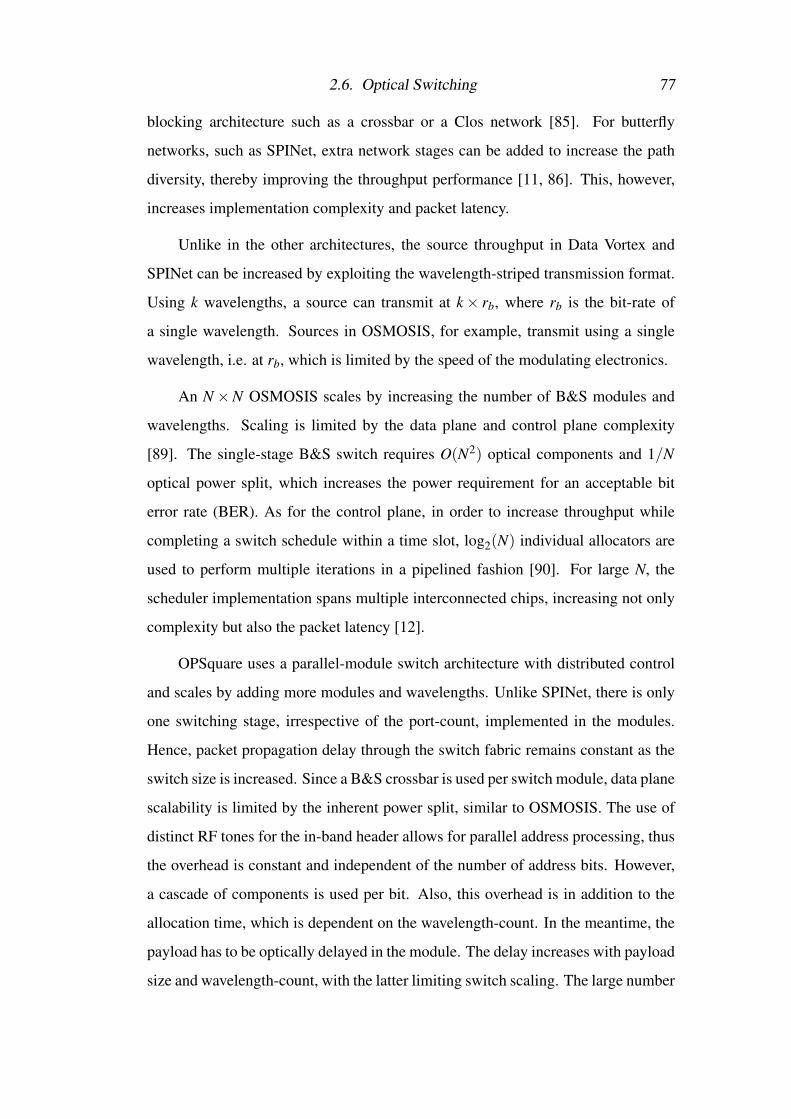
2.6. Optical Switching 77
blocking architecture such as a crossbar or a Clos network [85]. For butterfly
networks, such as SPINet, extra network stages can be added to increase the path
diversity, thereby improving the throughput performance [11, 86]. This, however,
increases implementation complexity and packet latency.
Unlike in the other architectures, the source throughput in Data Vortex and
SPINet can be increased by exploiting the wavelength-striped transmission format.
Using k wavelengths, a source can transmit at k× rb, where rb is the bit-rate of
a single wavelength. Sources in OSMOSIS, for example, transmit using a single
wavelength, i.e. at rb, which is limited by the speed of the modulating electronics.
An N×N OSMOSIS scales by increasing the number of B&S modules and
wavelengths. Scaling is limited by the data plane and control plane complexity
[89]. The single-stage B&S switch requires O(N2) optical components and 1/N
optical power split, which increases the power requirement for an acceptable bit
error rate (BER). As for the control plane, in order to increase throughput while
completing a switch schedule within a time slot, log2(N) individual allocators are
used to perform multiple iterations in a pipelined fashion [90]. For large N, the
scheduler implementation spans multiple interconnected chips, increasing not only
complexity but also the packet latency [12].
OPSquare uses a parallel-module switch architecture with distributed control
and scales by adding more modules and wavelengths. Unlike SPINet, there is only
one switching stage, irrespective of the port-count, implemented in the modules.
Hence, packet propagation delay through the switch fabric remains constant as the
switch size is increased. Since a B&S crossbar is used per switch module, data plane
scalability is limited by the inherent power split, similar to OSMOSIS. The use of
distinct RF tones for the in-band header allows for parallel address processing, thus
the overhead is constant and independent of the number of address bits. However,
a cascade of components is used per bit. Also, this overhead is in addition to the
allocation time, which is dependent on the wavelength-count. In the meantime, the
payload has to be optically delayed in the module. The delay increases with payload
size and wavelength-count, with the latter limiting switch scaling. The large number

2.6. Optical Switching 78
of components in the control path and the long optical delay waveguide in the data
path, impede the module’s photonic integration. In comparison, the wavelength-
striped packet format in SPINet and Data Vortex, allows for the modules to be
integrated; a much simpler address processing circuitry is required, adding a small
overhead, and payloads of arbitrary size can be delayed over short waveguides. The
LION switch does not need any address processing, due to the passive routing in
AWGRs, and OSMOSIS avoids it, as requests are electrical and the scheduler can
use them directly for allocation.
The LION switch architecture scales by using parallel AWGRs in the data
plane, in order to relax the constraints on the AWGR port count and wavelengths
required. The use of tunable lasers at the sources, increases the implementation
cost, compared to the other architectures that use fixed-wavelength transceivers.
However, the LION switch core is more energy efficient as it does not use any
active switching elements, such as SOA gates; packets are passively routed to their
destinations depending on their wavelength. Also, it suffers no power split as the
other architectures using B&S switching do. The switch is scheduled based on all-
optical arbitration, distributed to the switch output ports. This is implemented by
using an extra AWGR for every data plane AWGR, and placing an RSOA at every
output port, to perform local arbitration on a first-come, first-served basis. This has
the advantages of no O/E conversion at the switch, no address recovery overhead
and lower request-to-grant overhead, compared to the other architectures. However,
scheduling is completed upon arrival and processing of the grant back at the host
NIC, incurring a round-trip delay penalty, as already discussed. More importantly,
the optical arbitration scheme is not as effective as an electronic one would be, due
to limited processing capabilities in the optical domain. More specifically, unlike an
electronic arbiter, when there are multiple requests for the same output port at the
same time, the RSOA-based scheme grants none. Also, the first-come, first-served
priority has weak fairness compared to a round-robin arbiter.
Table 2.2 compares the architectures in terms of flow control, sorting them
according to scheduling delay, in decreasing order. The scheduling delay values

2.6. Optical Switching 79
Scheduling
Prototype Delay (ns) Size Method Request ACK
Data Vortex Module 5.0 2×2 Distributed Out-of-band No
SPINet Module 5.0 2×2 Distributed Out-of-band Yes
LION 9.0 32×32 Distributed In-band Yes
OPSquare Module 25.0 8×8 Distributed In-band Yes
OSMOSIS 51.2 64×64 Central Out-of-band Yes
Table 2.2: Flow Control Comparison for Different Switch Architectures
listed are calculated based on values published in the literature, in the respective
proof-of-concept discrete-component demonstrations.
Scheduling a 2×2 module in Data Vortex [83] and SPINet [87] is estimated at
5.0 ns. This includes the delays for address bit recovery and output port allocation.
It should be noted that this 5.0 ns scheduling delay will be incurred per architecture
stage, increasing the total scheduling delay. For an N×N SPINet, that is a minimum
of log2(N)× 5.0. The Data Vortex uses no ACK signalling and therefore has no
extra round-trip delay contribution to the total control delay, in contrast to SPINet.
In the OPSquare switch, a more complex address recovery circuit is required
due to the in-band header with encoded RF tones. A 15.0 ns address recovery
has been demonstrated [94]. This overhead is independent of the port-count. For an
8×8 crossbar, internal to a module, allocation added 10.0 ns. Unlike in Data Vortex
and SPINet, a packet experiences the scheduling delay only once, since OPSquare
has only one switching stage. The total control delay has an extra ACK transport
delay added.
In the LION switch, scheduling is optical and distributed to the AWGR output
ports, thus its delay is independent of port-count and estimated at 9 ns. This includes
a 5 ns round-trip delay to the RSOA, at the AWGR output, plus 4 ns for token
recovery at the network interface [99]. The latter assumes no more than two clock
cycles in a 500 MHz hardware implementation of the network interface. For the
total control delay, laser tuning time (≥ 8 ns) and ACK propagation delay are added.
OSMOSIS uses a time-slotted central scheduler for the entire 64× 64 B&S

2.6. Optical Switching 80
switch [12]. The time slot duration is 51.2 ns, determined by the fixed packet size
(256 Bytes) and transmission rate (40 Gb/s). The input requests are electrical and
thus can be used directly, without any O/E conversion or adding address recovery
overheads. Using the proposed FLPPR method [90], a grant can be issued in a time
slot. The speculative transmission scheme [92] allows packets to be forwarded to
the switch without waiting for a grant. An ACK has to be issued back to the source
to confirm packet receipt, increasing the total control latency.
Apart from OSMOSIS, the other reviewed architectures all encapsulate the
control functionality within the switch itself, similar to electronic packet switches.
In OSMOSIS, however, the control plane is physically separated from the data
plane, exposing its complexity to the overall network, due to the required control
wiring [11, 17]. Nevertheless, the two planes can be upgraded independently [89],
if necessary.

Chapter 3
System Concept
The proposed switch system concept, as part of a leaf-spine data centre network,
is presented in this chapter. This covers the control plane design, extending from
the servers to the switch, but also data plane aspects such as server transmission
format. The switch design is described in detail, including the choice of photonic
architecture, routing scheme and flow-control method. The aim is ultra-low packet
latency, which is key to realising optical packet-switched networking. In contrast to
an electronic switch, the design of an optical switch is transparent to bit rate. This
is exploited in the proposed system by using a broadband photonic architecture for
the switch and wavelength-division multiplexing transmission for the servers, to
substantially increase bit rate and reduce packet serialisation delay.
3.1 Switch ApplicationNanosecond-reconfigurable optical switches, at least up to a 64×64 size, have been
shown practical for photonic integration in SOA technology [23] or a combination
of MZI and SOA technologies [103, 80]. An optical switch of this size, can be used
to replace the currently electrical top-of-rack (ToR) switch, in the leaf-spine data
centre network.
The proposed data centre network concept is shown in Fig. 3.1. Optical ToR
switches interconnect servers and spine switches using WDM fibre links. Under
no path contention, packets from one server rack are switched to another, in two
hops. Every new packet is initially buffered in a first-in, first-out (FIFO) queue
3.2. Wavelength-striped Transmission 82
SPINE
LEAF
O/E E/On x m
NODES
O/E E/O
O/E E/O
O/E E/O
O/E E/O
O/E E/O
r x rNODES
m x nNODES
SERVERS
BUFFER
SCHEDULER
ToR
r-1 r-1m-1SOA
SOA
1 1 1SOA
SOA
0 0 0SOA
SOA
Figure 3.1: Proposed data centre network concept. Input-buffered optical top-of-rack(ToR) switch reduces minimum packet latency and avoids packet loss. A Closnetwork is a possible switch architecture. A dedicated scheduler reconfiguresthe switch in nanoseconds. Colour-coded in grey/black for electronic/electricalcomponents and in blue for optical components.
at the server network interface card (NIC). At the switch, packets may again be
buffered to resolve contention for a switch path. Buffering packets at the switch
a) reduces minimum packet latency and b) avoids packet loss. However, packets
failing allocation, due to contention, would require optical to electrical (O/E) and
electrical to optical (E/O) conversions, before traversing the switch, while the rest
of the packets cut-through the switch with no additional buffering. While O/E and
E/O conversions reduce the energy advantage of optical switching, they also allow
for regenerating optical signals. Hence, multiple such switches can be cascaded, to
scale the overall network size, as optical noise becomes irrelevant. The switch can
be implemented in a Clos architecture, to enhance scalability. A dedicated scheduler
is used to allocate switch paths and reconfigure the switch, in nanoseconds.
3.2 Wavelength-striped TransmissionA rack server connects to the ToR switch using an optical fibre link. Similar to the
Data Vortex and SPINet, the total bit-rate on the link is significantly increased by
using the WDM technology.
At the transmitter, every packet is divided into k segments and each segment is
serialised, at a fixed bit-rate, onto a specific wavelength. For example, a dedicated

3.3. Switch Architecture 83
D1D2Dk
Packet
D3
t
D1
D2
D3
Dk
Packet
t
(a) (b)
Figure 3.2: Packet transmission in (a) serial format and (b) wavelength-parallel format.
silicon photonic transceiver [104], integrated onto the server NIC, can be used per
wavelength. Enabled by WDM, the segments are then transmitted as one unit, in a
wavelength-parallel format, to the switch input port, as shown in Fig. 3.2.
This method, known as wavelength striping, has many benefits. It increases
the input port bandwidth to k times the wavelength channel bit rate. This, in
turn, increases switch capacity by a factor of k. Moreover, it reduces the packet
(de)serialisation delay, or head-to-tail delay, given by the ratio of packet size to the
input port bandwidth. Also, by dynamically reconfiguring how many wavelength
channels are bonded, based on the packet size, a low packet (de)serialisation delay
can be achieved, for variable-size packets.
3.3 Switch ArchitectureThe chosen switch architecture is important as it directly affects performance, such
as saturation throughput, its implementation complexity and scalability, but also the
practicality of the switch. That is, for example, if the switch can be integrated on a
single circuit or if it can be applied for packet or circuit switching. Also, based on
the architecture, the routing method and flow control are designed accordingly.
An optical packet switch needs to be reconfigurable on nanosecond timescales.
The broadband SOA technology, featuring sub-nanosecond switch transients, is
suitable for WDM photonic-integrated packet switching. For switch sizes up to

3.3. Switch Architecture 84
SOA
SOA
SOA
SOA
2 x 2
2 x 2
2 x 2
2 x 2
(a) (b)
Figure 3.3: Clos module architecture using parallel 2×2 SOA-based B&S switch elements.The fundamental (a) 2×2 switch element is used to build (b) a 4×4 module.An 8×8 module is built using the 4×4 module, and every twofold increase insize is implemented as such, recursively around the 2×2 base element.
N = 32, a single-stage B&S architecture can be used, which is logically equivalent
to a crossbar switch; strictly non-blocking and any input-output pair are directly
connected by a dedicated path, activated by turning “on” a single SOA gate. The
resulting space switch can therefore achieve a high throughput and benefit from
simplified routing as well as flow control. The inherent amplification in the “on”
state, compensates for losses due to splitting/combining and waveguide crossings,
and in the “off” state crosstalk is dramatically suppressed. However, ASE noise is
added to the switched packets. In a leaf-spine data centre network, a packet has
to traverse a cascade of up to three switches, which is not a significant number of
hops. More importantly, the proposed input-queued switch, regenerates contending
packets, eliminating any noise contribution per hop.
The N2 component requirement, as well as the high number of waveguide
crossings, prohibit large-scale implementations in a single B&S switch stage. To
scale the switch beyond N = 32, an (m,n,r) Clos network is proposed to be used as
the switch fabric. The modules in the Clos switch can be implemented, for example,
using parallel 2×2 SOA-based B&S switches [23], as illustrated in Fig. 3.3.
For an m= n= r =√
N, three-stage Clos switch, the module size is√
N×√
N.
Using B&S modules, N SOAs are required per module, keeping stage complexity
at a reasonable level. The total number of SOAs required for the Clos switch is
3N√
N. As shown in Fig. 3.4, the total count is smaller for N ≥ 16, compared to

3.4. Switch Routing 85
2 4 6 8 10
log2(N)
102
104
106
Tota
l S
OA
Count
Single-stage Switch - B&S
Clos Switch - B&S
Figure 3.4: Switch architecture comparison.
a single-stage B&S switch, such as the one in OSMOSIS. In a three-stage Clos
switch with B&S modules, only three SOAs are cascaded per data path, irrespective
of its size. Hence, ASE noise and saturation-induced distortion for high bit-rate
channels, remains at a fixed and low level as switch size increases. The Clos switch
scales by increasing the module size. Even though the module splitting/combining
losses increase with switch size, the SOA gain advantageously compensates for
those. This architecture therefore provides a good balance between the number of
switching stages and the loss at each stage, important for optical signal integrity. At
the same time, the relatively low stage complexity makes the switch practical for
photonic integration.
3.4 Switch RoutingRouting in the single-stage B&S switch is simple. There is one dedicated path,
directly connecting every input port to every output port. Once it allocates the
requested output port, the flow-control method executes routing by activating the
switching element (SOA) for that input-output pair. Due to the routing simplicity,
no additional control logic is required to make a routing decision, hence no control
overhead is incurred.
In an (m,n,r) Clos switch, there are m paths from an input port to an output
port. Routing logic is therefore required to choose a path, which can add a control

3.5. Flow Control 86
PACKETCONTROL
REQUESTCONTROL
λ1
λ2
λk
PACKET
t
REQUEST/FIFO FULL
RX
x N
SCHEDULER TO/F
RO
M S
PIN
E SW
ITCH
FRO
M S
ERV
ERTO
SER
VER
TX
N x NSWITCH
FIFO BUFFER
OPTICAL GATE
ELECTRICAL CONTROL
OPTICAL
VOQs
NIC
ToR SWITCH
Figure 3.5: Proposed system concept.
overhead depending on how the paths are assigned. For the proposed Clos switch,
with m = n = r, the traditional software looping algorithm [31], rearranges already
assigned paths, to add new paths, and iterates until any arising conflicts are resolved.
Although it enables rearrangeable non-blocking connectivity, the overhead can be
prohibitively long for packet switching. Other path assignment schemes, such as
random, rotating or static, may be used to reduce or even eliminate the routing
overhead, at the cost of a blocking probability.
3.5 Flow Control
The proposed system concept is shown in Fig. 3.5. The system is asynchronous and
operates in single clock cycle time slots. Global clock distribution, for the entire
network, is therefore avoided. At every server NIC, the packets are initially buffered
in a first-in, first-out (FIFO) queue. The Request Control reads the destination of
the head-of-line (HOL) packet and issues a request for a switch output port to the
scheduler. The request structure consists of a valid bit and an output port field of
log2(N) bits. Hence, a request can be efficiently transported to the scheduler over

3.5. Flow Control 87
SRC SWITCH DEST
SWITCH
CONFIG
ALLOC
REQ SYNC
GNT SYNC
GNT
PROCESS
REQ
GNT
SRC SWITCH DEST
SWITCH
CONFIG
ALLOC
REQ SYNC
REQ
SRC SWITCH DEST
SWITCH
CONFIG
ALLOC
REQ SYNC
REQ
ALLOC
SWITCH
CONFIG
(a) (b) (c)
time time time
Figure 3.6: Control delay comparison for two flow control methods: (a) non-speculative,(b) speculative - successful allocation and (c) speculative - failed allocation.
[log2(N)+1] low-speed parallel electrical wires, each carrying a single bit.
Once the request is sent, the Packet Control holds onto the HOL packet for a
configurable number of hardware clock cycles, before it forwards it speculatively
to the transmitter (TX). This delay, between request and packet transmission, is
fixed and determined by the scheduler delay, tscheduler, including allocation and the
switch reconfiguration. Thereby, the packet arrives at the switch as soon as it is
reconfigured.
Unlike bufferless switching, where a packet is stored at the source until an
ACK (or grant) is received, here every packet is forwarded to the TX speculatively,
without a scheduler grant. Thus, the source NIC implements a “send and forget”
scheme. As shown in Fig. 3.6, this reduces the control delay, by eliminating the
overheads for grant transport from the switch back to the server NIC and for grant
synchronisation and processing at the NIC. In case of failed speculation, the packet
is buffered at the corresponding switch input port, to avoid packet loss, and it is
forwarded to its destination in a subsequent switch reconfiguration round.
At the TX, the packet is serialised onto the WDM fibre link, in a wavelength-
3.5. Flow Control 88
striped format, and forwarded to the switch input port, as shown in Fig. 3.5. In
case of no packet contention, hence no failed speculation, the packet cuts through
the already reconfigured switch and is received at the destination with the minimum
end-to-end latency. Otherwise, the packet is stored at the switch input port.
At every switch input port, electronic buffering is implemented in a NIC, either
as a single FIFO queue or as N parallel FIFO queues, one for each output port. The
latter is known as virtual output queuing (VOQ). Compared to using a single queue,
the VOQ arrangement avoids the case where the HOL packet, while waiting to be
switched to its destination, blocks the preceding packets in the queue even though
they may be destined elsewhere. Thereby, the switch throughput is increased and
buffering delay is reduced, at the cost of increased scheduler wiring and allocation
complexity. Optical to electrical (O/E) and electrical to optical (E/O) conversions
are required when a packet is stored or released from a queue. Also, the packets
stored at the switch are wavelength-striped, which increases transceiver count. This,
however, is outweighed by the advantages of this transmission format, as outlined
in section 3.2.
The Request Control in the NIC, at every switch input, sends requests to the
scheduler in a parallel electrical format, just like at the sources. Switch NICs and
wiring to scheduler are not shown in Fig. 3.5, for diagram clarity. To implement
the VOQ buffering, N wires are required, compared to log2(N) for single-queue
buffering. Unlike speculative transmission at the sources, the Packet Control here
does not release the HOL packet from a queue, until a scheduler grant is received,
to avoid packet loss.
As shown in Fig. 3.5, for every switch input, a “FIFO full” signal is asserted,
when a queue is occupied beyond a threshold value, to notify the corresponding
source NIC to pause transmission (packets and requests). This provides control
backpressure and enables managing a small queue size at the switch inputs. Every
signal is either single-bit or an N-bit vector, if VOQ buffering is used. Overall,
this is the only control signalling from the switch back to the sources. The queue
threshold value depends on the propagation delay, tpropagation, between the switch

3.6. Review and Comparison to Related Work 89
and a source (round-trip) and the fixed delay before speculative transmission, tstx,
in the source buffer while scheduling completes. The threshold value is given by
the following equation and determines the minimum queue size required at a switch
input, to avoid packet loss up to 100% of input traffic load:
Threshold = tstx +2tpropagation (3.1)
The central scheduler is co-located with the optical switch, to keep the overhead for
control signal transport low. The scheduler receives two sets requests; one from the
sources, in response to new packets, and one from the switch, in response to packets
buffered at its inputs. The scheduler performs round-robin output-port allocation,
in parallel for the two request sets, and reconfigures the switch accordingly. This
includes the control signals for storing and releasing packets at the switch queues.
Priority is always given to switch requests, over new requests from the sources, for
strict in-order packet delivery and low packet latency. The scheduler delay is fixed,
dependent on the digital design. As shown in Fig. 3.6, it is the dominant control
path delay and, for packet switching, it has to be on packet timescales. However,
nanosecond scheduling becomes challenging as the switch size increases, due to
the allocation overhead. The next chapters discuss latency-optimised scheduling,
focusing on the allocation circuit design, to enable scalable packet switching.
In summary, the control plane latency is reduced by: (a) scheduler design,
(b) speculative transmission, (c) switch architecture and (d) switch routing. The
average end-to-end latency is further reduced by having: (a) wavelength-striped
packets and (b) virtual output queuing (VOQ) at the switch inputs. The focus of this
work is the scheduler design, optimised for clock speed and scalability.
3.6 Review and Comparison to Related WorkCompared to OPSquare, LION and OSMOSIS, in which a single wavelength is used
per source, the wavelength-parallel structure allows for a factor of k improvement
in transmission bandwidth, switch capacity and reduction in packet (de)serialisation
latency, for the same switch port count and packet size. If redundancy is employed,

3.6. Review and Comparison to Related Work 90
the number of parallel transceivers used can be increased dynamically to support
larger packets for the same or less serialisation latency. This is not an option for the
single-wavelength switch designs. Furthermore, wavelength-striped transmission
allows for a more cost-effective solution for E/O conversion. For example, a set
of k low-cost vertical-cavity, surface emitting lasers (VCSELs) or on-chip silicon
photonic transceivers can be used, to replace prohibitively expensive high-speed
serial transceivers [11]. These advantages come at the cost increased transceiver
count at the switch inputs, for storing wavelength-striped packets.
The Data Vortex and SPINet switch designs also increase throughput using
wavelength-striped transmission. In contrast to those designs, in the proposed
single-stage B&S architecture, being strictly non-blocking, the throughput saturates
at a higher fraction of capacity. The square law relationship, between component
count and port count, and the increasing waveguide crossings, however, limit size
to 32 ports, in a single-stage integrated B&S switch. The OSMOSIS switch scaled
to 64 ports using a discrete-component implementation with eight 8×64 broadcast
modules and sixty-four 8×1 select modules, in a parallel configuration. However,
high coupling losses, cost and footprint, associated with packaging the OSMOSIS
switch, make it impractical. The OPSquare switch has only two stages; one for
space switching and one for wavelength multiplexing. The switching stage also
uses a B&S configuration, which limits size to 64 ports. A viable LION switch size
is also 64 ports [105], limited by crosstalk and insertion loss, in a single AWGR
device. Larger sizes would also require more wavelengths to tune over at the
transceivers, increasing cost and complexity.
A Clos network with m = n = r, cascading smaller SOA-based B&S modules
in three-stages, is proposed to be used as the switch architecture for sizes greater
than 32 ports. Such architecture has been shown viable for scalable photonic-
integrated packet switching. Irrespective of switch size, the number of switch stages
remains fixed at three and so is the number of SOA cascades a packet traverses, if
single-stage B&S modules are used. This is important in data centre network as it
keeps the ASE noise and saturation-induced distortion per switch hop at a low level,

3.6. Review and Comparison to Related Work 91
important for low bit-error rate (BER). For comparison, a SPINet switch has at least
log2N stages, hence cascades more SOAs per data path, for N > 8. For example, a
64×64 SPINet requires cascading twice as many SOAs as the Clos switch, for the
same size.
As in the single-stage B&S switch, the OPSquare and LION switches require
no routing logic, since there is only one path from an input to an output. Also, the
LION switch benefits from passive routing, dependent on the packet wavelength.
However, there is a laser tuning overhead for passive routing, of the order of 10 ns,
compared to less than 1 ns reconfiguration for the SOA-based B&S architecture.
Routing a Clos switch is more challenging than a single-stage switch, because
there exist multiple paths through the switch, for every input-output pair. It requires
additional logic in the scheduler for route calculation, which increases complexity.
The delay of the traditional software looping algorithm, to converge to a routing
solution, would be prohibitively long for large packet switches. For high-speed
hardware implementation, a more practical approach is to assign predetermined
paths, similar to Data Vortex and SPINet, or choose a path randomly. However,
such routing schemes, trade off throughput for latency, as the Clos switch would
no longer be (rearrangeably) non-blocking. Nevertheless, the wavelength-striped
transmission can increase the switch throughput.
Transmitting parallel-electrical requests allows for (a) efficient transmission
and (b) simplified detection. Low-speed [log2(N)+1] wires can be used per source
to transmit requests. Since the scheduler is electronic, no O/E conversion is required
in the entire control plane. Compared to Data Vortex, SPINet, OPSquare and LION
switches, this simplifies detection by avoiding photodetectors in the control path.
In the proposed concept, having a single request bit per line, also simplifies request
synchronisation with the scheduler clock signal. Moreover, request transmission is
out-of-band which, compared to the OPSquare switch, avoids a cascade of multiple
components and associated overhead, for request/header recovery, per control path.
An input-buffered optical switch enables speculative packet transmission with
a “send-and-forget” source NIC. This eliminates the round-trip overhead for grant

3.7. Tools and Methodology 92
transport back to the source and also the overhead for grant processing, compared
to bufferless switch designs which store a copy of the packet at the source, until
a grant/ACK is received. In this way, the proposed switch design can achieve an
ultra-low minimum (no path contention) packet latency.
Although switch buffering based on fibre delay lines (FDLs) allows for all-
optical switching, the required waveguide length hinders the switch impractical for
photonic integration. In the proposed concept, silicon photonic transceivers and
fast dense electronic memory, is aligned with the industry goal to integrate CMOS
electronics with photonics, on a single chip, to share the packaging cost over a larger
system [106].
Electronic buffering at the switch, reduces the potential for energy and latency
merits of optical switching. Notwithstanding, it allows regenerating the optical
packets, per network hop, which makes the data centre network highly scalable,
as multiple network hops are supported.
As in OSMOSIS, in the proposed system concept, a dedicated centralised
scheduler is used per optical switch. This keeps the switching core all-optical
and separate from the control plane, which also allows for independent data plane
and control plane upgrade, if necessary. Centralised scheduling is sensible for the
single-stage B&S switch. In a multi-stage architecture, however, it is considered to
be adding a significant allocation overhead, because it handles requests from more
switch inputs, limiting scalability. The next thesis chapters are aimed at showing
otherwise; a centralised scheduler can be designed in a highly-parallel fashion, with
a small overhead on packet timescales, for large switch sizes. Additionally, central
scheduling can potentially increase allocation fairness, compared to a distributed
approach, due to its inherent global view of the allocation problem.
3.7 Tools and Methodology
A network emulator, with a packet level of detail, has been developed to model
the proposed system concept, in order to evaluate the switch performance for a
given traffic pattern. The main performance metrics used are the packet latency

3.7. Tools and Methodology 93
and switch throughput, to assess the choice of switch architecture, routing scheme
and flow control. The emulator and constituent hardware modules, are developed
in SystemVerilog, a hardware description language (HDL) for register-transfer level
(RTL) digital design and hardware implementation. An HDL emulator allows for
cycle-accurate measurements. For example, the end-to-end packet latency can be
reliably measured in hardware clock cycles, from the clock cycle a packet is injected
at a source to the clock cycle it is received at the destination. Another advantage
of using a SystemVerilog model is that key hardware modules, such as a source
NIC or the scheduler, can be directly synthesised as an ASIC or implemented on an
FPGA, to measure the minimum clock period. Hence, emulation latency results can
be translated from clock cycles to nanoseconds, for a highly-accurate measurement.
Scheduler synthesis and implementation is done using the Synopsys Design Vision
and Xilinx Vivado tools. The entire emulation is ran in Mentor Graphics ModelSim,
a simulation environment that allows network- and module-level verification. The
emulator setup is shown in Fig. 3.7, for an N×N switching system. It consists of N
packet sources, the network model and a packet sink.
A packet source is attached at every input port of the network. In the emulation,
the source generates packets of fixed size according to a given traffic pattern. As the
network model should be evaluated against a specific traffic pattern, a FIFO packet
queue is used in each source to isolate the applied traffic from the network. Given
an infinitely long queue, the network state cannot impact the traffic generation. For
instance, the case where a network input is unable to accept an injected packet, due
to a full buffer, is avoided. In the emulation, a queue with a depth of 4096 packets is
used. Packets are timestamped, before the source queue, so that the packet latency
includes the time spent in the queue. Next, the packets are forwarded to the network
and also to the packet sink, for counting.
At the packet sink, every packet arriving from the network is again counted
and timestamped. The packet latency is the time required for a packet to traverse
the network, from source to destination. It is calculated as the difference between
the two timestamps. The minimum packet latency is the main focus of the switch

3.7. Tools and Methodology 94
N x N Network
Data Plane
Control Plane
Switch Scheduler
Packet Sink
Packet SourceTraffic Gen
TXCount
TimeStamp
RXCount
Per
form
ance
Cal
cula
tio
n
PathAllocation
SwitchConfiguration
Packet Control
Backpressure Control
Control Propagation Delay
Request Control
Packet Buffering
Speculative Transmission
Packet Serialization Delay
TimeStamp
x N
Packet Propagation Delay
FPGA Board
Network Emulation Hardware Implementation
ASIC
Switch Scheduler
PathAllocation
SwitchReconfiguration
Switch Scheduler
PathAllocation
SwitchReconfiguration
Figure 3.7: Network emulation setup includes N packets sources, the N×N network undertest and the packet sink. The network module verifies control and data planefunctionality and adds delays to accurately model the system concept. Onceperformance is evaluated, the scheduler is either implemented on an FPGA orsynthesised as an ASIC.
design. Throughput describes the rate at which the network delivers packets to
their destinations. It is measured by counting the packets at each output port of the
network. A feature of interest is the saturation throughput and also how the network
behaves beyond saturation, as the input traffic load is increased.
The network model implements N server NICs, the allocator, and another set
of N NICs, one for each switch input. The packet sources are directly connected
to the server NICs, in a one-to-one mapping. Each server NIC has a FIFO queue,
as short as four packet entries, due to speculative packet transmission. The NICs
at the switch inputs, buffer packets either in a single FIFO queue or in N parallel
FIFO VOQs. Unless control backpressure is applied, the queue depth here varies
with input traffic load, and depends on buffering implementation (single queue or
parallel VOQs), switch architecture, routing and flow control. The switch buffering
requirement, for the different switch designs, is discussed in their respective thesis

3.7. Tools and Methodology 95
chapters. As shown in Fig. 3.7, in terms of functionality, the network model fully
implements the control plane, including NIC request and packet control for the
servers and switch inputs, scheduler allocation and switch reconfiguration, and also
backpressure control. The model includes data plane delays for packet speculative
transmission and buffering at the servers and switch. Extra delays are added for
control and packet propagation and packet (de)serialisation, to accurately capture
the latency characteristic of the proposed system concept.
The emulation is ran over four phases: reset, warm-up, measurement and cool-
off. A reset time of 100 clock cycles is used, over which the packet sources are
off and no packets are injected. During the warm-up period, the packet sources
are active, but the injected packets are neither counted nor are timestamped. The
warm-up period reduces the impact of systematic error on measurements. Without a
warm-up, packets injected early on in the emulation would have an advantage over
later packets, as they would see a more “empty” network, such as emptier buffers
and more idle resources. Hence, these packets would experience less contention
and lower latency. A warm-up period of 200 clock cycles is used to minimise the
influence of the initialisation. After warm-up, any packets injected are considered
as measurement packets and they are counted and timestamped at the source and
then once more at the sink. A measurement period of 10×103 clock cycles is used.
Finally, during the cool-off phase, the emulation is ran for as long as it takes for
all the measurement packets to be received at the sink. This could take up to an
additional 10×103 clock cycles, depending on the input traffic load.
The packet sources collectively generate the network workload. That is, the
traffic pattern applied at the network inputs, over time. In this network emulation,
the workload is synthetic, because it can capture the important aspects of a realistic
application-driven workload, while it is easier to design and control. A synthetic
workload has an injection process x, which is binary; a packet is injected when
x = 1, or not when x = 0. In the emulation, every packet source injects packets
randomly, using a dedicated Bernoulli process. In a clock cycle, the packet injection

3.7. Tools and Methodology 96
time (clock cycles)
1
xE(Tp) = 1 / rp
Figure 3.8: Behaviour of a Bernoulli process injecting packets at a rate rp over time. Theexpected injection period is E(Tp) = 1/rp.
probability is:
P(x) =
1− p, for x = 0
p, for x = 1
In this case, the injection rate, rp, is equal to p and it is the same for all packet
sources, in any given clock cycle. The behaviour of a source using a Bernoulli
injection process is illustrated in Fig. 3.8.
A universal traffic load parameter is input to the emulation to set the injection
rate for all sources. The emulation is ran through all four phases, for a given load in
the range 0% to 100%. At 100% input traffic load, every source generates packets
in every clock cycle. The following pseudo-code demonstrates how the Bernoulli
injection process is typically implemented:
Algorithm 2: Pseudo-code model of a Bernoulli injection processif rnd num( ) ≤ load then
inject packet( );end
The function rnd num( ) generates uniformly distributed random numbers in
the range 0 to 100. The SystemVerilog built-in function dist uniform( ) is used for
this purpose. As for the packet destinations, every packet source uses a dedicated
uniform distribution, to assign a random switch output port to every injected packet.
This is implemented by also using the dist uniform( ) function, but random numbers
here are in the range 0 to N−1, for an N×N switch.

3.7. Tools and Methodology 97
Parameter Value
T 3.2 ns
Switch Size (N) 4 - 256
tstx 1T , 2T , 3T
tserial 1T
tpropagation 3T
FIFO Depth ≥ (tstx +2tpropagation)
Traffic Load 5% - 100%
Table 3.1: Parameters for Network Emulation
The emulation parameters are listed in Table 3.1. The emulation clock period
(T ) is set to 3.2 ns, the same clock speed as a server NIC, assuming transmission at
10 Gb/s and a 32-bit parallel bus driving the serialiser. The size for the crossbar and
Clos switches ranges from 4 ports up to 256 ports. The scheduler delay (tscheduler)
depends on its design and the target is 1T or 2T for a crossbar switch, and 3T for
a Clos switch, irrespective of switch size. Thus, the delay before server packets are
speculatively forwarded to the local TX (tstx), is either 1T , 2T or 3T . The packet
serialisation delay (tserial) is 1T . The propagation delay (tpropagation), for packets and
control signals, is set at 3T to emulate the time-of-flight over 2 m connections to
and from the switch. This cabling length is considered sensible for a rack-scale
switching system. When control backpressure is used, from the switch buffers to
the server NICs, the buffer depth required at the switch inputs can be as short as
8 packets, for a crossbar switch. With backpressure, the FIFO depth is a function
of tstx and tpropagation. Otherwise, without backpressure, the minimum buffer size
requirement becomes a function of traffic load. For a set switch size, the emulation
is ran once for every input traffic load, in the range from 5% to 100%.
The packet latency is calculated by subtracting the two timestamps associated
with each packet. The result is an end-to-end measure, expressed in clock cycles.
The packet latency, in the proposed system, is given by the following equation:
tpacket = tctrl + tqueue + tpropagation + tserial (3.2)

3.7. Tools and Methodology 98
The term tqueue accounts for the queuing delay at a switch input, due to contention.
The contention probability increases with input traffic load. Therefore, the packet
latency is a function of the traffic load.
The term tctrl refers to the control plane delay, which is constant and given by:
tctrl = treq + tpropagation + tscheduler (3.3)
The control plane delay includes overheads for request generation, treq and the
scheduler delay, tscheduler. The treq delay is 2T , comprising 1T at the source and
1T at the server NIC. Also, the tpropagation term appears twice in the packet latency
calculation. In Equation 3.3 it refers to the request propagation, from the server
NIC to the scheduler, over an electrical wire. In Equation 3.2, it refers to the packet
propagation, from the switch to the destination, over optical fibre.
The scheduler delay is a function of T, depending on the scheduler design:
tscheduler = P×T (3.4)
The multiplication factor, P, is to account for the number of pipeline stages in the
scheduler design. Pipelining is a technique used to decrease the clock period in a
design. The work aims at designing a crossbar scheduler with up to two pipeline
stages (P = 2) and a Clos scheduler with up to three pipeline stages (P = 3). If no
pipelining is used, P = 1. More details on pipelining and how it can be applied on
the scheduler design, are discussed in the next chapters. Therefore, 1≤ tscheduler≤ 3,
as already mentioned.
The minimum tpacket occurs when a packet experiences no contention, as it
traverses the switch. That is, tqueue = 0 in Equation 3.2. Hence, the minimum
packet latency is constant, independent of the traffic load.
In the emulation, the latency sum for all measurement packets is divided by the
total packet count, to calculate the average packet latency. This is then plotted as a
function of input traffic load. At low loads, the average packet latency converges to
the minimum value, which is the focus of the proposed switch designs. As the load
3.7. Tools and Methodology 99
is increased, the contention probability between packets for a switch path increases,
leading to more packets being buffered at the switch, thus increasing queuing delay
(tqueue), and consequently the average packet latency.
The packet latency distribution, at specific traffic loads, is also interesting to
plot, to examine the length of the distribution tail. The “shorter” the distribution tail
the less variable and more deterministic the packet latency is, an important feature
for latency-sensitive applications. The average packet latency per input-output pair
can also be plotted, to investigate the allocation fairness at the flow level.
The switch average throughput, as a function of input traffic load, is another
important performance metric. For a given input traffic load, the average throughput
is calculated as the ratio of the total number of measurement packets to the total time
taken to receive them at the sink, in clock cycles. It is expressed as a fraction of
switch capacity, which is N packets/clock cycle for an N×N switch, to allow direct
comparison between different switch designs, including switch size, architecture,
routing and flow control. When average throughput is plotted against traffic load,
an important feature is the saturation throughput; the highest average throughput
value that matches the input traffic load. It is the point where demand meets supply.
Equally significant is the throughput performance beyond saturation; the switch is
said to be stable, if it continues to deliver packets at the peak throughput, after
saturation. This demonstrates a fair scheduler design.
Once all the emulation results are collected, the scheduler is synthesised as
an ASIC chip or implemented on an FPGA board. Results, such as minimum clock
period (Tscheduler) and resource utilisation, are collected. More importantly, by using
the minimum clock period results, the level of detail of the network emulation can
be further increased, from packet level to hardware level. MathWorks “MATLAB”
is used to express packet latency in absolute time, i.e. in nanoseconds.
Table 3.2, list the parameters used to express packet latency in nanoseconds.
The delay tsync represents the scheduler overhead for request synchronisation, due to
the asynchronous control plane. The synchroniser logic runs at the scheduler clock
period, Tscheduler. For a synchroniser implementation as a cascade of two registers,
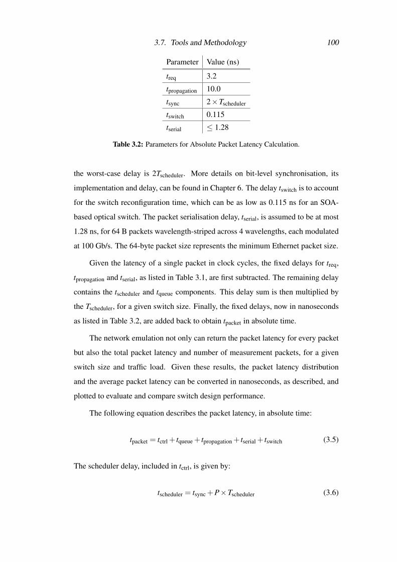
3.7. Tools and Methodology 100
Parameter Value (ns)
treq 3.2
tpropagation 10.0
tsync 2×Tscheduler
tswitch 0.115
tserial ≤ 1.28
Table 3.2: Parameters for Absolute Packet Latency Calculation.
the worst-case delay is 2Tscheduler. More details on bit-level synchronisation, its
implementation and delay, can be found in Chapter 6. The delay tswitch is to account
for the switch reconfiguration time, which can be as low as 0.115 ns for an SOA-
based optical switch. The packet serialisation delay, tserial, is assumed to be at most
1.28 ns, for 64 B packets wavelength-striped across 4 wavelengths, each modulated
at 100 Gb/s. The 64-byte packet size represents the minimum Ethernet packet size.
Given the latency of a single packet in clock cycles, the fixed delays for treq,
tpropagation and tserial, as listed in Table 3.1, are first subtracted. The remaining delay
contains the tscheduler and tqueue components. This delay sum is then multiplied by
the Tscheduler, for a given switch size. Finally, the fixed delays, now in nanoseconds
as listed in Table 3.2, are added back to obtain tpacket in absolute time.
The network emulation not only can return the packet latency for every packet
but also the total packet latency and number of measurement packets, for a given
switch size and traffic load. Given these results, the packet latency distribution
and the average packet latency can be converted in nanoseconds, as described, and
plotted to evaluate and compare switch design performance.
The following equation describes the packet latency, in absolute time:
tpacket = tctrl + tqueue + tpropagation + tserial + tswitch (3.5)
The scheduler delay, included in tctrl, is given by:
tscheduler = tsync +P×Tscheduler (3.6)

3.7. Tools and Methodology 101
A more accurate packet latency calculation allows for a more reliable comparison
between different switch designs, including architecture, routing and flow control.
The minimum scheduler delay, tscheduler, achievable on hardware, is important
for viable packet switching and it is the dominant component of minimum packet
latency, in a rack-scale system. The primary aim of the work is the design of a
nanosecond scheduler module, for large-size optical packet switching, in order to
achieve an ultra-low minimum packet latency. This particularly suited to latency-
sensitive applications and it is the subject of the subsequent thesis chapters.
Chapter 4
Crossbar Scheduler Design
The crossbar, as an architecture concept, has been widely deployed since the early
days of telephony networks. An N × N crossbar provides direct strictly non-
blocking connectivity between N ports, in a single stage. It does not require a
routing scheme and port-to-port paths are established by activating only one of N2
gating elements, laid out in a matrix configuration. A crossbar can also be used as
a switching module in other multi-stage architectures, such as a Clos network, to
increase network size. To this end, the focus of this chapter is the digital design of a
parallel scheduler for a crossbar switch architecture, optimised for clock speed, for
packet-switched networks. The chapter starts off with the baseline design, which
identified clock speed limitations, and then presents the proposed design which is
parallel in both dimensions, space and time, to significantly increase clock speed
and switch scalability. The design is compared to that in other crossbar schedulers
in the literature. Furthermore, the contributed designs discussed in this chapter have
been reviewed and published in [29].
4.1 Baseline Scheduler DesignThe scheduler is designed as a synchronous sequential circuit. It consists of parallel
combinational logic blocks and registers that hold the state of the scheduler. Every
F-bit register is a bank of F parallel flip-flops that share a common clock signal.
On the rising edge of the clock, the input bit at every flip-flop is transferred to the
output, and the output state (0 or 1), is held until the next clock edge. The scheduler

4.1. Baseline Scheduler Design 103
Gra
nt
MU
X
Arb
ite
r R
eq
ue
st
/
Arbiter
1
Arbiter
N-1
Allocator
Arbiter
0
Arbiter
1
Arbiter
N-1
Grant
Switch
Config.
Read-
Enable
Write-
Enable
/
/
/
/
N/
N
/
N
N
N
Arb
ite
r R
eq
ue
st
log2(N)+1
log2(N)+1
N
/N
NArbiter
0
1 2
R
/
RS
CCNFG
CRE
CWE
G
log2(N)+1
/
Figure 4.1: Scheduler design for an N ×N crossbar. There are two critical paths in thedesign, depending on N, shown in red.
design is synchronous because all registers receive the same clock signal. That is,
the state of the scheduler is synchronised to the clock.
Figure 4.1 shows a block diagram schematic of the scheduler design, for an
N ×N crossbar switch. The circuit has two banks of registers, one at the input
and one at the output. The input registers sample in the request matrix R, for new
packets at the source NICs, and the request matrix RS, for packets buffered at the
switch inputs. The output registers hold the current state for the grant matrix, G,
as well as the switch control signals for reconfiguration, CCNFG, and for storing
and releasing packets from the switch buffers, namely the write-enable, CWE and
read-enable, CRE, signals, respectively.
The Arbiter Request logic generates the arbiter requests. Every request in R
and RS consists of a port field, to indicate the output port requested, and also a
valid bit that marks the presence of a non-zero request, when asserted. For every
valid request, the Arbiter Request logic effectively performs a log2 N : N decoding
of the port field, so that an arbiter can process a request directly. The requests
are forwarded to the appropriate arbiter, depending on their port field. The entire

4.1. Baseline Scheduler Design 104
process is executed in parallel for R and RS, by using two copies of the Arbiter
Request logic, as shown in Fig. 4.1. The only difference between the two copies, is
that the logic for new packets ignores any requests from input ports for which RS
has valid requests. In this way, input port priority is given to packets buffered at
the switch. The purpose is to maintain strict in-order packet delivery, which also
reduces the average packet latency.
For every switch output port there is a dedicated N-bit arbiter. Therefore, each
arbiter handles at most N output port requests, from the input ports, in any given
clock cycle. The arbiters ensure that at most one request per output port is granted.
Every arbiter operates on the round-robin principle; the input port currently served
takes the least priority in the next round of arbitration, and the next input port in line
gets the highest priority. If that port does not have any request, priority decreases
sequentially from port to port. The entire arbiter set is referred to as the allocation
logic, or an allocator. As shown in Fig. 4.1, there are two parallel allocators, one for
R and one for RS. This approach allows to give priority to RS grants, without using
any feedback signalling that would slow down the scheduler, as described below.
The Grant Multiplexer (MUX) logic gives output port priority to packets
buffered at the switch, over new packets arriving from the servers. Since output port
allocation is executed in parallel and independently, it is possible that two arbiters,
in different allocators, grant the same output port to a new packet at the servers and
to a packet at the switch. Also, the two packets would be from different input ports,
since input port priority has already been given to packets buffered at the switch, in
the Arbiter Request logic for new packets. The Grant MUX logic ensures that only
the packet at the switch is granted the output port. The output vector of the Grant
MUX logic is used to create the next outputs of the scheduler circuit.
The priority vector, of any R arbiter, is updated only if the arbiter has issued
a grant, and that grant has not been filtered out by the Grant MUX. A feedback is
used from every RS arbiter to the R arbiter responsible for the same output port. In
Fig. 4.1, only the feedback for the first output port is shown, for diagram clarity.
The Grant logic generates the output vector G, which holds the grants issued

4.1. Baseline Scheduler Design 105
for new server packets. G is an N-bit vector in which every bit asserted indicates a
switch input port that is issued a grant. The Grant logic reads the output of the Grant
MUX, and asserts the appropriate bit for every grant that belongs to a new packet.
The significance of G is that every bit that is set high, corresponds to a packet that
will be switched with the minimum latency. More specifically, a server packet that
has won output port arbitration and does not contend with packets buffered at the
switch, neither for access to the switch input port nor for the destination output port.
The Write-Enable (WE) logic generates the output vector CWE to store new
packets from the servers, at the corresponding switch inputs. These are packets that
have either lost output port arbitration, due to contention with other server packets,
or competed for a switch input or output port, with packets already buffered at the
switch. The WE logic reads the Grant MUX output and generates the N-bit CWE.
Every bit asserted enables the buffer at a specific input port to store an incoming
packet, upon arrival at the switch.
The Read-Enable (RE) logic outputs the N-bit vector CRE, to release packets
buffered at the switch inputs. The RE logic checks the output of the Grant MUX, for
any grants that correspond to requests in RS, and asserts the appropriate bits in CRE.
For every switch input that a packet is to be released, a corresponding bit in CRE
is asserted. The packets are then switched to their destinations, with no additional
delay, as switch paths to the respective destinations are configured at the same time
as CRE is generated, as described next.
The Switch Configuration logic produces the output control signals in CCNFG,
to reconfigure the switch and setup paths through it, for the packets to traverse. The
logic reads the output vector of the Grant MUX and generates an output if any grant
is issued, irrespective of whether the grant is for a new packet or a packet buffered
at the switch. For every input port associated with a grant, the switch element
(SOA) to be activated, is addressed using log2(N) bits. Similar to the input request
matrices, an additional valid bit is used to indicate the presence of a valid switch
configuration. Therefore, in terms of size, the output CCNFG is an N× [log2(N)+1]
matrix.

4.1. Baseline Scheduler Design 106
0 10 20 30 40 50 60 70 80 90 100
Input Traffic Load (% Capacity)
0
10
20
30
40
50
60
70
80
90
100
Avera
ge T
hro
ughput (%
Capacity)
Ideal
4x4
8x8
16x16
32x32
Figure 4.2: Average switch throughput vs. input traffic load, under Bernoulli traffic.
The critical path in the design determines the minimum clock period of the
scheduler. As the switch increases in size, the critical path in the scheduler changes.
Both possible critical paths are marked in Fig. 4.1. For small switch sizes, the
critical path is from the RS register, through the one of the RS arbiters and Grant
MUX, to the priority register in one of the R arbiters. Hence, the priority-enable
feedback signalling from Grant MUX to the R arbiters, forms the critical path. For
larger switch sizes, the delay through the logic for the outputs increases, causing the
critical path to continue from the Grant MUX to the Grant logic. A more detailed
discussion on the critical path is presented in the hardware implementation section.
4.1.1 Network Emulation Results
One of the most important metrics to assess switch performance is throughput. The
average switch throughput is calculated as the ratio of all received packets to the
time taken to receive them. In Fig. 4.2, the average switch throughput is plotted as a
function of input traffic load, for different switch sizes. As previously explained, the
load is expressed as a percentage of capacity, in order to directly compare different
switch designs. In this case, it highlights the effect of switch size on the throughput
performance. The “ideal” throughput is also plotted in the graph as the baseline. It
represents the case in which a switch delivers packets at the same rate as they are
generated.

4.1. Baseline Scheduler Design 107
Throughput Saturation
Switch Size Traffic Load (%Capacity)
4×4 67.6
8×8 64.7
16×16 63.3
32×32 62.4
Table 4.1: Throughput Saturation Traffic Load vs. Switch Size.
As shown in Fig. 4.2, at low traffic levels, the function is linear with unity
gradient, for all switch sizes. That is, the switched traffic equals the offered traffic,
independent of switch size. As the load is increased, the switch eventually reaches
saturation, the highest throughput that matches input traffic load. The saturation
load is lower for larger switches, as shown in Table 4.1. However, the difference
is very small; the size penalty is approximately 5% between a 4-port switch and a
32-port switch. This demonstrates that the scheduler design can be scaled to control
larger switches with negligible degradation in switch average throughput.
The throughput results demonstrate that the switch is stable, irrespective of its
size. As the input traffic load increases beyond saturation, the average throughput
remains constant. A stable switch indicates that the underlying flow control method
is fair. In this case, the output-port allocation fairness is attributed to the round-robin
arbitration.
Buffering at the switch avoids packet loss while it enables speculative packet
transmission, at every server NIC, without ACK signalling. When no control back-
pressure is applied, the buffer size at the switch is a function of the input traffic load.
Figure 4.3 shows how the minimum buffer size varies as the load is increased, for
different switch sizes.
As expected, the buffer size increases with traffic load. For all switch sizes
examined, an 8-packet buffer is enough to support an input traffic load up to 25%
of port capacity. A buffer size of 16 packets enables lossless operation up to a
50% traffic load. Even for a packet size of 1500 B, which represents the Ethernet
maximum transmission unit (MTU), a 16-packet buffer translates to a small 24 KB
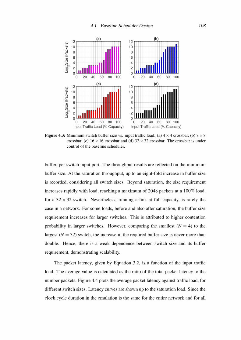
4.1. Baseline Scheduler Design 108
(a)
0 20 40 60 80 1000
2
4
6
8
10
12
Lo
g2S
ize
(P
acke
ts)
(b)
0 20 40 60 80 1000
2
4
6
8
10
12
(c)
0 20 40 60 80 100
Input Traffic Load (% Capacity)
0
2
4
6
8
10
12
Lo
g2S
ize
(P
acke
ts)
(d)
0 20 40 60 80 100
Input Traffic Load (% Capacity)
0
2
4
6
8
10
12
Figure 4.3: Minimum switch buffer size vs. input traffic load: (a) 4×4 crossbar, (b) 8×8crossbar, (c) 16× 16 crossbar and (d) 32× 32 crossbar. The crossbar is undercontrol of the baseline scheduler.
buffer, per switch input port. The throughput results are reflected on the minimum
buffer size. At the saturation throughput, up to an eight-fold increase in buffer size
is recorded, considering all switch sizes. Beyond saturation, the size requirement
increases rapidly with load, reaching a maximum of 2048 packets at a 100% load,
for a 32× 32 switch. Nevertheless, running a link at full capacity, is rarely the
case in a network. For some loads, before and also after saturation, the buffer size
requirement increases for larger switches. This is attributed to higher contention
probability in larger switches. However, comparing the smallest (N = 4) to the
largest (N = 32) switch, the increase in the required buffer size is never more than
double. Hence, there is a weak dependence between switch size and its buffer
requirement, demonstrating scalability.
The packet latency, given by Equation 3.2, is a function of the input traffic
load. The average value is calculated as the ratio of the total packet latency to the
number packets. Figure 4.4 plots the average packet latency against traffic load, for
different switch sizes. Latency curves are shown up to the saturation load. Since the
clock cycle duration in the emulation is the same for the entire network and for all

4.1. Baseline Scheduler Design 109
0 10 20 30 40 50 60 70
Input Traffic Load (% Capacity)
0
10
20
30
40
50
60
70
80
90
100
Avera
ge L
ate
ncy (
clo
ck c
ycle
s)
MIN4x48x816x1632x32
Figure 4.4: Average end-to-end packet latency vs. input traffic load, for different switchsizes. Network model assumes 3 clock cycles propagation delay to and fromthe switch, for both optical and electrical links. Packets are 1 clock cycle longand injected based on a Bernoulli process.
switch sizes, the minimum packet latency is fixed and it is plotted in the graph for
reference. In practice, the minimum clock cycle of the scheduler circuit increases
with switch size, which in turn results in a size-dependent minimum packet latency.
This is discussed in detail in the hardware implementation section below, where
also latency results, in nanoseconds, are reported up to a 100% traffic level.
At low loads, the average packet latency converges to the minimum value, as
shown in Fig. 4.4. As the traffic level is increased, the probability of contention is
higher, and therefore more packets are buffered at the switch. This is also evident
from the minimum buffer size results, which show an increase with traffic load, as
presented in Fig. 4.3. Hence, the packet queuing delay (tqueue) increases, which in
turn increases the average packet latency, for any switch size. All latency curves
exhibit a slow rate of increase with traffic load, with negligible difference between
them, up until a 55% load. As the saturation load is approached, the average packet
latency increases rapidly, and the increase is higher for larger switches, due to higher
contention. At 65% load, a difference of 45 clock cycles in average packet latency
is shown between the 4× 4 switch and the 32× 32 switch. Also, for these switch
sizes, there is a 5% difference in saturation load, which is in agreement with the
throughput results. The average packet latency, up to the saturation load, is less

4.1. Baseline Scheduler Design 110
Minimum LUT Count FF Count
Switch Size Clock Period (ns) (% Total) (% Total)
4×4 2.5 0.02 0.01
8×8 3.6 0.12 0.02
16×16 5.0 0.46 0.09
32×32 7.7 1.79 0.37
Table 4.2: Xilinx Virtex-7 XC7VX690T FPGA Timing and Utilisation Results.
than 100 clock cycles, for all switch sizes.
4.1.2 Hardware Implementation
Once the scheduler functionality has been verified and its performance tested, in
the network emulation, the next step is to implement the scheduler on a hardware
platform. The minimum clock period results can then be used to obtain a more
accurate measure of the packet latency, in nanoseconds, instead of clock cycles.
The scheduler is implemented on the Xilinx Virtex-7 XC7VX690T FPGA. The
lookup table (LUT) count and flip-flop (FF) count, for this device, are 433,200 and
866,400, respectively. A clock period constraint is specified and if the implemented
scheduler meets timing, the clock period constraint is decreased. This method is
repeated until the scheduler implementation fails timing, in order to determine the
minimum clock period. Table 4.2 lists the minimum clock period achievable, as
well as the percentage of LUTs and FFs used, for different switch sizes.
As shown in Table 4.2, the minimum clock period and resources utilisation are
increasing with switch size. For an N×N crossbar, an N-bit arbiter lies in the critical
path of the scheduler design. This causes the minimum clock period to increase, as
N is increased. Also, as expected, more scheduler LUTs and FFs are required for a
larger switch size. The number of LUTs and FFs used is approximately quadrupled,
when N is doubled. However, for the largest switch size, less than 2% of LUTs and
0.5% of FFs are used.
The number of FFs used is in agreement with the number of registers in the
scheduler design, including those in the arbiters that hold the priority state. This
4.1. Baseline Scheduler Design 111
verifies that the FPGA implementation tools have not removed any logic during
design optimisation, and therefore the scheduler design, as shown in Fig. 4.1, has
been fully implemented on the FPGA board.
The critical path in the design, which determines the scheduler minimum clock
period, is shown in Fig. 4.1. For small switch sizes, the critical path is formed due
to the feedback from the Grant MUX to the arbiters for new packet requests, used
to control when arbiter priorities are updated. As a result, the critical path starts
from the input register for the switch buffer requests, RS, through one of the arbiters
for RS, and terminates at the priority register of one of the arbiters for R. As the
switch size is increased, the signal delay through the logic for the outputs increases,
causing the critical path to continue from the Grant MUX to the output register for
the Grant logic.
Using the Tscheduler results, in Table 4.2, the minimum scheduling delay,
tscheduler, can be calculated using Equation 3.6, for every switch size. Since no
pipelining has been implemented in the scheduler design discussed so far, P = 1.
Therefore, tscheduler = 3Tscheduler, assuming worst-case tsync. Thus, the minimum
scheduling delay is 7.5 ns for the 4-port switch and 23.1 ns for the 32-port switch.
4.1.2.1 Packet Latency
As described in section 3.7, the packet latency for every switch size can be expressed
in nanoseconds, by using the minimum Tscheduler results, listed in Table 4.2, and the
fixed delays listed in Table 3.2.
The minimum end-to-end packet latency occurs when there is no contention
for a switch path. That is, in Equation 3.5, tqueue = 0. Substituting the minimum
Tscheduler results into the same equation, the minimum packet latency, for different
switch sizes, is as listed in Table 4.3.
Figure 4.5 shows the packet latency cumulative distribution function (CDF),
evaluated at 25%, 50% and 75% of traffic load, for 4 ≤ N ≤ 32. At a 25% load,
more than half of the packets are delivered with the minimum packet latency. Due
to higher contention probability, the fraction of minimum latency packets decreases,
as the switch size is increased. The fraction difference, however, is small; only 0.1

4.1. Baseline Scheduler Design 112
Minimum
Switch Size Packet Latency (ns)
4×4 32.1
8×8 35.4
16×16 39.6
32×32 47.7
Table 4.3: Minimum End-to-End Packet Latency vs. Switch Size.
difference between N = 4 and N = 32. Furthermore, the packet latency, including
the minimum value, is longer for larger switches. This is mainly due to the longer
scheduler clock period, which increases the total scheduler delay. The increasing
packet latency is exhibited in Fig. 4.5a as a right-shift, for every curve representing
a larger switch.
At a 50% traffic load, the fraction of packets with minimum latency is reduced,
for all switch sizes. For the 32×32 switch, only a tenth of the packets are delivered
with minimum latency. This is mostly due to the buffers at the switch being non-
empty. The scheduler is designed to give input port priority to packets buffered
at the switch, to maintain packet order and reduce average packet latency. More
specifically, the Grant MUX in the scheduler, will filter out any grant issued for a
new server packet, if the corresponding switch input has a non-empty buffer. By
filtering out new packet grants, less packets are delivered with minimum latency.
As the load is increased, it is more likely new packets face non-empty buffers at
the corresponding switch inputs. Apart from input port priority, the fraction of
minimum latency packets also decreases due to increased output-port contention,
either between servers or servers and switch buffers.
At a 75% load, the switch is in the saturation regime. New packets at the
servers, irrespective of switch size, see a more occupied switch; it is highly likely
that buffers at the switch inputs are not empty and contention for output ports is
high. As a result, very few packets are switched with minimum latency. Also,
compared to lower traffic loads, more packets are buffered at every switch input,
increasing the overall packet latency. In contrast to 25% and 50% traffic loads,

4.1. Baseline Scheduler Design 113
101
102
103
104
0
0.1
0.2
0.3
0.4
0.5
0.6
0.7
0.8
0.9
1
Cu
mu
lative
Pro
ba
bili
ty
(a)
4x4
8x8
16x16
32x32
101
102
103
104
0
0.1
0.2
0.3
0.4
0.5
0.6
0.7
0.8
0.9
1
Cu
mu
lative
Pro
ba
bili
ty
(b)
101
102
103
104
Packet Latency (ns)
0
0.1
0.2
0.3
0.4
0.5
0.6
0.7
0.8
0.9
1
Cu
mu
lative
Pro
ba
bili
ty
(c)
Figure 4.5: Cumulative distribution of the packet end-to-end latency at (a) 25%, (b) 50%and (c) 75% input traffic loads for different switch sizes. The Network modelassumes SOA-based crossbar with a 2 m link distance to every connectedsource and destination. Packets are 64 B, wavelength-striped at 4× 100 Gb/sand injected based on a Bernoulli process.

4.1. Baseline Scheduler Design 114
0 10 20 30 40 50 60 70 80 90 100
Input Traffic Load (% Capacity)
101
102
103
104
Avera
ge L
ate
ncy (
ns)
4x4
8x8
16x16
32x32
Figure 4.6: Packet end-to-end average latency vs. input traffic load, for different switchsizes. Network model assumes SOA-based crossbar with a 2 m link distance toevery connected source and destination. Packets are 64 B, wavelength-stripedat 4×100 Gb/s and injected based on a Bernoulli process.
the median packet latency is significantly higher, with a considerable difference
between different switch sizes.
The length of the “tail” of a CDF, is a measure of packet latency variance. Here,
the tail is defined as the latency difference between the 99th and 100th percentiles.
Figure 4.5 shows that the tail, for all switch sizes, at 25%, 50% and 75% traffic
loads, is very short. In fact, extending the tail definition to the 90th percentile, all
tails still remain very short. This indicates that the packet latency, even at traffic
levels as high as 75% of capacity, has a small variance.
The average packet latency in nanoseconds, for different switch sizes, is plotted
as a function of traffic load in Fig. 4.6. Based on the results, the 32×32 switch has
an average latency of approximately 100 ns at 60% load. For the same load, smaller
sizes achieve a lower average latency. Beyond the saturation traffic load, the average
latency increases rapidly for all switch sizes. For sub-microsecond operation, there
is a 5% decrease in maximum traffic load, as the switch doubles in size. At 100%
traffic load, the average latency is less than 10 µs for all switch sizes.

4.2. Pipeline Scheduler Design 115
Switch
Configuration
Allocation
Server
Request
Switch
Request
1
Server
Request
Switch
Request
2
Server
Request
Switch
Request
1
Server
Request
Switch
Request
2
Server
Request
Switch
Request
3
(a)
(b)
Legend
Time (clock cycles)
Figure 4.7: Scheduler design parallelism: (a) spatial and (b) temporal.
4.2 Pipeline Scheduler Design
In the previous section, the scheduler design presented is capable of processing new
server requests and requests from the switch, in parallel. This form of parallelism
is spatial, since two hardware copies of the Arbiter Request logic and Allocator are
used. A second form of parallelism is temporal, i.e. in time as opposed to space.
With temporal parallelism, also known as pipelining, multiple tasks are divided into
stages and they overlap in time.
Figure 4.7, illustrates the concepts of spatial and temporal parallelism, for the
scheduler design. As depicted in Fig. 4.7 (a), the scheduler discussed in the previous
section performs allocation for server and switch requests in parallel, followed by
the switch configuration. Allocation for new requests cannot start until the switch
configuration task is complete. With a pipeline design, however, a second round of
allocation can start, while the scheduler executes switch configuration for the first
round of allocation. As illustrated in Fig. 4.7 (b), the pipeline scheduler runs at

4.2. Pipeline Scheduler Design 116
Arb
ite
r R
eq
ue
st
Arbiter
1
Arbiter
N-1
Allocator
Arbiter
0
Arbiter
1
Arbiter
N-1
Grant
Switch
Config.
Read-
Enable
Write-
Enable
/
/
/
N/
N
N
N
N
Arb
ite
r R
eq
ue
st
log2(N)+1
log2(N)+1
N/
/N
Arbiter
0
Gra
nt
MU
X
R
/
RS
CCNFG
CRE
CWE
G
log2(N)+1
/N
/
1st
Stage:
Output-Port Allocation
2nd
Stage:
Switch Configuration
/
Figure 4.8: Scheduler design with 2-stage pipeline for an N×N crossbar. The critical pathin the design is shown in red.
twice the clock speed, enabling three rounds of switch configuration in the time the
original scheduler, without pipelining, produces only two switch configurations.
Pipelining is implemented by placing registers between combinational logic
blocks, to divide the circuit into P pipeline stages that can run at a lower clock
period. In the illustration in Fig. 4.7, the allocation and switch configuration tasks
are shown to take the same time to complete, which enabled creating a two-stage
pipeline with equal-length stages. This is an ideal case in which a circuit divided
into P pipeline stages, reduces clock period by a factor of P, for the same total
circuit delay. In practice, it is often not possible to divide a circuit into stages of
exactly the same delay, and also registers add delay. The minimum clock period is
determined by the pipeline stage where the critical path lies, i.e. the longest stage
in terms of time.
The proposed scheduler design, for a crossbar switch, uses both spatial and
temporal parallelism techniques, as illustrated in the block diagram in Fig. 4.8.
Output-port allocation for new server packets and packets buffered at the switch,

4.2. Pipeline Scheduler Design 117
is executed in a space-parallel fashion, as before. In the new design, pipelining
is implemented by registering the arbiter grants. This makes the scheduler a two-
stage pipeline; in the first stage the output-port allocation task is performed, and in
the second stage, the task of generating the new switch configuration is executed.
A second modification to the scheduler design is the absence of a priority-enable
feedback signalling to the arbiters for new packet requests. The implementation of
the non-pipelined scheduler revealed that a feedback in the design may form long-
delay paths or even the critical path, for small switch sizes. Removing the feedback
increases clock speed, at the expense of occasionally updating the priorities of the
R arbiters for non-winning grants.
The critical path in the pipelined scheduler design, is shown in Fig. 4.8. It
extends from the RS register, through one of the RS arbiters, to either the priority
register of that arbiter or the arbiter grant register.
4.2.1 Network Emulation Results
The switch performance, using the pipeline scheduler design, is evaluated in the
network emulation and compared to the one using the baseline design. The delay
before speculative packet transmission, tstx, is increased by a clock cycle, since the
scheduling now requires two clock cycles to complete, due to the pipeline design.
The switch average throughput, as a function of the input traffic level, is shown
in Fig. 4.9. Throughput curves for different switch sizes, as well as the “ideal”
throughput, are also plotted for comparison.
For all switch sizes, as the input traffic load is increased, the switch average
throughput equals the offered load, until it saturates at a certain load. Saturation load
decreases with switch size, as shown in Table 4.4. Compared to the baseline design,
the saturation load, for a given size, is approximately the same. Same as with the
baseline design, the pipeline design shows only a 5% decrease in saturation load,
as the switch is scaled from 4 ports to 32 ports, and the average throughput remains
constant beyond saturation. Therefore, the pipeline scheduler is fair and enables
scaling the switch size with a very small penalty in saturation throughput.
The minimum buffer size required at the switch inputs, as a function of traffic

4.2. Pipeline Scheduler Design 118
0 10 20 30 40 50 60 70 80 90 100
Input Traffic Load (% Capacity)
0
10
20
30
40
50
60
70
80
90
100
Avera
ge T
hro
ughput (%
Capacity)
Ideal4x48x816x1632x32
Figure 4.9: Average switch throughput vs. input traffic load, under Bernoulli traffic.
Throughput Saturation
Traffic Load (% Capacity)
Switch Size Baseline Pipeline
4×4 67.6 67.3
8×8 64.7 64.4
16×16 63.3 63.3
32×32 62.4 62.5
Table 4.4: Comparison of Throughput Saturation Traffic Load vs. Switch Size.
load and switch size, is shown in Fig. 4.10. The buffer size is shown increasing with
traffic level. Nevertheless, a small buffer size of 16 packets is enough for operation
up to 50% of capacity, for all switch sizes. Therefore, pipelining the scheduler
design has no effect on the switch buffer size, for loads as high as 50% of capacity.
As the load is increased beyond the saturation level, the minimum size requirement
increases at a higher rate, reaching a value of 2048 packets, for the larger switches.
Figure 4.11 shows how the average packet latency varies as a function of the
input traffic load, for 4≤ N ≤ 32. The minimum packet latency is also plotted and
it is one clock cycle longer compared to that in Fig. 4.4. This is because of the
pipelined scheduler design, which adds an extra clock cycle to tscheduler.
At low loads, all latency curves are shown converging to the minimum packet
latency. As the the load is increased, the curves exhibit a low rate of increase with

4.2. Pipeline Scheduler Design 119
(a)
0 20 40 60 80 1000
2
4
6
8
10
12
Lo
g2S
ize
(P
acke
ts)
(b)
0 20 40 60 80 1000
2
4
6
8
10
12
(c)
0 20 40 60 80 100
Input Traffic Load (% Capacity)
0
2
4
6
8
10
12
Lo
g2S
ize
(P
acke
ts)
(d)
0 20 40 60 80 100
Input Traffic Load (% Capacity)
0
2
4
6
8
10
12
Figure 4.10: Minimum switch buffer size vs. input traffic load: (a) 4×4 crossbar, (b) 8×8crossbar, (c) 16×16 crossbar and (d) 32×32 crossbar. The crossbar is undercontrol of the pipeline scheduler.
0 10 20 30 40 50 60 70
Input Traffic Load (% Capacity)
0
10
20
30
40
50
60
70
80
90
100
Avera
ge L
ate
ncy (
clo
ck c
ycle
s)
MIN4x48x816x1632x32
Figure 4.11: Average end-to-end packet latency vs. input traffic load, for different switchsizes. Network model assumes 3 clock cycles propagation delay to and fromthe switch, for both optical and electrical links. Packets are 1 clock cycle longand injected based on a Bernoulli process.

4.2. Pipeline Scheduler Design 120
Minimum LUT Count FF Count
Switch Size Clock Period (ns) (% Total) (% Total)
4×4 2.0 0.02 0.01
8×8 2.4 0.11 0.04
16×16 3.2 0.45 0.16
32×32 5.0 1.77 0.63
Table 4.5: Xilinx Virtex-7 XC7VX690T FPGA Timing and Utilisation Results.
a very small difference in value between them, up to 55% of traffic load. This
indicates that the average packet latency has a weak dependence on traffic load and
that it is fairly independent of switch size. As saturation is approached, the curves
rapidly slope upwards. The average packet latency remains below 100 clock cycles
up to the saturation load, for all switch sizes.
In summary, the network emulation results verify that the switch performs
equally well, in terms of throughput and packet latency, when the scheduler design
is pipelined. The minimum buffer size requirement, at the switch inputs, is higher
when pipelining is used. Nevertheless, for the largest switch (N = 32), a modest
size of 64 packets is required for zero packet loss up to the saturation throughput,
compared to a 32-packet buffer for the baseline scheduler design.
4.2.2 Hardware Implementation
The pipeline scheduler design has also been implemented on the Xilinx Virtex-7
XC7VX690T FPGA board, to allow for a direct comparison against the baseline
design. Table 4.5 lists the timing and resource utilisation results.
The timing results show that the scheduler minimum clock period increases
with switch size, but at a lower rate compared to the baseline design. Furthermore,
a significant decrease in minimum clock period is recorded, for all switch sizes.
For the 32×32 switch, the minimum clock period is reduced by 35%, from 7.7 ns
to 5.0 ns. This is because pipelining shortens the critical path in the design. As
shown in Fig. 4.8, the critical path is from the R or RS register, through one of the
corresponding arbiters, to either the Grant register or the arbiter priority register.

4.2. Pipeline Scheduler Design 121
Minimum
Switch Size Packet Latency (ns)
4×4 32.6
8×8 34.2
16×16 37.4
32×32 44.6
Table 4.6: Minimum End-to-End Packet Latency vs. Switch Size.
The FPGA resources utilisation also increases as the switch size is increased.
The rate of increase is the same with or without pipelining; resources used are
quadrupled when the switch is doubled in size. For a given switch size, the LUT
count for the pipeline design is slightly lower, since the logic associated with the
priority-enable feedback has been removed. However, the FF count is higher, since
more registers are used to pipeline the design. The FF count is as expected, hence
the entire scheduler circuit has been correctly implemented on the FPGA device.
Decreasing the minimum scheduler clock period, through pipelining, reduces
the total scheduling delay, as given by Equation 3.6. Since the scheduler design has
two pipeline stages, P = 2 and tscheduler = 4Tscheduler, assuming worst-case request
synchronisation. Substituting the Tscheduler results from Table 4.5, for 4 ≤ N ≤ 32,
the minimum scheduling delay is 8 ns ≤ tscheduler ≤ 20 ns, compared to 7.5 ns ≤
tscheduler ≤ 23.1 ns without pipelining.
4.2.2.1 Packet Latency
The packet latency is converted from clock cycles to nanoseconds. Table 4.6 lists
the minimum end-to-end packet latency, for different switch sizes, calculated using
Equation 3.5, with tqueue = 0. In the calculation, the fixed delays from Table 3.2 are
added to the scheduling delay, tscheduler, for a given switch size.
The minimum end-to-end packet latency, using the pipeline scheduler design,
is lower for all switch sizes. As expected, it increases with switch size, due to
the increasing scheduling delay, but at a lower rate compared to using the baseline
scheduler. For a 32×32 crossbar, the minimum packet latency is 44.6 ns.
The CDF for the packet latency, for different switch sizes and at different traffic

4.2. Pipeline Scheduler Design 122
loads, is shown in Fig. 4.12. At 25% traffic load, a large fraction of the packets
are received with the minimum latency. The fraction is higher for larger switches;
approximately 0.60 for N = 4 and 0.45 for N = 32. The difference in packet latency,
as the switch size is increased, is small. Also, for any switch size, all packets are
received with an end-to-end latency less than 100.0 ns.
At 50% traffic load, the fraction of minimum latency packets is significantly
reduced. It ranges from approximately 0.15 to 0.10, as N is increased from 4 ports
to 32 ports. The latency difference between switches of different size, is still small
at this traffic load. For N ≤ 16, the latency remains under 100.0 ns. For N = 32, all
packets are delivered with a latency less than approximately 145.0 ns.
At 75% traffic load, the fraction of minimum latency packets is very small.
Furthermore, the median latency is significantly increased, as the switch size is
increased. Also, the packet latency becomes more variable, for all switch sizes;
10% of the packets are received with a latency of approximately 100.0 ns and 90%
with a latency of approximately 1.0 µs or higher.
In Fig. 4.12, the CDF tail from the 99th, for all switch sizes and traffic loads, is
short. Hence, packet latency has a small variance, irrespective of switch size, even
at high traffic loads.
Pipelining the scheduler design reduces scheduling delay which in turn reduces
packet latency. Hence, all CDF curves in Fig. 4.12 appear as left-shifted compared
to the CDF curves for the baseline scheduler (Fig. 4.5). Even though the minimum
packet latency is shorter, with a pipeline scheduler, less packets are received with
the minimum latency. This penalty decreases with traffic load. Without a priority-
enable feedback in the design, an arbiter for new packets may update its priority for
a grant that is subsequently filtered out by the Grant MUX logic. This trades-off
round-robin effectiveness for clock speed, causing less packets to be switched with
the minimum latency. As the load is increased, less new packets are switched due
to the increasing packet queuing at the switch inputs, and the effect of no priority-
enable feedback is decreased.
Figure 4.13 plots the average packet latency against traffic load, for 4≤N≤ 32.

4.2. Pipeline Scheduler Design 123
101
102
103
104
0
0.1
0.2
0.3
0.4
0.5
0.6
0.7
0.8
0.9
1
Cu
mu
lative
Pro
ba
bili
ty
(a)
4x4
8x8
16x16
32x32
101
102
103
104
0
0.1
0.2
0.3
0.4
0.5
0.6
0.7
0.8
0.9
1
Cu
mu
lative
Pro
ba
bili
ty
(b)
101
102
103
104
Packet Latency (ns)
0
0.1
0.2
0.3
0.4
0.5
0.6
0.7
0.8
0.9
1
Cu
mu
lative
Pro
ba
bili
ty
(c)
Figure 4.12: Cumulative distribution of the packet end-to-end latency at (a) 25%, (b) 50%and (c) 75% input traffic loads, for different switch sizes. The network modelassumes SOA-based crossbar with a 2 m link distance to every connectedsource and destination. Packets are 64 B, wavelength-striped at 4×100 Gb/sand injected based on a Bernoulli process.

4.2. Pipeline Scheduler Design 124
0 10 20 30 40 50 60 70 80 90 100
Input Traffic Load (% Capacity)
101
102
103
104
Avera
ge L
ate
ncy (
ns)
4x4
8x8
16x16
32x32
Figure 4.13: Average end-to-end packet latency vs. input traffic load, for different switchsizes. The network model assumes SOA-based crossbar with a 2 m linkdistance to every connected source and destination. Packets are 64 B,wavelength-striped at 4×100 Gb/s and injected based on a Bernoulli process.
At low loads, all curves approach the minimum latency, as listed in Table 4.6. The
average latency shows a small increase with switch size and remains below 100.0 ns
up to the saturation loads, reported in Table 4.4. As the traffic load is increased
beyond the saturation level, the average latency increases at a high rate, for any
switch size. Doubling the switch size, reduces the highest load for sub-microsecond
latency by 5%. For operation at full input-port capacity, the average latency is well
below 10.0 µs, for all switch sizes. The average latency performance is better with
the pipeline scheduler design, due to the reduced scheduling delay component.
4.2.3 Crossbar Scheduler Comparison
The proposed scheduler is compared to other pipeline designs in the literature, for
a crossbar switch. More specifically, against the iterative parallel longest-queue-
first (ipLQF) scheduler [107] and the fast low-latency parallel pipelined arbitration
(FLPPR) scheduler [90] used in OSMOSIS. A more comprehensive flow-control
comparison, including scheduler design, is presented in section 5.2.5.1.
The OSMOSIS demonstration used a 64× 64 crossbar, built using discrete
components. Although a crossbar switch of this size is impractical for photonic
integration, the proposed scheduler is scaled to support this size, to allow for direct

4.2. Pipeline Scheduler Design 125
Switch Size
Scheduler 4×4 8×8 16×16 32×32 64×64
This Work 2.0 ns 2.4 ns 3.2 ns 5.0 ns 9.2 ns
ipLQF 6.4 ns 15.3 ns 33.3 ns - -
FLPPR - - - - 51.2 ns
Table 4.7: Minimum Clock Period for Different Scheduler Designs.
comparison between designs.
The proposed scheduler, for a 64× 64 crossbar, is implemented on the same
Xilinx Virtex-7 XC7VX690T FPGA device as for smaller sizes. The minimum
clock period achievable is 9.2 ns, indicating that the clock speed continues to scale
sub-linearly with the switch size.
The different schedulers are compared in terms of minimum clock period, as
published in the literature. Even though the ipLQF and FLPPR schedulers have
been implemented on different FPGA devices, the timing results should no vary
significantly from device to device, for a given design.
Table 4.7 lists the timing results, for different scheduler designs, as a function
of switch size. Compared to ipLQF, the proposed scheduler is significantly faster;
for a 16×16 crossbar, it can run at clock period 10 times shorter. Also, for a clock
period of 6.4 ns, the proposed scheduler can control a 32×32 crossbar, whereas the
ipLQF scheduler only a 4×4 crossbar. Against FLPPR, for a 64×64 crossbar, the
proposed design is more than 5.5 times faster.
The ipLQF and FLPPR schedulers are slower because they use more complex
allocation algorithms. Aiming at high switch throughput, both those schedulers
are designed to match crossbar outputs to inputs equipped with N VOQs, instead
of a single queue. Thus, the request size for allocation, per clock cycle, is N2,
compared to N for the proposed scheduler. The reduced design complexity allows
for a throughput-latency trade-off. Notwithstanding, a throughput higher than 60%
is achieved with the proposed scheduler, for the target 32×32 size.

4.3. Summary 126
4.3 Summary
This chapter focused on the design of parallel schedulers for crossbar switches,
applicable to packet-switched networks.
The baseline crossbar scheduler was first discussed, to present the clock speed
limitations in the design. It was found that the N-bit arbiter, used for the allocation
of a switch output port, lies in the critical path and limits clock period. Any feedback
signalling based on the arbiter results further increases critical path and therefore the
minimum clock period. The scheduler for a 32×32 crossbar was implemented on
the Xilinx Virtex-7 XC7VX690T FPGA and a minimum clock period of 7.7 ns was
achieved. This is also the minimum scheduling delay. For rack-scale switching of
64-byte wavelength-striped packets, at 4× 100 Gb/s, with an SOA-based crossbar
and asynchronous control plane, the minimum end-to-end packet latency for the 32-
port switch is 47.7 ns. In the network emulation, at this size, it was shown that the
crossbar throughput saturates at a load ≈ 60.0% of capacity with an average packet
latency of≈ 100 ns at this load, under control of the scheduler, for Bernoulli traffic.
A pipeline crossbar scheduler design was presented to increase clock speed
and scalability. The proposed design has two pipeline stages; one for fast round-
robin allocation of switch output ports, without any feedback signalling, and one
for generating the new switch configuration. Implementation on the same FPGA
as the baseline scheduler, for a 32-port crossbar, gave a minimum clock period of
5.0 ns. At this clock speed, the baseline scheduler can be used for a switch half the
size. However, due to the pipeline implementation, the minimum scheduling delay
is 2×5.0 = 10.0 ns, against 7.7 ns for the baseline scheduler. The delay benefit of
the pipeline implementation is evident in an asynchronous control plane scenario,
where up to two scheduler clock cycles are incurred for request bit synchronisation.
In that case, the minimum scheduling delay increases to 4× 5.0 = 20.0 ns and
3× 7.7 = 23.1 ns, for the pipeline and baseline designs, respectively. This results
in a minimum end-to-end packet latency of 44.6 ns, for the pipeline design. In
the network emulation, results showed that pipelining the scheduler reduces the
average packet latency, due to the shorter minimum clock period, without a penalty

4.3. Summary 127
in crossbar saturation throughput.
Compared to ipLQF and FLPPR, the pipeline scheduler design dramatically
increases clock speed, for the same switch size. More specifically, it is at least 10
times faster than ipLQF, for a 16-port crossbar, and 5.5 times faster than FLPPR, for
a 64-port crossbar. The trade-off is switch throughput. Both ipLQF and FLPPR use
complex scheduling algorithms to increasing the matching size for input-buffered
switches that use VOQs, aiming at 100% throughput. This significantly increases
their minimum clock period.
Despite the scheduler being scalable, the crossbar architecture is not, due to
the square law relationship between component-count and size. The next chapter is
dedicated to the scheduler design for scalable Clos-network optical switches.
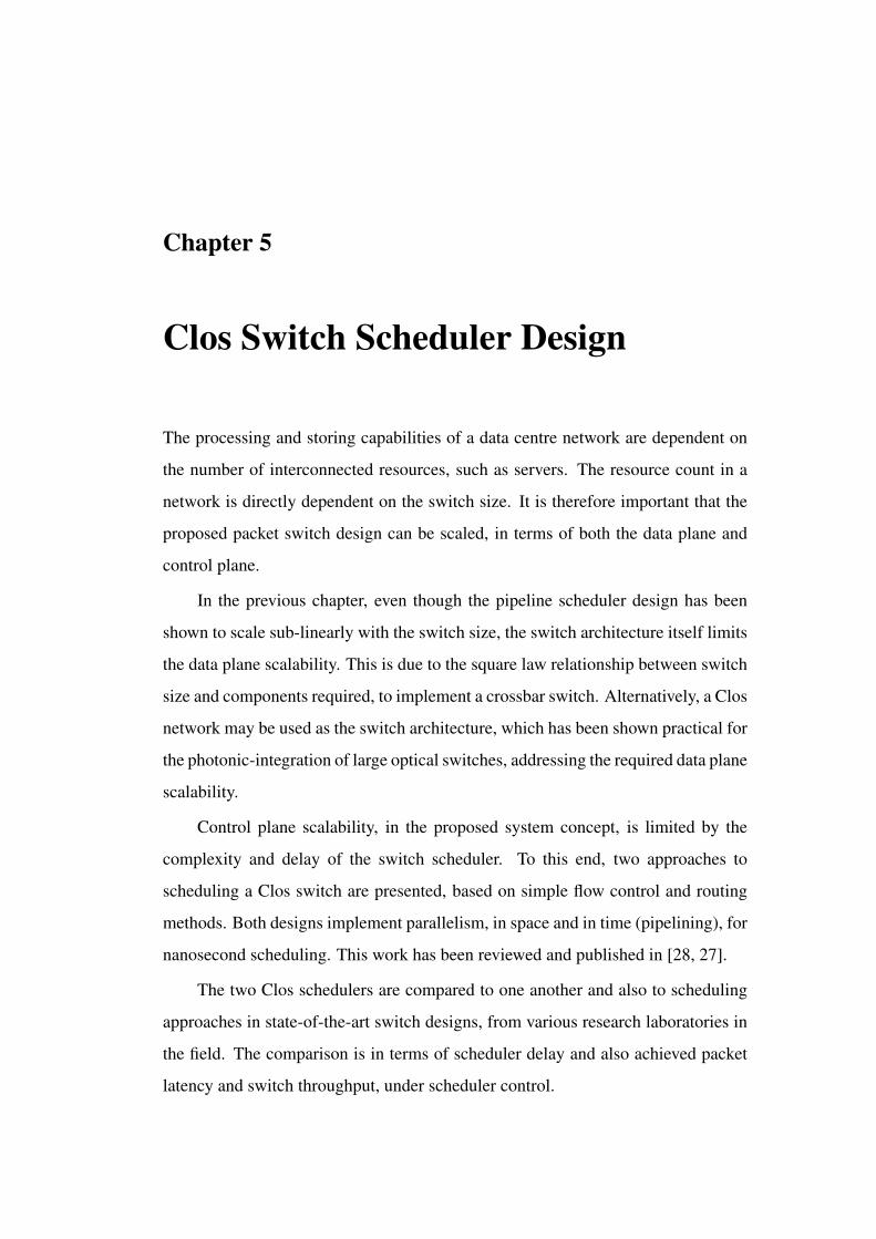
Chapter 5
Clos Switch Scheduler Design
The processing and storing capabilities of a data centre network are dependent on
the number of interconnected resources, such as servers. The resource count in a
network is directly dependent on the switch size. It is therefore important that the
proposed packet switch design can be scaled, in terms of both the data plane and
control plane.
In the previous chapter, even though the pipeline scheduler design has been
shown to scale sub-linearly with the switch size, the switch architecture itself limits
the data plane scalability. This is due to the square law relationship between switch
size and components required, to implement a crossbar switch. Alternatively, a Clos
network may be used as the switch architecture, which has been shown practical for
the photonic-integration of large optical switches, addressing the required data plane
scalability.
Control plane scalability, in the proposed system concept, is limited by the
complexity and delay of the switch scheduler. To this end, two approaches to
scheduling a Clos switch are presented, based on simple flow control and routing
methods. Both designs implement parallelism, in space and in time (pipelining), for
nanosecond scheduling. This work has been reviewed and published in [28, 27].
The two Clos schedulers are compared to one another and also to scheduling
approaches in state-of-the-art switch designs, from various research laboratories in
the field. The comparison is in terms of scheduler delay and also achieved packet
latency and switch throughput, under scheduler control.

5.1. Global Scheduler Design 129
5.1 Global Scheduler Design
Unlike a crossbar switch, a Clos switch requires routing. For a given routing
scheme, the only free decision is at the input module (IM), to choose one central
module (CM) out of m possible options. At the CM, the single path to the output
module (OM), where the requested output port resides, has to be chosen. Similarly,
at the OM, the requested output port must be chosen.
The looping algorithm, for non-blocking routing of Clos networks, iterates
the current routing matrix, rearranging entries where necessary, to choose a non-
conflicting CM. Such approach is impractical for scalable packet switching, due to
the long time required to converge to a solution.
Instead, a random path assignment is proposed, to allow choosing a path in
a single hardware clock cycle. The trade-off is switch saturation throughput; the
architecture becomes blocking, therefore the path allocation matching quality is
sub-optimal. This leads to less grants being issued per clock cycle, and thus a
decrease in saturation throughput. For a three-stage Clos switch, with random path
assignment, a request from any input port has to win output port arbitration three
times along the chosen path, once at every Clos module.
In the proposed design, the switch output ports, i.e. the OM output ports, are
globally allocated by considering all input port requests, just like for a crossbar
switch. For the IM and CM output ports, distributed allocation is performed by
taking into account requests from the local input ports only.
The block diagram in Fig. 5.1 illustrates the scheduler design for a Clos switch.
The design is divided into three pipeline stages: (a) global output-port allocation,
(b) distributed path allocation and (c) new switch configuration. The scheduling
delay is therefore fixed to three clock cycles. For an asynchronous control plane, an
extra clock cycle needs to be added for request synchronisation.
The first pipeline stage implements two parallel N×N output-port allocators;
one for R and one for RS. Each allocator is a set of N, N-bit round-robin arbiters,
one for each output port. In this way, allocation is performed globally, since each
allocator takes into account all N input ports of the switch, as opposed to those local

5.1. Global Scheduler Design 130
Arbiter
1
Arbiter
N-1
Allocator
N Arbiter
0/N
Arb
ite
r
Re
qu
est
/
Arb
ite
r
Re
qu
est
N x N
Allocator
/
Arb
ite
r
Re
qu
est
Arb
ite
r
Re
qu
est
Re
qu
est
MU
X
Gra
nt
MU
X
m x n
Allocator
Arb
ite
r
Re
qu
est
Re
qu
est
MU
X r x r
Allocator
Pa
th
Gra
nt
OM
Config.
/
COM
/
Grant /N
G
Write-
Enable/N
CWE
Read-
Enable/N
CRE
log2(m)+1
/
log2(N)+1
R
/
RS
Arb
ite
r
Re
qu
est
log2(N)+1
/N N
x r
x m
x r
x r
x m
x m
m
Port Grants
Path Grants
IM
Config.
CM
Config.
/
CCM
log2(r)+1
/
CIM
log2(n)+1
1st
Stage:
Output Port Allocation
2nd
Stage:
Path Allocation
3rd
Stage:
Switch Configuration
Figure 5.1: Scheduler design with 3-stage pipeline for an N×N Clos switch. The criticalpath in the design is shown in red.
to a Clos module. Global allocation is chosen for better fairness, compared to the
modular approach.
Multiple copies of the Arbiter Request logic generate the path requests, for
each IM and CM allocator. According to the proposed routing scheme, every IM
input port may request at most one random IM output port. The requested output
port on a CM depends on the packet destination. For the IMs, r copies are used
for the R matrix and r more for the RS matrix. The Request MUX logic filters out
any request in R that contends with an RS request, for an IM output port. Similarly,
2m copies of the Request Logic are used for the CMs, each followed by a Request
MUX to remove any conflicting R requests.
The second pipeline stage implements distributed path allocation, for routing
the Clos switch. For every one of r IMs, a dedicated m× n allocator reads the

5.1. Global Scheduler Design 131
corresponding (registered) request matrix, generated in the first pipeline stage, and
chooses at most one of n input ports for each local output port (or CM). Similarly,
for every one of m CMs, a dedicated r× r allocator chooses at most one of r IMs,
for every local output port (or OM). All IM and CM allocators operate in parallel.
The Path Grant logic reads the outputs of all IM and CM allocators and generates
an N×m matrix, to identify the path granted to each input port, if any.
Meanwhile, the Grant MUX logic processes the two (registered) output port
grant matrices, for R and RS, generated in the first stage. It filters out any R grant
that contends with an RS grant for an output port. The resulting N×N grant matrix
identifies the output port granted to each input port, if any. The port grant and path
grant matrices are registered into the third pipeline stage.
In the third pipeline stage, the corresponding port and path grant bits for every
input port are “ANDed” together, in the output logic for the Grant (G), Write- (CWE)
and Read-Enable (CRE) vectors and the Switch Configuration matrix (CCNFG). That
is, a request from an input port is only served if it is issued both an output port grant
and a path grant. If that request is from the R matrix, the corresponding G bit is
asserted. If it is an RS request, then the corresponding read-enable bit, in CRE, is
set high. For every valid request in R that fails output port or path allocation, the
appropriate write-enable bit, in CWE, is asserted. For every bit-pair in the port grant
and path grant matrices that is true, the appropriate SOA gate is addressed in CIM,
CCM and COM, to reconfigure the Clos modules.
The critical path in the design is marked on the block diagram in Fig. 5.1. It is
the same as that for the crossbar pipeline scheduler. It extends from either the R or
RS register, through one of the arbiters in the corresponding allocator, to the grant
register or the priority register, for that arbiter. Consequently, it is expected that
this Clos scheduler design can run at a clock speed as high as that for the proposed
crossbar scheduler.
5.1.1 Network Emulation Results
The scheduler design and routing scheme are evaluated for a 32× 32 Clos switch,
implemented in different architecture configurations. More specifically, the (4,4,8),

5.1. Global Scheduler Design 132
0 10 20 30 40 50 60 70 80 90 100
Input Traffic Load (% Capacity)
0
10
20
30
40
50
60
70
80
90
100
Ave
rag
e T
hro
ug
hp
ut
(% C
ap
acity) Ideal
(4,4,8) Clos
(8,4,8) Clos
(8,2,16) Clos
(16,2,16) Clos
Xbar
Figure 5.2: Average switch throughput vs. input traffic load, for a 32× 32 switch built indifferent architectures, under Bernoulli traffic.
(8,4,8), (8,2,16) and (16,2,16) Clos networks are examined. The (4,4,8) Clos
configuration is particularly interesting, as it is practical for photonic integration.
The remaining configurations enable to assess how effective the random routing
scheme is, as the ratio m/n is increased, which decreases the probability of path
contention.
Figure 5.2 shows the average switch throughput, plotted against the input traffic
load, for the different Clos configurations. The average throughput curve for a
32× 32 crossbar switch, with the pipeline scheduler design, is added to the graph
for comparison. As shown, the average throughput for the (4,4,8) Clos saturates
at the lowest traffic load and for the crossbar at the highest. As the m/n ratio is
increased, the saturation load increases, approaching that for the crossbar switch.
Table 5.1 lists the saturation load for the different 32×32 switch architectures. The
(8,4,8) Clos significantly increases saturation throughput, compared to the (4,4,8)
Clos. The (8,2,16) Clos and (16,2,16) Clos switches, not only are impractical for
photonic integration, but also offer a small gain in saturation throughput.
In the Clos scheduler, the switch output ports are allocated in the same way as
in the crossbar scheduler. The difference between the two designs is that the Clos
scheduler has an additional pipeline stage for routing. Therefore, the difference
in saturation throughput is interpreted as a measure of the routing scheme penalty.

5.1. Global Scheduler Design 133
Switch Throughput Saturation
Architecture Traffic Load (%Capacity)
(4,4,8) Clos 32.1
(8,4,8) Clos 47.5
(8,2,16) Clos 57.0
(16,2,16) Clos 60.2
Crossbar 62.5
Table 5.1: Throughput Saturation Traffic Load vs. 32×32 Switch Architecture.
Switch Minimum LUT Count FF Count
Architecture Clock Period (ns) (% Total) (% Total)
Crossbar 5.0 1.77 0.63
(4,4,8) Clos 5.4 3.20 0.85
(8,4,8) Clos 5.4 4.80 1.02
(8,2,16) Clos 6.1 6.57 1.55
(16,2,16) Clos 7.8 11.46 2.42
Table 5.2: Xilinx Virtex-7 XC7V690T FPGA Timing and Utilisation Results.
Based on the results, there is a 15% routing penalty in throughput performance,
between the (8,4,8) Clos switch and the crossbar switch.
5.1.2 Hardware Implementation
The scheduler is implemented on the Xilinx Virtex-7 XC7VX690T FPGA board,
for a 32× 32 switch size, built in different Clos network configurations. The aim
is to investigate the effect of switch architecture on the scheduler design timing and
resource utilisation. Table 5.2 lists the minimum clock period and LUT percentage
(out of 433200 available) and FF percentage (out of 866400 available). The results
for the pipeline 32×32 crossbar scheduler design are also included for comparison.
Compared to the crossbar scheduler, all Clos schedulers investigated use more
FPGA resources and therefore are more area-demanding. The scheduler for the
(4,4,8) Clos uses the least amount of LUTs and FFs on the FPGA device. Since
there is an allocator for every IM and CM, the LUT and FF utilisation increases
as m and r are increased, in the rest Clos configurations. The scheduler for the

5.1. Global Scheduler Design 134
Switch Minimum
Architecture Packet Latency (ns)
Crossbar 44.6
(4,4,8) Clos 51.6
(8,4,8) Clos 51.6
(8,2,16) Clos 55.1
(16,2,16) Clos 63.6
Table 5.3: Minimum Packet Latency vs. 32×32 Switch Architecture.
(8,4,8) Clos incurs the smallest increase, using less than 5% of available LUTs and
approximately 1% of the FFs. This represents only a 3.0% increase in LUTs and a
0.4% increase in FFs, compared to the crossbar scheduler.
The minimum scheduler clock period, for the (4,4,8) Clos and (8,4,8) Clos
switches, is the same and only 0.4 ns longer than that for the crossbar. This is
because the critical path in the three designs is the same; from one of the input
request registers, through one of the N-bit global allocation arbiters, to the grant or
priority register for that arbiter. The clock period is slightly longer for the two Clos
schedulers because of the path request logic in the first pipeline stage, which is not
present in the crossbar scheduler. For the (8,2,16) Clos and (16,2,16) Clos switch
schedulers, the minimum clock period is considerably longer. This is because the
critical path moves to the third pipeline stage, from either the port or path register
to the register for the output switch configuration logic.
5.1.2.1 Packet Latency
Using the scheduler timing results, the minimum packet latency for the different
32×32 Clos switches is calculated and listed in Table 5.3. The calculation assumes
2 m optical and electrical links, 64 B wavelength-striped packets at 4× 100 Gb/s
and an asynchronous control plane. For the (4,4,8) Clos and (8,4,8) Clos switches,
the minimum packet latency is 51.6 ns, against 44.6 ns for the crossbar switch. The
latency difference is due to the additional pipeline stage in the scheduler design, for
path allocation, and the slightly longer minimum clock period.
The average end-to-end packet latency, for the 32×32 Clos switches and also

5.2. Modular Scheduler Design 135
0 10 20 30 40 50 60 70 80 90 100
Input Traffic Load (% Capacity)
101
102
103
104
105
Ave
rag
e L
ate
ncy (
ns)
(4,4,8) Clos
(8,4,8) Clos
(8,2,16) Clos
(16,2,16) Clos
Xbar
Figure 5.3: Average end-to-end packet latency vs input traffic load, for 32× 32 switchesin different architecture and scheduler implementation on the Xilinx Virtex-7 XC7VX690T FPGA. The network model assumes SOA-based Clos switchwith a 2 m link distance to every connected source and destination. Packetsare 64 B, wavelength-striped at 4×100 Gb/s and injected based on a Bernoulliprocess.
for the crossbar switch, are shown in Fig. 5.3. The (4,4,8) Clos has the worst
latency performance and the crossbar switch the best. Sub-microsecond switching
for all Clos architectures, up to the saturation traffic load, is demonstrated. Apart
from the (4,4,8) Clos, the rest switch architectures allow for an average packet
latency less than 10 µs, when operated at full port capacity.
According to the network emulation and scheduler hardware implementation
results, the (8,4,8) Clos switch offers a good balance of practical architecture for
photonic-integration, low scheduler delay and packet latency, as well as moderate
switch throughput.
5.2 Modular Scheduler DesignThe (4,4,8) Clos switch, although suitable for photonic integration, it has a poor
throughput and latency performance, when random routing is applied. To improve
performance, doubling the number of CMs (m = 2n) was proposed, so that random
routing is more effective. Furthermore, an N ×N Clos switch scheduler, based
on global output-port allocation, can never run faster than an equivalent crossbar

5.2. Modular Scheduler Design 136
n x m
Input Modules
r x r
Central Modules
m x n
Output Modules
n
n
0
1
r-1
0
1
m-1
0
1
r-1
Figure 5.4: An (m,n,r) Clos network with strictly non-blocking modules. The proposedrouting scheme, for m = n = r Clos networks, assigns fixed paths to eliminaterouting overhead and avoid contention at the central modules, simplifying thescheduler design and reducing its delay.
scheduler. The clock speed is limited by the N-bit output-port arbitration, common
to both schedulers.
In this section, a scheduler design for Clos switches with m = n = r =√
N,
based entirely on distributed path allocation, is presented. The design requires
only√
N-bit arbitration, which significantly reduces scheduler delay and enables
a highly-scalable control plane. Additionally, a novel routing scheme is proposed to
limit scheduling delay to three clock cycles, i.e. to maintain a three-stage pipeline
design. To improve the switch saturation throughput and packet latency, VOQ
buffering at the switch inputs is considered. The trade-off is increased switch and
scheduler complexity.
5.2.1 Clos Routing
The proposed routing algorithm assigns dedicated paths, based on the source, i, and
destination, j, associated with a packet. The paths are assigned such that there can
be no output port contention at any CM. Figure 5.4 shows how the first path, to CM
0, is assigned at every IM. More specifically, at every IM, the first path/output port
leads to a different OM, thereby avoiding contention at CM 0. This is the case for

5.2. Modular Scheduler Design 137
the remaining paths as well. At any given IM, the path assignment to the OMs is a
circular shift by one position to the left, with respect to the previous IM, calculated
based on the following equation:
p(i, j) = (bi/nc+ b j/rc) mod m (5.1)
where 0≤ i, j ≤ N−1.
This routing algorithm benefits the scheduler design: (a) the route calculation
overhead is eliminated and (b) no path arbitration is required for the CMs. The latter
has the additional advantages of: (a) one less pipeline stage required, thus reducing
scheduling delay and (b) simplified scheduler implementation, since less hardware
resources are required.
As with random routing, the trade off is that the architecture is blocking, when
the paths requested are fixed. At every IM, at most one input port can be allocated
the route to a specific OM, even if different output ports on that OM are requested.
Hence, the switch throughput will saturate at a lower input traffic load, compared to
using the looping algorithm, for a given switch size.
5.2.2 Scheduler Hardware Modules
Since there can be no contention at the Clos CMs, distributed path allocation can
be implemented by having parallel output-port allocation modules, for the IMs and
OMs in the Clos switch. The allocation module for an IM, matches r OMs to n
local IM input ports (OM allocation). Similarly, the allocation module for an OM
matches n local output ports to r IMs (output-port allocation).
The block diagram in Fig. 5.5 illustrates the scheduler design for a Clos switch
with m = n = r. The design has three pipeline stages: (a) distributed OM allocation,
(b) distributed output-port allocation and (c) new switch configuration.
As shown in Fig. 5.6, the scheduler design can be visualised as having two
parallel path-allocation planes, one for processing new packet (server) requests and
the other one for processing VOQ packet (switch) requests. On each plane, there are
r allocation modules for the Clos IMs and r allocation modules for the Clos OMs,

5.2. Modular Scheduler Design 138
AR
BIT
ER
RE
Q.
AR
BIT
ER
RE
Q.
n x
r
iSL
IP
AL
LO
C.
r x n
AL
LO
C.
AR
BIT
ER
RE
Q.
n x
r
AL
LO
C.
AR
BIT
ER
RE
Q.
n x
r
AL
LO
C.
AR
BIT
ER
RE
Q.
r x n
AL
LO
C.
x r x r x r
x r x r
WR
ITE
EN
AB
LE
GR
AN
T
RE
AD
EN
AB
LE
OR
SW
ITC
H
CO
NF
IG.
2ND STAGE:
OUTPUT-PORT ALLOCATION
1ST STAGE:
OM ALLOCATION
3RD STAGE:
NEW SWITCH CONFIGURATION
RR
S
CC
NF
GC
RE
GC
WE
Figure 5.5: Scheduler design with 3-stage pipeline for an N ×N Clos switch, in whichm = n = r =
√N. The critical path in the design is in the 1st pipeline stage,
through the iSLIP allocator.
OM
Allocator
(1)
OM
Allocator
(r-1)
OP
Allocator
(0)
OP
Allocator
(1)
OP
Allocator
(r-1)
OM
Allocator
(0)
SW
ITC
H C
ON
FIG
UR
AT
ION
Input
Modules
Output
Modules
Figure 5.6: Clos switch scheduler design in a planar-modular visualisation. Planes operateindependently and in parallel to allocate paths based on output module (OM)and output port (OP) arbitration for the Clos input and output modules. Theswitch configuration module reconfigures the switch based on the allocationgrants from both planes.

5.2. Modular Scheduler Design 139
arranged in two different ranks and interconnected in a full mesh topology. The
module for switch configuration, processes the allocation results from both planes
to produce the configuration control signals for the Clos IMs and OMs. Also, every
allocation module, irrespective of rank and plane, makes decisions based on a group
of round-robin arbiters.
Based on the circuit visualisation in Fig. 5.6, the scheduler can be divided into
hardware modules, to optimise the design for clock speed. The hardware modules
are for: (a) OM allocation for the new packets plane, (b) OM allocation for the
switch VOQ packets plane, (c) output port (OP) allocation for both planes and (d)
new switch configuration. The module designs are presented next.
5.2.2.1 Output Module Allocation - New Packets
Figure 5.7 shows the OM allocation module design, used for every n× r IM in the
Clos switch. For every new server packet, that will be arriving on one of n IM input
ports, there is a switch output port request, based on the packet’s destination field.
Every one of these requests is held in matrix R and consists of a valid bit (v) and
an output-port field of log2(N) bits. A second matrix, RS, holds the higher-priority
requests from VOQ packets, on each IM input port. RS is used in this module only
for filtering purposes, as described below. Every request in RS is an N-bit vector and
the bit asserted, if any, addresses the requested output port. The circuit performs
allocation for any valid R request, that has not been filtered out, and generates the
matrices Gi and Gj to declare winning input ports and allocated OM output ports.
The Arbiter Request logic reads the RS requests to filter out any R requests
they contend with for IM input ports. This ensures input port priority to switch
VOQ packets, for strict in-order packet delivery. The logic then generates r n-bit
request vectors, one for each OM arbiter. Any bits asserted in a vector, indicate the
local IM input ports requesting a specific OM. Every arbiter then grants at most one
of n requests, based on round-robin priority.
The Grant logic generates the circuit’s output matrices, Gi and Gj, based on the
arbiter grants. Each matrix has at most r grants, one for every OM. Every grant in
Gi is a structure with an input-port field of log2(N) bits and a valid bit, to indicate

5.2. Modular Scheduler Design 140
/Arbiter
0
Arbiter
1
Arbiter
r-1
/n
Input Port
Selection
/n
/n
/n
/n
/n
x r
x r
log2(N)+1
/n
Gj
Gi
log2(N)+1
/
x n
N
/
x nRS
R
A B
Arb
iter
Re
quest
Gra
nt
Figure 5.7: Output module allocator design for new packets. The critical path in the designis shown in red. Tags A and B are for cross-reference with Fig. 5.8.
0 0 1 0
0 0 0 0
0 0 1 0
0 1 0 0
Output
Module
0 0 1 0
0 0 0 0
0 0 0 0
0 1 0 0
Output
Module
Gj
Ou
tput
Mo
du
le 0 0 0 0 0
1 0 1 0 0
2 0 0 1 0
3 0 0 0 0
Output
Port
Gi
Ou
tput
Mo
du
le 0 0 0
1 7 1
2 4 1
3 0 0
Input
Port
v
RS
Inp
utP
ort
4 0 0 0 0 0 0 0 0 0 0 0 0 0 0 0 0
5 0 0 0 0 1 0 0 1 0 0 0 0 0 0 0 1
6 0 1 0 0 0 0 0 0 0 0 0 0 0 0 0 0
7 0 0 0 0 1 0 0 0 1 0 0 0 0 0 0 0
R
Inpu
tP
ort
4 10 1
5 4 1
6 8 1
7 5 1
Output
Port
v
A B
12840Output Port
01
23
OM0
45
67
OM1
OM2 10
11
98
Figure 5.8: Example request processing for new packets by the output module allocator,for the 2nd input module in a (4,4,4) Clos switch. Binary matrices are taggedfor cross-reference with the digital design in Fig. 5.7.
the switch input port granted that OM. Every Gj grant is a one-hot n-bit vector and
the bit asserted, if any, indicates the granted output port on that OM.
Every valid grant pair, one from Gi and one from Gj, forms a request that is
forwarded to the appropriate output port (OP) allocation module, on the same plane.
The OP allocation module design is discussed in section 5.2.2.3.
Figure 5.8 illustrates an example of the circuit functionality, in a (4,4,4) Clos
scheduler. The input request matrices for new packets and switch VOQ packets,
R and RS, are for the second input module (IM 1), whose input ports are in the
range 4 to 7. Tags A and B are used for cross-reference with the design in Fig. 5.7.

5.2. Modular Scheduler Design 141
The Arbiter Request logic generates a binary matrix containing the arbiter requests
(Tag A), ignoring input port 5’s request as it contends with a VOQ request for the
same input and output ports. Next, every arbiter resolves any OM contention by
operating across a matrix column, selecting only one input port for that OM (Tag
A). The Grant logic generates the output matrices Gi and G j, based on the arbiter
grants (Tag B).
5.2.2.2 Output Module Allocation - Switch VOQ Packets
As shown in Fig. 5.9, the OM allocation module for IM VOQ packets requires a
more a complex design, compared to that for new server packets. This is because
there could be up to N switch output port requests at the same time, per IM input,
due to the VOQ buffering. The module allocates OMs to IM input ports, for a
chosen output port. In the scheduler plane for VOQ requests (Fig. 5.6), an instance
of the module is used for every n× r IM in the Clos switch. The circuit is a two-
stage pipeline and performs allocation based on the corresponding RS, to generate
the Gi and Gj matrices.
In the first pipeline stage, the Arbiter Request logic generates n, r-bit vectors,
one for every input port, and any bits asserted indicate the requested OMs. An
input-first n× r separable allocator is then implemented. Every first-rank arbiter
chooses at most one of r OM requests, for every IM input. Next, every second-rank
arbiter chooses at most one of n IM inputs, for every OM. The iSLIP method is used
to stagger the arbiter priorities. Although multiple iterations can be performed, to
further increase the number of grants and therefore the switch throughput, only a
single pass (1-SLIP) is executed to minimise the total scheduler delay. In iSLIP,
the priority of a first-rank arbiter is updated only if its grant output has also won
arbitration in the second arbiter rank. This creates a feedback which forms the
critical path in the design. In Fig. 5.9, only the feedback between the first two
arbiters is shown, for diagram clarity.
An additional allocation round is required for the winning requests. Due to
VOQ buffering, an IM input port matched with an OM, could be requesting up to n
of its output ports. Thus, an r×n allocator is used to choose one, since for unicast

5.2. Modular Scheduler Design 142
/
RS
Arbiter
1
Arbiter
n-1
Arbiter
1
Arbiter
r-1
Arbiter
0
Arb
iter
Re
quest
Arbiter
1
Arbiter
r-1
/r
OM
Selection
Input Port
Selection
/n
/n
/n
Output Port
Selection
Gra
nt
/n
/n
/n
/n
/n
/n
/n
/n
/r
/r
/
x r
x r
log2(N)+1
/n
Gj
Gi
/N
/N
/N
Arb
iter
Re
quest
N
/N
/N
x n
Arbiter
0
Arbiter
0
A B C D E
Figure 5.9: Output module allocator design for switch VOQ packets. The critical path inthe design is shown in red. Tags A-E are for cross-reference with Fig. 5.10.
RS
Input P
ort
4 0 0 0 0 0 0 0 0 0 0 0 0 0 0 0 0
5 0 0 0 0 1 0 0 1 0 0 0 0 0 0 0 1
6 0 1 0 0 0 0 0 0 0 0 0 0 0 0 0 0
7 0 0 0 0 1 0 0 0 1 0 0 0 0 0 0 0
Input
Port
4 0 0 0 0
5 0 1 0 1
6 1 0 0 0
7 0 1 1 0
Output
Module
Outp
ut M
odule 0 0 1 0 0
1 1 0 0 1
2 0 0 0 0
3 0 0 0 0
Output
Port
Gi
Outp
ut
Module 0 6 1
1 5 1
2 0 0
3 0 0
Input
Port
v
Gj
0 1 0 0
1 0 0 0
0 0 0 0
0 0 0 0
Output
Port
0 0 0 0
0 1 0 0
1 0 0 0
0 0 0 0
Output
Module
0 0 0 0
0 1 0 0
1 0 0 0
0 1 0 0
Output
Module
12840Output Port
EDCBA
01
23
OM0
45
67
OM1
0 1 0 0
1 0 0 0
0 0 0 0
0 0 0 0
Output
Port
Figure 5.10: Example request processing for switch VOQ packets by the output moduleallocator, for the 2nd input module in a (4,4,4) Clos switch. Binary matricesare tagged for cross-reference with the digital design in Fig. 5.9.
traffic only one output port request is permitted per input port. This additional
allocator is implemented in the second pipeline stage. The two allocators effectively
operate in a master-slave configuration, divided over two pipeline stages, with the
iSLIP allocator acting as the master.
As in the OM allocation module for new server packets, the Grant logic here
generates two matrices, Gi and Gj, to hold the input- and output-port grants, for
every matched OM. Every Gi-Gj grant pair, for an OM, is forwarded to the dedicated
OP allocation module, in the scheduler plane for IM VOQ packets (Fig. 5.6).
Figure 5.10 continues on the previous example (Fig. 5.8), to describe how an

5.2. Modular Scheduler Design 143
OM allocation module for IM VOQ packets, in the same (4,4,4) Clos scheduler,
functions. The hardware module is also for the second IM (IM 1), but operates in the
other scheduler plane (Fig. 5.6). The same request matrix, RS, is input to both OM
allocation modules in the two planes, at the same time. As shown in Fig. 5.10, the
Arbiter Request logic generates the binary request matrix for the first-rank arbiters.
For every input port, with a non-zero output port request in RS, the logic generates a
request for the corresponding OM (Tag A). Every first-rank arbiter operates across a
matrix row, to choose one requested OM from every input port (Tag A). The arbiter
grants (Tag B) are forwarded to the appropriate second-rank arbiters. Every second-
rank arbiter operates across a matrix column, to choose one input port for every
OM (Tag B). The Gi matrix is created directly, based on the second-rank arbitration
grants (Tag C). An additional arbitration round is executed, before G j is created.
In the second pipeline stage, the Arbiter Request logic generates the binary request
matrix for the arbiters. For every granted OM, for which there is a non-zero output
port request in RS, the logic asserts the corresponding request bit (Tag D). Next,
every arbiter chooses at most one output port for a specific OM (Tag D). Finally, the
arbiter grant matrix (Tag E) is used directly as the output G j matrix. In the example,
for input port 5, the first port on OM 1 (output port 4) is chosen.
5.2.2.3 Output Port Allocation
The output port allocation module design, for an r× n OM, is shown in Fig. 5.11.
The same module design is used in both scheduler planes (Fig. 5.6). The circuit
receives one Gi grant and one Gj grant, from every OM allocation module on the
same plane. Every grant pair forms a local output port request, from a specific IM.
The module matches local output ports to IMs and generates the final grant matrix,
G, to indicate the winning input ports. It also outputs two vectors; SOM, to indicate
winning IMs, and SOP, to indicate allocated ports.
The input port (IP) Map logic, reads the port field (0 to N− 1) of every input
Gi grant, and maps it to one of n input ports on the associated IM. This enables
the Grant logic to group output grants per IM. The IP Map logic generates an n-bit
vector, for every IM, and the bit asserted indicates the IM input port.

5.2. Modular Scheduler Design 144
//
Arbiter
0
Arbiter
1
Arbiter
n-1
IM
Selection
/log2(N)+1
OM
Sta
te
n
/n
/r/
r/r
/r
/r
/r
/r
OP
Sta
te
/r
/n
x N
SOM
SOP
Gx rx r
log2(N)+1
/
/
/
x r
n
n
n
Arb
iter
Re
quest
IP
Map
Gi
Gj
A
B C
Gra
nt
Figure 5.11: Output port allocator design. The same design is used for new packets andfor switch VOQ packets. The critical path in the design is shown in red. TagsA-C are for cross-reference with Fig. 5.12.
Gi
OM
Input
Port
12 1 3
Input
Module
2 1 0
5 1 1
10 1 2
Switch
In. Port
v
Gj
OM
Input P
ort
1 0 0 0 3
Input M
odule
0 1 0 0 0
1 0 0 0 1
0 0 1 0 2
4 5 6 7
Output
Port
Input M
odule 0 0 0 1 0
1 0 1 0 0
2 0 0 1 0
3 1 0 0 0
OM
Input Port
Input M
odule 0 0 1 0 0
1 1 0 0 0
2 0 0 1 0
3 1 0 0 0
4 5 6 7
Output
Port
SOM
Input M
odule 0 1
1 1
2 1
3 0
SOP
Outp
ut
Port 4 1
5 1
6 1
7 0
A
B
0 1 0 0
1 0 0 0
0 0 1 0
0 0 0 0
4 5 6 7
Output
Port
C
G
0 0 1 0 0 1 0 0 0 0 1 0 0 0 0 0 v
0 0 5 0 0 4 0 0 0 0 6 0 0 0 0 0
Outp
ut
Port
12840
Switch Input Port
Figure 5.12: Example request processing by the output port allocator for the 2nd outputmodule, in a (4,4,4) Clos switch. Binary matrices are tagged for cross-reference with the digital design in Fig. 5.11.

5.2. Modular Scheduler Design 145
The Arbiter Request logic reads Gi and Gj and creates an n× r binary matrix
to indicate any requesting IMs, for every local output port. Next, every arbiter reads
the forwarded matrix entry and chooses at most one of r IMs, for a local output port.
The Grant logic translates granted output ports into global switch output ports,
in the range 0 to N−1, and matches them with IM input ports. It does so by pairing
IM inputs (IP Map output) with the corresponding arbiter grants. There are N output
grants in G, one for each input port, made of a valid bit and a port field of log2(N)
bits, to address the global output port.
The output module (OM) State logic creates the r-bit vector SOM, based on the
arbiter grants, to mark every IM granted an output port. The output port (OP) State
logic creates the n-bit vector SOP, to mark every granted output port.
Figure 5.12 continues the example, demonstrating the OP allocation module
functionality, in a (4,4,4) Clos scheduler. The hardware module is for the second
OM (OM 1), whose output ports are in the range 4 to 7, and lies in the scheduler
plane for VOQ packets. Therefore, it receives the corresponding Gi grant and G j
grant, from the example OM allocation module for IM 1, in Fig. 5.10. These two
grants, collectively form a request from input port 5 (IM 1) for output port 4 (OM
1). The interconnection pattern between OM and OP allocation modules, on a given
scheduler plane, is such that Gi and G j from IM 1 are input on the third port of the
OP allocation module, as shown in Fig. 5.12. Each remaining port receives a Gi and
G j from a different OM allocation module. For every valid grant in Gi, the input
port (IP) Map logic asserts the appropriate bit to indicate the granted input port, on
every IM (Tag A). At the same time, the Arbiter Request logic creates the arbitration
request matrix; for every valid grant in Gi and non-zero bit in G j, the appropriate
bit is asserted to indicate the output port requested by each IM (Tag B). Next, every
arbiter operates across a matrix column, to choose at most one IM for every local
output port (Tag B). The OM State and OP State logic use the arbiter grant matrix
(Tag C) directly, to generate the output SOM and SOP, indicating the winning IMs
and allocated ports. The Grant logic uses both the arbiter grants (Tag C) and the IP
Map logic output (Tag A), to create the output grant matrix, G. This matrix indicates

5.2. Modular Scheduler Design 146
the switch input port, in the range 0 to N− 1, matched to a local OM output port.
In this example, input ports 2, 5 and 10 have been granted output ports 5, 4 and 6,
respectively.
5.2.2.4 Switch Configuration
The switch configuration module generates the IM and OM reconfiguration signals,
CIM and COM, which switch on the appropriate optical gates (SOAs), as determined
by the routing scheme. The module also generates the write-enable (CWE) and read-
enable (CRE) signals, to store and release packets at the IM VOQs.
The module design is shown in Fig. 5.13. The inputs are the grants from the
OP allocation modules, from both scheduler planes (Fig. 5.6). The notation G and
GS is used to distinguish between grants from different planes. The states of the
output ports (SOP) and output modules (SOM), are only input from the VOQ packets
plane, to filter out grants issued in the other plane, as explained below.
The GS matrix holds grants from the VOQ packets plane and it is distributed to
all logic blocks in the circuit. It is used solely in the read-enable block and in one of
the IM and OM configuration blocks. In the remaining blocks, together with SOM
and SOP, it is used to filter G. In this way, switch reconfiguration for new packets
and VOQ packets is produced independently and in parallel.
The read-enable logic transfers GS directly to the output register for the VOQ
read-enable signals in CRE. In total there are N signals, one for every switch input
port, where each signal is a structure with a valid bit and log2(N) bits to address
each VOQ. A valid read-enable signal releases a packet from the corresponding
switch VOQ at an input port.
The IM and OM configuration logic for VOQ packets, shown in blue, generate
an IM and OM configuration signal for every valid grant in GS. An IM configuration
signal uses log2(n) bits to address one of n IM optical gates to switch “on”. In a
similar way, an OM configuration signal uses log2(r) bits to address one of r OM
optical gates to switch “on”.
In the Grant logic, every valid grant in G is transferred to the output only if:
(a) no GS grant is valid for that IM input port, (b) the destination OM is free for that

5.2. Modular Scheduler Design 147
/log2(n)+1
x N
/log2(n)+1
x N
Co
mbin
er
/
x N
log2(n)+1
x N
/log2(r)+1
x N
/log2(r)+1
x N
/
x N
log2(r)+1
x N
/
x N
/
x N
/
x r
/
x r
IM
CNFG
IM
CNFG
OM
CNFG
Read-
Enable
Grant
OM
CNFG
log2(N)+1
log2(N)+1
r
n
x N
x N
log2(N)+1
GS
G
SOM
SOP
COM
CIM
CWE
CRE
/
log2(N)+1/
Co
mbin
er
Figure 5.13: Switch configuration module design. Blue-coded logic blocks are for VOQpackets and rest blocks for new packets. The critical path in the design ismarked in red.
IM, according to SOM and (c) the destination output port is free, according to SOP.
This 3-condition filter gives priority to VOQ packets. Any grant passing through
the filter corresponds to a new packet being switched with the minimum latency.
The Grant logic outputs are inverted and registered to produce the write-enable
signals in CWE, where a valid signal buffers a new packet in a switch VOQ, as
addressed by the log2(N) bits.
The IM and OM configuration logic, for new packets, generate an IM and OM
configuration signal for every valid grant in G that passes the 3-condition filter.
Finally, the IM configuration signals, for both new packets and VOQ packets, are
combined together into a single set of N signals, before they are registered out as
CIM. In the same way, COM is generated by combining OM configuration signals.
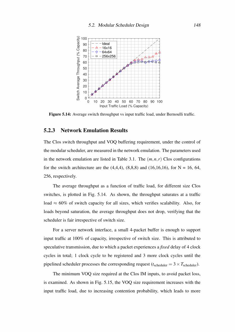
5.2. Modular Scheduler Design 148
0 10 20 30 40 50 60 70 80 90 100
Input Traffic Load (% Capacity)
0
10
20
30
40
50
60
70
80
90
100
Sw
itch
Ave
rag
e T
hro
ug
hp
ut
(% C
ap
acity)
Ideal16x1664x64256x256
Figure 5.14: Average switch throughput vs input traffic load, under Bernoulli traffic.
5.2.3 Network Emulation Results
The Clos switch throughput and VOQ buffering requirement, under the control of
the modular scheduler, are measured in the network emulation. The parameters used
in the network emulation are listed in Table 3.1. The (m,n,r) Clos configurations
for the switch architecture are the (4,4,4), (8,8,8) and (16,16,16), for N = 16, 64,
256, respectively.
The average throughput as a function of traffic load, for different size Clos
switches, is plotted in Fig. 5.14. As shown, the throughput saturates at a traffic
load ≈ 60% of switch capacity for all sizes, which verifies scalability. Also, for
loads beyond saturation, the average throughput does not drop, verifying that the
scheduler is fair irrespective of switch size.
For a server network interface, a small 4-packet buffer is enough to support
input traffic at 100% of capacity, irrespective of switch size. This is attributed to
speculative transmission, due to which a packet experiences a fixed delay of 4 clock
cycles in total; 1 clock cycle to be registered and 3 more clock cycles until the
pipelined scheduler processes the corresponding request (tscheduler = 3×Tscheduler).
The minimum VOQ size required at the Clos IM inputs, to avoid packet loss,
is examined. As shown in Fig. 5.15, the VOQ size requirement increases with the
input traffic load, due to increasing contention probability, which leads to more
5.2. Modular Scheduler Design 149
0 10 20 30 40 50 60 70 80 90 100
(a)
0
4
816x16
0 10 20 30 40 50 60 70 80 90 100
(b)
0
4
8
Log
2V
OQ
Siz
e (
Packet E
ntr
ies)
64x64
0 10 20 30 40 50 60 70 80 90 100
(c)Input Traffic Load (% Capacity)
0
4
8256x256
Figure 5.15: Minimum switch virtual output queue (VOQ) size vs. input traffic load: (a)16× 16 Clos switch, (b) 64× 64 Clos switch and (c) 256× 256 Clos switch.All VOQs at every switch input port are considered, to ensure no packet loss.
packets being buffered. At high loads, the required VOQ size decreases with switch
radix, because the packet destinations requested are uniformly distributed. That is,
the probability of a packet destination being requested is lower for larger switches.
For the 256×256 switch, the minimum VOQ size at 100% load is 32 packets, which
translates to 512 KB per switch input port, for 64-Byte packets. Operating the same
switch only up to the saturation load (60%), reduces the total port buffer required to
half (256 KB).
Using control backpressure, for buffering management, a small 8-packet VOQ
would suffice, irrespective of traffic load and switch size. This further reduces the
port buffer size by half (128 KB). The trade-off is that a larger FIFO queue would
be required, at every server network interface, depending on the traffic load.
5.2.4 Hardware Implementation
In this section, the implementation of the modular scheduler design, on hardware,
is discussed. Every hardware module in the scheduler, described above, has been
implemented separately, as an application-specific integrated circuit (ASIC), in a
45 nm CMOS process. For each module, the critical path is identified and the
minimum clock period is measured. The module in which the longest critical path

5.2. Modular Scheduler Design 150
Minimum Clock Period
Scheduler Module 16x16 64x64 256x256
OM Allocation 0.8 ns 1.1 ns 1.5 ns
OM Allocation - iSLIP 1.1 ns 1.4 ns 2.0 ns
OP Allocation 0.8 ns 1.1 ns 1.5 ns
Switch Configuration 0.5 ns 0.8 ns 1.1 ns
Table 5.4: Scheduler Modules Minimum Clock Period for ASIC Synthesis.
lies, determines the minimum clock period achievable, for the entire scheduler. That
particular module is then implemented on a Virtex-7 XC7V690T FPGA board, to
investigate how the modular scheduler compares to our previous designs, and also
to related work in the literature.
5.2.4.1 Application-Specific Integrated Circuit (ASIC)
The critical path, for every scheduler module, is marked in red in the corresponding
circuit diagram, in section 5.2.2. Table 5.4 lists the minimum clock period for every
scheduler module, at different switch sizes, for ASIC implementation. The longest
critical path is in the OM allocation module, for switch VOQ packets. It falls in
the first pipeline stage responsible for iSLIP allocation. It extends from the request
register through a cascade of two iSLIP arbiters and then back to the priority register
of the first arbiter, as shown in Fig. 5.9. This module sets the minimum clock period,
Tscheduler, for the entire scheduler. For a 256×256 Clos switch, Tscheduler = 2.0 ns.
According to Table 5.4, the increase in minimum clock period, as the switch
quadruples in size, is sublinear for all scheduler modules, demonstrating a scalable
scheduler design. The OM allocation module for new packets and the OP allocation
module, use same size arbiters, request and grant logic, hence the critical path is
of the same length. Moreover, there is only a small difference in minimum clock
period between the different scheduler modules, for the same switch size, indicating
an overall pipelining balance in the scheduler design. As shown in Fig. 5.5, the
entire scheduler design can be implemented as a 3-stage pipeline, in which case the
total scheduler delay, for a 256×256 switch, would be tscheduler = 3Tscheduler = 6 ns.

5.2. Modular Scheduler Design 151
Minimum Clock Period
Scheduler Module 16x16 64x64 256x256
OM Allocation - iSLIP 2.9 ns 4.5 ns 7.0 ns
Table 5.5: Scheduler Minimum Clock Period for FPGA Implementation.
5.2.4.2 Field-Programmable Gate Array (FPGA)
The critical path in a digital design is the same, irrespective of the hardware platform
onto which the design is implemented. The length of the critical path, however, does
vary with hardware platform. More specifically, a design runs faster as an ASIC,
than on an FPGA. In order to enable a fair comparison between the modular Clos
scheduler and other scheduler designs, the minimum clock period of the modular
Clos scheduler, in an FPGA implementation, is measured. To do so, only the OM
allocation module, for IM VOQ packets, needs to be implemented, as in this module
lies the longest critical path that determines the clock speed for the entire scheduler.
Table 5.5 lists the module’s minimum clock period, for different switch sizes,
for implementation on the Xilinx Virtex-7 XC7V690T FPGA board. As the switch
quadruples in size, the minimum clock period again shows a sublinear increase,
which verifies the scheduler is also scalable in an FPGA implementation. Compared
to the timing results for the ASIC OM allocation module (iSLIP), in Table 5.4, the
same module runs considerably slower on the FPGA. The ASIC improvement is
higher for larger switches; the ASIC scheduler runs 2.6 times faster for N = 16 and
3.5 times faster for N = 256. A delay comparison to different scheduling approaches
in the literature, is presented in section 5.2.5.1.
5.2.4.3 Packet Latency
The packet latency, using the modular Clos scheduler, was measured in the network
emulation and translated into absolute time, using the ASIC implementation results
presented above (Table 5.4).
For the packet latency results in this section, a synchronous control plane is
assumed (tsync = 0), therefore tscheduler = 3Tscheduler. At a network interface, for
the head-of-line packet in the FIFO queue, the time to generate the request is

5.2. Modular Scheduler Design 152
Minimum
Switch Size Packet Latency (ns)
16×16 26.3
64×64 27.8
256×256 30.8
Table 5.6: Minimum End-to-End Packet Latency vs. Switch Size.
treq = 2Tscheduler. The 64-byte packets are wavelength-striped across 8 wavelengths
channels, at a 100 Gb/s channel bit rate, giving tserial = 0.64 ns. Substituting the
fixed delays for propagation (tpropagation) and switch reconfiguration (tswitch), from
Table 3.2, into Equations 3.3 and 3.5, the minimum packet latency (tqueue = 0) is
calculated and listed in Table 5.6. For the 256× 256 Clos switch, the minimum
packet latency is 30.8 ns, out of which 20 ns is due to a 2×2 m propagation delay.
Clock and data recovery (CDR) at the receiver is excluded but the overhead will not
be significant, given the sub-nanosecond CDR time reported in [108].
Next, the packet latency distribution is examined. Figure 5.16 shows the packet
latency CDF, for 16≤ N ≤ 256 Clos switches, at 25%, 50% and 75% traffic loads.
At a 25% load (Fig. 5.16a), more than 20% of the packets are delivered with the
minimum latency, for all switch sizes. As the load is increased to 50% (Fig. 5.16b)
and 75% (5.16c), the percentage of minimum latency packets drops, as it becomes
increasingly difficult for new packets to pass through the 3-condition filter, in the
scheduler switch configuration module (section 5.2.2.4). This filter ensures strict,
in-order packet delivery and low average latency. The median packet latency is well
below 100 ns, at least up to a 50% load. At 75% load, the switch is operated beyond
saturation. The median latency is considerably increased and latency in general is
more variable, for all sizes. The CDF 99% to 100% tails, for all sizes and loads
investigated, have a latency range less than an order of magnitude, as shown in the
insets in Fig. 5.16.
Figure 5.17 shows the average packet latency against input traffic load, for
different size Clos switches. At low loads, the average latency converges to the
minimum value, for all switch sizes. The latency is fairly constant up to a 50%

5.2. Modular Scheduler Design 153
101 102 103 1040
0.1
0.2
0.3
0.4
0.5
0.6
0.7
0.8
0.9
1
(a)
Cu
mu
lati
ve
Pro
bab
ilit
y
16x1664x64256x256
0 50 1000.99
1
101 102 103 1040
0.1
0.2
0.3
0.4
0.5
0.6
0.7
0.8
0.9
1
(b)
Cu
mu
lati
ve P
rob
ab
ilit
y
0 500 1000 15000.99
1
101 102 103 104
Packet End-to-End Latency (ns)
0
0.1
0.2
0.3
0.4
0.5
0.6
0.7
0.8
0.9
1
(c)
Cu
mu
lati
ve
Pro
ba
bil
ity
0 4000 80000.99
1
Figure 5.16: Cumulative distribution of the packet end-to-end latency at (a) 25%, (b) 50%and (c) 75% input traffic loads, for different size Clos switches, and ASICscheduler. Network model assumes SOA-based Clos switch with a 2 m linkdistance to every source and destination. Packets are 64 B, wavelength-stripedat 8×100 Gb/s and injected based on a Bernoulli process.

5.2. Modular Scheduler Design 154
0 10 20 30 40 50 60 70 80 90 100
Input Traffic Load (% Capacity)
101
102
103
104
Av
era
ge
En
d-t
o-E
nd
La
ten
cy
(n
s)
16x1664x64256x256
Figure 5.17: Average end-to-end latency vs. input traffic load, for different size Closswitches, and ASIC scheduler. Network model assumes SOA-based Closswitch with a 2 m link distance to every source and destination. Packets are64 B, wavelength-striped at 8× 100 Gb/s and injected based on a Bernoulliprocess.
load, with a small increase for the larger switches. For latency less than 100 ns,
there is only a 5% decrease in maximum load, per 4-fold increase in switch size,
indicating scalability. The 256× 256 switch has a nanosecond average latency up
to an 80% traffic load.
5.2.5 Switch Design Comparison
5.2.5.1 Scheduling
Notable approaches to optical packet switch scheduling, from various research labs
in the field, are reviewed in this section. The switch architecture is important as
it could simplify scheduling and reduce its delay. At the same time, it should not
require many optical components, hindering implementation. Scheduling can be
executed centrally or in a distributed fashion, with the former usually considered
to be of high complexity and incurring a considerable delay. The aim here is to
show otherwise. In some approaches the packet header/request is optical and in
others electrical. Also, some switches use ACK signalling, to avoid buffering in the
switch. Table 5.7 compares the different scheduling approaches and their benefits
and shortcomings are discussed.
SPINet [11], distributes scheduling to the 2×2 modules in an N×N banyan-

5.2. Modular Scheduler Design 155
Scheduling Delay (ns)Switch N=16 N=32 N=64 N=256 Method Request ACK
Clos-MDLR 3.3 - 4.2 6.0 Central Electrical No(ASIC)
Clos-MDLR 8.7 - 13.5 21.0 Central Electrical No(FPGA)
Clos-GLBL - 16.2 - - Central Electrical No(FPGA)AWGR- 17.0 17.0 17.0 - Distributed Optical YesLION
Banyan- 20.0 25.0 30.0 40.0 Distributed Optical YesSPINetSpanke- 25.0 25.0 25.0 - Distributed Optical Yes
OPSquareCrossbar- - - 51.2 - Central Electrical YesOSMOSIS
Table 5.7: Scheduling Comparison
topology switch architecture. It scales by cascading log2(N) internal stages.
Scheduling per module is executed in 5 ns [87] but cascading them in many stages
increases total scheduling delay (log2(N)×5 ns) and limits the switch throughput.
The OPSquare wavelength-routed switch [21, 95, 94] is also modular and
scales by stacking modules in a 2-stage Spanke architecture and by increasing
the wavelength channels. It avoids arbitration for the output modules by using
wavelength conversion. The arbitration time for the input modules depends on
the wavelength-count, bringing the total scheduling delay to 25 ns, independent
of switch size. However, wavelength conversion and the high optical components
count increase the implementation complexity and cost.
All aforementioned designs use optical request schemes, therefore have
scheduling overheads for optical filtering, O/E conversion and request detection,
in addition to arbitration. The LION switch [98] avoids these overheads because it
uses optical instead of electronic scheduling. Also, it is based on an N×N AWGR,
whose scaling is limited by the number of wavelengths supported by the AWGR
technology. Optical scheduling is distributed to the output ports [109], by using

5.2. Modular Scheduler Design 156
reflective semiconductor optical amplification (RSOA) for nanosecond arbitration
[99], independent of switch size. Scheduling delay is limited by laser tuning time
(8 ns), necessary for wavelength routing, and switch round-trip time (5 ns) and
grant detection time (4 ns) at the source, due to output-port grant acknowledgement
(ACK) prior to packet transmission [99]. Also, RSOA-based arbitration fairness, is
not as strong compared to electronic round-robin schemes.
The central scheduler in the OSMOSIS prototype [12] uses a parallel iterative
scheduling algorithm [90], to improve throughput in a crossbar switch, at the cost of
high scheduler complexity and delay. To schedule a 64×64 crossbar, the OSMOSIS
scheduler requires 51.2 ns [12]. Moreover, as already discussed, an N×N crossbar
is not practical for photonic integration at large sizes, due to the N2 switch elements
required to build it.
All designs that use ACK signalling, from the switch back to the packet source,
whether in an optical or electrical form, incur control overheads for ACK transport,
detection and processing at the source, in addition to scheduling.
The proposed switch design uses a 3-stage Clos architecture and a parallel
modular scheduler design (Clos-MDLR). The Clos switch modules use broadband
SOA gating elements, in the broadcast-and-select configuration. In comparison to
OPSquare, the low component count and lack of wavelength conversion, simplifies
architecture and allow for switch photonic integration. Using electrical requests,
eliminates all scheduling overheads for request detection, present in the SPINet and
OPSquare designs. Speculative packet transmission and buffered switch, eliminate
the round-trip and grant detection overheads in the proposed design, as grant/ACK
signalling is not used. Also, the proposed space switch avoids the wavelength tuning
overhead in scheduling wavelength-routed switches, such as the LION switch. Non-
iterative, modular arbitration and a novel Clos routing scheme, enable scheduling a
256× 256 switch in 6.0 ns, in an ASIC implementation, or in 21.0 ns in an FPGA
implementation, outperforming the best designs in the field, including our global-
arbitration Clos scheduler (Clos-GLBL).

5.2. Modular Scheduler Design 157
0 10 20 30 40 50 60 70 80 90 100
Input Traffic Load (% Capacity)
0
10
20
30
40
50
60
70
80
90
100
Sw
itch
Ave
rag
e T
hro
ug
hp
ut
(% C
ap
acity)
64x64-LION
256x256-Clos-MDLR
4x4-OPSQUARE
64x64-SPINET
32x32-Clos-GLBL
Figure 5.18: Switch average throughput vs. input traffic load, for different switch designs,under Bernoulli traffic.
5.2.5.2 Switch Throughput and Packet Latency
The switch latency and throughput performance is compared to SPINet, OPSquare
and LION optical switches, as well as our global-arbitration Clos scheduler, under
Bernoulli traffic.
The average switch throughput is expressed as a percentage of output capacity,
hence different switch designs can be compared irrespective of their port count (N).
As shown in Fig. 5.18, our Clos-GLBL switch design, saturates at 32% of capacity.
The SPINet banyan switch saturates at 65% of capacity when a speedup factor of
2 is used [11], thus the effective input traffic load is only 32.5%. Both Clos-GLBL
and SPINet perform poorly, due to their blocking routing scheme. The non-blocking
OPSquare switch, saturates at approximately 50% of capacity [95]. The proposed
Clos-MDLR outperforms all three, saturating at a load 60% of capacity, despite
its blocking routing algorithm. The performance improvement is due to the VOQ
buffering scheme, at the switch inputs, which reduces the packet HOL blocking.
The LION switch [99], based on a non-blocking, wavelength-routed architecture,
saturates at 75% of capacity. The throughput gain in the LION switch is mainly due
to using 4 receivers per output port, which allows up to 4 packets being delivered in
the same clock cycle, on different wavelengths.

5.2. Modular Scheduler Design 158
0 10 20 30 40 50 60 70 80 90 100
Input Traffic Load (% Capacity)
101
102
103
104
105
Avera
ge
En
d-t
o-E
nd
Late
ncy (
ns)
31%
64x64-LION
256x256-Clos-MDLR
4x4-OPSQUARE
64x64-SPINET
32x32-Clos-GLBL
Figure 5.19: Average end-to-end packet latency vs. input traffic load, for different switchdesigns. Clos-MDLR/GLBL latency is based on scheduler implementation onthe Virtex-7 XC7V690T FPGA board. The network model assumes a 2 m linkdistance to every source and destination. Packets are 64 B and injected basedon a Bernoulli process.
For a fair packet latency comparison, the FPGA-based scheduler is assumed in
the latency calculation. As already discussed, the scheduler runs slower on an FPGA
than it does as an ASIC. For a 256×256 switch, the FPGA scheduler has a minimum
clock period (Tscheduler) of 7.0 ns, contributing a total scheduling delay of tscheduler =
3×7.0 = 21.0 ns, in the latency calculation. For consistency with the other designs,
the bit rate (Rb) assumed is reduced from 100 Gb/s to 10 Gb/s, increasing the packet
(de)serialisation delay (tserial) to 3.2 ns, assuming 16 wavelength channels (k = 16).
The packet latency for the 4× 4 OPSquare [95] and the 64× 64 LION [99]
switches has been reduced, to account for only a 2 m distance between switch and
network nodes. A 51.2 ns packet serialisation delay has been added to the OPSquare
latency, for 64 B packets serialised at 10 Gb/s onto a single wavelength. The latency
for LION, OPSquare, SPINet and Clos-MDLR, includes the scheduling delay listed
in Table 5.7. For a 64× 64 SPINet [11], only a minimum latency comparison is
carried out. This includes packet serialisation, a round-trip to the switch output port
(ACK signalling) and the total scheduling delay.
In Fig. 5.19, the average packet latency for a 256-port Clos switch, using the

5.3. Summary 159
proposed modular scheduler (Clos-MDLR), is compared to the other designs. Clos-
MDLR achieves a sub-microsecond average packet latency up to a 65% traffic load.
This represents a 31% increase, for a switch size 8 times larger, compared to the
32×32 Clos-GLBL. For the minimum latency in a 64-port SPINet, the Clos-MDLR
can support 10% more traffic, for a switch 4 times larger. Clos-MDLR outperforms
the 64× 64 LION switch, for all reported traffic loads (up to 65%), also for a 4-
fold increase in switch size. Against the small 4×4 OPSquare switch, the 256-port
Clos switch achieves a lower latency, up to 55% traffic load. It should be noted,
however, that OPSquare drops packets and does not consider contending packets
that are re-transmitted more than once.
5.3 Summary
A three-stage (m,n,r) Clos network, in certain topological configurations, has been
shown to be a practical switch architecture for scalable photonic-integrated packet
switching. In this chapter, two scheduler designs for Clos switches were presented.
In the first design, output ports are allocated globally by considering requests
from all input ports, similar to a crossbar scheduler. In this way, however, the Clos
scheduler could never run faster than a crossbar scheduler, as it is limited by the
N-bit arbiter in the critical path. Implementation of the global Clos scheduler, on
the Xilinx Virtex-7 XC7VX690T FPGA, gave 5.4 ns minimum clock period against
5.0 ns for a crossbar scheduler, for a 32×32 switch size. Unlike a crossbar, a Clos
switch requires a routing scheme. In order to execute routing in a single clock cycle,
a random path assignment was used. In total, the Clos scheduler takes 3 clock cycles
to reconfigure the switch, compared to two clock cycles for the crossbar scheduler,
due to the additional pipeline stage for Clos routing. As a result, the minimum end-
to-end packet latency is 51.6 ns versus 44.6 ns for the crossbar, assuming rack-scale
distances and 64-byte packets serialised at 4× 100 Gb/s. However, using random
path assignment, the switch becomes blocking which in turn reduces the achievable
saturation throughput, compared to using the looping algorithm for re-arrangeable
non-blocking Clos networks. In a 32× 32 network emulation, the throughput for

5.3. Summary 160
a (4,4,8) Clos switch was measured and compared to that for a route-less, strictly
non-blocking crossbar, to evaluate the penalty of random routing. Results showed
a saturation throughput at 32.1% of capacity versus 62.5% for the crossbar. To
improve saturation throughput, using a Clos network with m = 2n was proposed,
so that the probability of contention for a random path is lower. The (8,4,8) Clos
was implemented on the same FPGA achieving the same minimum clock period
(5.4 ns), and hence the same minimum packet latency as the (4,4,8) Clos switch.
Network emulation results showed a saturation throughput at 47.5% of capacity,
representing only a 15% routing penalty compared to the crossbar.
In the aforementioned switch design, the global Clos scheduler can never run
faster than a crossbar scheduler and requires that the switch uses at least twice as
many central modules, for satisfactory throughput performance, making the switch
less practical for photonic integration at large sizes. To this end, a second scheduler
for Clos switches with m = n = r =√
N was designed. It reconfigures the switch
based entirely on distributed path allocation for the modules in the Clos switch. The
significance of this is that only a√
N-bit arbiter is in the critical path, allowing for
a considerably shorter minimum clock period, compared to a crossbar scheduler.
To keep the scheduling delay to three clock cycles, a fixed path assignment is used
to eliminate contention at the Clos central modules for output modules. Therefore,
no extra pipeline stage is needed for output module arbitration. As with random
routing, fixed path assignment makes the switch architecture blocking. In order
to improve throughput, virtual output queue (VOQ) buffering at the switch inputs
was proposed. The distributed path allocation allowed designing the scheduler in a
modular fashion and then optimising those modules for clock speed. Each scheduler
module was synthesised as an ASIC in a 45 nm CMOS process and the critical path
module was identified. This was the module that performs iSLIP allocation for VOQ
requests, for a Clos input module, achieving a minimum clock period of 2.0 ns, for
a 256× 256 Clos switch. For design comparison, the critical path module was
implemented on the Xilinx Virtex-7 XC7VX690T FPGA, giving a minimum clock
period of 7.0 ns, for the 256× 256 Clos switch. This result verifies a significant

5.3. Summary 161
scalability improvement over the global Clos scheduler, which achieves a minimum
clock period of 5.4 ns for a 32× 32 Clos switch. Moreover, the total scheduling
delay for the modular Clos scheduler is 3×7.0 = 21.0 ns, which is lower compared
to state-of-art switch designs in the literature, namely the LION, OPSquare, SPINet
and OSMOSIS.
The average switch throughput and packet latency were measured and also
compared to other switch designs, in the network emulation. Under control of the
modular Clos scheduler, the switch throughput saturates at 60% of capacity, which
is approximately double the one under global scheduler control or for the SPINet
switch, and 10% higher compared to OPSquare. The LION switch saturates at 75%
of capacity by using 4 times as many receivers per output port. Furthermore, the
modular scheduler enables a 256× 256 Clos switch to achieve a sub-microsecond
average packet latency up to a 65% traffic load. This is approximately 30% higher,
compared to using the global Clos scheduler, for a switch size eight times larger.
The modular scheduler allows the 256-port Clos switch to outperform the LION,
OPSquare, SPINet and OSMOSIS switches, despite its much larger size.
Although it is suggested that the proposed optical switch is used to replace
electronic top-of-rack switches in the leaf network layer, the demonstrated 256-port
Clos switch is large enough for application at the spine layer.

Chapter 6
Experimental Demonstration
The control plane, in the proposed system concept, is experimentally demonstrated
in an FPGA-based implementation. It includes two server-side network interfaces
and a crossbar scheduler, implemented on different FPGA boards. The components
in the control delay and packet latency are identified. The control plane is then used
to demonstrate nanosecond optical packet switching, in a laboratory setup, and the
minimum end-to-end packet latency is measured. The limitations on the minimum
packet latency and the significance of control plane synchronisation, are discussed.
A balanced pipeline scheduler design is then implemented on the same FPGA board
as the experimental scheduler, to quantify delay reduction and assess scalability.
In our network emulation, the packet latency for the two crossbar schedulers is
measured and compared to one another. The work reported here was reviewed and
published in [29, 30].
6.1 Control Plane Components
6.1.1 Server Network Interface
Every packet a server injects is first buffered in a first-in, first-out (FIFO) queue, in
the network interface (NI). When the queue is not empty, the Request Control reads
the destination of the head-of-line (HOL) packet and issues an output port request
to the scheduler. After a configurable delay, tstx, the Packet Control forwards the
HOL packet to the transmitter (TX), speculatively; it does not wait for an output
port grant from the scheduler. Therefore, the network interfaces “send and forget”

6.1. Control Plane Components 163
packets, as opposed to storing them for possible re-transmission. The tstx delay is a
configurable number of clock cycles, where a network interface clock cycle is Ttx,
to ensure the HOL packet reaches the switch as soon as it has been reconfigured.
At the TX, the packet is divided and serialised onto k parallel wavelength channels,
with each channel running at a bit rate Rb. In this demonstration, the packet size
is 64 bytes, k = 8 and Rb = 10 Gb/s, giving a serialisation delay (tserial) of 6.4 ns.
Also, for a 32× 32 switch, the request structure consists of a 5-bit port field, to
address each output port, and a valid bit. The Request Control extends the duration
of a request, by a configurable number of clock cycles, so that a scheduler running
at a lower clock speed can detect them.
The constraints on the minimum Ttx, are due to the bit rate per lane (Rb) on
the wavelength-striped data path and the width of the parallel bus that drives the
serialiser. For this demonstration, 10 Gb/s per lane and a 32-bit parallel bus give
Ttx = 32 bits/10 Gb/s = 3.2 ns. Two network interfaces were implemented onto the
Xilinx Virtex-7 XC7VX690T FPGA board, with this clock constraint.
6.1.2 Switch Scheduler
The switch scheduler receives requests from the server network interfaces, performs
output port allocation, resolves any contention for output ports and reconfigures the
switch. In this demonstration, the scheduler design is a two-stage pipeline, hence
the total scheduling delay is fixed to two clock cycles, where a scheduler clock cycle
is Tscheduler.
The circuit design for the experimental scheduler is illustrated in Fig. 6.1. The
circuit has two input request matrices, one for new server requests (R) and one for
switch buffer requests (RS). Every matrix holds up to N valid requests, where each
request has a port field of log2(N) bits, to address the destination output port, and
a valid bit to indicate the request presence. In the first pipeline stage, the two input
request matrices are processed in parallel, by a dedicated Arbiter Request logic, to
generate the request vectors for the arbiters. Every vector has N bits to indicate the
requesting input ports, for a specific output port, that an arbiter will handle next.
In the second pipeline stage, the Request MUX logic gives input port priority, for

6.1. Control Plane Components 164
Re
qu
est
MU
X
log2(N)+1
/Allocator
Arbiter
0
Arbiter
1
Arbiter
N-1
Grant
Switch
Config.
Read-
Enable
Write-
Enable
/
/
/
/
N/
N
N
N
N
Arb
ite
r R
eq
ue
st
log2(N)+1
log2(N)+1
/N
Arb
ite
r R
eq
ue
st
R
/
RS
CCNFG
CRE
CWE
G
/
1st
Stage:
Arbiter Requests
2nd
Stage:
Output-Port Allocation & Switch Configuration
Figure 6.1: Scheduler design with 2-stage pipeline for an N×N crossbar switch. Criticalpath shown in red.
an output port request, to packets buffered at the switch, for strict in-order packet
delivery. The logic also receives feedback from the Grant register, to remove any
requests that have already been granted. Next, output-port allocation takes place,
based on round-robin arbitration. The arbiter grants are forwarded to parallel logic
blocks for generating the circuit outputs; the N-bit grant vector (G), the N-bit write-
enable (CWE) and read-enable (CRE) vectors, for the buffers at the switch inputs, and
the switch configuration matrix (CCNFG). In the latter, every signal has a port field
of log2(N) bits, to address a switch element (SOA), and a valid bit.
The feedback, from the Grant register to the Request MUX logic, forms the
critical path in the design. It extends from the Grant register, through one of the
arbiters and back to the Grant register itself, as marked in Fig. 6.1. For the 32×32
crossbar, in this demonstration, the minimum Tscheduler achievable on the Xilinx
Kintex-7 XC7K325T FPGA board, is 9.6 ns.
6.1.2.1 Metastability Resolution
In the experiment, to avoid clock distribution, the FPGA boards onto which the
control plane is implemented, are ran from independent crystal oscillators, hence

6.1. Control Plane Components 165
they are asynchronous. As discussed above, the FPGA board onto which the server
network interfaces are implemented, runs at a 3.2 ns clock period. The FPGA board
for the scheduler, runs at a 9.6 ns clock period.
At the scheduler, since the input requests are asynchronous, it is possible that
a request arrives just as the clock rises. This may result in a phenomenon called
metastability, whereby the input flip-flop, in the first pipeline stage, captures a value
midway between a logic 0 and a logic 1. The flip-flop is said to be in a metastable
state and will, eventually, resolve the output to a stable state of either a logic 1
or a logic 0. The time, however, required until the output settles to that state, is
unbounded. This could cause an erratic scheduling failure that would be difficult to
detect and correct.
A synchronisation circuit, or synchroniser, can be used to significantly reduce
the probability of a flip-flop entering metastability. A synchroniser is a device that
receives an asynchronous input bit (D) and a clock signal (clk), and outputs a bit (Q)
that is either equal to D, if D does not arrive as clk rises, or equal to a logic 0 or 1.
Q settles to its final value within a bounded amount of time. A simple synchroniser
can be built as a cascade of two flip-flops, with no other logic in between. In case
the synchroniser input D changes as the clock changes, the output of the first flip-
flop D1 may be momentarily metastable. However, given the clock period is long
enough, D1 will most probably resolve to a valid state, before the period ends. The
second flip-flop will then sample a stable D1, generating a valid output Q.
Every input request bit has to pass through such a synchroniser, before entering
the scheduler. Both the scheduler and all preceding synchronisers are implemented
on the same FPGA board (Xilinx Kintex-7 XC7K325T). It is uncertain when a
request arrives, with respect to the scheduler clock edge, giving rise to a variable
synchronisation delay, tsync. In the best case, the request is aligned in time with the
clock edge, giving tsync = 1Tscheduler. In the worst case, the request arrives just after
the clock edge, giving tsync = 2Tscheduler. Therefore, 1Tscheduler ≤ tsync ≤ 2Tscheduler.
In this chapter, this phenomenon is referred to as synchronisation uncertainty.

6.2. Experimental Setup 166
FPGA#2FPGA#1
SWITCH
NETWORKINTERFACE
RE
QU
ES
T
CO
NT
RO
LL
ER
PA
CK
ET
CO
NT
RO
LL
ER
RE
QU
ES
T
TX
PACKET
TX
PACKET
TX
PA
CK
ET
GE
NE
RA
TO
R
D0
D1
D2
SOA 1
SOA 2
D3
SOA 0
SOA 3
RE
QU
ES
T
SY
NC
HR
ON
IZE
R
AL
LO
CA
TIO
N
SW
ITC
H
CO
NF
IGU
RA
TIO
N
N-1
01
RX
RXD4
D5
D7
D6
N2 -
10
2m
2m
2m
REQUESTS
PACKETS
PACKETS
3.2ns 6.4ns 10ns 10ns
3.2ns 10ns 19.2ns 19.2ns 3ns
2m
2m
3.2ns 10ns 19.2ns 19.2ns 3ns
t CONTROL (MIN)
t END-TO-END (MIN)
t DATA (MIN)
10ns 6.4ns = 71ns
-D0
D7 OSCILLOSCOPE PROBES
-C0
C6 XILINX ILA PROBES1
2
CONTROL PATH
DATA PATH
Figure 6.2: The experimental setup. Control path and data path latency contributions andthe minimum end-to-end latency are marked on the figure. Oscilloscope probesD0-D7 are placed along the data path. Xilinx Integrated Logic Analyzer (ILA)probes C0-C6 are implemented onto the scheduler FPGA board.
6.2 Experimental Setup
Figure 6.2 shows the setup for the control plane demonstration. It includes two
FPGA boards and an SOA-based 2×2 optical crossbar, built out of discrete optical
components. FPGA#1 is a Xilinx Virtex-7 XC7VX690T board and implements two
server-side network interfaces. It runs at a clock period Ttx = 3.2 ns, as described in
section 6.1.1. FPGA#2 is a Xilinx Kintex-7 XC7K325T board and implements the
scheduler, including synchronisers. It runs at a clock period Tscheduler = 9.6 ns, as
described in section 6.1.2.
The SOA devices used in the setup are from the Centre for Integrated Photonics
(CIP) with part number SOA-NL-OEC. They have a reconfiguration time, tswitch,
of approximately 3 ns. The cabling length in the control path, as well as in the
data path from the server network interfaces to the switch/scheduler and from the
switch/scheduler to the optical receivers, was kept as close to 2 m as possible, to
represent the case for a top-of-rack (ToR) switch application. For this cable length,
the propagation delay, tpropagation, is 10 ns.
Given the control plane design and minimum achievable packet latency are the
main focus, the data plane was simplified in the following ways:

6.2. Experimental Setup 167
1. Although the crossbar scheduler was fully implemented for a 32×32 switch
size, only a 2×2 crossbar was implemented in the setup.
2. Since minimum latency occurs under no contention, no buffers were used at
the crossbar inputs. The scheduler still generates the buffer control signals.
3. A single-wavelength 10 Gb/s optical transceiver, per network interface,
was used and only 64 bits per packet were transmitted, to emulate 64 B
wavelength-striped packets transmitted at 8×10 Gb/s.
On FPGA#1, in addition to the two network interfaces and optical transceivers,
a packet generator has been implemented. The generator, periodically constructs
64-byte packets, representative of the smallest Ethernet packet size, for which the
minimum end-to-end latency occurs. A linear feedback shift register is used to
assign a pseudo-random payload to the packets. In each network interface, the
Request Control generates 6-bit requests, including the port field and valid bit, for
a 32-port switch. The port field, addresses only the two output ports in the partially
implemented crossbar, in the setup. The request duration is set to 4Ttx = 12.8 ns, for
the slower scheduler to detect them. The requests are transported to the scheduler
FPGA board in a bit-parallel format, over electrical lines (tpropagation = 10 ns). The
delay before speculative packet transmission, tstx, is set to 10Ttx = 32 ns to account
for the total scheduling delay and additional fibre delays in the discrete-component
setup (splitters/combiners, receivers).
On FPGA#2, the scheduler output signals, for switch reconfiguration, are held
for an additional clock cycle. This is to accommodate both tserial and tswitch, and
also to account for the synchronisation uncertainty, as described below. A Xilinx
Integrated Logic Analyzer (ILA) core is also implemented on FPGA#2, for real-
time monitoring of the internal scheduler signals, using probes C0-C6 as marked in
Fig. 6.2.
The control plane extends across both FPGA boards; it includes the Request
Control and Packet Control, in the network interfaces (FPGA#1) and the scheduler
(FPGA#2). The control plane delay is therefore given by the sum of the individual

6.2. Experimental Setup 168
control processes, taking place on the two FPGA boards:
1. Request generation: The Request Control reads the destination of the HOL
packet and generates a request. The delay, treq, is equal to 1Ttx.
2. Propagation delay: The request is transported to the scheduler out-of-band,
on parallel electrical wires. The delay, tpropagation, is determined by the wire
length between the server and the scheduler.
3. Request synchronisation: The request synchroniser has a worst case delay,
tsync, of 2Tscheduler, when the request arrives just after the clock edge.
4. Scheduling: The scheduler performs output port allocation and generates the
new switch configuration, including the buffer control signals for the switch.
The total scheduling delay, tscheduler, is 2Tscheduler.
5. Switch reconfiguration: The time tswitch needed to switch “on” a single SOA.
This is 3 ns for the SOAs used in the setup.
The control plane delay, tcp, is calculated by adding the above components, for
the worst-case request synchronisation delay:
tcp = treq + tpropagation + tsync + tscheduler + tswitch
= 4Tscheduler +Ttx + tpropagation + tswitch
At a network interface, since the control plane delay is known, the delay before
a packet is speculatively transmitted, tstx, is set accordingly, so that a packet reaches
the switch as soon as it is reconfigured. If the scheduler has allocated that packet the
requested output port, the packet is switched with minimum latency. Therefore, the
minimum packet latency is also known and it is given by the following equation:
tpacket = tcp + tpropagation + tserial
The tpropagation term, in the packet latency calculation, refers to the packet time-
of-flight on the optical fibre, from the switch to the optical receivers. The tserial term,
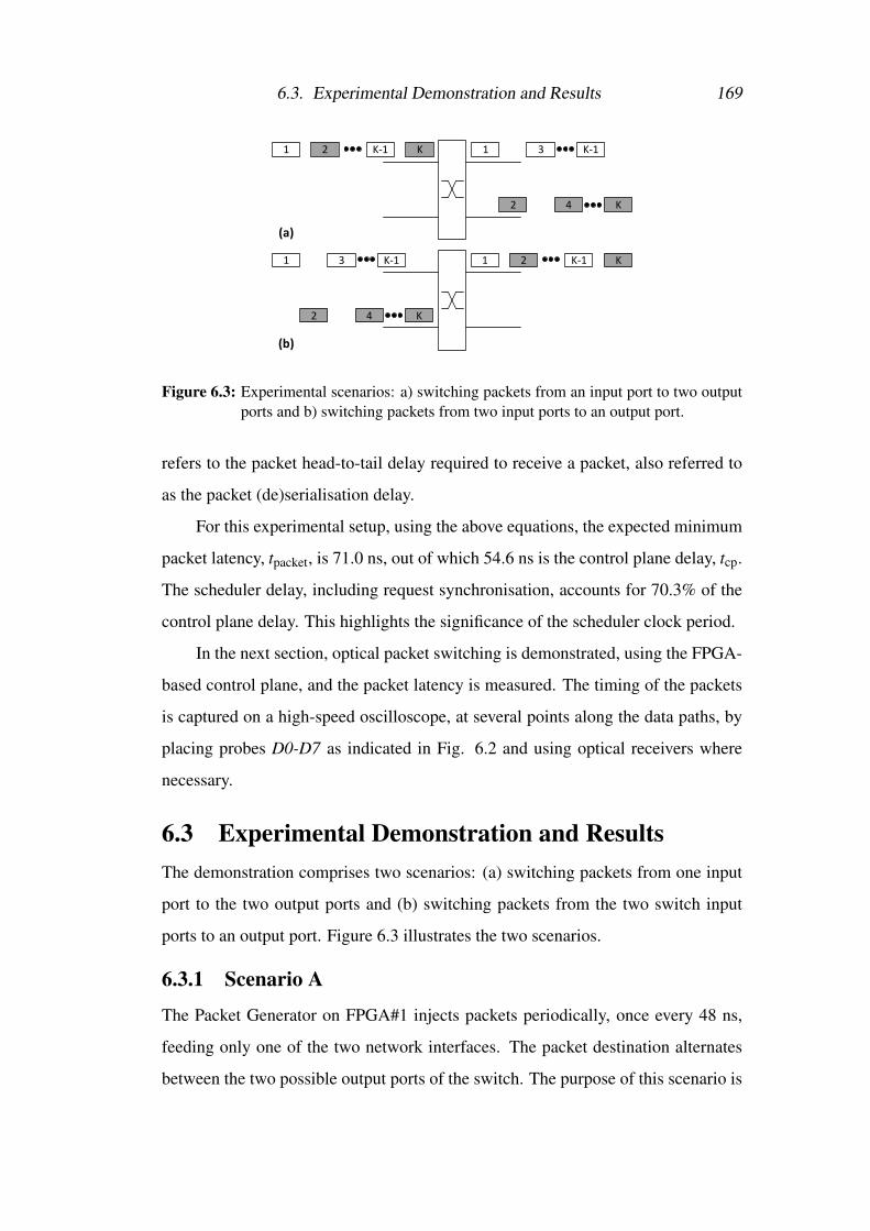
6.3. Experimental Demonstration and Results 169
K-11 2 K
1
2
3
4
K-1
K
K-11 2 K
(a)
(b)
1
2
3
4
K-1
K
Figure 6.3: Experimental scenarios: a) switching packets from an input port to two outputports and b) switching packets from two input ports to an output port.
refers to the packet head-to-tail delay required to receive a packet, also referred to
as the packet (de)serialisation delay.
For this experimental setup, using the above equations, the expected minimum
packet latency, tpacket, is 71.0 ns, out of which 54.6 ns is the control plane delay, tcp.
The scheduler delay, including request synchronisation, accounts for 70.3% of the
control plane delay. This highlights the significance of the scheduler clock period.
In the next section, optical packet switching is demonstrated, using the FPGA-
based control plane, and the packet latency is measured. The timing of the packets
is captured on a high-speed oscilloscope, at several points along the data paths, by
placing probes D0-D7 as indicated in Fig. 6.2 and using optical receivers where
necessary.
6.3 Experimental Demonstration and ResultsThe demonstration comprises two scenarios: (a) switching packets from one input
port to the two output ports and (b) switching packets from the two switch input
ports to an output port. Figure 6.3 illustrates the two scenarios.
6.3.1 Scenario A
The Packet Generator on FPGA#1 injects packets periodically, once every 48 ns,
feeding only one of the two network interfaces. The packet destination alternates
between the two possible output ports of the switch. The purpose of this scenario is

6.3. Experimental Demonstration and Results 170
(SOA 0)(SOA 2)
20100
1
42
3
1 2 3 4 5
5
48 ns/div
Figure 6.4: Scheduler shown allocating the two switch output ports in turn, one at a time,to the requesting server network interface. Traces are labelled according to theprobe placement shown in Fig. 6.2. Each subdivision is 1Tscheduler.
to demonstrate successful packet switching, for the proposed system concept, and
measure the minimum packet latency.
6.3.1.1 Control Path Signals
Figure 6.4 shows the internal scheduler signals, as captured by the Xilinx ILA core
implemented on the same FPGA board. Each trace is labelled according to the
probe used. The probe placement is as indicated in Fig. 6.2. As shown, the request
(only the valid bit is shown) successfully arrives on the scheduler board (probe
C0). The request width is 2Tscheduler, so that the following synchroniser can detect
the request. The scheduler registers the request 2Tscheduler later (probe C2), due to
the request synchronisation delay, tsync. The scheduler takes tscheduler = 2Tscheduler
to perform output port allocation and generate the new switch reconfiguration. A
reconfiguration pulse is issued to the appropriate SOA (probe C4 or C6). The width
of a reconfiguration pulse is 2Tscheduler, to accommodate both tswitch = 3.0 ns and
tserial = 6.4 ns, accounting also for the request synchronisation uncertainty.
As shown in Fig. 6.4, only one SOA is active at a time, switching a packet to
the corresponding output port. The packets appear at the same output port on every
other scheduling round, as expected.
6.3.1.2 Data Path Signals
Figure 6.5 shows the packet timing along the data path to the two switch output
ports, requested in this demonstration scenario. The packet valid bit indicates the
time the packet generator injects a packet (probe D0). The falling edge of a packet’s

6.3. Experimental Demonstration and Results 171
82.4 ns
20 ns/div
Figure 6.5: Data path from a server network interface to the two switch output ports. Tracesare labelled according to the probe placement shown in Fig. 6.2. The minimumend-to-end latency measurement is marked in this Figure.
valid bit marks the beginning of the packet latency measurement. The packet is
initially buffered in the FIFO queue and, once tstx = 32 ns is up, the Packet Control
forwards it to the optical transmitter. The packet arrives at the transmitter 36 ns
later (probe D2), where it is then serialised onto the optical fibre. It then takes
tpropagation = 12 ns for the packet’s leading edge to propagate to the switch input
(probe D4) and another 28 ns to propagate through the switch to the optical receiver
(probe D7). Finally, it takes the receiver tserial = 6.4 ns to de-serialise the packet
(probe D7). In total, the minimum latency is 82.4 ns against the expected value of
71.0 ns. The extra delay is attributed to additional printed circuit board (PCB) tracks
in the control path and fibre pigtails in the discrete components, such as combiners
(switch outputs) and optical receivers, which increase tpropagation.

6.3. Experimental Demonstration and Results 172
Injected
packet
Request arriving
at allocator
Switch configuration
Packet arriving at switch
10 ns/div
Figure 6.6: Effect of request synchronisation uncertainty on the switch configuration. Theswitch configuration pulse timing is captured using a 5-second persistence onthe oscilloscope. The speculatively transmitted packet is shown arriving at theswitch SOA at the right time.
The SOA amplification effect appears as a voltage offset in the received packets
(probes D6 and D7). Although, this can be removed with an optical filter, none
is applied to show the packet arrival relative to the scheduler SOA configuration
pulse. As shown, the pulse is long enough to accommodate the packet duration.
The packet may arrive well after the relevant SOA is turned “on”, to avoid any bit
errors or packet loss due to the asynchronous control plane.
The effect of the synchronisation uncertainty on the switch configuration
is examined in Fig. 6.6. Due to 1Tscheduler ≤ tsync ≤ 2Tscheduler, the request-to-
configuration time could vary up to 1Tscheduler. The switch configuration signals
need to be broaden by at least 1Tscheduler, for error-free operation. All possible
timings of a switch configuration are captured using a 5-second persistence on the
oscilloscope, as shown in the Figure. As a result, a window of 3Tscheduler = 28.8 ns
is formed, over which no other packet may be switched to that output port. This is
the minimum guard time. The packet is shown arriving at the switch SOA at the
right time, indicating that tstx = 10Ttx = 32 ns is correct, for this experimental setup.
6.3.2 Scenario B
The Packet Generator on FPGA#1 feeds both server network interfaces, one at a
time, with a constant time difference. Also, all generated packets are destined to
the same output port. This allows investigating the minimum time spacing between

6.3. Experimental Demonstration and Results 173
1
2
3 5 7
4 6 8
1
2
3 5 7
4 6 8
20100
48 ns/div
(SOA 0)
(SOA 1)
Figure 6.7: Scheduler shown allocating one switch output port to the two requesting servernetwork interfaces, one at a time. Traces are labelled according to the probeplacement shown in Fig. 6.2. Each subdivision is 1Tscheduler.
packets, before output port contention occurs, to measure the effective port capacity.
6.3.2.1 Control Path Signals
The internal scheduler signals, as captured by the Xilinx ILA core, are shown in
Fig. 6.7. The requests issued by the two server network interfaces (probes C0 and
C1) are shown arriving at the scheduler, with a fixed 3Tscheduler = 28.8 ns difference.
The scheduler takes up to tsync = 2Tscheduler for request synchronisation (probes C2
and C3). It then takes 2Tscheduler = 19.2 ns to allocates the output port and generate
the configuration pulse (probes C4 and C5). The output port is allocated to one
network interface at a time, in a round-robin fashion.
6.3.2.2 Data Path Signals
The packet timing along the data path from each of the two server network interface
to one of the switch output ports, is shown in Fig. 6.8. The delay contributions
to the minimum packet latency (82.4 ns), for the data path to the first output port
(probes D0, D2, D4 and D6), are the same as those in Fig. 6.5. Packets from the
two servers are successfully received at the output port, one at a time, based on
round-robin priority (probe D6). The packet spacing is the minimum achievable in
this setup and it is 32 ns (probe D6). The effective port capacity is therefore only
(6.4 ns/32 ns)× 100 = 20.0% of the theoretical value (k×Rb), due to the request
synchronisation uncertainty and its effect on the switch configuration timing, as
described above. In a synchronous control plane, the effective port capacity would

6.3. Experimental Demonstration and Results 174
82.4 ns
20 ns/div
Figure 6.8: Data path from the two server network interfaces to the first switch output port.Traces are labelled according to the probe placement shown in Fig. 6.2. Theminimum end-to-end latency and packet spacing measurements are marked inthis Figure.

6.4. Balanced Pipeline Scheduler Design 175
be (6.4 ns/9.6 ns)× 100 = 66.7% of the theoretical value. The theoretical port
capacity for the proposed switch could be very high by appropriately depending on
the number of wavelength channels (k) used and the channel bit rate (Rb).
6.3.3 Asynchronous Control Plane Limitations
Based on the experimental results, it is understood that an asynchronous control
plane, although easier to implement as no clock distribution is required, it limits the
performance of the switch.
The minimum control plane delay is increased due to the request synchronisers
preceding the scheduler circuit. Due to the request synchronisation uncertainty, the
delay tsync added is 2Tscheduler, to ensure correct packet switching.
Also due to the synchronisation uncertainty, the switch configuration needs
to be extended by at least one clock cycle, resulting in 3Tscheduler time window
over which no other packet may be allocated the assigned switch paths. This can
significantly reduce the effective port capacity of the switch.
In practice, synchronisation would also be necessary at the receivers, for data
recovery. Techniques such as injection clock recovery, electronic [110, 111] or
optical [112], and source-synchronous wavelength-striped operation [113, 114], can
be used for low-latency synchronisation. For optical switch application at the leaf
network layer, there are no clock domain crossings and hence no associated delay
for these techniques.
The performance limitations due to an asynchronous control plane, highlight
the significance of the minimum scheduler clock period, Tscheduler, achievable. The
pipeline crossbar scheduler design, presented in Chapter 4, reduces the minimum
Tscheduler, improving switch performance as discussed next.
6.4 Balanced Pipeline Scheduler DesignThe scheduler design used in the experimental demonstration, although being a two-
stage pipeline, the logic delay is not balanced between the two stages. As shown
in Fig. 6.1, output port allocation and new switch configuration are both executed
in the second stage. Hence, the critical path falls in that stage, giving a minimum

6.4. Balanced Pipeline Scheduler Design 176
log2(N)
1 2 3 4 5 6
Min
imum
Clo
ck P
eriod (
ns)
0
5
10
15
20
x4
x2
42.7%
DSGN-DEMODSGN-BLNC
Figure 6.9: Minimum clock period vs. switch size, for two crossbar scheduler designs,implemented on the Xilinx Kintex-7 XC7K325T FPGA.
Tscheduler = 9.6 ns, for the Xilinx Kintex-7 XC7K325T FPGA board.
In contrast, the crossbar scheduler, presented in Chapter 4, uses a balanced
pipeline design, as shown in Fig. 4.8. Compared to the scheduler design used in the
demonstration (Fig. 6.1), the balanced design reduces the minimum scheduler clock
period, Tscheduler, in the following ways:
1. Output port allocation and new switch configuration are divided in the two
pipeline stages.
2. Output port allocation is executed independently and in parallel for new server
requests and switch buffer requests.
3. Priority logic, for switch buffer requests, is moved to the pipeline stage for
new switch configuration.
The balanced scheduler pipeline design (DSGN-BLNC) is implemented on the
Xilinx Kintex-7 XC7K325T FPGA board, for different crossbar sizes (N). In this
way, it can be directly compared to the scheduler design used in the demonstration
(DSGN-DEMO). Figure 6.9 compares the minimum clock period achievable, for the

6.5. Network Emulation Results 177
two scheduler designs, as a function of crossbar size. For a a 32×32 crossbar, the
balanced pipeline scheduler design achieves a minimum Tscheduler = 5.5 ns, against
9.6 ns for the demonstration scheduler design, representing a 42.7% reduction in
minimum clock period. For Tscheduler = 5.5 ns, the demonstration scheduler design
can be used for a crossbar four times smaller (N = 8). Moreover, the balanced
pipeline design allows scheduling a crossbar switch twice the size, for the clock
period at which the 32-port scheduler ran, in the experimental demonstration.
Using the balanced pipeline design, for the 32× 32 crossbar scheduler in the
demonstration, would give a total scheduling delay, including worst-case request
synchronisation delay, tscheduler = 4Tscheduler = 22.0 ns. Based on the equations
above, the control plane delay and minimum end-to-end packet latency, would be
tcp = 38.2 ns and tpacket = 54.6 ns, respectively.
6.5 Network Emulation Results
In this section, the two crossbar scheduler designs are compared in terms of packet
latency, measured in the developed network emulation. The synthetic workload is
based on Bernoulli packet injection and uniformly-distributed packet destinations.
The latency is translated into absolute time, using the parameters listed in Table 6.1.
The network emulation captures the latency in the demonstrated control plane,
for a 32×32 crossbar. The clock period assumed for the server network interfaces
is Ttx = 3.2 ns and for the scheduler is Tscheduler = 9.6 ns, or Tscheduler = 5.5 ns for
the balanced pipeline design. A network interface takes treq = 3.2 ns to generate
a request, for the head-of-line (HOL) packet in its FIFO queue. Once the request
reaches the scheduler, a request synchronisation delay tsync = 2Tscheduler is assumed
(worst-case). A fixed scheduling delay tscheduler = 2Tscheduler is incurred, before the
switch configuration signals are generated. The duration of a switch configuration
pulse is extended to 2Tscheduler, or 3Tscheduler for the balanced pipeline scheduler
design, due to its shorter clock period (5.5 ns). The pulse width accounts for the
request synchronisation uncertainty and accommodates the switch reconfiguration
time tswitch = 3.0 ns, for the SOAs used in the setup, and the packet (de)serialisation

6.5. Network Emulation Results 178
Parameter Value
Crossbar Size (N) 32×32
Packet Size (S) 64 Bytes
Channel Bit Rate (Rb) 10 Gb/s
Channel Count (k) 8
Ttx 3.2 ns
Tscheduler 9.6 ns, 5.5 ns
treq 1Ttx
tsync 2Tscheduler
tserial (S×8)/(k×Rb) = 6.4 ns
tswitch 3.0 ns
tpropagation 10.0 ns
Switch Configuration 2Tscheduler, 3Tscheduler
Input Traffic Load 5% - 100%
Table 6.1: Parameters for Network Emulation.
delay tserial = 6.4 ns, for 64-byte packets (de)serialised at 8× 10 Gb/s. For a 2 m
distance between switch and servers, the propagation delay is tpropagation = 10.0 ns.
Figure 6.10 shows the packet latency cumulative distribution function (CDF),
at 50% input traffic load, for the two scheduler designs. For either DSGN-BLNC or
DSGN-DEMO, more than 10% of the packets are switched with minimum latency
and the median latency is less than 140 ns. The packet latency for DSGN-DEMO
is longer and more variable, compared to DSGN-BLNC. Also, the distribution tail,
accounting for 95% to 100% of the received packets, is considerably shorter for
DSGN-BLNC. The tail length is 406.7− 219.6 = 187.1 ns for DSGN-BLNC and
886.9−378.2 = 508.7 ns for DSGN-DEMO.
The average packet latency, at all traffic loads, for the two scheduler designs,
is shown in Fig. 6.11. The DSGN-BLNC scheduler design, enables a lower average
latency at all traffic loads. For an average packet latency ≤ 100 ns, DSGN-BLNC
increases the highest supported traffic load from 35% to 50%, compared to DSGN-
DEMO. Beyond 50% traffic load, the average packet latency increases rapidly for
both scheduler designs. Nevertheless, it remains below 10 µs, even at full port

6.6. Summary 179
0 200 400 600 800 1000
Packet Latency (ns)
0
0.1
0.2
0.3
0.4
0.5
0.6
0.7
0.8
0.9
1
Cu
mu
lative
Pro
ba
bili
ty
DSGN-DEMO
DSGN-BLNC
Figure 6.10: Cumulative distribution function of packet end-to-end latency, at 50% inputtraffic load, for two different scheduler designs implemented on the XilinxKintex-7 XC7K325T FPGA. The network model assumes an SOA-based,32× 32 crossbar switch with a 2 m link distance to every connected sourceand destination. Packets are 64 bytes, wavelength-striped at 8× 10 Gb/s andinjected based on a Bernoulli process.
0 10 20 30 40 50 60 70 80 90 100
Input Traffic Load (% Capacity)
101
102
103
104
105
Ave
rag
e L
ate
ncy (
ns)
DSGN-DEMO
DSGN-BLNC
Figure 6.11: Average end-to-end packet latency vs. input traffic load, for two differentscheduler designs, implemented on Xilinx Kintex-7 XC7K325T FPGA. Thenetwork model assumes an SOA-based, 32× 32 crossbar switch with a 2 mlink distance to every connected source and destination. Packets are 64 bytes,wavelength-striped at 8×10 Gb/s and injected based on a Bernoulli process.
speed (100% load).
6.6 SummaryThe proposed control plane, for a 32× 32 optical crossbar, was implemented on
FPGAs, in an experimental setup. This included two server network interfaces, on

6.6. Summary 180
one FPGA, and the switch scheduler, on a second FPGA. In order to avoid clock
distribution, the control plane was asynchronous; the two FPGA boards were ran
from independent crystal oscillators. The network interfaces ran at a clock period
Ttx = 3.2 ns, for the the Xilinx Virtex-7 XC7VX690T FPGA, and the scheduler at a
clock period Tscheduler = 9.6 ns, the Xilinx Kintex-7 XC7K325T FPGA. To resolve
metastability, request bit synchronisation circuitry was used, before scheduling, on
the same FPGA board. This could incur up to 2Tscheduler delay, for requests that just
miss the scheduler clock edge. The switch configuration was extended by 1Tscheduler,
to account for the uncertainty in the request arrival, relative the the scheduler clock
edge. Although the control plane was fully implemented for a 32× 32 crossbar,
only a 2×2 crossbar was implemented in the experimental setup, using SOA gates
re-configurable in 3 ns. Packets were 64 bytes in size, representing the minimum
Ethernet size, and serialised at 8×10 Gb/s in wavelength-parallel format. Distances
were kept as close as possible to 2 m, to represent a realistic rack-scale network with
a 10 ns propagation delay per link. The delay contributions in the control plane and
packet latency were discussed in detail. The FPGA-based control plane was used
to demonstrate optical packet switching, in two different scenarios. The minimum
end-to-end packet latency measured was 82.4 ns, out of which 11.4 ns are due to
additional fibre in the discrete components used in the setup. The minimum packet
spacing measured was 32 ns, indicating an effective port capacity of only 20%.
An asynchronous control plane increases minimum packet latency and reduces
effective port capacity. Those are both dependent on the minimum scheduler clock
period achievable. To this end, a second scheduler design, optimised for clock
speed, was used. That design balances the logic delay between two pipeline stages.
For a 32-port crossbar scheduler, the minimum clock period is reduced by 42.7%,
from 9.6 ns to 5.5 ns. As a result, the minimum packet latency is reduced from
71.0 ns to 54.6 ns and the effective port capacity of the switch is increased from
20% to 29.1%. More importantly, for a clock period of 9.6 ns, the balanced pipeline
design can schedule a crossbar double the size (64×64).
A synchronous control plane would further improve minimum packet latency

6.6. Summary 181
and effective port capacity, at the cost of extra wiring to distribute the clock. In
practice, data synchronisation would also be necessary for the receivers. Techniques
such as injection clock recovery and source-synchronous operation, can be used to
keep the overhead small.
In the developed network emulator, a more extensive packet latency study was
conducted, to evaluate the benefit of using the balanced pipeline scheduler design, as
opposed to the one used in the experimental demonstration. Under a 50% Bernoulli
traffic load, the balanced pipeline design showed shorter and less variable packet
latency, with a significantly shorter distribution tail. Also, for all traffic loads, lower
average packet latency is verified against the demonstration scheduler.

Chapter 7
Conclusion & Future Work
The research work carried out and described in the thesis is summarised in this
chapter. Potential directions in which the work can be taken in are discussed.
7.1 ConclusionOptical interconnects is a viable solution to address the stringent requirements of
the intra-data centre traffic, exchanged between network nodes. In fact, optical
networking is already deployed in the form of point-to-point links between switches
at the network core. Over a copper link, an optical fibre link that uses wavelength-
division multiplexing (WDM) offers significantly higher bit rate, over much longer
distances, with dramatically lower energy per bit and higher signal integrity. The
switches, however, are still electronic which creates a bandwidth bottleneck and
limits energy efficiency. Optical switching is necessary to continue increasing the
network bandwidth. Also, the bit rate transparency of an optical switch means that
its energy consumption is independent of the switched bandwidth.
In order to keep increasing the bandwidth of switching systems, photonic-
integration and WDM are necessary. This is to overcome the limits imposed by
the number of high-speed pins available on a chip or the number of connectors
fitting on the front panel of a rack unit. Also, to scale switching systems, photonic-
integration is important for reducing the cost and power consumption, compared to
a discrete component implementation.
The technology upon which an optical switch is built, is very important as it de-

7.1. Conclusion 183
termines whether the switch can be integrated, characteristics such as insertion loss,
reconfiguration time and operation mode. Space and wavelength-routed switching
are the two possible operation modes. In a space switch, multiple wavelengths can
be switched at the same time, yielding a high port bandwidth. In a wavelength-
routed switch, the signal wavelength onto which data is serialised, determines the
switch path. An optical switch is characterised by optical loss, crosstalk and noise
contributions. This limits the number of optical switches that can be traversed and
therefore the network size. Space switches with millisecond reconfiguration can be
built as micro-electro-mechanical systems (MEMS) or based on piezoelectric beam
steering technology. Those are already commercially available supporting hundreds
of ports with low insertion loss and crosstalk. Their long reconfiguration time makes
them suitable for circuit switching. For nanosecond-reconfigurable space switching,
compatible with both packet and circuit switching, Mach-Zehnder interferometer
(MZI), micro-ring resonator (MRR) or semiconductor optical amplifier (SOA) are
potential technologies. These are also suitable for photonic integration. MRRs are
attractive due to their small physical dimension, which could allow for a high level
of integration, important for scalability. However, they require accurate temperature
control. MZIs are larger in size but less temperature dependent. Large size MRR or
MZI switches have not been implemented, limited by loss and crosstalk. SOAs are
typically used as gating elements, in a broadcast-and-select (B&S) configuration, to
build a crossbar equivalent. The SOA technology is very promising for integrated
switches; its inherent amplification can compensate for losses due to splitting and
waveguide crossings. Also, when de-activated, it can strongly suppress crosstalk.
The gain required to compensate for losses, however, adds amplified spontaneous
emission (ASE) noise to the signal. Noise and component-count limit scalability in
a single-stage integrated switch. However, a 64×64 SOA-based integrated switch
has been demonstrated, by arranging smaller 8× 8 crossbars in a three-stage Clos
network topology. For wavelength routing, MRRs are a candidate technology. The
other main option, for passive routing, is the arrayed waveguide grating technology.
In this case, reconfiguration speed is limited by the laser tuning time, at the transmit

7.1. Conclusion 184
and receive end nodes. Scalability in an arrayed waveguide grating router (AWGR)
is limited by wavelength crosstalk.
Many optical circuit-switched network architectures have been proposed in
the literature, based on MEMS switching. Notable examples include RotorNet,
Helios, and c-through. However, these solutions complement, rather than replace,
the electronic packet-switched network. Their millisecond reconfiguration cannot
cater to small size traffic that is rapidly changing.
Optical packet switching can be widely deployed in any network layer without
any limitation on traffic size or stability. Despite the demonstration of nanosecond-
reconfigurable photonic-integrated architectures, optical packet switching is not yet
employed in data centre networks. The main impediments are the lack of practical
optical random-access memory (RAM) and the limited optical signal processing
capabilities. The latter is necessary to perform the fundamental functions of routing
and switch scheduling. Memory is needed for buffering, to avoid packet loss while
scheduling completes. Scheduling refers to the allocation of switch resources, such
as output ports, and contention resolution. The switch is reconfigured based on the
scheduling decision. Indeed, scheduling in its own right is a main barrier to packet
switching. Decisions needs to be made on packet timescales, which continue to
decrease as the bit rate keeps increasing. Scheduling time is dependent on switch
architecture and increases with switch size. Optical packet switch prototypes based
on different architectures, that aim at scalable scheduling, have been demonstrated.
The OPSquare, LION, SPINet, OSMOSIS and Data Vortex are renowned examples.
Apart from LION, which is based on AWGR technology, the rest switches use SOA-
based crossbar modules in a multi-stage architecture. Scheduling is distributed to
the modules. In the thesis, these architectures have been reviewed in detail and their
merits and shortcomings have been discussed.
To this end, the research contribution has been on the design of highly parallel
hardware crossbar and Clos network schedulers. The aim is to implement an ultra-
low latency control plane, for scalable packet switching. The focus has been on the
minimum packet latency and highest switch saturation throughput achievable. The
7.1. Conclusion 185
allocation circuit, or simply allocator, is the fundamental scheduler component. It
is responsible for the fair allocation of switch resources, such as output ports, and
contention resolution. In general, an n×m switch output port allocator, matches
n outputs to m inputs. To do so, n parallel m-bit variable priority arbiters (VPAs)
are used, one for each output. The design of a fast, hardware-optimised m-bit VPA,
has been presented. Also, the circuit for generating the priority input to the VPA, to
realise a round-robin arbiter, is discussed in detail. A round-robin arbiter exhibits
strong fairness and it was used for allocation in all scheduler designs in this research
work. In many heuristic scheduler designs, allocation is performed separately as
two sets of arbitration. This is implemented by having two ranks of parallel arbiters.
In order to increase the number of resources granted, per scheduling round, (a) the
top-priority requests across the first-rank arbiters can be staggered and (b) multiple
allocation iterations can be executed. For example, iSLIP is an iterative separable
allocation method, based on round-robin VPAs, which staggers first-rank arbiter
priorities by updating their top priority request, only if that request was successfully
granted in the second-rank arbiter too. The design of an iSLIP allocator has been
presented.
The scheduler is part of a proposed system concept, which uses electronics
for buffering and signal processing and optics for high bandwidth space switching.
Target switch architectures are the crossbar and Clos network, in an SOA-based
photonic-integrated implementation. A single-stage switch architecture such as the
crossbar, is proposed for a network size up to 32 ports. The SOA noise and high
component count would prevent integrated implementations beyond 64 ports. A
three-stage Clos network has been shown practical for scaling to sizes at least up to
64 ports. At this size, the proposed optical switch can replace electronic top-of-rack
(ToR) switches, in the leaf network layer. This provides sufficient WDM links to
interconnect a rack of servers to the electronic spine switches. At every input of
the optical switch, electronic buffering is implemented in the form of either a single
queue or N parallel virtual output queues (VOQs). This enables speculative packet
transmission, without ACK overheads, while avoiding packet loss. Transceivers for

7.1. Conclusion 186
optical-to-electrical (O/E) and electrical-to-optical (E/O) conversion are required at
the switch. The VOQs increase switch throughput at the cost of more transceivers.
This reduces the energy and cost benefit of optical networking but regenerating
optical signals at the switch makes the network highly scalable.
In the proposed system concept, a server network interface first issues a switch
output port request to the scheduler, for the head-of-line (HOL) packet in its queue.
The scheduler reads the request, performs allocation and reconfigures the optical
switch, in nanoseconds. In the meantime, at the server network interface, the packet
is forwarded to the transmitter speculatively, without waiting for a scheduler grant.
The packet is serialised onto the optical fibre in a wavelength-striped format and
transported to the switch, as soon as it is reconfigured. The packet is switched to its
destination port with minimum latency, if it is allocated the requested output port.
Otherwise, it is buffered at the switch input after electrical conversion. In the next
round of scheduling, a packet buffered at the switch is given priority over a new
server packet, to maintain packet ordering and low average latency. A FIFO Full
signal is asserted when a switch buffer is occupied beyond a threshold value. This is
the only control backpressure signalling, from the scheduler to the servers, to allow
for a small buffer size at the switch inputs.
The concept proposed has been compared to the other packet switch designs
in the literature. Buffering at the switch implements a “send-and-forget” interface
at the servers. Unlike a bufferless switch, this avoids sending a scheduling grant or
acknowledgement back to the servers, reducing control plane latency. The trade-off
is O/E and E/O conversion at the switch. Transmitting a packet in a k-wavelength
parallel format increases port bandwidth and reduces packet serialisation delay by a
factor of k, compared to OPSquare, LION and OSMOSIS. However, k transceivers
are required per switch input port. In terms of switch architecture, the non-blocking
crossbar has a higher saturation throughput, compared to SPINet and Data Vortex,
but can only scale to 32 ports in an integrated implementation. The Clos switch
can be used for sizes beyond 64 ports, unlike the OPSquare and LION switches.
The OPSquare switch is limited by splitting/combining optical loss in the crossbar

7.1. Conclusion 187
modules, whereas the LION switch is limited by wavelength crosstalk. The power
requirement and losses in the discrete-component OSMOSIS implementation limit
scalability to also 64 ports. The use of fibre delay line, for packet buffering in
the OPSquare and Data Vortex switches, hinders photonic integration. Unlike in
OPSquare, SPINet and Data Vortex, transmitting requests in electrical format does
not require additional optical components in the control path for request detection,
simplifying the architecture and reducing scheduling delay. Similar to OSMOSIS, a
central scheduler is used for the proposed optical ToR switch. Simple, non-iterative
round-robin allocation significantly reduces delay, at the cost of lower throughput,
compared to the FLPPR design in OSMOSIS. Using a highly parallel and modular
design, the central Clos scheduler has been shown to outperform the distributed
scheduling approaches used in OPSquare, LION, SPINet and Data Vortex, for a
significantly larger switch size, in terms of total scheduling delay.
A hardware network emulator has been developed to allow for cycle-accurate
performance evaluation of the proposed system concept, with accuracy down to the
packet level. The emulator fully captures the latency characteristic of the control
plane and adds delays for packet serialisation and propagation to model a rack-
scale WDM network. The emulator has been used to verify control design, which
includes scheduling, and to measure the packet latency and switch throughput. In
terms of traffic, a Bernoulli injection process was used with uniform random packet
destinations. The emulator can be used to evaluate networks of arbitrary size and
different traffic load.
A parallel crossbar scheduler design has been presented, for nanosecond
scheduling. Parallelism is implemented in space and in time. The latter is also
known as pipelining. The design has two pipeline stages; in the first stage, global
output-port allocation is performed and in the second, the new switch configuration
is generated. Global, as opposed to distributed allocation, refers to the scheduler
considering requests from all crossbar input ports. The scheduling delay is fixed
to two clock cycles, determined by the number of pipeline stages. The length of a
clock cycle, or simply the clock period, depends on the length of the critical path, in

7.1. Conclusion 188
the digital design. Scheduler implementation on the Xilinx Virtex-7 XC7VX690T
FPGA, showed that the critical path lies in the first pipeline stage. The N-bit arbiter
used for an output port in an N×N crossbar, to globally allocate it to at most one of
N requesting input ports, forms the critical path. This gave a minimum clock period
is 5.0 ns, for a 32×32 crossbar. Hence, the total scheduling delay is only 10.0 ns,
for this switch size. Consequently, the minimum end-to-end packet latency, which
occurs under no path contention and therefore has no buffering delay included, is
44.6 ns. The calculation assumes an SOA-based switch, reconfigurable in 0.115 ns,
with a 2 m distance to connected nodes and wavelength-striped 64-byte packets,
serialised at 4×100 Gb/s. Also, two scheduler clock cycles (10 ns) are added, for
worst-case request synchronisation delay. In the network emulation of this system
concept, the average switch throughput is shown to saturate at 62.5% of capacity. At
a 62.5% traffic load, the scheduler enables sub-microsecond average packet latency.
An asynchronous control plane, for a 32×32 crossbar, in the proposed system
concept, has been implemented on FPGA boards and verified in an experimental
setup. This included server network interfaces, implemented on one FPGA board,
and the crossbar scheduler implemented on another. It was shown that for a server
network interface, the clock is constrained by the lane bit rate and the width of the
bus that drives the serialiser. For the scheduler, the critical path lies in the output-
port allocator, which determines the minimum clock period. To resolve scheduler
metastability, bit-level request synchronisation was necessary. This could add up to
two scheduler clock cycles delay, if a cascade of two flip-flops is used per request
bit. This is due to the uncertainty in the request arrival relative to the scheduler clock
edge. This also required that the switch configuration is held active for longer, to
avoid packet loss. These results highlighted the significance of the scheduler clock
period on the control latency and effective switch capacity. The control plane was
used to verify the proposed system and to demonstrate optical packet switching with
ultra-low end-to-end minimum packet latency. Implementing the pipeline crossbar
scheduler on the Xilinx Kintex-7 XC7K325T FPGA, gave a minimum clock period
of 5.5 ns, thus a total scheduling delay of 22.0 ns, including worse-case request

7.1. Conclusion 189
synchronisation. Using this scheduler, the demonstrated control plane can achieve
a minimum end-to-end latency of 54.6 ns, for the given experimental setup. That
is, an SOA-based crossbar reconfigurable in 3.0 ns with 2 m distances to the servers
and 64-byte packets wavelength-striped across eight wavelengths at 10 Gb/s.
To improve control plane scalability, highly parallel schedulers were designed
for Clos network switches. In the first design, output ports are allocated globally,
considering all input port requests. In order to execute routing in a single clock
cycle, random paths are arbitrated for the inputs that were allocated the requested
output ports. A parallel allocator is used for every input module (IM) and output
module (OM) in the Clos network, for distributed path allocation. The scheduler is
designed as a three-stage pipeline and therefore the total scheduling delay is fixed to
three clock cycles. FPGA implementation of the scheduler, verified that the critical
path lies in the first pipeline stage, through an N-bit arbiter, used for the global
output port allocation in an N×N Clos switch, same as with an N×N crossbar. For
a 32-port Clos switch, implementation on the Xilinx Virtex-7 XC7VX690T FPGA
gave a minimum clock period of 5.4 ns, against 5.0 ns for an equal size crossbar.
The total delay for the Clos scheduler is therefore 3× 5.4 = 16.2 ns, compared
to 2× 5.0 = 10.0 ns for the two-stage pipeline crossbar scheduler, excluding any
request synchronisation delay. Random routing makes the architecture blocking and
therefore reduces the switch saturation throughput. To improve throughput, using
twice as many central modules (CMs) in the Clos configuration, for the same switch
size, was proposed so that random routing is more effective. Results showed only
a 15% routing algorithm penalty, compared to the strictly non-blocking crossbar,
with the same scheduling delay. Using twice as many CMs, however, makes the
architecture less attractive for photonic integration.
The second Clos scheduler design, addresses the two limitations of the first
one: (a) the scheduler can never run faster than a crossbar scheduler, due to the
global output port arbitration, and (b) at least twice as many CMs are needed to
improve throughput, hindering integration. Therefore, a scheduler was designed
for m = n = r =√
N Clos switches, which have been shown practical for photonic

7.2. Future Work 190
integration. Fully distributed path allocation is implemented, to achieve a lower
minimum clock period compared to a crossbar scheduler. This is because the larger
arbiter required is only√
N bits, as opposed to an N-bit arbiter, reducing the critical
path. A novel fixed routing algorithm was applied for single clock cycle execution
and to keep the design to three pipeline stages, by eliminating contention at the
CMs. However, assigning fixed paths makes the architecture blocking, same as
with random routing, which reduces saturation throughput. VOQ buffering at the
switch inputs, was proposed, to increase throughput at the cost of a more complex
scheduler design. The distributed path allocation allowed designing the scheduler
in a modular fashion, for parallel allocation per Clos IM and OM, and optimising
those scheduler modules for clock speed. Hardware implementation showed that
the critical path lies in the scheduler module for the Clos IMs, responsible for iSLIP
allocation due to the VOQ buffering. Implementing that scheduler module on the
Xilinx Virtex-7 XC7VX690T FPGA gave a minimum clock period of 7.0 ns, for
a 256× 256 Clos switch. For ASIC synthesis, in a 45 nm CMOS process, the
minimum clock period is just 2.0 ns, for this switch size. This is a record result,
outperforming state-of-the-art switch designs.
7.2 Future Work
A switch design includes the internal architecture, routing and flow control.
Scheduling is a critical flow control function. The scheduler design is strongly
dependent on the switch architecture and generates the switch configuration based
on the routing algorithm. Future work could investigate the scheduler design for
different switch architectures and routing schemes. Different flow control methods,
such as bufferless circuit switching may be explored, to remove switch transceivers
in the proposed system concept. Finally, switch performance could be evaluated
under different traffic patterns, including variable packet sizes, for a more complete
study representative of a realistic network.
A different switch architecture to design a scheduler for, is the binary butterfly
network topology. The destination-tag routing scheme, used for this architecture, is

7.2. Future Work 191
suitable for a parallel implementation in hardware. This would benefit the scheduler
design as routing could be executed in a single clock cycle. For an N×N switch,
the architecture requires log2(N) stages. For a high port-count switch, photonic-
integrated MZI-SOA dilated 2×2 switching modules, are attractive. The MZIs are
used for low power space switching and the SOAs for optical gain, to compensate
for losses, and crosstalk suppression. Dilation means that each MZI carries at most
one signal at a time, further improving crosstalk. Compared to SOA-based B&S
modules, the MZI-SOA dilated modules also offer lossless operation but the energy
consumption, crosstalk and ASE noise are significantly lower. This enables the
cascade of more stages to build a larger size switch.
In the proposed system concept, buffering is implemented at the switch inputs.
This enables the speculative packet transmission, necessary for packet switching,
without ACK signalling and avoids packet loss when contention occurs. Virtual
output queuing (VOQ), although beneficial for switch throughput, introduces an
N-fold increase in switch transceivers, compared to using a single longer queue,
per switch input. A potential solution is to use a different buffering policy, known
as first-in, parallel-out (FIPO). This maintains packet ordering and the throughput
advantage of the VOQ scheme, while a using a single transceiver per wavelength
per switch input. Recent advances in optical random-access memory (RAM), bring
all-optical packet switching closer to reality and avoid transceivers all together, in
the proposed concept. Otherwise, a completely different flow control method may
be applied, for bufferless operation; using circuit switching, packets are forwarded
to the switch upon receiving a scheduler grant, which avoids packets being dropped
and therefore the need for buffering. The trade-off is increased scheduling delay;
propagation delay is added to deliver the grant from the switch scheduler back to
the source. However, this delay would be short, for the rack-scale switching system
described in the thesis.
Another flow control change that could be explored is variable slot switching.
In the research work described, the switch reconfiguration, per scheduling round,
remains active for a fixed number of scheduler clock cycles, known as the switch

7.2. Future Work 192
slot. This accommodates a fixed-size packet, the technology reconfiguration time
and the uncertainty in the request arrival relative to the scheduler clock edge. Future
work could examine variable slot sizes, to support switching packets of different
size, and the implications on the switch performance. To implement this, the request
per packet could have a field, in its logic structure, to inform the scheduler on the
required slot size, depending on the packet size. For very large packets, the server
network interface could divide them into smaller fixed-size cells that can be treated
as independent packets.
The flow control efficiency, and therefore the switch performance, depends on
the traffic pattern. In the developed network emulator, the switch was evaluated
under a Bernoulli injection process. Although this served the purpose of verifying
the control plane design and measuring the minimum packet latency, it does not
fully reflect the traffic dynamics in a data centre network. Real traffic may be time-
varying or correlated and can be rapidly changing over a short time. Such traffic
is also referred to as bursty. In future work, the network emulation could use a
two-state Markov-modulated process (MPP), to model a bursty traffic source. The
current state of a Markov chain is used to modulate the rate of a Bernoulli injection
process. In the “on” state, the source injects packets at a rate set by the traffic
load parameter. In the “off” state, no packets are injected. In each clock cycle, the
probability to transition from the “off” to the “on” state is set by the parameter α ,
and from the “on” to the “off” by the parameter β . The average “on” period, or
burst length, is given by 1/β and the average time between bursts is given by 1/α .
By setting β = 0, the MPP is reduced to a Bernoulli process. As for the packet size,
a distribution based on an application-driven workload, may be used as opposed
to fixed-size packets. Variable-size packets would require a variable switch slot, as
described above. Larger packets increase the minimum packet latency, due to longer
packet serialisation delays, and would tie down a switch output port for longer,
affecting the switch throughput. Finally, instead of uniformly distributed random
destinations, a different subset of traffic sources may be set to request the same
output port, in different clock cycles, so that some output ports are more heavily

7.2. Future Work 193
loaded than others, at different times. Those output ports then become hot spots.
Hot-spot traffic will evaluate the flow control fairness.
The emulator may also be used for a network-wide performance analysis. That
is, to evaluate the packet latency and network throughput, as a result of employing
the proposed switch throughout the data centre architecture.

Bibliography
[1] Cisco Systems, Inc., “Cisco Global Cloud Index: Forecast and Methodology,
2016 - 2021,” Cisco Systems, Inc., White Paper, 2018.
[2] G. Lee, Cloud Networking: Understanding Cloud-based Data Center Net-
works. Morgan Kaufmann, 2014.
[3] F. Testa and L. Pavesi, Optical Switching in Next Generation Data Centers.
Springer, 2018.
[4] M. Alizadeh and T. Edsall, “On the data path performance of leaf-spine dat-
acenter fabrics,” in Proceedings of the IEEE Annual Symposium on High-
Performance Interconnects, August 2013, pp. 71–74.
[5] N. Chrysos, F. Neeser, M. Gusat, C. Minkenberg, W. Denzel, C. Basso,
M. Rudquist, K. M. Valk, and B. Vanderpool, “Large switches or blocking
multi-stage networks? An evaluation of routing strategies for datacenter fab-
rics,” Computer Networks, vol. 91, no. C, pp. 316–328, November 2015.
[6] M. Al-Fares, A. Loukissas, and A. Vahdat, “A scalable, commodity data
center network architecture,” ACM SIGCOMM Computer Communication
Review, vol. 38, no. 4, pp. 63–74, August 2008.
[7] D. A. B. Miller, “Rationale and challenges for optical interconnects to elec-
tronic chips,” Proceedings of the IEEE, vol. 88, no. 6, pp. 728–749, June
2000.
[8] N. Farrington, G. Porter, S. Radhakrishnan, H. H. Bazzaz, V. Subramanya,
Y. Fainman, G. Papen, and A. Vahdat, “Helios: A hybrid electrical/optical

Bibliography 195
switch architecture for modular data centers,” in Proceedings of the ACM
SIGCOMM Conference, 2010, pp. 339–350.
[9] N. Zilberman, P. M. Watts, C. Rotsos, and A. W. Moore, “Reconfigurable net-
work systems and software-defined networking,” Proceedings of the IEEE,
vol. 103, no. 7, pp. 1102–1124, July 2015.
[10] K. Bergman and H. Wang, “Optically interconnected high performance
data centers,” in Optical Interconnects for Future Data Center Networks,
C. Kachris, K. Bergman, and I. Tomkos, Eds. New York, NY, USA:
Springer, 2013, ch. 9, pp. 155–167.
[11] A. Shacham and K. Bergman, “Building ultralow-latency interconnection
networks using photonic integration,” IEEE Micro, vol. 27, no. 4, pp. 6–20,
July 2007.
[12] R. Luijten, C. Minkenberg, R. Hemenway, M. Sauer, and R. Grzybowski,
“Viable opto-electronic HPC interconnect fabrics,” in Proceedings of the
ACM/IEEE Supercomputing Conference, November 2005.
[13] G. P. Agrawal, Fiber-Optic Communication Systems, 4th ed. Wiley, 2010.
[14] C. Kachris, K. Bergman, and I. Tomkos, “Introduction to optical intercon-
nects in data centers,” in Optical Interconnects for Future Data Center Net-
works, C. Kachris, K. Bergman, and I. Tomkos, Eds. New York, NY, USA:
Springer, 2013, ch. 1, pp. 3–13.
[15] C. Networks, “S320 Photonic Switch,” Calient Networks, Data Sheet, 2013.
[16] Polatis, “Series 7000n network optical matrix switch,” Polatis, Data Sheet,
2016.
[17] W. M. Mellette, R. McGuinness, A. Roy, A. Forencich, G. Papen, A. C. Sno-
eren, and G. Porter, “RotorNet: A scalable, low-complexity, optical datacen-
ter network,” in Proceedings of the Conference of the ACM Special Interest
Group on Data Communication, New York, NY, USA, 2017, pp. 267–280.

Bibliography 196
[18] G. Wang, D. G. Andersen, M. Kaminsky, K. Papagiannaki, T. E. Ng,
M. Kozuch, and M. Ryan, “c-Through: Part-time optics in data centers,”
in Proceedings of the ACM SIGCOMM Conference, New York, NY, USA,
2010, pp. 327–338.
[19] G. Porter, R. Strong, N. Farrington, A. Forencich, P. Chen-Sun, T. Ros-
ing, Y. Fainman, G. Papen, and A. Vahdat, “Integrating microsecond circuit
switching into the data center,” in Proceedings of the ACM SIGCOMM Con-
ference, New York, NY, USA, 2013, pp. 447–458.
[20] R. C. Figueiredo, N. S. Ribeiro, A. M. O. Ribeiro, C. M. Gallep, and E. Con-
forti, “Hundred-picoseconds electro-optical switching with semiconductor
optical amplifiers using multi-impulse step injection current,” Journal of
Lightwave Technology, vol. 33, no. 1, pp. 69–77, January 2015.
[21] F. Yan, W. Miao, O. Raz, and N. Calabretta, “OPSquare: A flat DCN archi-
tecture based on flow-controlled optical packet switches,” Journal of Optical
Communications and Networking, vol. 9, no. 4, pp. 291–303, April 2017.
[22] Q. Yang, K. Bergman, G. D. Hughes, and F. G. Johnson, “WDM packet
routing for high-capacity data networks,” Journal of Lightwave Technology,
vol. 19, no. 10, pp. 1420–1426, October 2001.
[23] I. H. White, E. T. Aw, K. A. Williams, H. Wang, A. Wonfor, and R. V. Penty,
“Scalable optical switches for computing applications [invited],” Journal of
Optical Networking, vol. 8, no. 2, pp. 215–224, February 2009.
[24] L. Qiao, W. Tang, and T. Chu, “32 x 32 silicon electro-optic switch with
built-in monitors and balanced-status units,” Scientific Reports, vol. 7, no.
42306, pp. 1–7, February 2017.
[25] A. Biberman, G. Hendry, J. Chan, H. Wang, K. Bergman, K. Preston,
N. Sherwood-Droz, J. S. Levy, and M. Lipson, “CMOS-compatible scalable

Bibliography 197
photonic switch architecture using 3D-integrated deposited silicon materi-
als for high-performance data center networks,” in Proceedings of the Opti-
cal Fiber Communication Conference and Exposition and the National Fiber
Optic Engineers Conference, March 2011.
[26] C. Clos, “A study of non-blocking switching networks,” The Bell System
Technical Journal, vol. 32, no. 2, pp. 406–424, March 1953.
[27] P. Andreades and G. Zervas, “Parallel distributed schedulers for scalable pho-
tonic integrated packet switching,” in Proceedings of the Conference on Pho-
tonics in Switching and Computing, September 2018.
[28] P. Andreades and P. M. Watts, “Low latency parallel schedulers for pho-
tonic integrated optical switch architectures in data centre networks,” in Pro-
ceedings of the European Conference on Optical Communication, September
2017.
[29] P. Andreades, K. Clark, P. M. Watts, and G. Zervas, “Experimental demon-
stration of an ultra-low latency control plane for optical packet switching in
data center networks,” Optical Switching and Networking, vol. 32, pp. 51–60,
November 2019.
[30] P. Andreades, Y. Wang, J. Shen, S. Liu, and P. M. Watts, “Experimental
demonstration of 75 ns end-to-end latency in an optical top-of-rack switch,”
in Proceedings of the Optical Fiber Communications Conference and Exhi-
bition, March 2015.
[31] W. J. Dally and B. P. Towles, Principles and Practices of Interconnection
Networks. San Francisco, CA, USA: Morgan Kaufmann, 2004.
[32] Cisco Systems, Inc, “Cisco data center spine-and-leaf architecture: Design
overview,” Cisco Systems, Inc., White Paper, April 2016.
[33] Mellanox Technologies, “10GbE SFP+ Direct Attach Copper cables,” Mel-
lanox Technologies, Product Brief, 2017.

Bibliography 198
[34] ——, “LinkX active optical cables and transceivers overview,” Mellanox
Technologies, Product Brief, 2018.
[35] Cisco Systems, Inc, “Cisco 10GBASE dense wavelength-division multiplex-
ing SFP+ modules,” Cisco Systems, Inc., Data Sheet, 2018.
[36] ITU-T, “G.694.1: Spectral grids for WDM applications: DWDM frequency
grid,” International Telecommunication Union, Tech. Rep., February 2012.
[37] S. Chen, W. Li, J. Wu, Q. Jiang, M. Tang, S. Shutts, S. N. Elliott, A. So-
biesierski, A. J. Seeds, I. Ross, P. M. Smowton, and H. Liu, “Electrically
pumped continuous-wave III–V quantum dot lasers on silicon,” Nature Pho-
tonics, vol. 10, pp. 307–311, March 2016.
[38] K. K. Lee, D. R. Lim, L. C. Kimerling, J. Shin, and F. Cerrina, “Fabrication
of ultralow-loss Si/SiO2 waveguides by roughness reduction,” Optics Letters,
vol. 26, no. 23, pp. 1888–1890, December 2001.
[39] P. Dong, S. Liao, D. Feng, H. Liang, D. Zheng, R. Shafiiha, C.-C. Kung,
W. Qian, G. Li, X. Zheng, A. V. Krishnamoorthy, and M. Asghari, “Low
Vpp, ultralow-energy, compact, high-speed silicon electro-optic modulator,”
Optics Express, vol. 17, no. 25, pp. 22 484–22 490, December 2009.
[40] X. Zheng, I. Shubin, G. Li, T. Pinguet, A. Mekis, J. Yao, H. Thacker, Y. Luo,
J. Costa, K. Raj, J. E. Cunningham, and A. V. Krishnamoorthy, “A tunable
1x4 silicon CMOS photonic wavelength multiplexer/demultiplexer for dense
optical interconnects,” Optics Express, vol. 18, no. 5, pp. 5151–5160, March
2010.
[41] W. Qian, D. Feng, H. Liang, J. Zhou, Y. Liu, S. Liao, C.-C. Kung, J. Fong,
B. J. Luff, R. Shafiiha, D. Lee, W. White, and M. Asghari, “Monolithic inte-
gration of high-speed Ge photo-detectors on SOI-based WDM receivers,” in
Proceedings of SPIE, May 2012.

Bibliography 199
[42] J. Wang, Z. Sheng, L. Li, A. Pang, A. Wu, W. Li, X. Wang, S. Zou, M. Qi,
and F. Gan, “Low-loss and low-crosstalk 8 x 8 silicon nanowire AWG routers
fabricated with CMOS technology,” Optics Express, vol. 22, no. 8, pp. 9395–
9403, April 2014.
[43] W. J. Dally and B. P. Towles, “Arbitration,” in Principles and Practices of
Interconnection Networks. San Francisco, CA, USA: Morgan Kaufmann,
2004, ch. 18, pp. 349–362.
[44] P. Gupta and N. McKeown, “Designing and implementing a fast crossbar
scheduler,” IEEE Micro, vol. 19, no. 1, pp. 20–28, January 1999.
[45] W. J. Dally and B. P. Towles, “Allocation,” in Principles and Practices of
Interconnection Networks. San Francisco, CA, USA: Morgan Kaufmann,
2004, ch. 19, pp. 363–387.
[46] N. McKeown, “The iSLIP scheduling algorithm for input-queued switches,”
IEEE/ACM Transactions on Networking, vol. 7, no. 2, pp. 188–201, April
1999.
[47] R. Roland, D. T. Neilson, and V. A. Aksyuk, “MEMS based optical switch-
ing,” in Optical Switching, T. S. El-Bawab, Ed. New York, NY, USA:
Springer, 2006, ch. 6, pp. 169–213.
[48] J. Kim, C. J. Nuzman, B. Kumar, D. F. Lieuwen, J. S. Kraus, A. Weiss, C. P.
Lichtenwalner, A. R. Papazian, R. E. Frahm, N. R. Basavanhally, D. A. Ram-
sey, V. A. Aksyuk, F. Pardo, M. E. Simon, V. Lifton, H. B. Chan, M. Haueis,
A. Gasparyan, H. R. Shea, S. Arney, C. A. Bolle, P. R. Kolodner, R. Ryf, D. T.
Neilson, and J. V. Gates, “1100 x 1100 port MEMS-based optical crosscon-
nect with 4-dB maximum loss,” IEEE Photonics Technology Letters, vol. 15,
no. 11, pp. 1537–1539, November 2003.
[49] Polatis, “Polatis technology - DirectLight ® beam-steering all-optical
switch,” [Online]. Available: https://www.polatis.com/polatis-all-optical-

Bibliography 200
switch-technology-lowest-loss-highest-performance-directlight-beam-
steering.asp, [Accessed: May 21, 2019].
[50] R. Hauffe and K. Petermann, “Thermo-optic switching,” in Optical Switch-
ing, T. S. El-Bawab, Ed. New York, NY, USA: Springer, 2006, ch. 4, pp.
111–139.
[51] F. Testa, A. Bianchi, and M. Romagnoli, “Silicon photonics switch matrices:
Technologies and architectures,” in Optical Switching in Next Generation
Data Centers, F. Testa and L. Pavesi, Eds. Switzerland: Springer, 2018,
ch. 12, pp. 221–259.
[52] S. Zhao, L. Lu, L. Zhou, D. Li, Z. Guo, and J. Chen, “16 x 16 silicon Mach-
Zehnder interferometer switch actuated with waveguide microheaters,” Pho-
tonics Research, vol. 4, no. 5, pp. 202–207, October 2016.
[53] K. Tanizawa, K. Suzuki, M. Toyama, M. Ohtsuka, N. Yokoyama, K. Mat-
sumaro, M. Seki, K. Koshino, T. Sugaya, S. Suda, G. Cong, T. Kimura,
K. Ikeda, S. Namiki, and H. Kawashima, “Ultra-compact 32 x 32 strictly-
non-blocking Si-wire optical switch with fan-out LGA interposer,” Optics
Express, vol. 23, no. 13, pp. 17 599–17 606, June 2015.
[54] W. Bogaerts, P. De Heyn, T. Van Vaerenbergh, K. De Vos, S. Kumar Sel-
varaja, T. Claes, P. Dumon, P. Bienstman, D. Van Thourhout, and R. Baets,
“Silicon microring resonators,” Laser & Photonics Reviews, vol. 6, no. 1, pp.
47–73, September 2011.
[55] Y. Huang, Q. Cheng, Y.-H. Hung, H. Guan, A. Novack, M. Streshinsky,
M. Hochberg, and K. Bergman, “Dual-microring resonator based 8 x 8 sili-
con photonic switch,” in Proceedings of the Optical Fiber Communications
Conference and Exhibition, March 2019.
[56] J. M. Harris, R. Lindquist, J. Rhee, and J. A. Webb, “Liquid-crystal based
optical switching,” in Optical Switching, T. S. El-Bawab, Ed. New York,
NY, USA: Springer, 2006, ch. 5, pp. 141–167.

Bibliography 201
[57] S. Yuan and J. E. Bowers, “Optical Switches,” in Fibre Optic Communica-
tion: Key Devices, H. Venghaus and N. Grote, Eds. Switzerland: Springer,
2017, ch. 10, pp. 483–546.
[58] R. E. Wagner and J. Cheng, “Electrically controlled optical switch for mul-
timode fiber applications,” Applied Optics, vol. 19, no. 17, pp. 2921–2925,
September 1980.
[59] N. A. Riza and S. Yuan, “Reconfigurable wavelength add-drop filtering based
on a Banyan network topology and ferroelectric liquid crystal fiber-optic
switches,” Journal of Lightwave Technology, vol. 17, no. 9, pp. 1575–1584,
September 1999.
[60] M. Wang, L. Zong, L. Mao, A. Marquez, Y. Ye, H. Zhao, and F. J. V.
Caballero, “LCoS SLM study and its application in wavelength selective
switch,” Photonics, vol. 4, no. 2, pp. 1–16, March 2017.
[61] M. Iwama, M. Takahashi, M. Kimura, Y. Uchida, J. Hasesawa, R. Kawahara,
and N. Kagi, “LCOS-based flexible grid 1 x 40 wavelength selective switch
using planar lightwave circuit as spot size converter,” in Proceedings of the
Optical Fiber Communications Conference and Exhibition, March 2015.
[62] X. J. Leijtens, B. Kuhlow, and M. K. Smit, “Arrayed waveguide gratings,”
in Wavelength filters in fiber optics, H. Venghaus, Ed. Germany: Springer,
2006, ch. 4, pp. 125–187.
[63] H. Venghaus, “Wavelength filters,” in Fibre Optic Communication: Key De-
vices, H. Venghaus and N. Grote, Eds. Switzerland: Springer, 2017, ch. 9,
pp. 417–482.
[64] C. Dragone, C. A. Edwards, and R. C. Kistler, “Integrated optics N x N
multiplexer on silicon,” IEEE Photonics Technology Letters, vol. 3, no. 10,
pp. 896–899, October 1991.

Bibliography 202
[65] C. Dragone, “An N x N optical multiplexer using a planar arrangement of
two star couplers,” IEEE Photonics Technology Letters, vol. 3, no. 9, pp.
812–815, September 1991.
[66] D. Banerjee, J. Frank, and B. Mukherjee, “Passive optical network architec-
ture based on waveguide grating routers,” IEEE Journal on Selected Areas in
Communications, vol. 16, no. 7, pp. 1040–1050, September 1998.
[67] S. Matsuo and T. Segawa, “Microring-resonator-based widely tunable
lasers,” IEEE Journal of Selected Topics in Quantum Electronics, vol. 15,
no. 3, pp. 545–554, May 2009.
[68] S. Cheung, T. Su, K. Okamoto, and S. J. B. Yoo, “Ultra-compact silicon
photonic 512 x 512 25 GHz arrayed waveguide grating router,” IEEE Journal
of Selected Topics in Quantum Electronics, vol. 20, no. 4, pp. 310–316, July
2014.
[69] N. Dupuis, A. V. Rylyakov, C. L. Schow, D. M. Kuchta, C. W. Baks, J. S.
Orcutt, D. M. Gill, W. M. J. Green, and B. G. Lee, “Nanosecond-scale Mach-
Zehnder-based CMOS photonic switch fabrics,” Journal of Lightwave Tech-
nology, vol. 35, no. 4, pp. 615–623, February 2017.
[70] L. Lu, S. Zhao, L. Zhou, D. Li, Z. Li, M. Wang, X. Li, and J. Chen, “16 x
16 non-blocking silicon optical switch based on electro-optic Mach-Zehnder
interferometers,” Optics Express, vol. 24, no. 9, pp. 9295–9307, May 2016.
[71] L. Qiao, W. Tang, and T. Chu, “16 x 16 non-blocking silicon electro-optic
switch based on Mach-Zehnder interferometers,” in Proceedings of the Opti-
cal Fiber Communications Conference and Exhibition, March 2016.
[72] A. W. Poon, L. Xianshu, X. Fang, and C. Hui, “Cascaded microresonator-
based matrix switch for silicon on-chip optical interconnection,” Proceedings
of the IEEE, vol. 97, no. 7, pp. 1216–1238, July 2009.
Bibliography 203
[73] B. G. Lee, A. Biberman, N. Sherwood-Droz, C. B. Poitras, M. Lipson, and
K. Bergman, “High-speed 2 x 2 switch for multiwavelength silicon-photonic
networks–on-chip,” Journal of Lightwave Technology, vol. 27, no. 14, pp.
2900–2907, July 2009.
[74] A. Wonfor, H. Wang, R. V. Penty, and I. H. White, “Large port count high-
speed optical switch fabric for use within datacenters,” Journal of Optical
Communications and Networking, vol. 3, no. 8, pp. A32–A39, August 2011.
[75] R. Stabile, A. Albores-Mejia, and K. A. Williams, “Monolithic active-passive
16 x 16 optoelectronic switch,” Optics Letters, vol. 37, no. 22, pp. 4666–
4668, November 2012.
[76] A. Singla, A. Singh, K. Ramachandran, L. Xu, and Y. Zhang, “Proteus: A
topology malleable data center network,” in Proceedings of the ACM SIG-
COMM Workshop on Hot Topics in Networks, New York, NY, USA, 2010,
pp. 1–6.
[77] Q. Cheng, S. Rumley, M. Bahadori, and K. Bergman, “Photonic switching in
high performance datacenters,” Optics Express, vol. 26, no. 12, pp. 16 022–
16 043, Jun 2018.
[78] Q. Cheng, A. Wonfor, R. V. Penty, and I. H. White, “Scalable, low-energy
hybrid photonic space switch,” Journal of Lightwave Technology, vol. 31,
no. 18, pp. 3077–3084, Sept 2013.
[79] Q. Cheng, A. Wonfor, J. Wei, R. V. Penty, and I. H. White, “Monolithic
MZI-SOA hybrid switch for low-power and low-penalty operation,” Optics
Letters, vol. 39, no. 6, pp. 1449–1452, March 2014.
[80] ——, “Demonstration of the feasibility of large-port-count optical switching
using a hybrid Mach-Zehnder interferometer-semiconductor optical ampli-
fier switch module in a recirculating loop,” Optics Letters, vol. 39, no. 18,
pp. 5244–5247, September 2014.

Bibliography 204
[81] J. Edmonds, “Paths, trees, and flowers,” Canadian Journal of Mathematics,
vol. 17, pp. 449–467, 1965.
[82] A. Tsakyridis, T. Alexoudi, A. Miliou, N. Pleros, and C. Vagionas, “10 Gb/s
optical random access memory (RAM) cell,” Optics Letters, vol. 44, no. 7,
pp. 1821–1824, April 2019.
[83] A. Shacham, B. A. Small, O. Liboiron-Ladouceur, J. P. Mack, and
K. Bergman, “An ultra-low latency routing node for optical packet intercon-
nection networks,” in Proceedings of the Lasers and Electro-Optics Society
Conference, vol. 2, November 2004, pp. 565–566.
[84] A. Shacham, B. A. Small, O. Liboiron-Ladouceur, and K. Bergman, “A fully
implemented 12 x 12 data vortex optical packet switching interconnection
network,” Journal of Lightwave Technology, vol. 23, no. 10, pp. 3066–3075,
October 2005.
[85] A. Shacham, B. G. Lee, and K. Bergman, “A scalable, self-routed, terabit ca-
pacity, photonic interconnection network,” in Proceedings of the Symposium
on High Performance Interconnects, August 2005, pp. 147–150.
[86] W. J. Dally and B. P. Towles, “Butterfly networks,” in Principles and Prac-
tices of Interconnection Networks. San Francisco, CA, USA: Morgan Kauf-
mann, 2004, ch. 4, pp. 75–87.
[87] A. Shacham, B. G. Lee, and K. Bergman, “A wide-band nonblocking 2x2
switching node for a SPINet network,” IEEE Photonics Technology Letters,
vol. 17, no. 12, pp. 2742–2744, December 2005.
[88] A. Shacham, H. Wang, and K. Bergman, “Experimental demonstration of a
complete SPINet optical packet switched interconnection network,” in Pro-
ceedings of the Optical Fiber Communication Conference and Exposition
and the National Fiber Optic Engineers Conference, March 2007.

Bibliography 205
[89] R. Hemenway, R. Grzybowski, C. Minkenberg, and R. Luijten, “Optical-
packet-switched interconnect for supercomputer applications,” Journal of
Optical Networking, vol. 3, no. 12, pp. 900–913, December 2004.
[90] C. Minkenberg, I. Iliadis, and F. Abel, “Low-latency pipelined crossbar ar-
bitration,” in Proceedings of the Global Telecommunications Conference,
November 2004, pp. 1174–1179.
[91] I. Iliadis and C. Minkenberg, “A speculative transmission scheme for
scheduling-latency reduction,” Proceedings in Applied Mathematics and Me-
chanics, vol. 7, no. 1, pp. 1 070 201–1 070 202, December 2007.
[92] ——, “Performance of a speculative transmission scheme for scheduling-
latency reduction,” IEEE/ACM Transactions on Networking, vol. 16, no. 1,
pp. 182–195, February 2008.
[93] F. Yan, M. Wang, H. J. S. Dorren, and N. Calabretta, “Novel flat DCN ar-
chitecture based on optical switches with fast flow control,” in Proceedings
of the International Conference on Photonics in Switching, September 2015,
pp. 309–311.
[94] J. Luo, S. Di Lucente, J. Ramirez, H. J. S. Dorren, and N. Calabretta, “Low
latency and large port count optical packet switch with highly distributed
control,” in Proceedings of the Optical Fiber Communication Conference
and Exposition and the National Fiber Optic Engineers Conference, March
2012.
[95] W. Miao, J. Luo, S. Di Lucente, H. J. S. Dorren, and N. Calabretta, “Novel
flat datacenter network architecture based on scalable and flow-controlled op-
tical switch system,” Optics Express, vol. 22, no. 3, pp. 2465–2472, February
2014.
[96] J. Luo, H. J. S. Dorren, and N. Calabretta, “Optical RF tone in-band labeling
for large-scale and low-latency optical packet switches,” Journal of Light-
wave Technology, vol. 30, no. 16, pp. 2637–2645, August 2012.

Bibliography 206
[97] K. Prifti, A. Gasser, N. Tessema, X. Xue, R. Stabile, and N. Calabretta, “Sys-
tem performance evaluation of a nanoseconds modular photonic integrated
WDM WSS for optical data center networks,” in Proceedings of the Optical
Fiber Communications Conference and Exhibition, March 2019.
[98] R. Proietti, Y. Yin, R. Yu, C. J. Nitta, V. Akella, C. Mineo, and S. J. B. Yoo,
“Scalable optical interconnect architecture using AWGR-based TONAK
LION switch with limited number of wavelengths,” Journal of Lightwave
Technology, vol. 31, no. 24, pp. 4087–4097, December 2013.
[99] R. Proietti, C. J. Nitta, Y. Yin, R. Yu, S. J. B. Yoo, and V. Akella, “Scalable
and distributed contention resolution in AWGR-based data center switches
using RSOA-based optical mutual exclusion,” IEEE Journal of Selected Top-
ics in Quantum Electronics, vol. 19, no. 2, pp. 3 600 111–3 600 111, March
2013.
[100] R. Proietti, Y. Yin, R. Yu, X. Ye, C. J. Nitta, V. Akella, and S. J. B. Yoo, “All-
optical physical layer NACK in AWGR-based optical interconnects,” IEEE
Photonics Technology Letters, vol. 24, no. 5, pp. 410–412, March 2012.
[101] R. Proietti, G. Liu, X. Xiao, S. Werner, P. Fotouhi, and S. J. B. Yoo,
“FlexLION: A reconfigurable all-to-all optical interconnect fabric with band-
width steering,” in Proceedings of the Conference on Lasers and Electro-
Optics, May 2019.
[102] X. Xiao, R. Proietti, S. Werner, P. Fotouhi, and S. J. B. Yoo, “Flex-LIONS:
a scalable silicon photonic bandwidth-reconfigurable optical switch fabric,”
in Proceedings of the OptoElectronics and Communications Conference and
International Conference on Photonics in Switching and Computing, July
2019.
[103] Q. Cheng, A. Wonfor, J. Wei, R. V. Penty, and I. H. White, “Modular hy-
brid dilated Mach-Zehnder switch with integrated SOAs for large port count

Bibliography 207
switches,” in Proceedings of the Optical Fiber Communications Conference
and Exhibition, March 2014.
[104] X. Zheng, D. Patil, J. Lexau, F. Liu, G. Li, H. Thacker, Y. Luo, I. Shubin,
J. Li, J. Yao, P. Dong, D. Feng, M. Asghari, T. Pinguet, A. Mekis, P. Am-
berg, M. Dayringer, J. Gainsley, H. F. Moghadam, E. Alon, K. Raj, R. Ho,
J. E. Cunningham, and A. V. Krishnamoorthy, “Ultra-efficient 10Gb/s hybrid
integrated silicon photonic transmitter and receiver,” Optics Express, vol. 19,
no. 6, pp. 5172–5186, March 2011.
[105] R. Proietti, Z. Cao, C. J. Nitta, Y. Li, and S. J. B. Yoo, “A scalable, low-
latency, high-throughput, optical interconnect architecture based on arrayed
waveguide grating routers,” Journal of Lightwave Technology, vol. 33, no. 4,
pp. 911–920, February 2015.
[106] Y. A. Vlasov, “Silicon photonics for next generation computing systems,”
in Proceedings of the European Conference on Optical Communication,
September 2008.
[107] I. Cerutti, J. A. Corvera, S. M. Dumlao, R. Reyes, P. Castoldi, and N. Andri-
olli, “Simulation and FPGA-based implementation of iterative parallel sched-
ulers for optical interconnection networks,” Journal of Optical Communica-
tions and Networking, vol. 9, no. 4, pp. C76–C87, April 2017.
[108] K. Clark, H. Ballani, P. Bayvel, D. Cletheroe, T. Gerard, I. Haller, K. Jozwik,
K. Shi, B. Thomsen, P. Watts, H. Williams, G. Zervas, P. Costa, and Z. Liu,
“Sub-nanosecond clock and data recovery in an optically-switched data cen-
tre network,” in Proceedings of the European Conference on Optical Com-
munication, September 2018.
[109] R. Proietti, Y. Yin, R. Yu, C. J. Nitta, V. Akella, and S. J. B. Yoo, “An all-
optical token technique enabling a fully-distributed control plane in AWGR-
based optical interconnects,” Journal of Lightwave Technology, vol. 31, no. 3,
pp. 414–422, February 2013.
Bibliography 208
[110] J. Lee and M. Liu, “A 20-Gb/s burst-mode clock and data recovery circuit
using injection-locking technique,” Journal of Solid-State Circuits, vol. 43,
no. 3, pp. 619–630, March 2008.
[111] B. Li, L. S. Tamil, D. Wolfe, and J. Plessa, “10 Gbps burst-mode optical
receiver based on active phase injection and dynamic threshold level setting,”
IEEE Communications Letters, vol. 10, no. 10, pp. 722–724, Oct 2006.
[112] J. Luo, J. Parra-Cetina, P. Landais, H. J. Dorren, and N. Calabretta, “Perfor-
mance assessment of 40 Gb/s burst optical clock recovery based on quantum
dash laser,” IEEE Photonics Technology Letters, vol. 25, no. 22, pp. 2221–
2224, November 2013.
[113] M. De Wilde, O. Rits, R. Baets, and J. V. Campenhout, “Synchronous paral-
lel optical I/O on CMOS: A case study of the uniformity issue,” Journal of
Lightwave Technology, vol. 26, no. 2, pp. 257–275, Jan 2008.
[114] C. E. Gray, O. Liboiron-Ladouceur, D. C. Keezer, and K. Bergman, “Multi-
gigahertz source synchronous testing of an optical packet switching net-
work,” in Proceedings of the International Mixed-Signals Test Workshop,
Edinburgh, Scotland, June 2006.