Connected World: New Material Challenges and Webinar · PDF file2001 2002 2003 2004 2005 2006...
57
Webinar Connected World: New Material Challenges and Solutions – Market Update and Outlook Wed, Sep 27, 2017 5:00-6:00 PM CEST
Transcript of Connected World: New Material Challenges and Webinar · PDF file2001 2002 2003 2004 2005 2006...

WebinarConnected World: New Material Challenges and Solutions – Market Update and Outlook
Wed, Sep 27, 2017 5:00-6:00 PM CEST

Agenda & Speakers
Introduction: By Marcel Wieland, Deputy Director Technology Development Globalfoundries
A general Materials market update and outlook
Dan Tracy, Sr. Director, Industry Research and Statistics
Trends in the Materials Market in 2017
Mark Thirsk, Managing Partner, Linx Consulting
Application requirements driving the Technology Development
Marcel Wieland, Deputy Director Technology Development Globalfoundries
Wed, Sep 27, 2017 5:00 PM - 6:00 PM CEST

Free Webinar linked to:SEMICON Europa 2017 — Materials Conference
Connected World: New Material Challenges and SolutionsDate: 15–16 November 2017
Empowering Innovation and Shaping the Value Chain

More Information and Registration
KEYNOTES:
• Juan Cordovez, Region Head, EMEA, GLOBALFOUNDRIES
• Christophe Maleville, EVP, Digital Electronics Business Unit General Manager, SOITEC
• Andreas Aal, Semiconductor Strategy, Volkswagen AG
• Makoto Momota, Research Manager, FUJIFILM Corporation
• Rozalia Beica, Global Director New Business Development, The Dow Chemical Company

A general Materials market update and outlook
Dan Tracy, Sr. Director, Industry Research and Statistics

SEMI's Outlook - Fab Investments, Equipment and
Materials ForecastsSeptember 2017Dan Tracy, Sr. Director
SEMI Industry Research & Statistics

Agenda
• Status Year-to-Date
• Overall Fab Investments
• China Investments
• Equipment & Materials Forecast
• Summary

Year-to-Date Status

Silicon Wafer Shipments-
On a very strong double-digit pace for 2017
• Globally, shipments are
up 11% year-to-date
• 200mm up double-digits
0
500
1000
1500
2000
2500
3000
3500
Europe Japan North America Taiwan Other Asia
Millio
n S
qu
are
In
ch
es
Silicon Wafer Area Shipment(Through August)
2016
Source: SEMI SMG

Semiconductor Equipment Billings-
+42.7% so far for the year
• Year-to-year basis, billings
are higher in all regions
except SEA/ROW
• Spending in Korea on a
record pace
– Billings through July are
already >$2B above
entire 2016
$0
$2
$4
$6
$8
$10
$12
US
$ B
illio
ns
Semiconductor Equipment Billings(Through July)
2016
Source: SEMI/SEAJ WWSEMS

0.0%
-2.6%
4.8%
9.9%
-0.2%
1.1%
17.0%
4.3%
-5%
0%
5%
10%
15%
20%
$0
$50
$100
$150
$200
$250
$300
$350
$400
$450
2011 2012 2013 2014 2015 2016 2017F 2018F
Annu
al G
row
th(%
)
Sem
iconducto
r R
even
ue
($U
S B
illio
n)
Semiconductor Revenue Annual Growth
Semiconductor Cycles-
Revenues to reach $400 billion
Source: SIA/WSTS historical and August 2017 Forecast

2018 Semiconductor Forecasts
Gartner (Jul 17), 2.0%
WSTS (Jun 17), 2.7%
Cowan LRA (Aug 17), 3.1%
IHS Markit (Aug 17), 3.7%
IC Insights (Jul 17), 7.0%
Semico Research (Jul 17), 7.8%
Future Horizons (Sep 17), 16.0%
0% 2% 4% 6% 8% 10% 12% 14% 16% 18% 20%

Overall Fab Investments

14
Fab Investments 2017 and 2018-Back to Back Record Years for Fab Investments
Billion Dollar
Spenders in 2017• Samsung
• Intel
• TSMC
• SK Hynix
• Micron
• Toshiba
• GLOBALFOUNDRIES
• SMIC
• Western Digital (SanDisk)
• UMC
• Nanya
• Sony
• Infineon
• ST Microelectronics
• Renesas

Key Fab Projects
NAND
• Samsung NAND fab in Xian and Line 18
• SK Hynix M14 3D NAND line
• Micron Fab 10X in Singapore
• Toshiba/Flash Alliance Fab 2, Fab 6 and new
R&D Center
• Intel Fab 68 in China
• YMTC (XMC) 3D NAND fab in China
Foundry
• TSMC Fab 12, Fab 14 and Fab 15
• Samsung S2 and S3
• GLOBALFOUNDRIES Fab 1, Fab 8 and Fab
11
• SMIC Beijing B2 and B3, new Shanghai
300mm fab and Shenzhen 300mm fab.
• UMC Fab 12A P5 and Xiamen fab.
$0
$5
$10
$15
$20
$25
NAND Foundry
US
$ B
illi
on
s
Fab Investments
2015 2016F 2017F 2018F
Source: SEMI World Fab Forecast, September 2017

Change 2016 to 2021
MEMS 60%
Discrete 22%
Power 19%
Analog 15%
Foundry 11%
Logic 6%
MPU 0%
Other 0%Source: 200mm Fab Outlook, July 2017, SEMI
4Q15 to 4Q21
MEMS make big leap
200mm Fab Capacity Changes by Product TypeDriven mainly by mobile and wireless, IOT, and automotive

200mm Capacity Changes by Region-China to add the most capacity, though…
Change 2016 to 2021China 48%
SE Asia 35%
Americas 15%
Japan 5%
Taiwan 5%
Europe & Mideast 4%
Korea 0%Source: 200mm Fab Report, July 2017, SEMI
Capacity for following products:
China: Foundry, Analog, Logic, and MEMS
SE Asia: Power
Americas: MEMS and Logic
4Q15 to 4Q21

China Investments
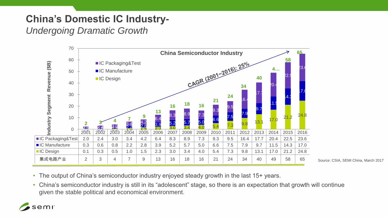
2001 2002 2003 2004 2005 2006 2007 2008 2009 2010 2011 2012 2013 2014 2015 2016
IC Packaging&Test 2.0 2.4 3.0 3.4 4.2 6.4 8.3 8.9 7.3 9.3 9.5 16.4 17.7 20.4 22.5 23.6
IC Manufacture 0.3 0.6 0.8 2.2 2.8 3.9 5.2 5.7 5.0 6.6 7.5 7.9 9.7 11.5 14.3 17.0
IC Design 0.1 0.3 0.5 1.0 1.5 2.3 3.0 3.4 4.0 5.4 7.3 9.8 13.1 17.0 21.2 24.8
集成电路产业 2 3 4 7 9 13 16 18 16 21 24 34 40 49 58 65
0.1 0.3 0.5 1.0 1.5 2.3 3.0 3.4 4.0 5.4 7.3 9.8 13.117.0
21.2 24.8
0.3 0.6 0.8 2.2 2.8 3.9 5.2 5.7 5.06.6
7.57.9
9.7
11.5
14.3
17.0
2.0 2.4 3.03.4 4.2
6.48.3 8.9 7.3
9.39.5
16.4
17.7
20.4
22.5
23.6
2 3 4 79
1316 18 16
2124
34
40
4…
58
65
0
10
20
30
40
50
60
70In
du
str
y S
eg
me
nt
Re
ve
nu
e (
$B
)China Semiconductor Industry
IC Packaging&Test
IC Manufacture
IC Design
China’s Domestic IC Industry-Undergoing Dramatic Growth
• The output of China’s semiconductor industry enjoyed steady growth in the last 15+ years.
• China’s semiconductor industry is still in its “adolescent” stage, so there is an expectation that growth will continue
given the stable political and economical environment.
Source: CSIA, SEMI China, March 2017

New Fab Projects on the Rise-
China leads the way
• 15 new fab projects in
China from 2017 on
• Majority of projects (10)
from China-owned entities

Surging China Fab InvestmentsWith Foundry & Memory leading
$U
SD
(M
illio
n)
Source: SEMI World Fab Forecast, June 2017
?
Key Spending Projects
2017• Intel Fab 68 - upgrade to 3D NAND
• SK Hynix C2
• UMC Fab 12X
• SMIC B2
2018• Intel Fab 68 Phase 2
• TSMC Nanjing Phase 1
• Hua Li Fab 2
• Fujian Jin Hua - DRAM
2019/2020• Tsinghua Unigroup (Nanjing) and Yangtze
Memory Technology (Wuhan)
• Samsung Xian phase 2
• SK Hynix C3
• GlobalFoundries Chengdu
• SMIC Beijing B3 and new Shanghai fab
• Hefei Chang Xin Memory

Leadframes
37%
SH Material(JPN)
Mitsui High-tec(JPN)
ASM Pacific (HK)
Shinko(JPN)
Kangqiang
Hualong
Trinity
Bonding Wire
32%
Heraeus(JPN)
Tanaka Denshi(JPN)
Nippon Micro (JPN)
Doublink
Kangqiang
Substrates
13%
Ibiden (JPN)
NanYa (TWN)
Shinko (JPN)
Samsung Electro-Mech. (KOR)
Shennan Circuits
Zhuhai Yueya
Encapsulation Resins
33%
Sumitomo Bakelite(JPN)
Henkel(GER)
Hitachi-Chemical (JPN))
Sinopaco
HHCK
Die attach Materials
23%
Henkel(GER)
Hitachi Chemical (JPN)
Sumitomo Bakelite (JPN)
Darbond
China Market
Share in 2016
Global
Companies
China
Mainland
Overview of Global Packaging Materials Suppliers in China
Source: SEMI China

Equipment & Materials
Market Forecast

2014 2015 2016 2017F 2018F
China 4.37 4.90 6.46 7.33 11.09
Europe 2.38 1.94 2.18 3.24 3.73
Japan 4.18 5.49 4.63 5.91 6.09
Korea 6.84 7.47 7.69 17.05 15.46
North America 8.16 5.12 4.49 5.10 5.71
SEA/ROW 2.15 1.97 3.55 2.87 3.17
Taiwan 9.41 9.64 12.23 12.83 10.93
$0
$10
$20
$30
$40
$50
$60
US
$ B
illio
ns
Taiwan SEA/ROW North America Korea Japan Europe China
$36.53$41.23
$54.33
$37.50
$56.18
SEMI® 2017 Equipment Forecast-
By Market Region
Source: SEMI September 2017New equipment. Totals may not add due to rounding
• Korea- record spending
year for any region
• Previous spending highs:• $12.9B N. America
(2000)
• $12.2B Taiwan (2016)

Semiconductor Fab Materials Markets
8+% Revenue Growth in 2017; 5+% Growth Forecasted for 2018
China8% Europe
10%
Japan18%
South Korea19%
North Americ
a17%
SEA/ROW5%
Taiwan23%
2016 = $24.7 billion
Region2017F
$US B
2018F
$US B
China $2.38 $2.68
Europe 2.70 2.78
Japan 4.50 4.60
South Korea 5.09 5.36
North America 4.60 4.80
SEA/ROW 1.40 1.49
Taiwan 6.23 6.59
Total $26.9 $28.3
Source: SEMI Materials Market Data Subscription, August 2017
Totals may not add due to rounding

Worldwide Wafer Fab Materials Forecast
Totals may not add due to roundingSource: SEMI August 2017
Actual Forecast
2015
US$ M
2016E
US$ M
2017
US$ M
2018
US$ M
Silicon Wafers1 $7,580 $7,650 $8,678 $9,086
Photomasks2 $3,267 $3,321 $3,462 $3,573
Photoresist $1,326 $1,450 $1,577 $1,662
Photoresist Ancillaries3 $1,796 $1,906 $2,051 $2,152
Wet Chemicals4 $1,416 $1,473 $1,531 $1,593
Gases $3,497 $3,631 $3,956 $4,152
Sputter Targets $628 $677 $707 $755
CMP Slurry & Pads5 $1,588 $1,667 $1,768 $1,835
Other/New Materials $2,853 $2,955 $3,122 $3,496
Total $23,952 $24,730 $26,853 $28,303
% Growth 3.2% 8.6% 5.4%

Semiconductor Packaging Materials Markets
China23%
Europe3%
Japan12%
South Korea13%
North Americ
a3%
SEA/ROW25%
Taiwan21%
2016 = $19.6 billion
Region2017F
$US B
2018F
$US B
China $4.65 $4.78
Europe 0.64 0.64
Japan 2.38 2.39
South Korea 2.48 2.49
North America 0.59 0.58
SEA/ROW 4.81 4.84
Taiwan 4.25 4.25
Total $19.8 $20.0
Source: SEMI Materials Market Data Subscription, August 2017
Totals may not add due to rounding

Worldwide Packaging Materials Forecast
Totals may not add due to rounding
Source: SEMI August 2017
Actual Forecast
2015
US$ M
2016E
US$ M
2017
US$ M
2018
US$ M
Leadframes $2,991 $3,038 $3,149 $3,190
Organic Substrates1 $7,779 $7,841 $7,658 $7,621
Ceramic Packages $2,082 $2,138 $2,206 $2,261
Encapsulation Resins $2,583 $2,758 $2,910 $2,987
Bonding Wire2 $2,966 $2,846 $2,809 $2,767
Die Attach Materials3 $679 $700 $749 $787
Others $258 $292 $323 $371
Total $19,338 $19,613 $19,804 $19,984
% Growth 1.4% 1.0% 1.0%

© 2017 TechSearch International, Inc.© 2017 TechSearch International, Inc.
Challenges for Large Area Panel Processing
• Economics to justify ROI– Large volume of a single part number with sufficiently large size– Not necessarily same applications as reconstituted wafer FO-WLP!!
• High accuracy placement is required, but high throughput is also needed
• Warpage (after mold and RDL) can cause tolerance issues, especially as feature size shrinks (≤10µm L/S)– Planarity issues (if die and mold are not planar, there will be line width distortion)– Warped panel makes die placement challenging and inspection difficult
• Dielectric dispense methods: dry film lamination? slot coating?
• Yield is critical– >98% are required for first RDL because compounding effect of yield can easily
diminish or eliminate savings in panel process– Mold compound is the largest source of defects (particles are generated during
thinning)– Final yield depends on quality of RDL

Summary

Summary
• 2017 will be a record setting year for the industry
– Record fab investments; All-time high for total equipment spending
– Spending in Korea will smash previous regional spending record
• Record spending forecasted for 2018
• China spending to surge in 2018 and could lead the market in 2019 & 2020
• Stronger revenue growth in fab materials compared to packaging materials
– Pricing recovery in silicon wafer market

Trends in the Materials Market in 2017
Mark Thirsk, Managing Partner, Linx Consulting

www.linx-consulting.com
Trends in the Materials Supply Ecosystem
• Mark Thirsk – Linx Consulting Inc.
SMC 2017

www.linx-consulting.com
Linx ESF
ESF 2017 Q3 Forecast
(August 2017)
2017Q1 2017Q2 2017Q3F 2017Q4F 2018Q1F 2018Q2F
MSI 2858 2978 3001 2875 2912 3183
%Change 3.4% 4.2% 0.8% -4.2% 1.3% 9.3%
%Change vs prior year 12.6% 10.1% 9.9% 4.0% 1.9% 6.9%
2,200
2,400
2,600
2,800
3,000
3,200
3,400
3,600
14 15 16 17 18 19
SEMIMSI
ESF 2017 Q3 (August)
ESF 2017 Q2 (May)
Annual Percent Change In MSI
2014 2015 2016 2017 2018 2019
11.4% 3.3% 2.9% 9.1% 7.1% 4.6%
Mill
ion
Sq
uar
e In
ches
History: Semi.org
Forecast: Hilltop Economics, LLC
SMC 2017

www.linx-consulting.com
Silicon Production Forecast
0
1000
2000
3000
4000
5000
6000
7000
2015 2016 2017 2018 2019 2020 2021
MSI by Device Type
Analog ASIC MPU DRAM NAND-2D NAND-3D
SMC 2017
Discretes not included
CAGR ‘16-’21
Analog 2.8%
ASIC 4.2%
MPU 0.4%
DRAM 6.7%
NAND-2D -22.8%
NAND-3D 58.9%

www.linx-consulting.com
300mm Annual Wafer Starts
-
10,000,000
20,000,000
30,000,000
40,000,000
50,000,000
60,000,000
2016 2017 2018 2019 2020 2021 2022 2023 2024 2025
ASIC MPU DRAM NAND-2D NAND-3D
SMC 2017

www.linx-consulting.com
≤200mm Annual Wafer Starts
-
5,000,000
10,000,000
15,000,000
20,000,000
25,000,000
30,000,000
2016 2017 2018 2019 2020 2021
Analog ASIC
SMC 2017Discretes not included
0
2,000,000
4,000,000
6,000,000
8,000,000
10,000,000
12,000,000
14,000,000
16,000,000
2016 2017 2018 2019 2020 2021 2022 2023 2024 2025
>= 350nm <350nm

www.linx-consulting.com
Technology trends
SMC 2017

www.linx-consulting.com
Technology Drivers
• Computing Demand
• Intelligent ubiquitous computing
• Multiple machine to machine networks for
• AI, Machine Learning, VR/AR and IOT
• Memory Bit growth
• Industry and Consumer demand increased demand to support computing growth
• Automotive
• Increase in automotive electronics
• ADAS
• Autonomous vehicles
• IOT
• Distributed sensors
• Edge cloud
• Cloud computing
• AR/VR
• Novel environments for improved performance
• Architecture change
• Scaling, equivalent scaling etc. are dead
• Silicon moving into the Third Dimension
• Process Needs
• Horizontal and vertical GAA Nanowires
• FET stacking
• Sub 10nm DRAM scaling
• Stackable storage class memory
• Dense MRAM
• Complex packaging
• 3D packaging for bit density improvement
• Hybrid FOWLP packaging
• CoWoS
• 3D x 3D Scaling
SMC 2017

www.linx-consulting.com
Device Trends
0
10
20
30
40
50
60
70
80
90
100
04 06 09 12 14 17 20 23 25
nm
Device Analysis
Logic
DRAM
2D NAND
3D NAND
Expon. (Logic)
Expon. (DRAM)
Expon. (2D NAND)
SMC 2017
Logic & DRAM - Min Metal 1/2 pitch (nm)2D NAND - Uncontacted poly 1/2 pitch (nm) 3D NAND Channel Hole (nm)
193i Single Patterning
193i LELE Patterning
193i SADP
193i SAQPEUV 2D SE
EUV 1D SE
EUV Multi-patterning
Source: IC Knowledge and Linx

www.linx-consulting.com
Automotive Growth
Impact Implication
Market $3 billion Processing market is anticipated to grow at 10+% CAGR, 2015 – 2020.
Growth still exist for 8 bit MCU as well as 32 and 64 bit devices for more complex applications.
Technology Trends
The level of processing power required for ECU consolidation will drive advanced designs.
Advanced devices will move to Foundry.
The level of processing power for “mainstream” body electronics will stay the same.
Growing demand for 8 bit MCU.
Quality Quality certification locks in processes and materials.
Significant barriers to entry and exit.
Complexity Safety and reliability drive redundancy.
Increased gate counts and complexity.
GreaterChina
Strong growth in auto production in China
Quality material supply will be required.
SMC 2017

www.linx-consulting.com
Storage Class Memory
3D SRAM
STT-MRAM
3D DRAM
STT-MRAM
FeRAM
eMRAM
3D NAND
3D XPoint
Co
st p
er
Bit
Pe
rfo
rma
nce
• Bit growth (AGR 2017):
• NAND ~45%
• DRAM ~15%
• DRAM lateral scaling is slowing and facing cost problems.
• There are no “universal” memory replacements, but new
segments are emerging.
Sources: AMAT, Micron
SMC 2017
-
1
2
3
4
$0
$100
$200
$300
$400
$500
2D NAND16nm
3D NAND 64L 3DXP 2L
Gb
/mm
2
NV Mem Material Cost
Wet strip chemicals
Wet etch chemicals
Wet clean chemicals
Spin-on
Reticles
Quartzware
PVD targets
Plating chemicals
Monitor wafers
Lithography materials
Implant sources
Dry etch gases
CVD precursors
CMP consumables
Bulk gases
Anneal gases
ALD
Bit Density Gb/mm2

www.linx-consulting.com
Materials Market Landscape
Analog 200mm
6%
Discrete 200mm
41%
ASIC 200mm
8%
ASIC6%
MPU3%
DRAM17%
NAND-2D13%
NAND-3D6%
2017 Si Demand - MSI
$-
$1.00
$2.00
$3.00
$4.00
$5.00
$6.00
$/sq in
SMC 2017

www.linx-consulting.com
Materials Markets
Analog 200mm
4%Discrete 200mm
12%
ASIC 200mm
7%
ASIC11%
MPU14%
DRAM25%
NAND-2D18%
NAND-3D9%
Materials Share by Device Type
ALD8% Anneal gases
1%
Bulk gases14%
CMP consumables
14%
CVD precursors
10%
Dry etch gases
6%
Implant sources
0%
Lithography materials
25%
Plating chemicals
1%
PVD targets4%
Spin-on10%
Wet clean chemicals
3%
Wet etch chemicals
3%
Wet strip chemicals
1%
Materials Segment
SMC 2017

www.linx-consulting.com
Film Deposition
• Demand Drivers
• CuBS demand increasing in Logic Interconnect
• Limitations of current architectures
• FinFET gate deposition
• GAA Nanowire development
• High mobility materials
• Memory technology extension
• 3D-NAND growth
• DRAM capacitor dielectric
• Novel architectures
• Pitch doubling and quadrupling
• Low temperature spacers
• Lithography aids
• Opportunities
• Possible changes in conductor metal
• Cu Co Barrier Ru?
• 3D-NAND aspect ratio
• Novel process development
• CVD Continuous etch
• ALD ALE
• Self Assembling Materials for selective processes
• Few new PVD applications
• 3DXpoint / MRAM?
• Complex supply chain requiring unique capabilities
• Supply of Co intermediates
SMC 2017

www.linx-consulting.com
CMP
Demand Drivers
• Continued addition of CMP processes
• CMP is becoming an enabling process
• Cleaning and particle removal through buff processes
• Implementation into SADP pattern transfer processes
• CMP of sacrificial layers for CDU
• Novel metals in MOL and BEOL processes
Opportunity
• High purity colloidal type abrasives are taking place in both silica and ceria segments for defect control.
• Close collaboration among CMP materials supply chain players is required to meet advanced CMP process requirements.
• Highly consolidated supply side.
• Integration of Polish and Cleaning processes to optimize defectivity.
• Local sources in China.
SMC 2017

www.linx-consulting.com
Patterning
Demand Drivers
• Increasing cost driver for advanced devices.
• Extension of resolution for 193i processes .
• Self aligned process patterning
• Mandrel thermal stability and cost
• SAQP MO spacers
• Multicolor cut mask processes
• High aspect ratio etch resistant hard masks.
• EUV implementation.
Opportunities
• Process aids
• Image reversal
• EPE improvement
• Photoresist smoothing strategies
• Etch
• Vapor
• DSA
• Deposition
EUV
• Source Power
• Acceptability of metal oxide nanoparticles
• Metal Oxide underlayers for EUV sensitivity
• Pellicle design
SMC 2017

www.linx-consulting.com
Worldwide Wafer Fab Materials Forecast
US$ Millions 2016 2017 2018 2020 CAGR
2016 to ‘20
ALD $311 $340 $456 $671 21%
CVD $1,292 $1,390 $1,565 $1,744 8%
PVD $728 $782 $817 $856 4%
Plating $185 $206 $225 $258 9%
Spin On Dielectrics $475 $512 $553 $525 3%
Pads and Slurries $1,908 $2,001 $2,090 $2,119 3%
Wet Chemicals $2,448 $2,597 $2,769 $2,960 5%
Lithography Materials $2,925 $3,081 $3,361 $3,553 5%
Etchant Gases $283 $301 $321 $368 7%
Dopant Gases $191 $165 $162 $172 -3%
Litho Gases $145 $159 $173 $208 9%
Total (Direct Mats) $10,891 $11,534 $12,492 $13,434 5%
SMC 2017

Application requirements driving the Technology Development
Marcel Wieland, Deputy Director Technology Development Globalfoundries

Holistic Approach 15–16 November 2017
Substrates
Materials
Components
Subassemblies
Equipment IP
Design
Fabless
Device
Manufacturing
Packaging
Test
System
Integration
Applications
R&D
Consortia
Potential topics along the value chain to be addressed in Call for Paper
• Automotive:
high reliability,
Grade 0-2
• E-vehicles
• Communication
RF: high
frequencies
about 300GHz
• Ultra low- k
material for
automotive
• Metrology
Focus FDSOI and Non Volatile Memory
• Over
molding
• Interposer
• Photonics
• WLP
• Antenna
integration
• Memory
integration
• Optic on
board (less
power
consumption)

Want to get more?
The Material Conference will focus on:
• Requirements for automotive (high reliability) and mobile communication (high frequency) applications
• FD-SOI and ferroelectric memories
Program
Session 1 - FDSOI - Continuation of Innovation
Session 2 - Microcontrollers and Nonvolatile Memories
Session 3 - Materials and Processes for Frontend/Backend of Line Applications
15–16 November 2017

Session 1 - FDSOI - Continuation of Innovation 15–16 November 2017

Session 1 - FDSOI - Continuation of Innovation 15–16 November 2017

Session 2 - Microcontrollers and Nonvolatile Memories
15–16 November 2017

Session 3 - Materials and Processes for Frontend/Backend of Line Applications
15–16 November 2017


Thank you!See you in Munich 14-17 NOV 2017