Computer System Architecture Dept. of Info. Of Computer Chap. 2 Digital Components 2-1 2-1...
15
Computer System Architecture Dept. of Info. Of Computer Chap. 2 Digital Components Chap. 2 Digital Components 2-1 2-1 Integrated Circuits Integrated Circuits(IC) Digital circuits are constructed with Integrated Circuits An Integrated Circuits is a small silicon semiconductor crystal, called chip The various gates are interconnected inside the chip to form the required circuit The chip is mounted in a ceramic or plastic container, and connections are welded by thin gold wires to external pins to form the integrated circuits The number of pins may range from 14 in a small IC package to 100 or more in a larger package Each IC has a numeric designation printed on the surface of the package for identification http://www.fullman.com/semiconductors/index.html Logic Family 에 에에 에에 MOSFET BJT MOS Family(N or P Channel) : High Component Density CMOS Family(N or P Channel) : Low Power TTL Family : 에에에에에 에에 에에 ECL Family : 에에에 에에에에 에에에에 에에 TTL 에 CMOS 에에에에
-
Upload
holly-jacobs -
Category
Documents
-
view
227 -
download
5
Transcript of Computer System Architecture Dept. of Info. Of Computer Chap. 2 Digital Components 2-1 2-1...

Computer System Architecture Dept. of Info. Of ComputerChap. 2 Digital ComponentsChap. 2 Digital Components
2-12-1 Integrated Circuits
Integrated Circuits(IC) Digital circuits are constructed with Integrated Circuits An Integrated Circuits is a small silicon semiconductor crystal, called chip The various gates are interconnected inside the chip to form the required
circuit The chip is mounted in a ceramic or plastic container, and connections are
welded by thin gold wires to external pins to form the integrated circuits The number of pins may range from 14 in a small IC package to 100 or
more in a larger package Each IC has a numeric designation printed on the surface of the package
for identification http://www.fullman.com/semiconductors/index.html Logic Family 에 의한 분류
MOSFET
BJT
MOS Family(N or P Channel) : High Component Density
CMOS Family(N or P Channel) : Low Power
TTL Family : 일반적으로 많이 사용
ECL Family : 고속을 요구하는 특수용도
현재 TTL 과 CMOS 주로사용

Computer System Architecture Dept. of Info. Of ComputerChap. 2 Digital ComponentsChap. 2 Digital Components
2-2
TTL Family 54 Series : -55 ° C 125 °C, Military
74 Series : 0 ° C 70 ° C, Commercial» 54/74 : Standard
» 54L/74L : Low-power
» 54S/74S : Schottky
» 54LS/74LS : Low-power, Schottky
» 54H/74H : High-speed
CMOS Family 4000 Series(RCA), MC14500(Motorola), 5000(Toshiba), 54C/74C Series,
54HC/74HC Series» 동작온도 : -30 ° C 85 ° C , Fan-out 증가 , Noise Margin 증가 , Low-power
* Schottky Diode금속과 반도체를 연결하면 ECL 보다는 느리지만 동작속도가 빨라짐( 0.4 Volt 에서 동작 )
Pt Si
0.2 0.4 0.6V
i
Schottky Diode Schottky Transistor Forward Bias

Computer System Architecture Dept. of Info. Of ComputerChap. 2 Digital ComponentsChap. 2 Digital Components
2-3Package Types
Small Outline Transistor (SOT) Small Outline Package (SOP) Dual-In-Line Package (DIP)
Plastic/Ceramic Pin Grid Array (PPGA/CPGA)
Plastic Leaded Chip Carrier (PLCC)

Computer System Architecture Dept. of Info. Of ComputerChap. 2 Digital ComponentsChap. 2 Digital Components
2-4
Plastic Quad Flat Package (PQFP)
TO Packages (Transistor single Outline)
Ceramic Leadless Chip Carrier (LCC)
Computer System Architecture Dept. of Info. Of ComputerChap. 2 Digital ComponentsChap. 2 Digital Components
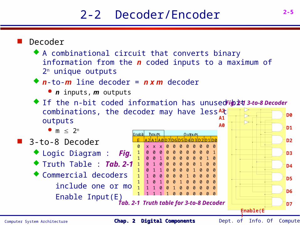
2-52-2 Decoder/Encoder
Decoder A combinational circuit that converts binary information from the n
coded inputs to a maximum of 2n unique outputs n-to-m line decoder = n x m decoder
n inputs, m outputs
If the n-bit coded information has unused bit combinations, the decoder may have less than 2n outputs
m 2n
3-to-8 Decoder Logic Diagram : Fig. 2-1 Truth Table : Tab. 2-1 Commercial decoders
include one or more
Enable Input(E)
Fig. 2-1 3-to-8 Decoder
Tab. 2-1 Truth table for 3-to-8 Decoder
A2
A1
A0
D0
D1
D2
D3
D4
D5
D6
D7Enable(E)
Enable
E A2 A1 A0 D7 D6 D5 D4 D3 D2 D1 D00 x x x 0 0 0 0 0 0 0 01 0 0 0 0 0 0 0 0 0 0 11 0 0 1 0 0 0 0 0 0 1 01 0 1 0 0 0 0 0 0 1 0 01 0 1 1 0 0 0 0 1 0 0 01 1 0 0 0 0 0 1 0 0 0 01 1 0 1 0 0 1 0 0 0 0 01 1 1 0 0 1 0 0 0 0 0 01 1 1 1 1 0 0 0 0 0 0 0
Inputs Outputs

Computer System Architecture Dept. of Info. Of ComputerChap. 2 Digital ComponentsChap. 2 Digital Components
2-6
NAND Gate Decoder Constructed with NAND instead of AND gates Logic Diagram/Truth Table : Fig. 2-2
Decoder Expansion 3 X 8 Decoder constructed with two 2 X 4 Decoder Constructed decoder : Fig. 2-3
Encoder Inverse Operation of a decoder 2n input, n output Truth Table : Tab. 2-2
3 OR Gates Implementation» A0 = D1 + D3 + D5 + D7
» A1 = D2 + D3 + D6 + D7
» A2 = D4 + D5 + D6 + D7
* Active Low Output* Fig. 2-1 3-to-8 Decoder 는 Active High Output
Enable
E A1 A0 D3 D2 D1 D00 x x 0 0 0 01 0 0 0 0 0 11 0 1 0 0 1 01 1 0 0 1 0 01 1 1 1 0 0 0
Input OutputA0
A1
D0
D1
D2
D3Enable(E)
a11
a22
3a3
b1
b2
b3
b4
5
6
7
8
2 X 4Decoder
20
21
E
a11
a22
3a3
b1
b2
b3
b4
5
6
7
8
2 X 4Decoder
20
21
E
A2
A1
A0
D0D1D2D3
D4D5D6D7
D7 D6 D5 D4 D3 D2 D1 D0 A2 A1A00 0 0 0 0 0 0 1 0 0 00 0 0 0 0 0 1 0 0 0 10 0 0 0 0 1 0 0 0 1 00 0 0 0 1 0 0 0 0 1 10 0 0 1 0 0 0 0 1 0 00 0 1 0 0 0 0 0 1 0 10 1 0 0 0 0 0 0 1 1 01 0 0 0 0 0 0 0 1 1 1
OutputsInputs
Fig. 2-2 2-to-4 Decoder with NAND gates
(a) Truth Table
(b) Logic Diagram
Fig. 2-3 A 3-to-8 Decoder constructed with two with 2-to-4 Decoder
Tab. 2-2 Truth Table for Encoder

Computer System Architecture Dept. of Info. Of ComputerChap. 2 Digital ComponentsChap. 2 Digital Components
2-72-3 Multiplexers
Multiplexer(Mux) A combinational circuit that receives binary information from one of 2n input data lines and directs it to a
single output line A 2n -to 1 multiplexer has 2n input data lines and
n input selection lines(Data Selector) 4-to-1 multiplexer Diagram : Fig. 2-4 4-to-1 multiplexer Function Table : Tab. 2-3
Quadruple 2-to-1 Multiplexer Quadruple 2-to-1 Multiplexer : Fig. 2-5
Select OutputS1 S0 Y 0 0 I0 0 1 I1 1 0 I2 1 1 I3
I0
I1
I2
I3
S0S1
Y
Tab. 2-3 Function Table for 4-to-1 line Multiplexter
Fig. 2-4 4-to-1 Line Multiplexer
Select OutputE S Y 0 0 All 0's 1 0 A 1 1 B
Quadruple 2 x 1 Mux
A0
A1
A2
A3B0
B1
B2
B3
Y0
Y1
Y2
Y3
EnableSelect
Fig. 2-5 Quadruple 2-to-1 line Multiplexter
(a) Function Table (b) Block Diagram

Computer System Architecture Dept. of Info. Of ComputerChap. 2 Digital ComponentsChap. 2 Digital Components
2-82-4 Registers
Register A group of flip-flops with each flip-flop capable of storing one bit of
information An n-bit register has a group of n flip-flops and is capable of storing any
binary information of n bits The simplest register consists only of flip-flops, with no external gate :
Fig. 2-6 A clock input C will load all four inputs in parallel
The clock must be inhibited if the content of the register must be left unchanged
Register with Parallel Load A 4-bit register with a load control input : Fig. 2-7 The clock inputs receive clock pulses at all times The buffer gate in the clock input will increase “fan-out” Load Input
1 : Four input transfer 0 : Input inhibited, Feedback from output to input(no change)
Q
QSET
C LR
D
Q
QSET
C LR
D
Q
QSET
C LR
D
Q
QSET
C LR
D
I0
I1
I2
I3
Clock
Clear
A0
A1
A2
A3
Fig. 2-6 4-bit register

Computer System Architecture Dept. of Info. Of ComputerChap. 2 Digital ComponentsChap. 2 Digital Components
2-92-5 Shift Registers
Shift Register A register capable of shifting its binary
information in one or both directions The logical configuration of a shift register
consists of a chain of flip-flops in cascade The simplest possible shift register uses
only flip-flops : Fig. 2-8 The serial input determines what goes
into the leftmost position during the shift The serial output is taken from the
output of the rightmost flip-flop
Q
Q
D
Q
Q
D
Q
Q
D
Q
Q
D
Fig. 2-7 4-bit register with parallel loadFig. 2-8 4-bit shift register

Computer System Architecture Dept. of Info. Of ComputerChap. 2 Digital ComponentsChap. 2 Digital Components
2-10
Bidirectional Shift Register with Parallel Load A register capable of shifting in one direction only is called a
unidirectional shift register A register that can shift in both directions is called a bidirectional shift
register The most general shift register has all the
capabilities listed below: An input clock pulse to synchronize all operations A shift-right /left (serial output/input) A parallel load, n parallel output lines The register unchanged even though clock pulses
are applied continuously
4-bit bidirectional shift register with parallel load : Fig. 2-9
4 X 1 Mux = 4 개 , D F/F = 4 개 Mode Operation
S1 S0 0 0 No chage 0 1 Shift right(down) 1 0 shift left(up) 1 1 Parallel load
Tab. 2-4 Function Table for Register of Fig. 2-9 Fig. 2-9 Bidirectional shift register

Computer System Architecture Dept. of Info. Of ComputerChap. 2 Digital ComponentsChap. 2 Digital Components
2-112-6 Binary Counter
Counter A register goes through a predetermined sequence of state(Upon the
application of input pulses) Used for counting the number of occurrences of an event and useful for
generating timing signals to control the sequence of operations in digital computers
An n-bit binary counter is a register of n flip-flop(count from 0 to 2n -1) 4 bit Synchronous Binary Counter
A counter circuit will usually employ F/F with complementing capabilities(T and J-K F/F)
4 bit Synchronous Binary Counter :
Fig. 2-10
J K0 01 1 Q(t)'
Q(t+1)Q(t)
Fig. 2-10 4-bit Synchronous binary counter
J
Q
Q
K
J
Q
Q
K
J
Q
Q
K
J
Q
Q
K
Count Enable
Clock
Carry = Q3• Q2’
Q0 Q0’ Q1 Q1’ Q2 Q2’ Q3

Computer System Architecture Dept. of Info. Of ComputerChap. 2 Digital ComponentsChap. 2 Digital Components
2-12
Binary Counter with Parallel Load Counters employed in digital
systems(CPU Register) require a parallel load capability for transferring an initial binary number prior to the count operation
4-bit binary counter with Clear, Parallel Load, and Increment(Counter) :
Fig. 2-11 Function Table : Tab. 2-5
Clear : 1 K=X, J=0 Clear(Q=0)
(Clear, Load=X)
Load : 1 I=1 J=1, K=0
(Clear=0) I=0 J=0, K=1
Increment : 1 J=K=1(Toggle)
(Clear, Load=0)
J K0 00 11 01 1 Q(t)'
Q(t+1) Q(t)
01
J
Q
Q
K
J
Q
Q
K
J
Q
Q
K
J
Q
Q
K
Fig. 2-11 4-bit binary counter with parallel load

Computer System Architecture Dept. of Info. Of ComputerChap. 2 Digital ComponentsChap. 2 Digital Components
2-132-7 Memory Unit
Memory Unit A collection of storage cells together with associated circuits needed to
transfer information in and out of storage The memory stores binary information in groups of bits called words Word
A group of binary information that is processed in one simultaneous operation
Byte A group of eight bits (nibble : four bits)
The number of address line = k Address(Identification number) : 0, 1, 2, 3, … up to 2k -1 The selection of specific word inside memory : k bit binary address 1 Kilo= 210, 1 Mega= 220, 1 Giga= 230
16 bit address line 예제 : 216= 64 K
Solid State Memory(IC Memory) RAM(Volatile Memory) ROM(Non-volatile Memory)
MemoryWord
Dec Hex 0 0000 1 0001 2 0010 3 0011 . . . . . . 65535 FFFF

Computer System Architecture Dept. of Info. Of ComputerChap. 2 Digital ComponentsChap. 2 Digital Components
2-14
Random Access Memory The memory cells can be accessed for information transfer from any
desired random location Communication between a memory and its environment is achieved
through data input and output lines, address selection lines, and control lines : Fig. 2-12
The two operations that a random-access memory can perform are the write and read operations
Memory Write1) Apply the binary address
2) Apply the data bits
3) Activate the write input
Memory Read1) Apply the binary address
2) Activate the read input» The content of the selected word does
not change after reading
NV-RAM : battery back-up CMOS RAMFig. 2-12 Block diagram of RAM
Memory Unit 2k words
n bits per word
data input lines n
data output lines n
address lines k Read Write

Computer System Architecture Dept. of Info. Of ComputerChap. 2 Digital ComponentsChap. 2 Digital Components
2-15
Read-Only Memory A memory unit that performs the read operation only; it does not have a
write capability ROM comes with special internal electronic fuses that can be
“programmed” for a specific configuration m x n ROM : Fig. 2-13
k address input lines to select one of 2k = m words of memory, and n output lines(n bits word)
ROM is classified as a combinational circuit, because the outputs are a function of only the present inputs(address lines)
There is no need for providing storage capabilities as in a RAM
ROM is also employed in the design of control units for digital computers
A Control Unit that utilizes a ROM to store binary control information is called a micro-programmed control
Types of ROMs UVEPROM(Chip level erase), EEPROM(Byte level erase), Flash ROM(Page
or block level erase), OTPROM, Mask ROM
m x n ROM (m = 2k)
address input lines k
data input lines n