Complexity Reduction in the CORDIC Algorithm by using...
52
1 Complexity Reduction in the CORDIC Algorithm by using MUXes By Yuhang Sun Department of Electrical and Information Technology Faculty of Engineering, LTH, Lund University SE-221 00 Lund, Sweden
Transcript of Complexity Reduction in the CORDIC Algorithm by using...
1
Complexity Reduction in the
CORDIC Algorithm by using
MUXes
By
Yuhang Sun
Department of Electrical and Information Technology
Faculty of Engineering, LTH, Lund University
SE-221 00 Lund, Sweden

2

3
Abstract
Nowadays, the CORDIC algorithm plays an important role to deal with
the non-linear functions in hardware. In this thesis, a novel methodology is
described to reduce the complexity in an unrolled CORDIC architecture,
which gives higher speed, lesser area, and lower power consumption. That
is, MUXes are used to replace adder stages. Five different unrolled
CORDIC architectures have been implemented in ASIC using a 65nm
CMOS technology with Low Power High 𝑉𝑇 transistors. The area,
computational speed, accuracy, error behavior, and power consumption
have been analyzed. The design aim is to reduce the power consumption,
which is more and more important depending on the area. As a result the
area and power consumption get 7.9% lower and 27.2% lower separately,
and the speed is 22.9% higher compared to the original unrolled CORDIC
architecture.
Keywords: CORDIC, power consumption.
4
Acknowledgments
This Master’s thesis would not exist without the support and guidance
of many people, my friends, my parents, especially my supervisors.
I would like to express my deepest gratitude to my supervisors,
Professor Peter Nilsson, Erik Hertz, and Rakesh Gangarajaiah who guided
me and helped me in this thesis work.
Finally, thanks to my relatives who kept encouraging me and my
parents who afford me to study in Sweden
Yuhang Sun
5
Contents Abstract ......................................................................................................... 3
Acknowledgments ......................................................................................... 4
List of figures ................................................................................................. 7
List of tables .................................................................................................. 8
List of acronyms .......................................................................................... 10
1. Introduction ......................................................................................... 11
Thesis outlines ............................................................................. 12 1.1.
2. Theory .................................................................................................. 13
The CORDIC algorithm ................................................................. 13 2.1.
Two starting angles ..................................................................... 16 2.2.
Four starting angles ..................................................................... 17 2.3.
3. Software simulation ............................................................................ 21
Outputs simulation ...................................................................... 21 3.1.
Error behavior ............................................................................. 22 3.2.
Accuracy ...................................................................................... 24 3.3.
4. Hardware implementation .................................................................. 25
Design flow .................................................................................. 25 4.1.
Hardware architectures and simulation results .......................... 26 4.2.
4.2.1. The original unrolled CORDIC architecture ......................... 26
4.2.2. First stage removed architecture ........................................ 28
4.2.3. Two stages eliminated architecture .................................... 30
4.2.4. Three stages eliminated architecture ................................. 31
4.2.5. Final architecture ................................................................. 33
5. Results ................................................................................................. 37
Test setup .................................................................................... 37 5.1.

6
The area ....................................................................................... 37 5.2.
Timing information ...................................................................... 39 5.3.
Power consumption .................................................................... 40 5.4.
5.4.1. Power analysis ..................................................................... 40
6. Conclusions .......................................................................................... 45
7. Future work ......................................................................................... 47
References ................................................................................................... 49
Appendix A .................................................................................................. 51
7
List of figures
Fig. 1. Vector rotations diagram (five stages) ................................ 14 Fig. 2. The last vector ends up on the unit circle (five stages) ...... 15
Fig. 3. Two starting angles (three stages) ...................................... 16 Fig. 4. Four starting angles (two stages) ........................................ 18 Fig. 5. MATLAB simulation of CORDIC design.......................... 21
Fig. 6. The cosine error after truncation ........................................ 22 Fig. 7. The cosine error distribution............................................... 23
Fig. 8. The absolute cosine error in dB .......................................... 23 Fig. 9. Degrees and the number of error bits ................................. 24 Fig. 10. The design flow ............................................................... 25
Fig. 11. An unrolled 5-stage CORDIC architecture ..................... 26
Fig. 12. First stage removed architecture ..................................... 28 Fig. 13. Two stages are removed in the architecture .................... 30 Fig. 14. Three stages are removed architecture ............................ 32
Fig. 15. Final architecture ............................................................ 33 Fig. 16. The Sgn detector ............................................................. 34
Fig. 17. The design test setup ....................................................... 37 Fig. 18. Area at different frequencies ........................................... 38 Fig. 19. Power at various frequencies .......................................... 42
Fig. 20. magnified diagram for Fig. 19 ........................................ 43
8
List of tables
Power at 10MHz .......................................................... 27 TABLE I.
Power at maximum frequency ..................................... 27 TABLE II.
Timing at maximum speed constraints .................... 27 TABLE III.
Timing at minimum area constraints ....................... 27 TABLE IV.
Area at minimum area constraints .............................. 28 TABLE V.
Area at maximum speed constraints ........................ 28 TABLE VI.
Power at 10MHz ...................................................... 29 TABLE VII.
Power at maximum frequency ................................. 29 TABLE VIII.
Timing at maximum speed constraints .................... 29 TABLE IX.
Timing at minimum area constraints ........................... 29 TABLE X.
Area at minimum area constraints .......................... 29 TABLE XI.
Area at maximum speed constraints ........................ 29 TABLE XII.
Power at 10MHz ...................................................... 30 TABLE XIII.
Power at maximum frequency ............................. 31 TABLE XIV.
Timing at maximum speed constraints .................... 31 TABLE XV.
Timing at minimum area constraints ................... 31 TABLE XVI.
Area at minimum area constraints ...................... 31 TABLE XVII.
Area at maximum speed constraints .................... 31 TABLE XVIII.
Power at 10MHz .................................................. 32 TABLE XIX.
Power at maximum frequency ................................. 32 TABLE XX.
Timing at maximum speed constraints ................ 32 TABLE XXI.
Timing at minimum area constraints ................... 33 TABLE XXII.
Area at minimum area constraints ...................... 33 TABLE XXIII.
Area at maximum speed constraints .................... 33 TABLE XXIV.
Power at 10MHz .................................................. 34 TABLE XXV.
Power at maximum frequency ............................. 34 TABLE XXVI.
Timing at maximum speed constraints ................ 35 TABLE XXVII.
Timing at minimum area constraints ................. 35 TABLE XXVIII.
Area at minimum area constraints ...................... 35 TABLE XXIX.
Area at maximum speed constraints .................... 35 TABLE XXX.
Area at minimum area constraints ....................... 38 TABLE XXXI.

9
Area at maximum speed constraints .................... 39 TABLE XXXII.
Timing at maximum speed constraints .............. 39 TABLE XXXIII.
Timing at minimum area constraints ................. 40 TABLE XXXIV.
Power at maximum speed constraints ................. 41 TABLE XXXV.
Power at minimum area constraints ................... 42 TABLE XXXVI.
Coefficient angles ............................................. 51 TABLE XXXVII.

10
List of acronyms
CORDIC COordinated Rotation DIgital Computer
LUT Look Up Table
ASIC Application Specific Integrated Circuit
VHDL Very High speed integrated circuit Hardware
Description Language
CMOS Complementary Metal Oxide Semiconductor
VCD Value Change Dump
VLSI Very Large Scale Integrated circuit

11
1. Introduction
In most cases, non-linear functions play an important role in hardware.
The area, computational speed, accuracy, error behavior, and the power
consumption are the important factors that we need to consider in the
hardware design. There are several algorithms that can be chosen for
implementation of non-linear functions.
Look-Up Table (LUT) is a simple and direct method to compute non-
linear functions. However, a look-up table is suitable if the precision is low
or the area is not necessarily considered. The size of the table grows
exponentially, which makes this method unsuitable for hardware design
when the precision goes high.
Another method, Parabolic Synthesis [1] is used to compute unary
functions with parabolic functions. It is a novel methodology that came up
with a high speed computational technology. The advantage of this method
is that the delay is short.
Polynomial approximations [2] are implemented with multipliers and
adders, using an iterative algorithm. Which polynomial curves we choose
leads to how closely the polynomial curve can follow the special function.
That is where the error is generated. Very high order polynomials are used if
high accuracy is required. To meet the requirement, the polynomial
approximations can be implemented with least squares approximations,
which minimize the average error, or least maximum approximations, which
minimize the worst-case error.
This thesis work is focus on the CORDIC algorithm. The CORDIC
algorithm is an efficient algorithm to compute non-linear functions in
hardware.
The COordinate Rotation Digital Computer (CORDIC) algorithm [3],
also known as the digit-by-digit method or the Volder’s algorithm, was first
described by Jack E. Volder in 1959. It is an efficient algorithm to compute
non-linear functions especially trigonometric functions in hardware design.
Compared to other methods described above, the CORIDC has no
multipliers, which means that it is only based on additions, subtractions and
bit shifts. Traditionally, iterative CORDICs [4] have been widely used since
the cost of area is less.
Nowadays, power consumption is more important than the area
parameter, [5] in hardware design, which leads to that unrolled CORDICs
are feasible to use. Meanwhile, it is necessary to reduce the complexity
12
since it can also reduce the power consumption, which is the aim of this
thesis.
The implementation includes five different unrolled CORDIC
architectures in an Application Specific Integrated Circuit (ASIC). One is
the original CORDIC architecture and the other four are CORDIC
architectures, with reduced complexities on various levels. The designs are
written in Very High Speed Integrated Circuit Hardware Description
Language (VHDL) using a 65nm CMOS technology with Low Power High
𝑉𝑇 transistors. The used supply voltage is VDD = 1.2 volts and the
temperature is 25 degrees.
As a result, area, timing, and power consumption, operating under
different frequencies, are reported for the five different unrolled CORDIC
architectures.
Thesis outlines 1.1.
Remaining sections are outlined below:
Section 2 introduces the CORIDC algorithm and methods to reduce the
complexity.
Section 3 describes the software simulation, accuracy, and error
behavior of the CORIDC algorithm.
Section 4 describes the hardware implementations of the five different
unrolled CORIDC architectures.
Section 5 lists and analyzes the result of section 4, consisting of area,
timing and power consumption.
Section 6 concludes this thesis work.
Section 7 analyzes possible future work after this thesis work.
13
2. Theory
In this section, the CORDIC algorithm and the methods to reduce the
complexities are introduced. Using two starting angles and four starting
angles together with MUXes will reduce one adder stage and two adder
stages separately in the unrolled CORDIC architectures.
The CORDIC algorithm 2.1.
The CORDIC algorithm, based on vector rotations is used to get an
approximation of the non-linear function. In this thesis, the sine functions
and cosine functions are the functions that are implemented with the
CORDIC algorithm. An iterative CORDIC architecture consists of several
adder stages. When the numbers of stages increased, the error between the
approximation and the original function gets smaller, which leads to an
improved accuracy.
In Fig. 1, a 30 degree angle is taken to be the input angle. There are five
vector rotations, which mean there are five stages. The initial vector, a 0
degree angle, is rotated by 45 degrees, which is detected to be larger than
the input angle. In next stage, the vector is rotated -27 degrees and so on, to
approximate the input angle. The positive degrees means the direction of the
rotation is counter clockwise, the negative degrees means the direction of
the rotation is clockwise. After five vector rotations, the last vector’s angle
approximates the input angle.
To improve the accuracy, more stages can be used. This will make the
approximation infinitely close to the input angle. The angles 45 and 27
degrees are the coefficient angles, which are shown in Table XXXIII in
Appendix A.

14
Fig. 1. Vector rotations diagram (five stages)
The function of coefficient angles is shown in (1). Where 𝑎𝑛𝑔𝑙𝑒(𝑖) is
the coefficient angle, 𝑖 is the number of stages. The first five coefficient
angles are given in (2).
𝑎𝑔𝑛𝑙𝑒(𝑖) = 𝑎𝑟𝑐𝑡𝑎𝑛(1 2𝑖−1⁄ ) (1)
{
𝑎𝑛𝑔𝑙𝑒(1) = 𝑎𝑟𝑐𝑡𝑎𝑛(1 21−1⁄ ) = 45
𝑎𝑛𝑔𝑙𝑒(2) = 𝑎𝑟𝑐𝑡𝑎𝑛(1 22−1⁄ ) = 26.56
𝑎𝑛𝑔𝑙𝑒(3) = 𝑎𝑟𝑐𝑡𝑎𝑛(1 23−1⁄ ) = 14.04
𝑎𝑛𝑔𝑙𝑒(4) = 𝑎𝑟𝑐𝑡𝑎𝑛(1 24−1⁄ ) = 7.13
𝑎𝑛𝑔𝑙𝑒(5) = 𝑎𝑟𝑐𝑡𝑎𝑛(1 25−1⁄ ) = 3.58
(2)
The output is the last vector coordinates, (𝑥, 𝑦). In this paper, CORDIC
algorithm is used to deal with the sine function and cosine function. The
approximated sine and cosine value of the input angle are shown in (3) and
(4).
sin𝑎 =𝑦
𝑟
(3)
cos 𝑎 =𝑥
𝑟
(4)
15
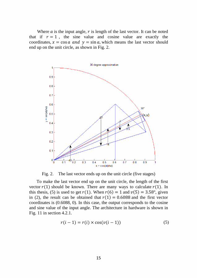
Where 𝑎 is the input angle, 𝑟 is length of the last vector. It can be noted
that if 𝑟 = 1 , the sine value and cosine value are exactly the
coordinates, 𝑥 = cos𝑎 𝑎𝑛𝑑 𝑦 = sin 𝑎, which means the last vector should
end up on the unit circle, as shown in Fig. 2.
Fig. 2. The last vector ends up on the unit circle (five stages)
To make the last vector end up on the unit circle, the length of the first
vector 𝑟(1) should be known. There are many ways to calculate 𝑟(1). In
this thesis, (5) is used to get 𝑟(1). When 𝑟(6) = 1 and 𝑣(5) = 3.58°, given
in (2), the result can be obtained that 𝑟(1) = 0.6088 and the first vector
coordinates is (0.6088, 0). In this case, the output corresponds to the cosine
and sine value of the input angle. The architecture in hardware is shown in
Fig. 11 in section 4.2.1.
𝑟(𝑖 − 1) = 𝑟(𝑖) × cos(𝑣(𝑖 − 1)) (5)
16
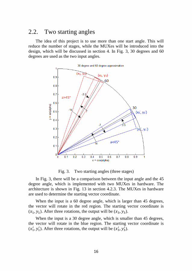
Two starting angles 2.2.
The idea of this project is to use more than one start angle. This will
reduce the number of stages, while the MUXes will be introduced into the
design, which will be discussed in section 4. In Fig. 3, 30 degrees and 60
degrees are used as the two input angles.
Fig. 3. Two starting angles (three stages)
In Fig. 3, there will be a comparison between the input angle and the 45
degree angle, which is implemented with two MUXes in hardware. The
architecture is shown in Fig. 13 in section 4.2.3. The MUXes in hardware
are used to determine the starting vector coordinate.
When the input is a 60 degree angle, which is larger than 45 degrees,
the vector will rotate in the red region. The starting vector coordinate is
(𝑥1, 𝑦1). After three rotations, the output will be (𝑥3, 𝑦3).
When the input is a 30 degree angle, which is smaller than 45 degrees,
the vector will rotate in the blue region. The starting vector coordinate is
(𝑥1′ , 𝑦1
′). After three rotations, the output will be (𝑥3′ , 𝑦3
′ ).
17
When the input angle is exactly 45 degrees, both red lines and blue lines
are suitable for the vector rotations.
𝑣(1) = {𝑎𝑟𝑐𝑡𝑎𝑛(1) − 𝑎𝑟𝑐𝑡𝑎𝑛(1 2⁄ ) = 18.43𝑎𝑟𝑐𝑡𝑎𝑛(1) + 𝑎𝑟𝑐𝑡𝑎𝑛(1 2⁄ ) = 71.56
(6)
Equation (6) indicates that, the starting vector angles are 18.4349
degrees for the input angle below 45 degrees and 71.5651 degrees for angles
above 45 degrees. Fig. 11 in section 4.2.1 shows the original unrolled
CORDIC architecture, where the starting vector’s coordinates for Fig. 3 can
be obtained.
From the left of the architecture in Fig. 11, the first stage, is shown in
(7), where 𝑥1 is the 𝑟(1) in section 2.1.
{𝑦2 = 𝑥1𝑥2 = 𝑥1
(7)
{𝑦3 = 𝑦2 +
𝑥22=3𝑥12= 0.9132
𝑥3 = 𝑥2 −𝑦22=𝑥12= 0.3044
(8)
{𝑦3 = 𝑦2 −
𝑥22=𝑥12= 0.3044
𝑥3 = 𝑥2 +𝑦22=3𝑥12= 0.9132
(9)
In the second stage, the starting vector coordinates can be obtained.
When the input is larger than 45 degrees, the coordinates shown in (8) will
be used and when lesser than 45 degrees, the coordinate shown in (9) will
be used. This will make the architecture in Fig. 13 has two stages lesser than
the one in Fig. 11.
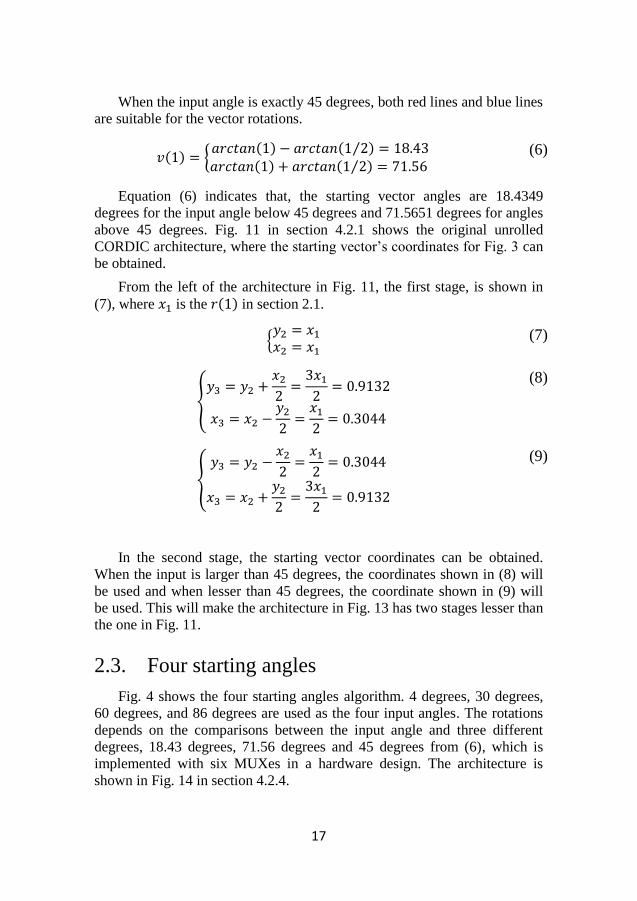
Four starting angles 2.3.
Fig. 4 shows the four starting angles algorithm. 4 degrees, 30 degrees,
60 degrees, and 86 degrees are used as the four input angles. The rotations
depends on the comparisons between the input angle and three different
degrees, 18.43 degrees, 71.56 degrees and 45 degrees from (6), which is
implemented with six MUXes in a hardware design. The architecture is
shown in Fig. 14 in section 4.2.4.
18
Fig. 4. Four starting angles (two stages)
𝑣(1) = {
𝑎𝑟𝑐𝑡𝑎𝑛(1) − 𝑎𝑟𝑐𝑡𝑎𝑛(1 2⁄ ) − 𝑎𝑟𝑐𝑡𝑎𝑛(1 4⁄ ) = 4.40𝑎𝑟𝑐𝑡𝑎𝑛(1) − 𝑎𝑟𝑐𝑡𝑎𝑛(1 2⁄ ) + 𝑎𝑟𝑐𝑡𝑎𝑛(1 4⁄ ) = 32.47𝑎𝑟𝑐𝑡𝑎𝑛(1) + 𝑎𝑟𝑐𝑡𝑎𝑛(1 2⁄ ) − 𝑎𝑟𝑐𝑡𝑎𝑛(1 4⁄ ) = 57.53𝑎𝑟𝑐𝑡𝑎𝑛(1) + 𝑎𝑟𝑐𝑡𝑎𝑛(1 2⁄ ) + 𝑎𝑟𝑐𝑡𝑎𝑛(1 4⁄ ) = 85.60
(10)
Equation (10) indicates the starting vector angles for the input angles in
four different regions. When the input angle is from 0 degree to 18.43
degrees, the starting vector angle is 4.40 degrees. When the input angle is
from 18.43 degrees to 45 degrees, the starting vector angle is 32.47 degrees.
When the input angle is from 45 degrees to 71.56 degrees, the starting
vector angle is 57.53 degrees. When the input angle is from 71.56 degrees to
90 degrees, the starting vector angle is 85.60 degrees.
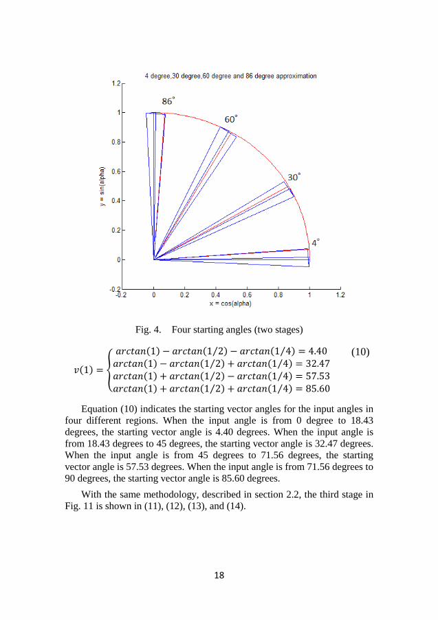
With the same methodology, described in section 2.2, the third stage in
Fig. 11 is shown in (11), (12), (13), and (14).
19
{𝑦4 = 𝑦3 −
𝑥34=𝑥12−3𝑥18=𝑥18= 0.0761
𝑥4 = 𝑥3 +𝑦34=3𝑥12+𝑥18=13𝑥18
= 0.9893
(11)
{𝑦4 = 𝑦3 +
𝑥34=𝑥12+3𝑥18=7𝑥18= 0.5327
𝑥4 = 𝑥3 −𝑦34=3𝑥12−𝑥18=11𝑥18
= 0.8371
(12)
{𝑦4 = 𝑦3 −
𝑥34=3𝑥12−𝑥18=11𝑥18
= 0.8371
𝑥4 = 𝑥3 +𝑦34=𝑥12+3𝑥18=7𝑥18= 0.5327
(13)
{𝑦4 = 𝑦3 +
𝑥34=3𝑥12+𝑥18=13𝑥18
= 0.9893
𝑥4 = 𝑥3 −𝑦34=𝑥12−3𝑥18=𝑥18= 0.0761
(14)
When the input angle is from 0 degree to 18.43 degrees, the coordinate
shown in (11) will be used. When the input angle is from 18.43 degrees to
45 degrees, the coordinate shown in (12) will be used. When the input angle
is from 45 degrees to 71.56 degrees, the coordinate shown in (13) will be
used. When the input angle is from 71.56 degrees to 90 degrees, the
coordinate shown in (14) will be used. This will make the architecture in Fig.
14 has three stages lesser than the one in Fig. 11.

20

21
3. Software simulation
In this section, the outputs of the designs are simulated in
MATLAB. The error behavior and accuracy tests are done in this
section as well.
Outputs simulation 3.1.
In this section, the original CORDIC architecture, shown in Fig. 11, is
simulated in MATLAB. The outputs of the sine and cosine functions are
shown in Fig. 5. To improve the accuracy, 18 stages are used. Note that all
architectures are simulated with the same result.
Fig. 5. MATLAB simulation of CORDIC design
Fig. 5 shows the approximated cosine outputs, theoretical cosine
outputs, approximated sine outputs, and theoretical sine outputs with
various input degrees. The green line and the black line, the blue line and
the red line match each other. That is, the simulated CORIDC functions
approximate the theoretical (floating point) functions, which is acceptable.
0 10 20 30 40 50 60 70 80 90-0.2
0
0.2
0.4
0.6
0.8
1
1.2
Degrees
Outp
uts
Approximated cosine outputs
Approximated sine outputs
Theoretical sine outputs
Theoretical cosine outputs
22
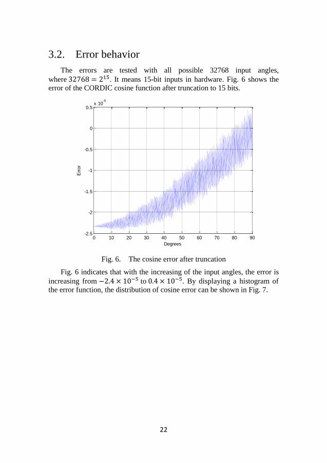
Error behavior 3.2.
The errors are tested with all possible 32768 input angles,
where 32768 = 215. It means 15-bit inputs in hardware. Fig. 6 shows the
error of the CORDIC cosine function after truncation to 15 bits.
Fig. 6. The cosine error after truncation
Fig. 6 indicates that with the increasing of the input angles, the error is
increasing from −2.4 × 10⁻⁵ to 0.4 × 10⁻⁵. By displaying a histogram of
the error function, the distribution of cosine error can be shown in Fig. 7.
0 10 20 30 40 50 60 70 80 90-2.5
-2
-1.5
-1
-0.5
0
0.5x 10
-5
Err
or
Degrees

23
Fig. 7. The cosine error distribution
Fig. 7 indicates that the cosine error peak is placed at −2.4 × 10⁻⁵ .
Most of the errors are placed away from zero, which is a drawback. The
absolute cosine error in dB is shown in Fig. 8.
Fig. 8. The absolute cosine error in dB
-2.5 -2 -1.5 -1 -0.5 0 0.5
x 10-5
0
500
1000
1500
2000
2500
3000
3500
4000
4500
Num
ber
of
err
ors
Error
0 10 20 30 40 50 60 70 80 90-200
-180
-160
-140
-120
-100
-80
The a
bsolu
te c
osin
e e
rror
in d
B
Degrees
24
Since the combination of binary numbers and decibel (dB) matches
very well, displaying the errors in dB can simplify the understanding of the
errors. The errors in dB are shown in (15), where 𝑥 is the error.
𝑥𝑑𝐵 = 20𝑙𝑜𝑔10|𝑥| (15)
Accuracy 3.3.
In binary, one bit can presents 2 results, 0 and 1. That is, 20𝑙𝑜𝑔10(2) ≈6𝑑𝐵 corresponds to 1 binary bit in resolution. The logarithmic error divided
by −20𝑙𝑜𝑔10(2) gives the number of the bits, as shown in (16).
𝑛 = −𝑥𝑑𝐵 20𝑙𝑜𝑔10(2)⁄ (16)
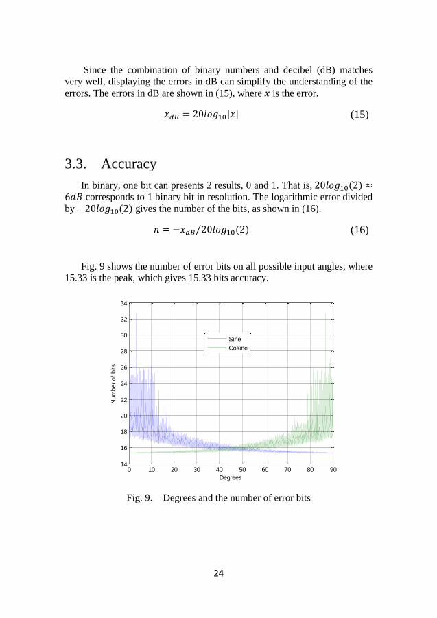
Fig. 9 shows the number of error bits on all possible input angles, where
15.33 is the peak, which gives 15.33 bits accuracy.
Fig. 9. Degrees and the number of error bits
0 10 20 30 40 50 60 70 80 9014
16
18
20
22
24
26
28
30
32
34
Degrees
Num
ber
of
bits
Sine
Cosine

25
4. Hardware implementation
In this section, the design flow for the thesis and the five different
unrolled CORDIC architectures are implemented in hardware.
IO65LPHVT_SF_1V8_50A_7M4X0Y2Z_nom_1.00V_1.80V_25C.db and
CORE65LPHVT_nom_1.20V_25C.db are the libraries used in design
compiler and prime time. In other words, a low power high VT (LPHVT)
technology is used at a supply voltage at 1.2V.
Design flow 4.1.
Design requirements
Matlab simualtion
RTL simulation
verfication
synthesis
Post synthesis verfication
Power analysis
Matlab
ModelSim
Matlab
Design complier
ModelSim
Primetime tool
Fig. 10. The design flow
Fig. 10 shows the design flow for the thesis. To implement the
CORDIC design in hardware, it should be starting with the MATLAB
simulation. The design is coded in VHDL after that the MATLAB model
26
satisfies the requirements of the design. By using ModelSim to simulate the
VHDL code, the result will be compared to the MATLAB model. A netlist
and a Value Change Dump (VCD) file are generated by design complier and
ModelSim separately, which are used for power analysis with the primetime
tool.
Hardware architectures and simulation results 4.2.
In this section, five different CORDIC architectures are implemented in
hardware. One is the original CORDIC architecture. The other four
architectures reduce the complexity in different levels.
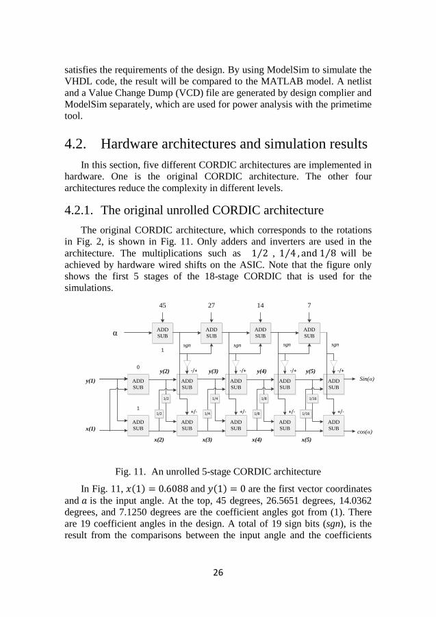
4.2.1. The original unrolled CORDIC architecture
The original CORDIC architecture, which corresponds to the rotations
in Fig. 2, is shown in Fig. 11. Only adders and inverters are used in the
architecture. The multiplications such as 1 2⁄ , 1 4⁄ , and 1 8⁄ will be
achieved by hardware wired shifts on the ASIC. Note that the figure only
shows the first 5 stages of the 18-stage CORDIC that is used for the
simulations.
ADD
SUB
ADD
SUB
ADD
SUB
ADD
SUBα
45 27 14 7
ADD
SUB
ADD
SUB
ADD
SUB
ADD
SUB
ADD
SUB
ADD
SUB
ADD
SUB
ADD
SUB
ADD
SUB
ADD
SUB
y(1)
x(1)
1/2
1/2
1/4
1/4
1/8
1/8
1/16
1/16
1
0
1
-/+
+/-
-/+
+/-
-/+ -/+
+/- +/-
sgn sgn sgn sgn
Sin(α)
cos(α)
x(2) x(3) x(4) x(5)
y(2) y(3) y(4) y(5)
Fig. 11. An unrolled 5-stage CORDIC architecture
In Fig. 11, 𝑥(1) = 0.6088 and 𝑦(1) = 0 are the first vector coordinates
and 𝑎 is the input angle. At the top, 45 degrees, 26.5651 degrees, 14.0362
degrees, and 7.1250 degrees are the coefficient angles got from (1). There
are 19 coefficient angles in the design. A total of 19 sign bits (sgn), is the
result from the comparisons between the input angle and the coefficients
27
angle, which is obtained in the upper adder row. The middle and the lower
adder row compute the approximations from the left to the right, where the
output is generated. The sign bits determine if the middle and the lower row
should be added or subtracted.
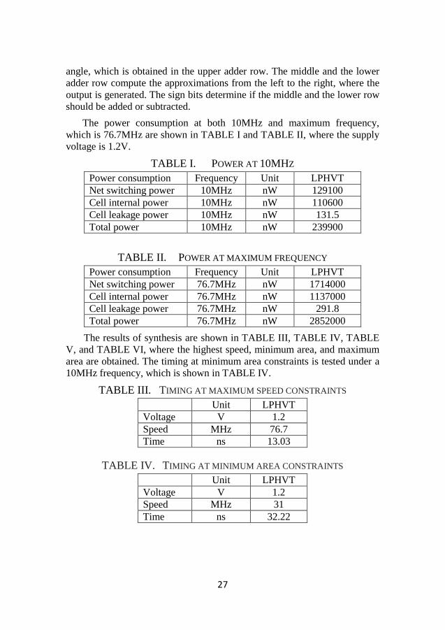
The power consumption at both 10MHz and maximum frequency,
which is 76.7MHz are shown in TABLE I and TABLE II, where the supply
voltage is 1.2V.
POWER AT 10MHZ TABLE I.
Power consumption Frequency Unit LPHVT
Net switching power 10MHz nW 129100
Cell internal power 10MHz nW 110600
Cell leakage power 10MHz nW 131.5
Total power 10MHz nW 239900
POWER AT MAXIMUM FREQUENCY TABLE II.
Power consumption Frequency Unit LPHVT
Net switching power 76.7MHz nW 1714000
Cell internal power 76.7MHz nW 1137000
Cell leakage power 76.7MHz nW 291.8
Total power 76.7MHz nW 2852000
The results of synthesis are shown in TABLE III, TABLE IV, TABLE
V, and TABLE VI, where the highest speed, minimum area, and maximum
area are obtained. The timing at minimum area constraints is tested under a
10MHz frequency, which is shown in TABLE IV.
TIMING AT MAXIMUM SPEED CONSTRAINTS TABLE III.
Unit LPHVT
Voltage V 1.2
Speed MHz 76.7
Time ns 13.03
TIMING AT MINIMUM AREA CONSTRAINTS TABLE IV.
Unit LPHVT
Voltage V 1.2
Speed MHz 31
Time ns 32.22
28
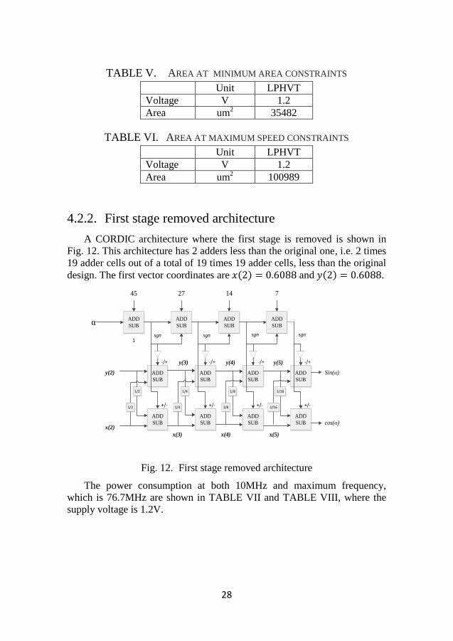
AREA AT MINIMUM AREA CONSTRAINTS TABLE V.
Unit LPHVT
Voltage V 1.2
Area um2
35482
AREA AT MAXIMUM SPEED CONSTRAINTS TABLE VI.
Unit LPHVT
Voltage V 1.2
Area um2 100989
4.2.2. First stage removed architecture
A CORDIC architecture where the first stage is removed is shown in
Fig. 12. This architecture has 2 adders less than the original one, i.e. 2 times
19 adder cells out of a total of 19 times 19 adder cells, less than the original
design. The first vector coordinates are 𝑥(2) = 0.6088 and 𝑦(2) = 0.6088.
ADD
SUB
ADD
SUB
ADD
SUB
ADD
SUBα
45 27 14 7
ADD
SUB
ADD
SUB
ADD
SUB
ADD
SUB
ADD
SUB
ADD
SUB
ADD
SUB
ADD
SUB
y(2)
x(2)
1/2
1/2
1/4
1/4
1/8
1/8
1/16
1/16
1
-/+
+/-
-/+
+/-
-/+ -/+
+/- +/-
sgn sgn sgn sgn
Sin(α)
cos(α)
x(3) x(4) x(5)
y(3) y(4) y(5)
Fig. 12. First stage removed architecture
The power consumption at both 10MHz and maximum frequency,
which is 76.7MHz are shown in TABLE VII and TABLE VIII, where the
supply voltage is 1.2V.
29
POWER AT 10MHZ TABLE VII.
Power consumption Frequency Unit LPHVT
Net switching power 10MHz nW 121700
Cell internal power 10MHz nW 104500
Cell leakage power 10MHz nW 131.5
Total power 10MHz nW 226300
POWER AT MAXIMUM FREQUENCY TABLE VIII.
Power consumption Frequency Unit LPHVT
Net switching power 76.7MHz nW 1692000
Cell internal power 76.7MHz nW 1109000
Cell leakage power 76.7MHz nW 296.2
Total power 76.7MHz nW 2802000
The results of synthesis are shown in TABLE IX, TABLE X, TABLE
XI, and TABLE XII, where the highest speed, minimum area, and
maximum area are obtained.
TIMING AT MAXIMUM SPEED CONSTRAINTS TABLE IX.
Unit LPHVT
Voltage V 1.2
Speed MHz 76.7
Time ns 13.03
TIMING AT MINIMUM AREA CONSTRAINTS TABLE X.
Unit LPHVT
Voltage V 1.2
Speed MHz 31
Time ns 32.21
AREA AT MINIMUM AREA CONSTRAINTS TABLE XI.
Unit LPHVT
Voltage V 1.2
Area um2
35394
AREA AT MAXIMUM SPEED CONSTRAINTS TABLE XII.
Unit LPHVT
Voltage V 1.2
Area um2 100484
30
4.2.3. Two stages eliminated architecture
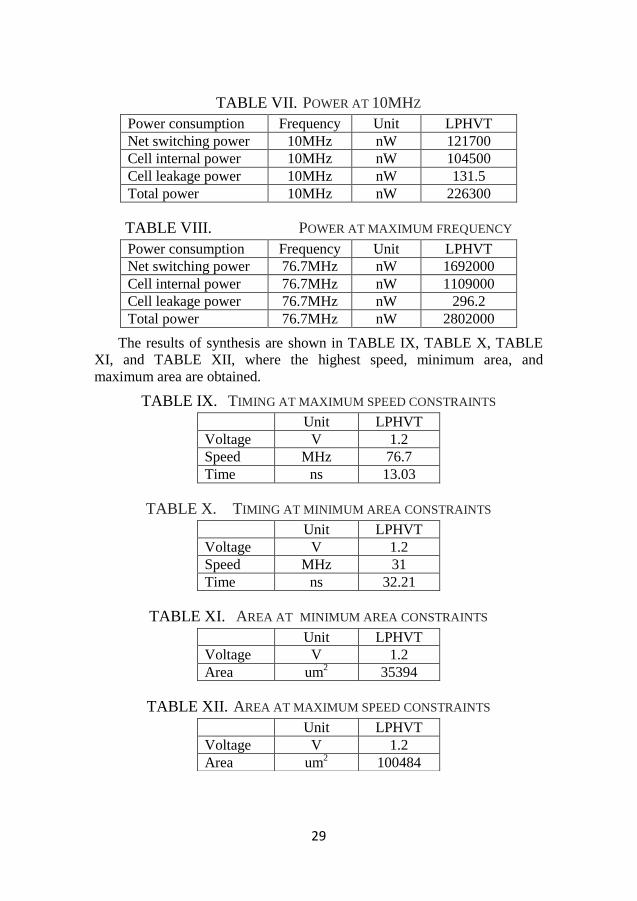
A CORDIC architecture where two stages are removed is shown in Fig.
13, which corresponds to the rotations in Fig. 3. This architecture has four
adders less than the original one. Two of these adders are replaced by two
MUXes, which are controlled by the first sgn bit in the upper adder row.
The two hardware wired shifts (1/2) are also removed compared to the
original architecture. As described in section 2.2, the first vector coordinates
(𝑥(3), 𝑦(3)) are shown in (8) and (9).
ADD
SUB
ADD
SUB
ADD
SUB
ADD
SUBα
45 27 14 7
ADD
SUB
ADD
SUB
ADD
SUB
ADD
SUB
ADD
SUB
ADD
SUB
1/4
1/4
1/8
1/8
1/16
1/16
1
-/+
+/-
-/+ -/+
+/- +/-
sgn sgn sgn sgn
Sin(α)
cos(α)
1
0
1
0
y(3)1
x(3)1
y(4)
x(4)
y(5)
x(5)
y(3)2
x(3)2
Fig. 13. Two stages are removed in the architecture
The power consumption at both 10MHz and maximum frequency,
which is 83.1MHz are shown in TABLE XIII and TABLE XIV, where the
supply voltage is 1.2V.
POWER AT 10MHZ TABLE XIII.
Power consumption at Frequency Unit LPHVT
Net switching power 10MHz nW 115700
Cell internal power 10MHz nW 96490
Cell leakage power 10MHz nW 126.2
Total power 10MHz nW 212400
31
POWER AT MAXIMUM FREQUENCY TABLE XIV.
Power consumption at Frequency Unit LPHVT
Net switching power 83.1MHz nW 1615000
Cell internal power 83.1MHz nW 1071000
Cell leakage power 83.1MHz nW 319.2
Total power 83.1MHz nW 2687000
The results of the synthesis are shown in TABLE XV, TABLE XVI,
TABLE XVII, and TABLE XVIII, where the highest speed and minimum
area, are obtained.
TIMING AT MAXIMUM SPEED CONSTRAINTS TABLE XV.
Unit LPHVT
Voltage V 1.2
Speed MHz 83.1
Time ns 12.03
TIMING AT MINIMUM AREA CONSTRAINTS TABLE XVI.
Unit LPHVT
Voltage V 1.2
Speed MHz 31.5
Time ns 31.78
AREA AT MINIMUM AREA CONSTRAINTS TABLE XVII.
Unit LPHVT
Voltage V 1.2
Area um2
33660
AREA AT MAXIMUM SPEED CONSTRAINTS TABLE XVIII.
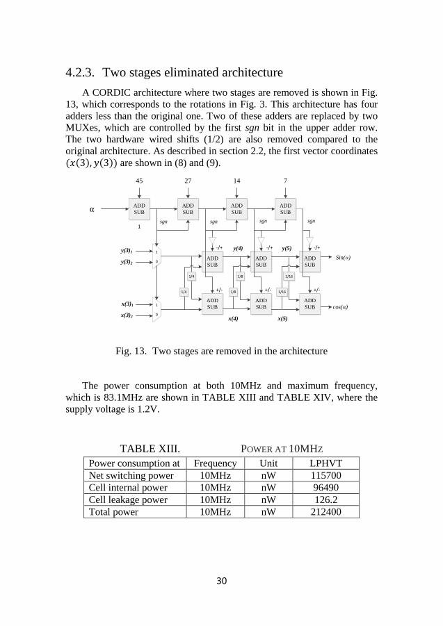
4.2.4. Three stages eliminated architecture
A CORDIC architecture where three stages are removed is shown in
Fig. 14, which corresponds to the rotations in Fig. 4. This architecture has 6
adders less than the original one. Four of these adders are replaced by six
MUXes, which are controlled by the first two sgns in the upper adder row.
As described in section 2.3, the first vector coordinates (𝑥(4), 𝑦(4)) are
shown in (11), (12), (13), and (14).
Unit LPHVT
Voltage V 1.2
Area um2 109840
32
ADD
SUB
ADD
SUB
ADD
SUB
ADD
SUBα
45 27 14 7
ADD
SUB
ADD
SUB
ADD
SUB
ADD
SUB
1/8
1/8
1/16
1/16
1
-/+ -/+
+/- +/-
sgn sgn sgn sgn
Sin(α)
cos(α)
1
0
y(3)1
x(3)1
y(4)
x(4)
y(5)
x(5)
y(3)2
x(3)2
1
0
10
10
10
10
y(3)3
y(3)4
x(3)3
x(3)4
Fig. 14. Three stages are removed architecture
The power consumption at both 10MHz and maximum frequency,
which is 90.7MHz are shown in TABLE XIX and TABLE XX, where the
supply voltage is 1.2V.
POWER AT 10MHZ TABLE XIX.
Power consumption Frequency Unit LPHVT
Net switching power 10MHz nW 97410
Cell internal power 10MHz nW 88820
Cell leakage power 10MHz nW 123.5
Total power 10MHz nW 186400
POWER AT MAXIMUM FREQUENCY TABLE XX.
Power consumption Frequency Unit LPHVT
Net switching power 90.7MHz nW 1396000
Cell internal power 90.7MHz nW 922900
Cell leakage power 90.7MHz nW 308.8
Total power 90.7MHz nW 2319000
The results of synthesis are shown in TABLE XXI, TABLE XXII,
TABLE XXIII, and TABLE XXIV, where the highest speed, minimum area,
and maximum area are obtained.
TIMING AT MAXIMUM SPEED CONSTRAINTS TABLE XXI.
Unit LPHVT
Voltage V 1.2
Speed MHz 90.7
Time ns 11.03
33
TIMING AT MINIMUM AREA CONSTRAINTS TABLE XXII.
Unit LPHVT
Voltage V 1.2
Speed MHz 32.3
Time ns 30.93
AREA AT MINIMUM AREA CONSTRAINTS TABLE XXIII.
Unit LPHVT
Voltage V 1.2
Area um2
33407
AREA AT MAXIMUM SPEED CONSTRAINTS TABLE XXIV.
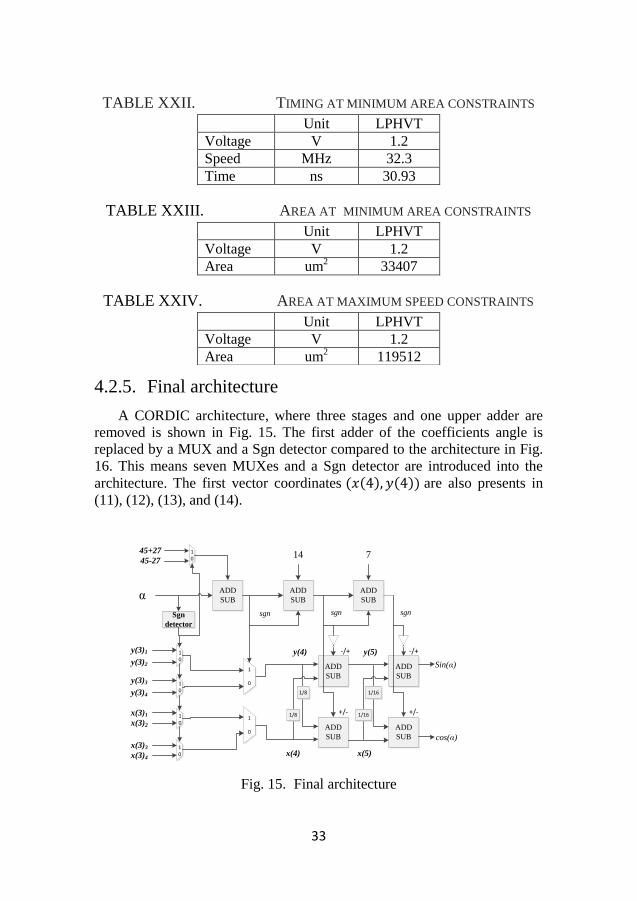
4.2.5. Final architecture
A CORDIC architecture, where three stages and one upper adder are
removed is shown in Fig. 15. The first adder of the coefficients angle is
replaced by a MUX and a Sgn detector compared to the architecture in Fig.
16. This means seven MUXes and a Sgn detector are introduced into the
architecture. The first vector coordinates (𝑥(4), 𝑦(4)) are also presents in
(11), (12), (13), and (14).
Sgn
detector
ADD
SUB
ADD
SUB
ADD
SUBα
14 7
ADD
SUB
ADD
SUB
ADD
SUB
ADD
SUB
1/8
1/8
1/16
1/16
-/+ -/+
+/- +/-
sgn sgn sgn
Sin(α)
cos(α)
1
0
y(3)1
x(3)1
y(4)
x(4)
y(5)
x(5)
y(3)2
x(3)2
1
0
10
10
10
10
y(3)3
y(3)4
x(3)3
x(3)4
10
45+27
45-27
Fig. 15. Final architecture
Unit LPHVT
Voltage V 1.2
Area um2 119512
34
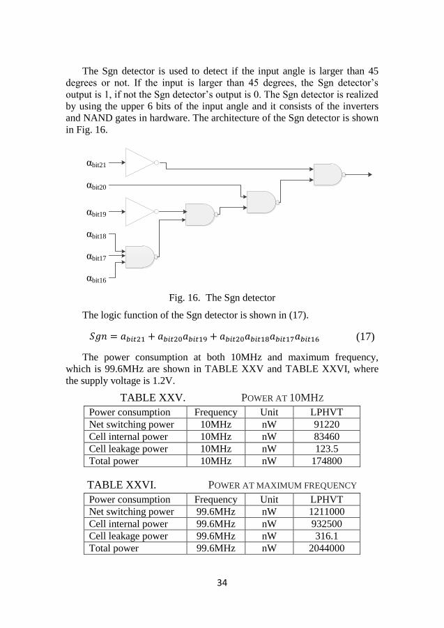
The Sgn detector is used to detect if the input angle is larger than 45
degrees or not. If the input is larger than 45 degrees, the Sgn detector’s
output is 1, if not the Sgn detector’s output is 0. The Sgn detector is realized
by using the upper 6 bits of the input angle and it consists of the inverters
and NAND gates in hardware. The architecture of the Sgn detector is shown
in Fig. 16.
αbit21
αbit20
αbit19
αbit18
αbit17
αbit16
Fig. 16. The Sgn detector
The logic function of the Sgn detector is shown in (17).
𝑆𝑔𝑛 = 𝑎𝑏𝑖𝑡21 + 𝑎𝑏𝑖𝑡20𝑎𝑏𝑖𝑡19 + 𝑎𝑏𝑖𝑡20𝑎𝑏𝑖𝑡18𝑎𝑏𝑖𝑡17𝑎𝑏𝑖𝑡16 (17)
The power consumption at both 10MHz and maximum frequency,
which is 99.6MHz are shown in TABLE XXV and TABLE XXVI, where
the supply voltage is 1.2V.
POWER AT 10MHZ TABLE XXV.
Power consumption Frequency Unit LPHVT
Net switching power 10MHz nW 91220
Cell internal power 10MHz nW 83460
Cell leakage power 10MHz nW 123.5
Total power 10MHz nW 174800
POWER AT MAXIMUM FREQUENCY TABLE XXVI.
Power consumption Frequency Unit LPHVT
Net switching power 99.6MHz nW 1211000
Cell internal power 99.6MHz nW 932500
Cell leakage power 99.6MHz nW 316.1
Total power 99.6MHz nW 2044000
35
The results of synthesis are shown in TABLE XXVII, TABLE XXVIII,
TABLE XXIX, and TABLE XXX, where the highest speed, minimum area,
and maximum area are obtained.
TIMING AT MAXIMUM SPEED CONSTRAINTS TABLE XXVII.
Unit LPHVT
Voltage V 1.2
Speed MHz 99.6
Time ns 10.04
TIMING AT MINIMUM AREA CONSTRAINTS TABLE XXVIII.
Unit LPHVT
Voltage V 1.2
Speed MHz 32.3
Time ns 30.95
AREA AT MINIMUM AREA CONSTRAINTS TABLE XXIX.
Unit LPHVT
Voltage V 1.2
Area um2
33394
AREA AT MAXIMUM SPEED CONSTRAINTS TABLE XXX.
Unit LPHVT
Voltage V 1.2
Area um2 135193

36
37
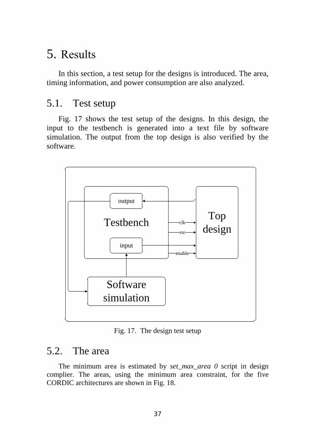
5. Results
In this section, a test setup for the designs is introduced. The area,
timing information, and power consumption are also analyzed.
Test setup 5.1.
Fig. 17 shows the test setup of the designs. In this design, the
input to the testbench is generated into a text file by software
simulation. The output from the top design is also verified by the
software.
TestbenchTop
design
input
output
rst
clk
enable
Software
simulation
Fig. 17. The design test setup
The area 5.2.
The minimum area is estimated by set_max_area 0 script in design
complier. The areas, using the minimum area constraint, for the five
CORDIC architectures are shown in Fig. 18.

38
Fig. 18. Area at different frequencies
The minimum areas can be shown in TABLE XXXI. The final
architecture has the lowest area, 33200um2.
AREA AT MINIMUM AREA CONSTRAINTS TABLE XXXI.
Architectures Minimum area (um2)
The original architecture 36067
First stage eliminated architecture 35966
Two stages eliminated architecture 33999
Three stages eliminated architecture 33389
Final architecture 33200
TABLE XXXI indicates that with reduced complexity, the minimum
areas of the designs are also reduced. The percentage of the area reduction is
7.9%. The areas at maximum speed constraints for the five architectures are
shown in TBALE XXXII.
0 10 20 30 40 50 60 70 80 90 1002
4
6
8
10
12
14x 10
4
Fequency (MHz)
are
a (
um
2)
Origianal architecture
First stage eliminated architecture
Two stages eliminated architecture
Three stages eliminated architecture
Final architecture
39
AREA AT MAXIMUM SPEED CONSTRAINTS TABLE XXXII.
Architectures Area (um2)
The original architecture 100989
First stage eliminated architecture 100484
Two stages eliminated architecture 109840
Three stages eliminated architecture 119512
Final architecture 135193
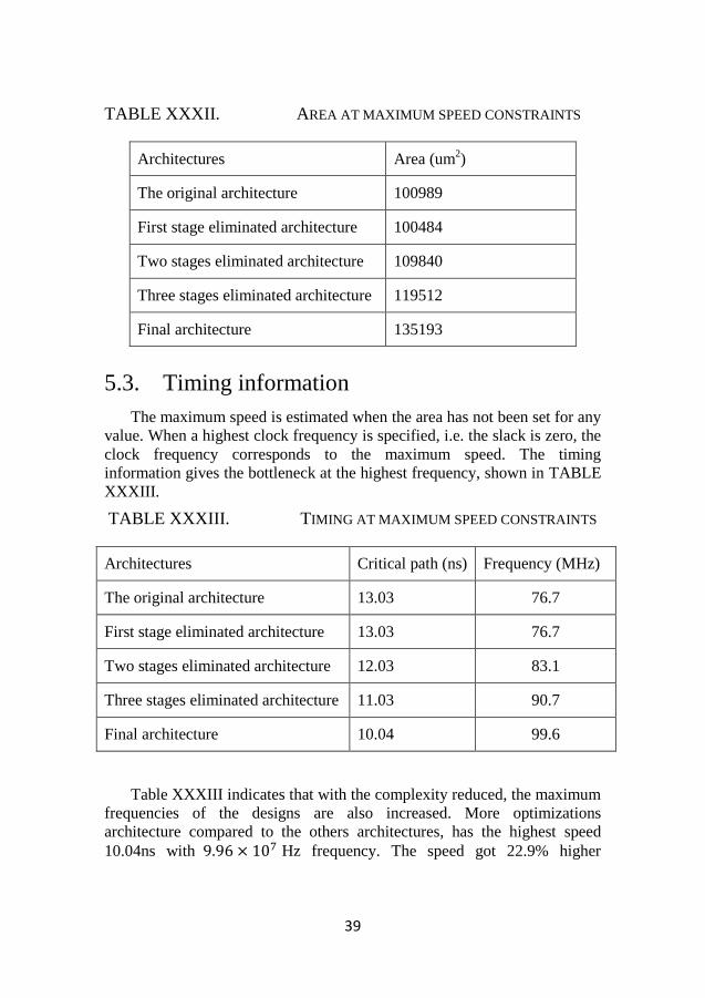
Timing information 5.3.
The maximum speed is estimated when the area has not been set for any
value. When a highest clock frequency is specified, i.e. the slack is zero, the
clock frequency corresponds to the maximum speed. The timing
information gives the bottleneck at the highest frequency, shown in TABLE
XXXIII.
TIMING AT MAXIMUM SPEED CONSTRAINTS TABLE XXXIII.
Architectures Critical path (ns) Frequency (MHz)
The original architecture 13.03 76.7
First stage eliminated architecture 13.03 76.7
Two stages eliminated architecture 12.03 83.1
Three stages eliminated architecture 11.03 90.7
Final architecture 10.04 99.6
Table XXXIII indicates that with the complexity reduced, the maximum
frequencies of the designs are also increased. More optimizations
architecture compared to the others architectures, has the highest speed
10.04ns with 9.96 × 10⁷ Hz frequency. The speed got 22.9% higher

40
performance. The timing at minimum area constraints are shown in
TABLEXXXIV.
TIMING AT MINIMUM AREA CONSTRAINTS TABLE XXXIV.
Architectures Time (ns) Speed (MHz)
The original architecture 32.22 31
First stage eliminated architecture 32.21 31
Two stages eliminated architecture 31.78 31.5
Three stages eliminated architecture 30.93 32.3
Final architecture 30.95 32.3
Power consumption 5.4.
5.4.1. Power analysis
The CMOS transistors’ power consists of dynamic power and static
power, as shown in (18) [6].
𝑃𝑡𝑜𝑡 = 𝑃𝑑𝑦𝑛𝑎𝑚𝑖𝑐 + 𝑃𝑠𝑡𝑎𝑡𝑖𝑐 (18)
The dynamic power consists of the switching power and the internal
power, as shown in (19).
𝑃𝑑𝑦𝑛𝑎𝑚𝑖𝑐 = 𝑃𝑠𝑤𝑖𝑡𝑐ℎ𝑖𝑛𝑔 + 𝑃𝑖𝑛𝑡𝑒𝑟𝑛𝑎𝑙 (19)
The dynamic power can be written in (20).
𝑃𝑑𝑦𝑛𝑎𝑚𝑖𝑐 = 𝑎𝐶𝑉2𝑓 (20)
Where the factor 𝑎 is the switching activity, 𝐶 is the node capacitance, 𝑓
is the clock frequency, and 𝑉 is the supply voltage. The static power comes
mainly from the sub threshold leakage current.
41
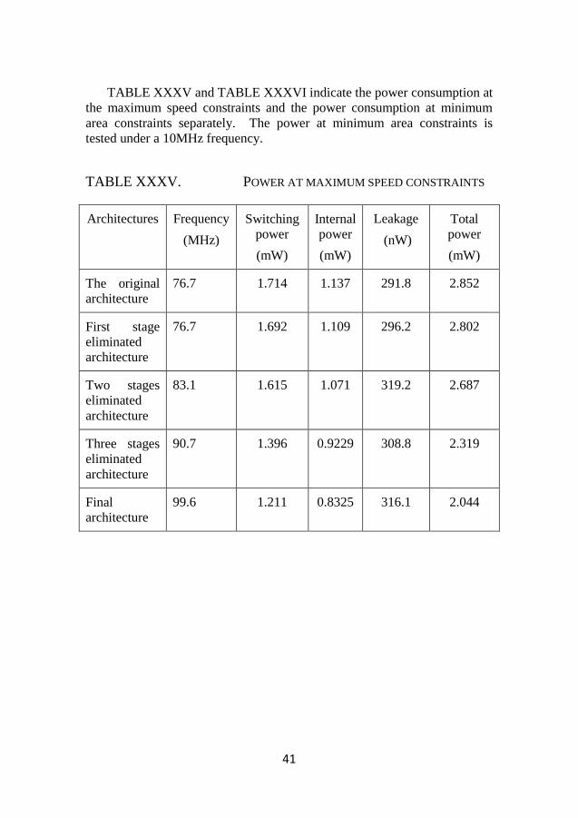
TABLE XXXV and TABLE XXXVI indicate the power consumption at
the maximum speed constraints and the power consumption at minimum
area constraints separately. The power at minimum area constraints is
tested under a 10MHz frequency.
POWER AT MAXIMUM SPEED CONSTRAINTS TABLE XXXV.
Architectures Frequency
(MHz)
Switching
power
(mW)
Internal
power
(mW)
Leakage
(nW)
Total
power
(mW)
The original
architecture
76.7 1.714 1.137 291.8 2.852
First stage
eliminated
architecture
76.7 1.692 1.109 296.2 2.802
Two stages
eliminated
architecture
83.1 1.615 1.071 319.2 2.687
Three stages
eliminated
architecture
90.7 1.396 0.9229 308.8 2.319
Final
architecture
99.6 1.211 0.8325 316.1 2.044
42
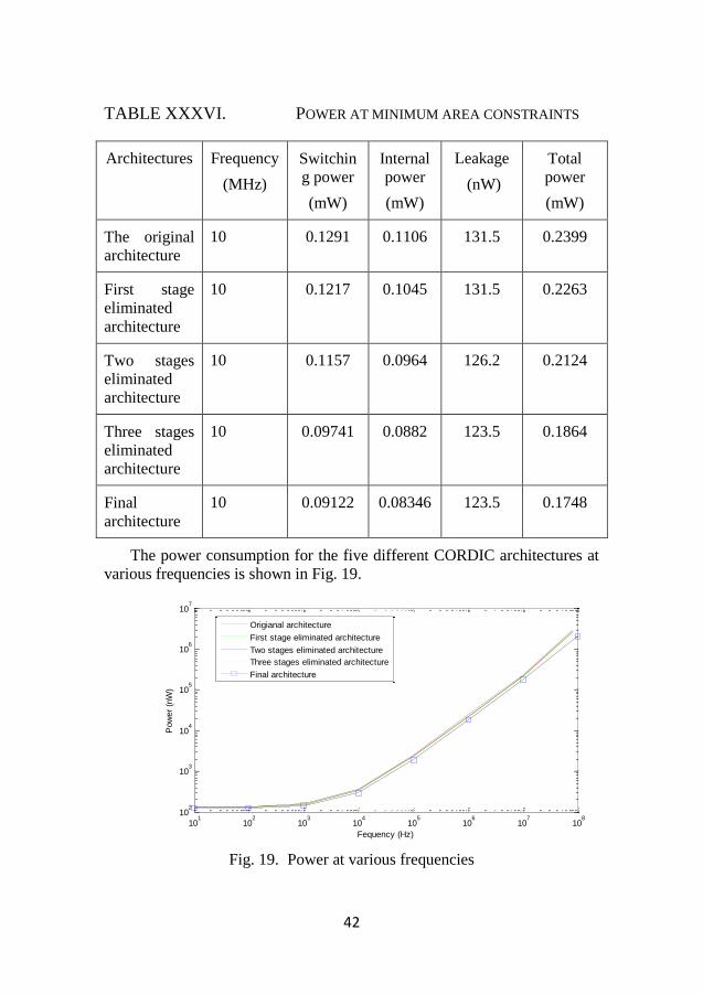
POWER AT MINIMUM AREA CONSTRAINTS TABLE XXXVI.
Architectures Frequency
(MHz)
Switchin
g power
(mW)
Internal
power
(mW)
Leakage
(nW)
Total
power
(mW)
The original
architecture
10 0.1291 0.1106 131.5 0.2399
First stage
eliminated
architecture
10 0.1217 0.1045 131.5 0.2263
Two stages
eliminated
architecture
10 0.1157 0.0964 126.2 0.2124
Three stages
eliminated
architecture
10 0.09741 0.0882 123.5 0.1864
Final
architecture
10 0.09122 0.08346 123.5 0.1748
The power consumption for the five different CORDIC architectures at
various frequencies is shown in Fig. 19.
Fig. 19. Power at various frequencies
101
102
103
104
105
106
107
108
102
103
104
105
106
107
Fequency (Hz)
Pow
er
(nW
)
Origianal architecture
First stage eliminated architecture
Two stages eliminated architecture
Three stages eliminated architecture
Final architecture
43
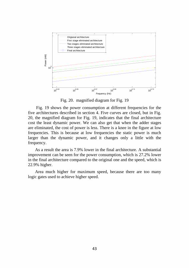
Fig. 20. magnified diagram for Fig. 19
Fig. 19 shows the power consumption at different frequencies for the
five architectures described in section 4. Five curves are closed, but in Fig.
20, the magnified diagram for Fig. 19, indicates that the final architecture
cost the least dynamic power. We can also get that when the adder stages
are eliminated, the cost of power is less. There is a knee in the figure at low
frequencies. This is because at low frequencies the static power is much
larger than the dynamic power, and it changes only a little with the
frequency.
As a result the area is 7.9% lower in the final architecture. A substantial
improvement can be seen for the power consumption, which is 27.2% lower
in the final architecture compared to the original one and the speed, which is
22.9% higher.
Area much higher for maximum speed, because there are too many
logic gates used to achieve higher speed.
106.63
106.65
106.67
106.69
106.71
106.73
105
Fequency (Hz)
Pow
er
(nW
)
Origianal architecture
First stage eliminated architecture
Two stages eliminated architecture
Three stages eliminated architecture
Final architecture

44
45
6. Conclusions
In this thesis, MUXes are used in hardware to reduce the complexity.
Five different CORIDC architectures are implemented with eliminating the
stages. The area, computational speed, accuracy, error behavior, and the
power consumption have been analyzed under the software simulation and
hardware implementation. The speed, minimum area and power
consumption have got optimized in different levels. As a result the area and
power consumption get 7.9% lower and 27.2% lower separately, and the
speed is 22.9% higher compared to the original unrolled CORDIC
architecture. It is also proved that in unrolled CORDIC architectures, the
reduction of the power consumption can be achieved by reducing the
complexity, which meets the aim of this thesis.

46

47
7. Future work
In this thesis, three stages are eliminated at most. There are more stages
can be eliminated for the reduction of the power consumption.
More than one Sgn detector can be introduced to reduce the coefficients
adder.
The number of the iteration should decrease to some extent, which can
also reduce the power consumption.

48
49
References
[1] Erik Hertz and Peter Nilsson, “Parabolic Synthesis Methodology
Implemented on the Sine Function”, in Proceedings of the 2009
International Symposium on Circuits and Systems (ISCAS’09), Taipei,
Taiwan, May 2427, 2009 .
[2] Gordon K. Smyth “Polynomial Approximation” in Encyclopedia of
Biostatistics ,John Wiley & Sons, Ltd, Chichester, Peter Armitage and
Theodore Colton, (ISBN 0471 975761) ,1998.
[3] J. E. Volder, “The CORDIC Trigonometric Computing Technique”,
IRE Transactions on Electronic Computers, vol. EC-8, no. 3, 1959, pp.
330–334.
[4] Hue, Y.H., “CORDIC-based VLSI architectures for digital signal
processing”, IEEE Signal Processing Magazine, pp. 16-35, ISSN:
1053-5888, July 1992.
[5] Peter Nilsson “Complexity Reductions in Unrolled CORDIC
Architectures,” in Proceedings of the IEEE 14th International
Conference on Electronics, Circuits and Systems (ICECS 2009), pp.
868-871, Hammamet, Tunisia, December 13-16, 2009.
[6] http://en.wikipedia.org/wiki/CMOS#Power:_switching_and_leakage

50

51
Appendix A COEFFICIENT ANGLES TABLE XXXVII.
Decimal angle Binary angle
α1 45 00101101000000000000000
α2 26.565032958984375 00011010100100001010011
α3 14.036224365234375 00001110000010010100011
α4 7.125000000000000 00000111001000000000000
α5 3.576324462890625 00000011100100111000101
α6 1.789886474609375 00000001110010100011011
α7 0.895172119140625 00000000111001010010101
α8 0.447601318359375 00000000011100101001011
α9 0.223785400390625 00000000001110010100101
α10 0.111877441406250 00000000000111001010010
α11 0.055938720703125 00000000000011100101001
α12 0.027954101562500 00000000000001110010100
α13 0.013977050781250 00000000000000111001010
α14 0.006988525390625 00000000000000011100101
α15 0.003479003906250 00000000000000001110010
α16 0.001739501953125 00000000000000000111001
α17 0.000854492187500 00000000000000000011100
α18 0.000427246093750 00000000000000000001110
α19 0.000213623046875 00000000000000000000111

52


![AN EFFICIENT CORDIC PROCESSOR FOR COMPLEX DIGITAL … · CORDIC algorithm was first developed by Jack E. Volder in 1959 [1]. CORDIC algorithm is extremely useful in efficient and](https://static.fdocuments.us/doc/165x107/5e637e4912c3c2564c2cb16d/an-efficient-cordic-processor-for-complex-digital-cordic-algorithm-was-first-developed.jpg)