Compact controller with timer and ramp function
28
JUMO cTRON 04/08/16 Compact controller with timer and ramp function B 70.2070.2.0 Interface Description Modbus 2008-08-11/00492538 702071 702072 702074
Transcript of Compact controller with timer and ramp function
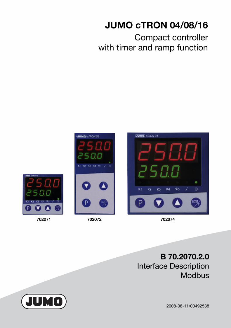
JUMO cTRON 04/08/16Compact controller
with timer and ramp function
B 70.2070.2.0Interface Description
Modbus
2008-08-11/00492538
702071 702072 702074


Contents
1 Introduction 5
1.1 Preface ........................................................................................................ 5
1.2 Typographical conventions ....................................................................... 5
2 Protocol description 7
2.1 Master-Slave principle ............................................................................... 7
2.2 Transmission mode (RTU) ......................................................................... 7
2.3 Device address ........................................................................................... 8
2.4 Timing of the communication ................................................................... 8
2.5 Structure of the data blocks ................................................................... 11
2.6 Function codes ......................................................................................... 122.6.1 Read n words ............................................................................................. 122.6.2 Write one word ........................................................................................... 132.6.3 Write n words ............................................................................................. 14
2.7 Transmission format (integer, float and text values) ............................. 15
2.8 Checksum (CRC16) .................................................................................. 17
2.9 Error processing ...................................................................................... 18
3 RS485 interface 19
3.1 Connection diagram ................................................................................ 19
3.2 Configuration ............................................................................................ 20
4 Modbus addresses 21
4.1 Process data ............................................................................................ 21
4.2 Set point values ........................................................................................ 23
4.3 Controller parameters ............................................................................. 23
4.4 Configuration ............................................................................................ 23
4.5 Commands ............................................................................................... 24
4.6 RAM memory ............................................................................................ 25

Contents
1 Introduction
1.1 PrefaceThis operating manual is addressed to the system manufacturer with adequatetechnical background and PC related knowledge.
Please read this operating manual prior to commissioning the device. Keepthe manual in a place accessible to all users at all times. Your comments areappreciated and may assist us in improving this manual.
All necessary settings are described in this operating manual. Shouldproblems be encountered during commissioning, please refrain from carryingout any manipulations that are not described in the manual. Any suchintervention will jeopardize your warranty rights. Please contact the nearestsubsidiary or the head office.
1.2 Typographical conventions
Warning signs:
Caution
Note signs:
Note
Reference
Number types:
Hexadecimal number
AThis symbol is used when there may be damage to equipment ordata if the instructions are ignored or not followed correctly!
H This symbol is used when your special attention is drawn to aremark.
vThis symbol refers to further information in other manuals,chapters or sections.
0x0010 A hexadecimal number is identified by „0x“ preceding the actualnumber (here: 16 decimal).
5

1 Introduction
6

2 Protocol description
2.1 Master-Slave principleCommunication between a master (e.g. PC) and a slave (e.g. measuring andcontrol system) using Modbus takes place according to the master-slaveprinciple, in the form of data request/instruction - response.
The master controls the data exchange, the slaves only have a responsefunction. They are identified by their device address.
2.2 Transmission mode (RTU)The transmission mode used is the RTU mode (Remote Terminal Unit). Data istransmitted in binary format (hexadecimal) with 8 bits. The LSB (leastsignificant bit) is transmitted first. The ASCII operating mode is not supported.
Data format The data format describes the structure of a character transmitted. Thefollowing data format options are available:
Master
Slave 1 Slave 2 Slave n
Data word Parity bit Stop bit1/2 bit
Number ofbits
8 bits — 1 9
8 bits even 1 10
8 bits odd 1 10
8 bits — 2 10
7
2 Protocol description
2.3 Device addressThe device address of the slave can be set between 0 and 254. Deviceaddress 0 is reserved.
There are two different forms of data exchange:
Query Data request/instruction by the master to a slave via the corresponding deviceaddress.
The slave addressed responds.
Broadcast Instruction by the master to all slaves via the device address 0 (e.g. to transmita specific value to all slaves).
The connected slaves do not respond. In such a case, the correct acceptanceof the value by the slaves should be checked by a subsequent readout at eachindividual slave.
Data request with the device address 0 is meaningless.
2.4 Timing of the communicationStart and end of a data block are marked by transmission pauses. Themaximum permitted interval between two consecutive characters is threetimes the transmission time required for a single character.
The character transmission time (time required to transmit one singlecharacter) depends on the baud rate and the data format used (stop bits andparity bit).
For a data format of 8 data bits, no parity bit and one stop bit, this is:
character transmission time [ms] = 1000 * 9 bit/baud rate
For the other data formats, this is:
character transmission time [ms]= 1000 * (8 bits+parity bit+stop bit(s)) bit/baud rate
H A maximum of 31 slaves can be addressed via the RS485 interface.
8

2 Protocol description
Timing
Example Marker for end of data request or end of response for a 10/9 bit data format
Waiting time = 3 characters * 1000 * 10 bit/baud rate
Data request from mastertransmission time = n characters * 1000 * x bit/baud rate
Marker for end of data request3 characters * 1000 * x bit/baud rate
Processing of data request by the slave (≤ 250ms)
Response of the slavetransmission time = n characters * 1000 * x bit/baud rate
Marker for end of response3 characters * 1000 * x bit/baud rate
Baud rate [baud] Data format [bit] Waiting time [ms](3 characters)
38400 10 0.79
9 0.71
19200 10 1.57
9 1.41
9600 10 3.13
9 2.82
9
2 Protocol description
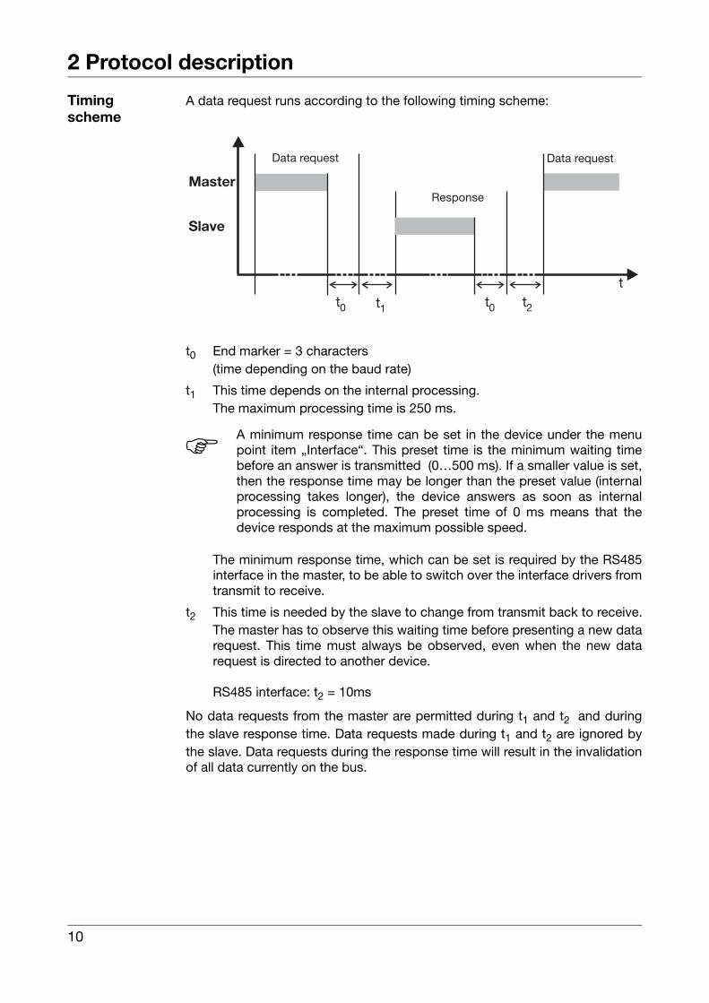
Timing scheme
A data request runs according to the following timing scheme:
t0 End marker = 3 characters (time depending on the baud rate)
t1 This time depends on the internal processing.The maximum processing time is 250 ms.
The minimum response time, which can be set is required by the RS485interface in the master, to be able to switch over the interface drivers fromtransmit to receive.
t2 This time is needed by the slave to change from transmit back to receive.The master has to observe this waiting time before presenting a new datarequest. This time must always be observed, even when the new datarequest is directed to another device.
RS485 interface: t2 = 10ms
No data requests from the master are permitted during t1 and t2 and duringthe slave response time. Data requests made during t1 and t2 are ignored bythe slave. Data requests during the response time will result in the invalidationof all data currently on the bus.
H A minimum response time can be set in the device under the menupoint item „Interface“. This preset time is the minimum waiting timebefore an answer is transmitted (0…500 ms). If a smaller value is set,then the response time may be longer than the preset value (internalprocessing takes longer), the device answers as soon as internalprocessing is completed. The preset time of 0 ms means that thedevice responds at the maximum possible speed.
Master
Slave
Data request
Response
t
Data request
t
0 t1 t2t0
10
2 Protocol description
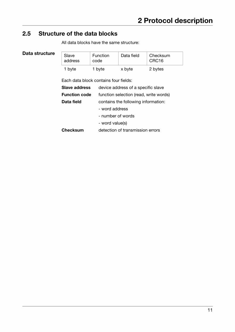
2.5 Structure of the data blocksAll data blocks have the same structure:
Data structure
Each data block contains four fields:
Slave address device address of a specific slave
Function code function selection (read, write words)
Data field contains the following information:
- word address
- number of words
- word value(s)
Checksum detection of transmission errors
Slaveaddress
Functioncode
Data field ChecksumCRC16
1 byte 1 byte x byte 2 bytes
11

2 Protocol description
2.6 Function codesThe functions described in the following are available for the readout ofmeasured values, device and process data as well as to write specific data.
Function-overview
2.6.1 Read n words
This function is used to read n (n ≤ 32) words starting from a specific address.
Data request
Response
Example Reading the W1 and W2 set point values (2 words each)
Address of first word = 0x3100 (W1 set point value)
Data request:
Response (values in the Modbus float format):
Functionnumber
Function Limitation
0x03 or 0x04 Read n words max. 32 words (64 bytes)0x06 Write one word max. 1 word (2 bytes)0x10 Write n words max. 32 words (64 bytes)
vPlease refer to Chapter 2.9 Error processing, Page 18 if the devicedoes not react to these functions or emits an error code.
Slaveaddress
Functionx03 or 0x04
Addressfirst word
Number ofwords(max. 32)
ChecksumCRC16
1 byte 1 byte 2 byte 2 byte 2 byte
Slaveaddress
Function0x03 or 0x04
Number ofbytes read
Wordvalue(s)
ChecksumCRC16
1 byte 1 byte 1 byte x byte 2 byte
01 03 3100 0004 4AF5
01 03 08 0000 41C8 0000 4120 4A9E
Set point value W1
(25.0)
Set point value W2
(10.0)
12
2 Protocol description
2.6.2 Write one word
For the Write Word function, the data blocks for instruction and response areidentical.
Instruction
Response
Example Write the limit value AL of limit comparator 1 = 275.0(Value = 0x80004389 in the Modbus float format)
Word address = 0x0057
Instruction: Write the first part of the value
Response (as instruction):
Instruction: Write the second part of the value (next word address)
Response (as instruction):
Slaveaddress
Function0x06
Word address Word value ChecksumCRC16
1 byte 1 byte 2 byte 2 bytes 2 byte
Slaveaddress
Function0x06
Word address Word value ChecksumCRC16
1 byte 1 byte 2 byte 2 byte 2 byte
01 06 0057 8000 59DA
01 06 0057 8000 59DA
01 06 0058 4389 F88F
01 06 0058 4389 F88F
13
2 Protocol description
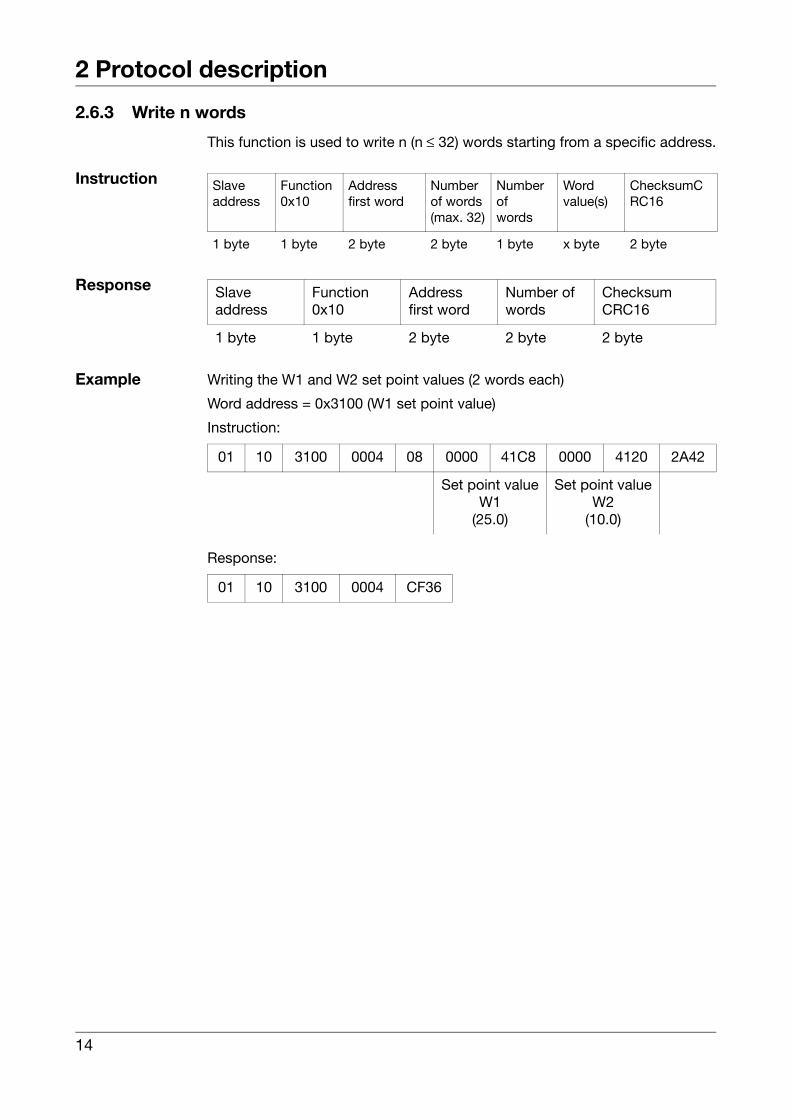
2.6.3 Write n words
This function is used to write n (n ≤ 32) words starting from a specific address.
Instruction
Response
Example Writing the W1 and W2 set point values (2 words each)
Word address = 0x3100 (W1 set point value)
Instruction:
Response:
Slaveaddress
Function0x10
Addressfirst word
Numberof words(max. 32)
Numberofwords
Wordvalue(s)
ChecksumCRC16
1 byte 1 byte 2 byte 2 byte 1 byte x byte 2 byte
Slave address
Function0x10
Addressfirst word
Number ofwords
ChecksumCRC16
1 byte 1 byte 2 byte 2 byte 2 byte
01 10 3100 0004 08 0000 41C8 0000 4120 2A42
Set point value W1
(25.0)
Set point value W2
(10.0)
01 10 3100 0004 CF36
14
2 Protocol description
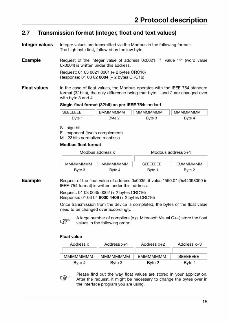
2.7 Transmission format (integer, float and text values)
Integer values Integer values are transmitted via the Modbus in the following format:The high byte first, followed by the low byte.
Example Request of the integer value of address 0x0021, if value "4" (word value0x0004) is written under this address.
Request: 01 03 0021 0001 (+ 2 bytes CRC16)Response: 01 03 02 0004 (+ 2 bytes CRC16)
Float values In the case of float values, the Modbus operates with the IEEE-754 standardformat (32bits), the only difference being that byte 1 and 2 are changed overwith byte 3 and 4.
Single-float format (32bit) as per IEEE 754standard
S - sign bitE - exponent (two's complement)M - 23bits normalized mantissa
Modbus float format
Example Request of the float value of address 0x0035, if value "550.0" (0x44098000 inIEEE-754 format) is written under this address.
Request: 01 03 0035 0002 (+ 2 bytes CRC16)Response: 01 03 04 8000 4409 (+ 2 bytes CRC16)
Once transmission from the device is completed, the bytes of the float valueneed to be changed over accordingly.
Float value
SEEEEEEE EMMMMMMM MMMMMMMM MMMMMMMM
Byte 1 Byte 2 Byte 3 Byte 4
Modbus address x Modbus address x+1
MMMMMMMM MMMMMMMM SEEEEEEE EMMMMMMM
Byte 3 Byte 4 Byte 1 Byte 2
H A large number of compilers (e.g. Microsoft Visual C++) store the floatvalues in the following order:
Address x Address x+1 Address x+2 Address x+3
MMMMMMMM MMMMMMMM EMMMMMMM SEEEEEEE
Byte 4 Byte 3 Byte 2 Byte 1
H Please find out the way float values are stored in your application.After the request, it might be necessary to change the bytes over inthe interface program you are using.
15
2 Protocol description
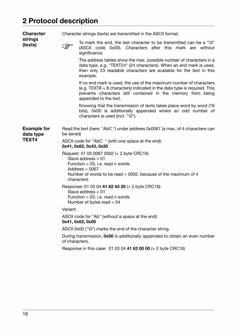
Character strings(texts)
Character strings (texts) are transmitted in the ASCII format.
Example for data type TEXT4
Read the text (here: "AbC ") under address 0x0067 (a max. of 4 characters canbe saved)
ASCII code for "AbC " (with one space at the end):0x41, 0x62, 0x43, 0x20
Request: 01 03 0067 0002 (+ 2 byte CRC16)Slave address = 01Function = 03, i.e. read n wordsAddress = 0067Number of words to be read = 0002, because of the maximum of 4characters
Response: 01 03 04 41 62 43 20 (+ 2 byte CRC16)Slave address = 01Function = 03, i.e. read n wordsNumber of bytes read = 04
Variant:
ASCII code for "Ab" (without a space at the end):0x41, 0x62, 0x00
ASCII 0x00 ("\0") marks the end of the character string.
During transmission, 0x00 is additionally appended to obtain an even numberof characters.
Response in this case: 01 03 04 41 62 00 00 (+ 2 byte CRC16)
H To mark the end, the last character to be transmitted can be a "\0"(ASCII code 0x00). Characters after this mark are withoutsignificance.
The address tables show the max. possible number of characters in adata type, e.g. "TEXT24" (24 characters). When an end mark is used,then only 23 readable characters are available for the text in thisexample.
If no end mark is used, the use of the maximum number of characters(e.g. TEXT8 = 8 characters) indicated in the data type is required. Thisprevents characters still contained in the memory from beingappended to the text.
Knowing that the transmission of texts takes place word by word (16bits), 0x00 is additionally appended where an odd number ofcharacters is used (incl. "\0").
16
2 Protocol description
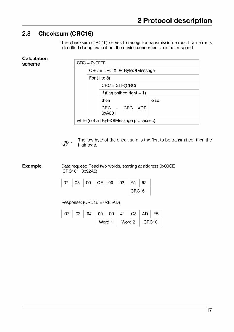
2.8 Checksum (CRC16)The checksum (CRC16) serves to recognize transmission errors. If an error isidentified during evaluation, the device concerned does not respond.
Calculation scheme
Example Data request: Read two words, starting at address 0x00CE(CRC16 = 0x92A5)
Response: (CRC16 = 0xF5AD)
CRC = 0xFFFF
CRC = CRC XOR ByteOfMessage
For (1 to 8)
CRC = SHR(CRC)
if (flag shifted right = 1)
then else
CRC = CRC XOR0xA001
while (not all ByteOfMessage processed);
H The low byte of the check sum is the first to be transmitted, then thehigh byte.
07 03 00 CE 00 02 A5 92
CRC16
07 03 04 00 00 41 C8 AD F5
Word 1 Word 2 CRC16
17
2 Protocol description
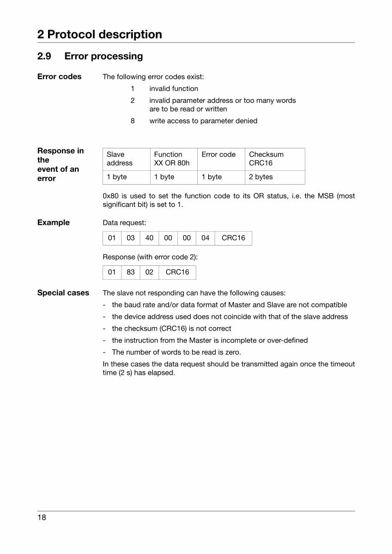
2.9 Error processing
Error codes The following error codes exist:
1 invalid function
2 invalid parameter address or too many wordsare to be read or written
8 write access to parameter denied
Response in theevent of an error
0x80 is used to set the function code to its OR status, i.e. the MSB (mostsignificant bit) is set to 1.
Example Data request:
Response (with error code 2):
Special cases The slave not responding can have the following causes:
- the baud rate and/or data format of Master and Slave are not compatible
- the device address used does not coincide with that of the slave address
- the checksum (CRC16) is not correct
- the instruction from the Master is incomplete or over-defined
- The number of words to be read is zero.
In these cases the data request should be transmitted again once the timeouttime (2 s) has elapsed.
Slaveaddress
FunctionXX OR 80h
Error code ChecksumCRC16
1 byte 1 byte 1 byte 2 bytes
01 03 40 00 00 04 CRC16
01 83 02 CRC16
18

3 RS485 interface
3.1 Connection diagram
Connection diagramType 702071
Connection diagramType 702072andType 702074
(1) RS485 interface
vThe devices of this controller series can be ordered with an RS485interface as an option. Please refer to the type sheet 70.2070 or theoperating manual B 70.2070.0 (type explanation) for the orderspecifications.
12
56
N(L-)L1(L+)
1413
17
20212223
RxD/TxD
1918
24(1)
-
+
H Connect the interface line shielding to earth on one side in theswitch cabinet.
12
56
N(L-)L1(L+)
1213
1516
17
20212223
RxD/TxD
1918
24(1)
-
+
19

3 RS485 interface
3.2 ConfigurationThe following table shows the possible Modbus interface settings to becarried out in the configuration level (ConF ➔ IntF) and/or in the setup program.
vFor more detailed information about configuration, please refer tooperating manual B 70.2070.0.
Symbol Value/Selection
Description
Baud rate bdrt 0
1
2
9600 bps
19200 bps
38400 bps
Data format dFt 0
1
2
3
8 data bits, 1 stop bit, no parity
8 data bits, 1 stop bit, odd parity
8 data bits, 1 stop bit, even parity
8 data bits, 2 stop bits, no parity
Device address Adr 0…1 …255 Address in data network
Addresses 0 and 255 are reserved for specificpurposes and should not be used here.
Minimumresponse time
(Setup) 0…500ms Minimum time period that elapses between therequest of a device in the data network and theresponse of the controller (can only be adjustedvia the setup program).
Factory settings are shown bold.
H When the communication takes place via the setup interface, theRS485 interface is inactive.
20
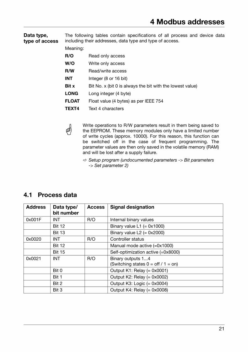
4 Modbus addresses
Data type,type of access
The following tables contain specifications of all process and device dataincluding their addresses, data type and type of access.
Meaning:
R/O Read only access
W/O Write only access
R/W Read/write access
INT Integer (8 or 16 bit)
Bit x Bit No. x (bit 0 is always the bit with the lowest value)
LONG Long integer (4 byte)
FLOAT Float value (4 bytes) as per IEEE 754
TEXT4 Text 4 characters
4.1 Process data
AWrite operations to R/W parameters result in them being saved tothe EEPROM. These memory modules only have a limited numberof write cycles (approx. 10000). For this reason, this function canbe switched off in the case of frequent programming. Theparameter values are then only saved in the volatile memory (RAM)and will be lost after a supply failure.
v Setup program (undocumented parameters -> Bit parameters-> Set parameter 2)
Address Data type/bit number
Access Signal designation
0x001F INT R/O Internal binary valuesBit 12 Binary value L1 (= 0x1000)Bit 13 Binary value L2 (= 0x2000)
0x0020 INT R/O Controller statusBit 12 Manual mode active (=0x1000)Bit 15 Self-optimization active (=0x8000)
0x0021 INT R/O Binary outputs 1...4(Switching states 0 = off / 1 = on)
Bit 0 Output K1: Relay (= 0x0001)Bit 1 Output K2: Relay (= 0x0002)Bit 2 Output K3: Logic (= 0x0004)Bit 3 Output K4: Relay (= 0x0008)
21
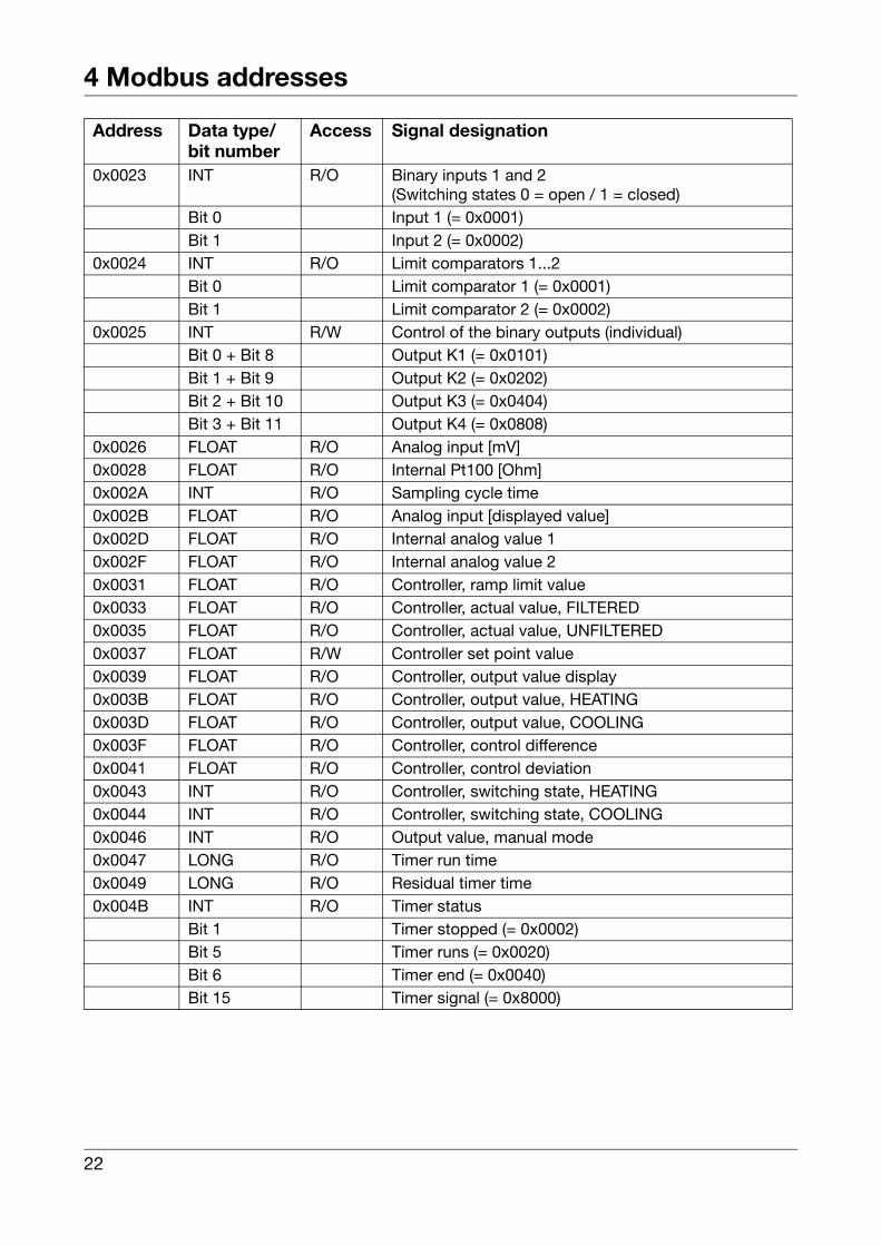
4 Modbus addresses
0x0023 INT R/O Binary inputs 1 and 2(Switching states 0 = open / 1 = closed)
Bit 0 Input 1 (= 0x0001)Bit 1 Input 2 (= 0x0002)
0x0024 INT R/O Limit comparators 1...2Bit 0 Limit comparator 1 (= 0x0001)Bit 1 Limit comparator 2 (= 0x0002)
0x0025 INT R/W Control of the binary outputs (individual)Bit 0 + Bit 8 Output K1 (= 0x0101)Bit 1 + Bit 9 Output K2 (= 0x0202)Bit 2 + Bit 10 Output K3 (= 0x0404)Bit 3 + Bit 11 Output K4 (= 0x0808)
0x0026 FLOAT R/O Analog input [mV]0x0028 FLOAT R/O Internal Pt100 [Ohm]0x002A INT R/O Sampling cycle time0x002B FLOAT R/O Analog input [displayed value]0x002D FLOAT R/O Internal analog value 10x002F FLOAT R/O Internal analog value 20x0031 FLOAT R/O Controller, ramp limit value0x0033 FLOAT R/O Controller, actual value, FILTERED0x0035 FLOAT R/O Controller, actual value, UNFILTERED0x0037 FLOAT R/W Controller set point value0x0039 FLOAT R/O Controller, output value display0x003B FLOAT R/O Controller, output value, HEATING0x003D FLOAT R/O Controller, output value, COOLING0x003F FLOAT R/O Controller, control difference0x0041 FLOAT R/O Controller, control deviation0x0043 INT R/O Controller, switching state, HEATING0x0044 INT R/O Controller, switching state, COOLING0x0046 INT R/O Output value, manual mode0x0047 LONG R/O Timer run time0x0049 LONG R/O Residual timer time0x004B INT R/O Timer status
Bit 1 Timer stopped (= 0x0002)Bit 5 Timer runs (= 0x0020)Bit 6 Timer end (= 0x0040)Bit 15 Timer signal (= 0x8000)
Address Data type/bit number
Access Signal designation
22
4 Modbus addresses
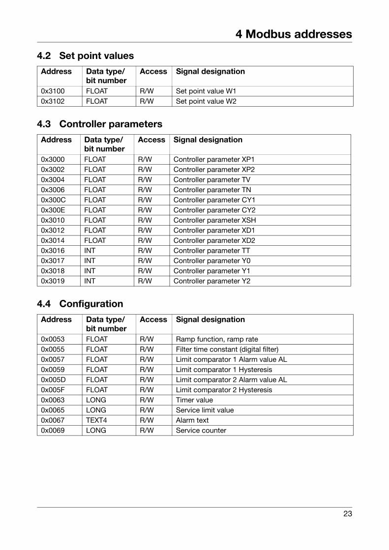
4.2 Set point values
4.3 Controller parameters
4.4 Configuration
Address Data type/bit number
Access Signal designation
0x3100 FLOAT R/W Set point value W10x3102 FLOAT R/W Set point value W2
Address Data type/bit number
Access Signal designation
0x3000 FLOAT R/W Controller parameter XP10x3002 FLOAT R/W Controller parameter XP20x3004 FLOAT R/W Controller parameter TV0x3006 FLOAT R/W Controller parameter TN0x300C FLOAT R/W Controller parameter CY10x300E FLOAT R/W Controller parameter CY20x3010 FLOAT R/W Controller parameter XSH0x3012 FLOAT R/W Controller parameter XD10x3014 FLOAT R/W Controller parameter XD20x3016 INT R/W Controller parameter TT0x3017 INT R/W Controller parameter Y00x3018 INT R/W Controller parameter Y10x3019 INT R/W Controller parameter Y2
Address Data type/bit number
Access Signal designation
0x0053 FLOAT R/W Ramp function, ramp rate0x0055 FLOAT R/W Filter time constant (digital filter)0x0057 FLOAT R/W Limit comparator 1 Alarm value AL0x0059 FLOAT R/W Limit comparator 1 Hysteresis0x005D FLOAT R/W Limit comparator 2 Alarm value AL0x005F FLOAT R/W Limit comparator 2 Hysteresis0x0063 LONG R/W Timer value0x0065 LONG R/W Service limit value0x0067 TEXT4 R/W Alarm text0x0069 LONG R/W Service counter
23

4 Modbus addresses
4.5 Commands
Address Data type/bit number
Access Signal designation
0x004D INT W/O Binary functions CONTROLLERBit 0 Self-optimization start (=0x0001)Bit 1 Self-optimization abort (=0x0002)Bit 2 Manual operation (= 0x0004)Bit 3 Automatic operation (= 0x0008)Bit 4 Controller off (= 0x0010)Bit 5 Manual mode inhibit (= 0x0020)Bit 6 Ramp stop (= 0x0040)Bit 7 Ramp abort (= 0x0080)Bit 8 Ramp restart (= 0x0100)Bit 9 Timer start (= 0x0200)Bit 10 Timer abort (= 0x0400)Bit 11 Timer stop (= 0x0800)
0x004E INT W/O Binary functions OPERATIONBit 0 Keyboard inhibit (= 0x0001)Bit 1 Configuration and parameter level inhibit
(= 0x0002)Bit 3 Display OFF (= 0x0008)Bit 5 Text display (= 0x0020)
0x004F INT W/O Binary functions TIMERBit 9 Timer start (= 0x0200)Bit 10 Timer abort (= 0x0400)Bit 11 Timer stop (= 0x0800)
0x0050 INT R/W Set point value togglingBit 0 Set point value 1 (= 0x0001)Bit 1 Set point value 2 (= 0x0002)
24

4 Modbus addresses
4.6 RAM memory
Address Data type/bit number
Access Signal designation
0x3200 FLOAT W/O Controller set point value (writable)0x3202 FLOAT W/O Controller actual value (writable)0x3204 FLOAT W/O Internal analog value 1 (writable)0x3206 FLOAT W/O Internal analog value 2 (writable)0x3208 INT W/O Internal binary values (writable)
Bit 0 + Bit 7 Binary value L1 (= 0x0081)Bit 1 + Bit 7 Binary value L2 (= 0x0082)
H Modbus allows direct access to the RAM memory of the controller for writing thecontroller set point value (0x3200), the controller actual value (0x3202) and the internalanalog values (0x3204, 0x3206) as well as the internal binary values (0x3208).
When writing, a range between -1999 and +9999 is available for the controller set pointvalues, controller actual values and the internal analog values. In this case, the datawritten in the controller is used instead of the original value.
If you wish to use the original value again on the controller, write the value 200001 at thememory location concerned via Modbus.
25

4 Modbus addresses
26


JUMO GmbH & Co. KG JUMO Instrument Co. Ltd. JUMO Process Control, Inc.Street address:Moritz-Juchheim-Straße 136039 Fulda, GermanyDelivery address:Mackenrodtstraße 1436039 Fulda, GermanyPostal address:36035 Fulda, GermanyPhone: +49 661 6003-0Fax: +49 661 6003-607e-mail: [email protected]: www.jumo.net
JUMO HouseTemple Bank, RiverwayHarlow, Essex CM 20 2 TT, UKPhone: +44 1279 635533Fax: +44 1279 635262e-mail: [email protected]: www.jumo.co.uk
8 Technology BoulevardCanastota, NY 13032, USAPhone: 315-697-JUMO
1-800-554-JUMOFax: 315-697-5867e-mail: [email protected]: www.jumo.us