CMC Smart Rack July Aug 2010 Metal Tech Speaking Template ...
6
New Technology for Electroplating Metal Layers Aims to Improve Thickness Control C MC Laboratories has developed a new technology for electroplating metal layers that results in sig- nificant improvements in thickness control. 1 CMC’s technology, which is called “Smart Rack,” utilizes active control of the plating process to improve thickness ver- sus traditional passive controls such as current thieves. CMC’s Smart Rack technology entails a new electro- plating circuit as well as a completely different approach to rack design. Though this technology was developed for electronic devices or package applica- tions, it can easily be applied in other areas that utilize precious metal plating. The focus of this new technology is to narrow the dis- tribution of plated layer thicknesses across a plating rack. Narrowing this distribution can have a significant impact on precious metal plated layers, such as Au, Pt, Pd, Rh, and Ir. When a minimum thickness of these expensive metals is specified, as is typical, a narrower distribution results in less metal used for significant cost savings. A tighter plating distribution can also be important for other metal plating processes. For example, currently most wafer bump plating is done using low throughput, high tool cost fountain platers. For small wafer size (< 6 inches), it may be possible to use Smart Rack technology to bump multiple wafers at one time in a rack configura- tion. Since Smart Rack only improves part to part thick- ness control, not the thickness distri- bution across a part, the technology would not help for very large wafers. The ability to plate AuSn at the eutectic composition on die attach pads would also be very important in many high power electronic applications. However, since the composition of AuSn varies with current density, it is very TECHNICALLY speaking BY G. CARRASCO, DR. J. HARRIS, T. BECKETT, AND E. RUBEL, CMC LABORATORIES, TEMPE, ARIZ. difficult to achieve the 80/20 eutectic across a large plat- ing rack. AuSn compositions that are off eutectic will not melt at the 400C process temperature. 2 Traditional electrolytic plating uses a plating rack that is made of a highly conductive metal such as cop- per or stainless steel. All of the parts being plated are attached to this rack. During the plating process, the rack is attached to a constant current power supply (plating rectifier). Current is pumped through the rack structure, forcing the plating reaction to occur at the interface between the conducting work parts and the plating solution or electrolyte. The plating rate at each individual part depends on a number of factors: • The electrical current density at the individual part • The availability of metal ions in solution at the location of the individual part • The availability of other electrochemical reactants at the plating interface which compete with the plating reaction Macroscopic factors that affect these more microscopic reactions include: • Density of plating parts surrounding the individual, part being plated • Resistance drops across the plating rack • Location of the part on the rack • Plating rate • Uniformity of the electrochemical environment including variations in solution chemistry, temperature, agitation All of these variations lead to thickness varia- tion in parts from one location of a plating rack to the next. xx I metalfinishing I July/August 2010 www.metalfinishing.com Figure 1a. Electrically isolated rack pieces. Figure 1b CMC Smart Rack July Aug 2010:Metal Tech Speaking Template USE THIS.qxd 7/19/2010 2:20 PM Page 1
Transcript of CMC Smart Rack July Aug 2010 Metal Tech Speaking Template ...

New Technology forElectroplating Metal
Layers Aims to ImproveThickness Control
CMC Laboratories has developed a new technologyfor electroplating metal layers that results in sig-
nificant improvements in thickness control.1 CMC’stechnology, which is called “Smart Rack,” utilizes activecontrol of the plating process to improve thickness ver-sus traditional passive controls such as current thieves.CMC’s Smart Rack technology entails a new electro-plating circuit as well as a completely differentapproach to rack design. Though this technology wasdeveloped for electronic devices or package applica-tions, it can easily be applied in other areas that utilizeprecious metal plating.The focus of this new technology is to narrow the dis-
tribution of plated layer thicknesses across a plating rack.Narrowing this distribution can have a significant impacton precious metal plated layers, such as Au, Pt, Pd, Rh,and Ir. When a minimum thickness of these expensivemetals is specified, as is typical, a narrower distributionresults in less metal used for significant cost savings. A tighter plating distribution can also be important for
other metal plating processes. For example, currentlymost wafer bump plating is done using low throughput,high tool cost fountain platers. For small wafer size (< 6inches), it may be possible to use Smart Rack technologyto bump multiplewafers at one timein a rack configura-tion. Since SmartRack only improvespart to part thick-ness control, notthe thickness distri-bution across apart, the technology would not help for very large wafers.The ability to plate AuSn at the eutectic composition on
die attach pads would also be very important in manyhigh power electronic applications. However, since thecomposition of AuSn varies with current density, it is very
TECHNICALLYspeaking
BY G. CARRASCO, DR. J. HARRIS, T. BECKETT, AND E.
RUBEL, CMC LABORATORIES, TEMPE, ARIZ.
difficult to achieve the 80/20 eutectic across a large plat-ing rack. AuSn compositions that are off eutectic will notmelt at the 400C process temperature.2
Traditional electrolytic plating uses a plating rackthat is made of a highly conductive metal such as cop-per or stainless steel. All of the parts being plated areattached to this rack. During the plating process, therack is attached to a constant current power supply(plating rectifier). Current is pumped through the rackstructure, forcing the plating reaction to occur at theinterface between the conducting work parts and theplating solution or electrolyte. The plating rate at each individual part depends on a
number of factors:
• The electrical current density at the individual part• The availability of metal ions in solution at the location of the individual part
• The availability of other electrochemical reactants at the plating interface which compete with the plating reaction
Macroscopic factors that affect these more microscopicreactions include:
• Density of plating parts surrounding the individual, part being plated
• Resistance drops across the plating rack• Location of the part on the rack• Plating rate• Uniformity of the electrochemical environment including variations in solution chemistry, temperature, agitation
All of these variationslead to thickness varia-tion in parts from onelocation of a platingrack to the next.
xx I metalfinishing I July/August 2010 www.metalfinishing.com
Figure 1a. Electrically isolated rack pieces.
Figure 1b
CMC Smart Rack July Aug 2010:Metal Tech Speaking Template USE THIS.qxd 7/19/2010 2:20 PM Page 1
www.metalfinishing.com July/August 2010 I metalfinishing I xx
Typically the thickestparts are locatedalong the edge of therack and the thinnestparts are located nearthe center. One rea-son for this trend isthat the flow ofmetal ions to be plat-ed is unimpeded nearthe edge of the rack,but near the center ofthe rack, surround-ing parts “screen” themetal ion flow fromtheir neighboringparts. This competi-tion for plating ions
results in a thinner deposited layer and a lower platingcurrent density.
DESCRIPTION OF SMART RACK CONCEPTThe essential feature of the Smart Rack concept is to indi-vidually control the electrical current that flows to eachpiece during the plating process. This individual currentcontrol allows active and direct control of the platingprocess, which can very significantly narrow the platingthickness distribution. This direct method is much moreeffective than indirect methods such as current thieves,and the range of adjustment is considerably higher. Forexample, if desired, the programmed current density oftwo parts on the same rack could vary by factors of 2 ormore. In addition, this method is much easier to imple-ment and control because changes in current densitiescan be effected by adjusting inputs to the plating pro-gram rather than making any physical changes to theplating bath or set up.To accomplish this requires two significant changes
compared to the traditional plating approach. First, theplating rack must be constructed so that individual elec-trical current conductors are connected to each individ-ual piece on the rack, and thus each piece is electricallyisolated from all of the other pieces. The rack, rather thanbeing a large conductor, is now an insulator with individ-ual wires or embedded metal traces, to each piece. This isshown in the diagram in Figure 1. In this Figure, you cansee the cut out area where 2 parts are located and thetraces to each part from the top contact array shows inthe detail drawing.One option for fabricating this type of rack is to utilize
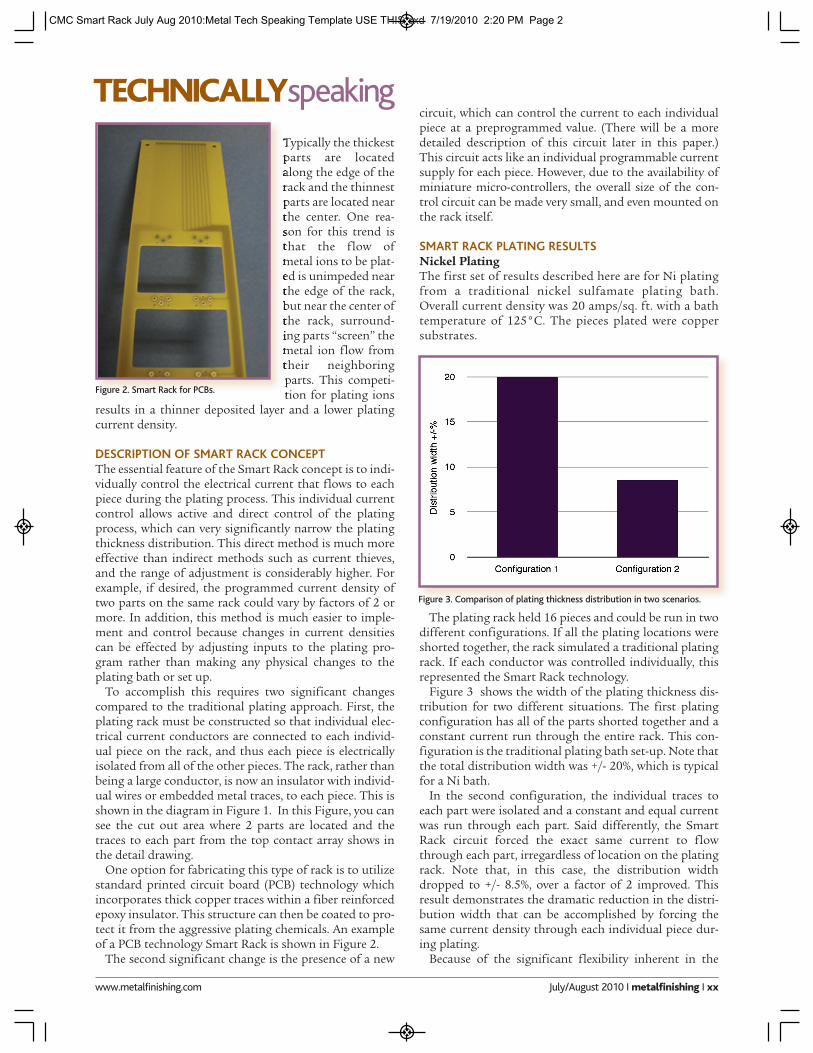
standard printed circuit board (PCB) technology whichincorporates thick copper traces within a fiber reinforcedepoxy insulator. This structure can then be coated to pro-tect it from the aggressive plating chemicals. An exampleof a PCB technology Smart Rack is shown in Figure 2. The second significant change is the presence of a new
TECHNICALLYspeakingcircuit, which can control the current to each individualpiece at a preprogrammed value. (There will be a moredetailed description of this circuit later in this paper.)This circuit acts like an individual programmable currentsupply for each piece. However, due to the availability ofminiature micro-controllers, the overall size of the con-trol circuit can be made very small, and even mounted onthe rack itself.
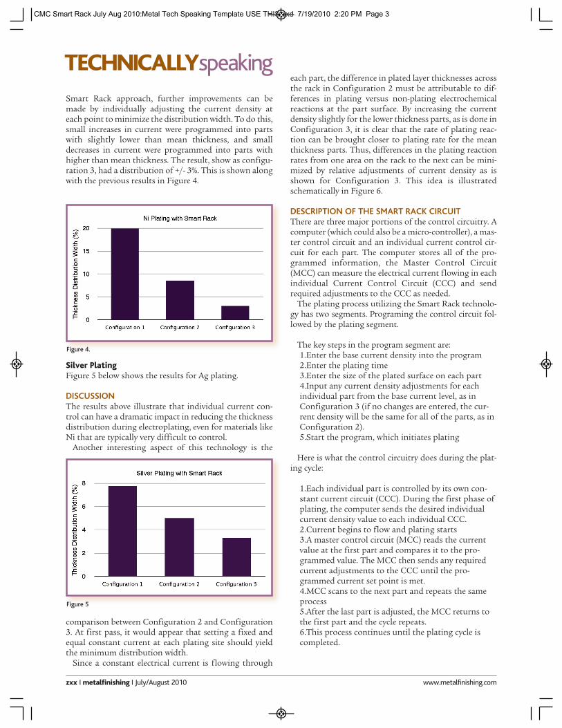
SMART RACK PLATING RESULTSNickel PlatingThe first set of results described here are for Ni platingfrom a traditional nickel sulfamate plating bath.Overall current density was 20 amps/sq. ft. with a bathtemperature of 125°C. The pieces plated were coppersubstrates.
The plating rack held 16 pieces and could be run in twodifferent configurations. If all the plating locations wereshorted together, the rack simulated a traditional platingrack. If each conductor was controlled individually, thisrepresented the Smart Rack technology.Figure 3 shows the width of the plating thickness dis-
tribution for two different situations. The first platingconfiguration has all of the parts shorted together and aconstant current run through the entire rack. This con-figuration is the traditional plating bath set-up. Note thatthe total distribution width was +/- 20%, which is typicalfor a Ni bath. In the second configuration, the individual traces to
each part were isolated and a constant and equal currentwas run through each part. Said differently, the SmartRack circuit forced the exact same current to flowthrough each part, irregardless of location on the platingrack. Note that, in this case, the distribution widthdropped to +/- 8.5%, over a factor of 2 improved. Thisresult demonstrates the dramatic reduction in the distri-bution width that can be accomplished by forcing thesame current density through each individual piece dur-ing plating.Because of the significant flexibility inherent in the
Figure 2. Smart Rack for PCBs.
Figure 3. Comparison of plating thickness distribution in two scenarios.
CMC Smart Rack July Aug 2010:Metal Tech Speaking Template USE THIS.qxd 7/19/2010 2:20 PM Page 2
Smart Rack approach, further improvements can bemade by individually adjusting the current density ateach point to minimize the distribution width. To do this,small increases in current were programmed into partswith slightly lower than mean thickness, and smalldecreases in current were programmed into parts withhigher than mean thickness. The result, show as configu-ration 3, had a distribution of +/- 3%. This is shown alongwith the previous results in Figure 4.
Silver PlatingFigure 5 below shows the results for Ag plating.
DISCUSSIONThe results above illustrate that individual current con-trol can have a dramatic impact in reducing the thicknessdistribution during electroplating, even for materials likeNi that are typically very difficult to control.Another interesting aspect of this technology is the
comparison between Configuration 2 and Configuration3. At first pass, it would appear that setting a fixed andequal constant current at each plating site should yieldthe minimum distribution width. Since a constant electrical current is flowing through
TECHNICALLYspeakingeach part, the difference in plated layer thicknesses acrossthe rack in Configuration 2 must be attributable to dif-ferences in plating versus non-plating electrochemicalreactions at the part surface. By increasing the currentdensity slightly for the lower thickness parts, as is done inConfiguration 3, it is clear that the rate of plating reac-tion can be brought closer to plating rate for the meanthickness parts. Thus, differences in the plating reactionrates from one area on the rack to the next can be mini-mized by relative adjustments of current density as isshown for Configuration 3. This idea is illustratedschematically in Figure 6.
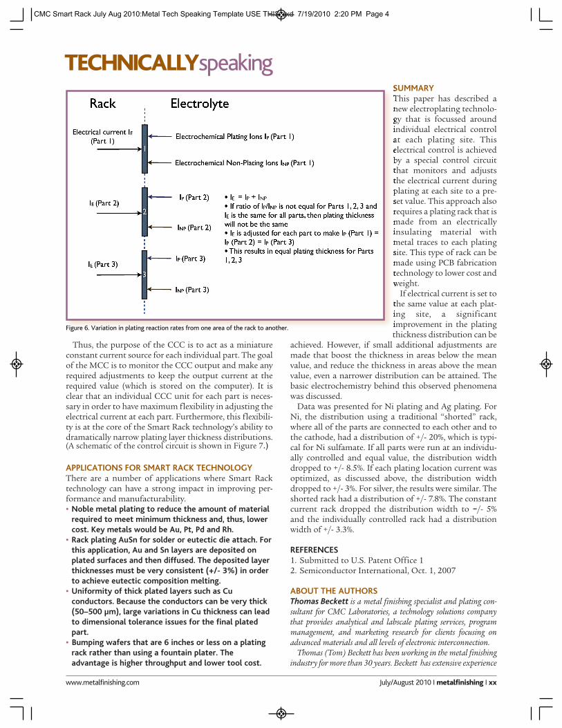
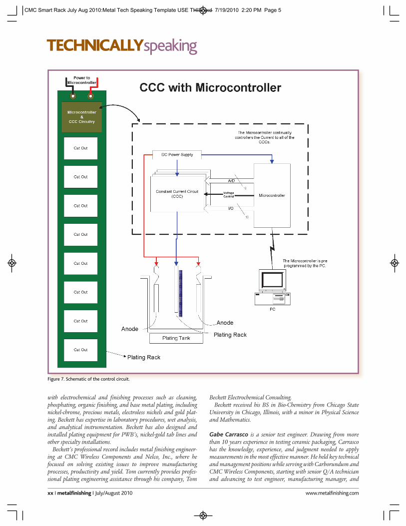
DESCRIPTION OF THE SMART RACK CIRCUITThere are three major portions of the control circuitry. Acomputer (which could also be a micro-controller), a mas-ter control circuit and an individual current control cir-cuit for each part. The computer stores all of the pro-grammed information, the Master Control Circuit(MCC) can measure the electrical current flowing in eachindividual Current Control Circuit (CCC) and sendrequired adjustments to the CCC as needed.The plating process utilizing the Smart Rack technolo-
gy has two segments. Programing the control circuit fol-lowed by the plating segment.
The key steps in the program segment are:1.Enter the base current density into the program2.Enter the plating time3.Enter the size of the plated surface on each part4.Input any current density adjustments for eachindividual part from the base current level, as inConfiguration 3 (if no changes are entered, the cur-rent density will be the same for all of the parts, as inConfiguration 2).5.Start the program, which initiates plating
Here is what the control circuitry does during the plat-ing cycle:
1.Each individual part is controlled by its own con-stant current circuit (CCC). During the first phase ofplating, the computer sends the desired individualcurrent density value to each individual CCC.2.Current begins to flow and plating starts3.A master control circuit (MCC) reads the currentvalue at the first part and compares it to the pro-grammed value. The MCC then sends any requiredcurrent adjustments to the CCC until the pro-grammed current set point is met.4.MCC scans to the next part and repeats the sameprocess5.After the last part is adjusted, the MCC returns tothe first part and the cycle repeats.6.This process continues until the plating cycle iscompleted.
zxx I metalfinishing I July/August 2010 www.metalfinishing.com
Figure 4.
Figure 5
CMC Smart Rack July Aug 2010:Metal Tech Speaking Template USE THIS.qxd 7/19/2010 2:20 PM Page 3
www.metalfinishing.com July/August 2010 I metalfinishing I xx
Thus, the purpose of the CCC is to act as a miniatureconstant current source for each individual part. The goalof the MCC is to monitor the CCC output and make anyrequired adjustments to keep the output current at therequired value (which is stored on the computer). It isclear that an individual CCC unit for each part is neces-sary in order to have maximum flexibility in adjusting theelectrical current at each part. Furthermore, this flexibili-ty is at the core of the Smart Rack technology’s ability todramatically narrow plating layer thickness distributions.(A schematic of the control circuit is shown in Figure 7.)
APPLICATIONS FOR SMART RACK TECHNOLOGYThere are a number of applications where Smart Racktechnology can have a strong impact in improving per-formance and manufacturability.• Noble metal plating to reduce the amount of material required to meet minimum thickness and, thus, lower cost. Key metals would be Au, Pt, Pd and Rh.
• Rack plating AuSn for solder or eutectic die attach. Forthis application, Au and Sn layers are deposited on plated surfaces and then diffused. The deposited layer thicknesses must be very consistent (+/- 3%) in order to achieve eutectic composition melting.
• Uniformity of thick plated layers such as Cu conductors. Because the conductors can be very thick (50–500 µm), large variations in Cu thickness can lead to dimensional tolerance issues for the final plated part.
• Bumping wafers that are 6 inches or less on a plating rack rather than using a fountain plater. The advantage is higher throughput and lower tool cost.
TECHNICALLYspeakingSUMMARYThis paper has described anew electroplating technolo-gy that is focussed aroundindividual electrical controlat each plating site. Thiselectrical control is achievedby a special control circuitthat monitors and adjuststhe electrical current duringplating at each site to a pre-set value. This approach alsorequires a plating rack that ismade from an electricallyinsulating material withmetal traces to each platingsite. This type of rack can bemade using PCB fabricationtechnology to lower cost andweight.If electrical current is set to
the same value at each plat-ing site, a significantimprovement in the platingthickness distribution can be
achieved. However, if small additional adjustments aremade that boost the thickness in areas below the meanvalue, and reduce the thickness in areas above the meanvalue, even a narrower distribution can be attained. Thebasic electrochemistry behind this observed phenomenawas discussed. Data was presented for Ni plating and Ag plating. For
Ni, the distribution using a traditional “shorted” rack,where all of the parts are connected to each other and tothe cathode, had a distribution of +/- 20%, which is typi-cal for Ni sulfamate. If all parts were run at an individu-ally controlled and equal value, the distribution widthdropped to +/- 8.5%. If each plating location current wasoptimized, as discussed above, the distribution widthdropped to +/- 3%. For silver, the results were similar. Theshorted rack had a distribution of +/- 7.8%. The constantcurrent rack dropped the distribution width to =/- 5%and the individually controlled rack had a distributionwidth of +/- 3.3%.
REFERENCES1. Submitted to U.S. Patent Office 1 2. Semiconductor International, Oct. 1, 2007
ABOUT THE AUTHORS Thomas Beckett is a metal finishing specialist and plating con-sultant for CMC Laboratories, a technology solutions companythat provides analytical and labscale plating services, programmanagement, and marketing research for clients focusing onadvanced materials and all levels of electronic interconnection. Thomas (Tom) Beckett has been working in the metal finishing
industry for more than 30 years. Beckett has extensive experience
Figure 6. Variation in plating reaction rates from one area of the rack to another.
CMC Smart Rack July Aug 2010:Metal Tech Speaking Template USE THIS.qxd 7/19/2010 2:20 PM Page 4
with electrochemical and finishing processes such as cleaning,phosphating, organic finishing, and base metal plating, includingnickel-chrome, precious metals, electroless nickels and gold plat-ing. Beckett has expertise in laboratory procedures, wet analysis,and analytical instrumentation. Beckett has also designed andinstalled plating equipment for PWB’s, nickel-gold tab lines andother specialty installations.Beckett’s professional record includes metal finishing engineer-
ing at CMC Wireless Components and Nelco, Inc., where hefocused on solving existing issues to improve manufacturingprocesses, productivity and yield. Tom currently provides profes-sional plating engineering assistance through his company, Tom
TECHNICALLYspeaking
Beckett Electrochemical Consulting. Beckett received his BS in Bio-Chemistry from Chicago State
University in Chicago, Illinois, with a minor in Physical Scienceand Mathematics.
Gabe Carrasco is a senior test engineer. Drawing from morethan 10 years experience in testing ceramic packaging, Carrascohas the knowledge, experience, and judgment needed to applymeasurements in the most effective manner. He held key technicaland management positions while serving with Carborundum andCMC Wireless Components, starting with senior Q/A technicianand advancing to test engineer, manufacturing manager, and
xx I metalfinishing I July/August 2010 www.metalfinishing.com
Figure 7. Schematic of the control circuit.
CMC Smart Rack July Aug 2010:Metal Tech Speaking Template USE THIS.qxd 7/19/2010 2:20 PM Page 5

www.metalfinishing.com July/August 2010 I metalfinishing I xx
then vice president of operations. For CMC Laboratories,Carrasco serves as the Sr. Test Engineer overseeing theEnvironmental, Thermal and RF/Electrical testing.
Dr. J. Harris has played a leadership role in the advanced ceram-ic materials and electronic packaging industry over the past 20years. Dr. Harris is currently the President of CMC Laboratories,Inc., a materials analysis and consulting firm that focuses onadvanced materials used in electronic applications. CMC providesa range of technology services, including materials related con-sulting, materials characterization, analytical services, prototypefabrication, and technology licensing. Dr. Harris received his doc-torate in Solid State Physics from Brown University (Providence,RI) in 1983. He is the author of more than 50 publications andbook chapters and has 20 US Patents.
Erich Rubel is director, analytical services. He has more than 20years of experience working in quality, R&D, and failure analy-sis laboratories serving both the electronics and aerospace indus-try. His educational and technical focus spans the fields of chem-istry, metallurgy, and materials science. Rubel gained extensivefamiliarity with advanced materials and processes while workingat Honeywell, Inc. and later at CMC Wireless Components. Hecurrently manages the SEM and Metallurgical Laboratories atCMC Laboratories.
REFERENCES 1.Submitted to U.S. Patent Office12.Semiconductor International, Oct. 1, 2007
TECHNICALLYspeaking
CMC Smart Rack July Aug 2010:Metal Tech Speaking Template USE THIS.qxd 7/19/2010 2:20 PM Page 6