CMC Conference - ASM Wilk Final (Read-Only) - TECHCET...2018/05/16 · |$4...
21
ALD MATERIALS INTEGRATION CHALLENGES GLEN WILK
Transcript of CMC Conference - ASM Wilk Final (Read-Only) - TECHCET...2018/05/16 · |$4...

ALD MATERIALS INTEGRATION CHALLENGES
GLEN WILK

| 2
OUTLINE
› Industry Trends for Materials and Architectures
› Examples of materials innovations• High-k and metal gate
• Patterning materials
• New spacer materials
• Low thermal budget processes
› Needs from Chemical Suppliers

| 3
INDUSTRY TRENDS

| 4
ARCHITECTURAL INNOVATIONS: MOORE’S LAW ENABLERS
Planar FG NAND
Charge trap NAND
Bipolar
Planar CMOS
Stacked capacitor
FinFET
TSV’s
Planar DRAM
3D NAND
Cross-point
Dual Damascene
Multilevel interconnect
Spacer Defined Patterning
Airgaps
e-DRAM
e-RRAM
Pillar capacitor
SoC
H-nanowires
V-nanowires
TFET
Self-aligned via’sSOI
Stacked CMOS
Hetero-semi stacksSTT RAMTrench
capacitor
RCAT
~1980 ~2000 ~2020
Buried WL
Cylinder capacitor
FDSOI

| 5
INDUSTRY TRENDS IN LOGIC
Higher Capacitance, Lower Leakage Higher Mobility, Lower Resistance
Smaller Feature SizesLess Cross Talk, Faster Interconnect
(Porous) Low-k Materials
Improved Metals
High-k and Metal Gates
DRAM, RF, decoupling capacitors
Strain and new Channel MaterialsNew metal contacts
-EUV delays led to more double patterning (SDDP/SDQP) -EUV will enable many new materials
ASM Proprietary and Confidential Information
© Chipworks
| 6
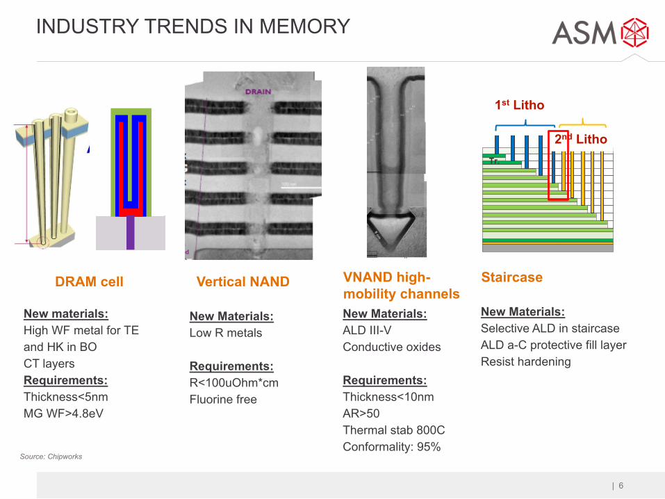
INDUSTRY TRENDS IN MEMORY
VNAND high-mobility channels
Vertical NANDDRAM cell Staircase
New Materials:ALD III-VConductive oxides
Requirements:Thickness<10nmAR>50Thermal stab 800CConformality: 95%
New Materials:Low R metals
Requirements:R<100uOhm*cmFluorine free
New materials:High WF metal for TE and HK in BOCT layersRequirements: Thickness<5nmMG WF>4.8eV
New Materials:Selective ALD in staircaseALD a-C protective fill layerResist hardening
1st Litho
Sel. Tr.
.
Sel. Tr.
2nd Litho
Source: Chipworks

| 7
MATERIALS INNOVATIONS

| 8
NEW MATERIALS: MOORE’S LAW ENABLERS
sSOI/GeOIGe ILIII-‐V IL
* GaNInSb
InGaAsGeSTORu
Other PM'sEUV
Other PM'sEUV
Co CoSi(C)P Si(C)PFDSOI FDSOISiC SiCAir AirSiCO SiCOLaO LaOLT SiO LT SiO
SiCN SiCN SiCNTiAlC MG TiAlC MG TiAlC MG
ZrO ZrO ZrOHf(Si)O Hf(Si)O Hf(Si)OAlO AlO AlOpSiOC pSiOC pSiOCSOI SOI SOI
SiGe(B) SiGe(B) SiGe(B)TaO TaO TaO TaOSOG SOG SOG SOGSiOC SiOC SiOC SiOC
Ta/TaN Ta/TaN Ta/TaN Ta/TaNCu Cu Cu CuSiOF SiOF SiOF SiOF
TiSi TiSi TiSi TiSi TiSiPtSi PtSi PtSi PtSi PtSi
TiW TiW TiW/TiN TiN TiN TiNWSi, MoSi WSi, W WSi, W W W W
BPSG BPSG BPSG BPSG BPSG BPSG BPSGAl Al Al Al Al Al Al Al
SiO, SiN SiO, SiN SiO, SiN SiO, SiN SiO, SiN SiO, SiN SiO, SiN SiO, SiNSi Si Si Si Si Si Si Si
1960 1970 1980 1990 2000 2010 2015 2020(*)
(*): Projection
Patterning RelatedBEOLFEOLStarting Materials

| 9
THERMAL ALD SOLUTIONS CRITICAL FOR 3D STRUCTURES
› Move to 3D devices necessitates the use of pure thermal ALD techniques
› Lower thermal budgets for ALD and PEALD
Thermal ALD Plasma ALD
Directional nature of reactants results in non-uniform composition
Step coverage limited (especially in re-entrant structures)
Near perfect step coverage in deep and re-entrant structures
Stoichiometric film regardless of directionality
Source: SemiEngineering
Source: IMEC

| 10
PROCESS INNOVATIONS: MOORE’S LAW ENABLERS
› Thermal and plasma-enhanced ALD are materials enablers: l High-k capacitor
l High-k gate dielectric
l Metal gate
l Metal Nitrides (HfN)
l Low-T oxide
l Low-T nitride… Made by ASM

| 11
PROCESS INNOVATIONS: ALD AND PEALD
› Atomic Layer Deposition separates reactive precursors in time (or space), and grows materials one ‘atomic’ layer at a timel Superb control of uniformity, conformality, quality, and composition over any topography
l Plasma Enhanced ALD provides high quality materials at lower temperatures
l Need many etch selective materials with wide range of film properties and compositions
› ALD and PEALD are architecture enablers: High Aspect Ratio structures, FinFET, double patterning, VNAND,…
Right: NY Times 2011;; http://electroiq.com/chipworks_real_chips_blog/2014/08/04/

| 12
METAL FOR VNAND WL FOR VERTICAL & LATERAL PITCH SCALING
› To enable vertical scaling of word linel Development of ALD TiN with fast-closing layer < 15A
l Development of F-free ALD processes
l New precursors

| 13
CRITICAL ALD SUPPLY CHAIN COMPONENTS
Fundamental Capability
Process Performance Productivity Integrated
ProcessFinal Product Capability
Precursors
Precursor Delivery, Valves and Vessels
Reactors
Fab facilities,pumps & abatement
High productivity tools

| 14
WHAT’S NEXT IN PROCESS INNOVATIONS?
› The surface sensitivity of ALD and CVD may be ideal to create selective deposition l Many potential applications exist in memory, logic, interconnect, and patterningl Building templated self-aligned structures: reduction of overlay requirements
› Strong need for many variations of selective ALD: Metal on Metal, Dielectric on Dielectric, etc.› Reversing the reaction to highly selective Atomic Layer Etching
Si
H H H H H H
Cu
OH O OH OHO O
Cu
CH3
Restored Low-k
O CH3 CH3 OCH3
OH O OH OH O
Damaged low-k
OH
Si
OH OH OH OH OH OHNat. Oxide
Si3N4
NH2 NH NH2 NH2N NH
TiN
NH2 NH OH NH2N N
SiO2
O O OOHOH OH

| 15
LOW THERMAL BUDGET PROCESSES

| 16
HIGH MOBILITY CHANNEL MATERIALS
› Voltage scaling requires high mobility channel materials with proper bandgap› Introduction will probably be simultaneous with architecture change to nanowires› Epitaxy and ALD will be enabling deposition technologies
2011
~2021
| 17
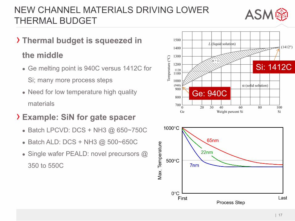
NEW CHANNEL MATERIALS DRIVING LOWER THERMAL BUDGET
› Thermal budget is squeezed in the middlel Ge melting point is 940C versus 1412C for
Si;; many more process steps
l Need for low temperature high quality
materials
› Example: SiN for gate spacerl Batch LPCVD: DCS + NH3 @ 650~750C
l Batch ALD: DCS + NH3 @ 500~650C
l Single wafer PEALD: novel precursors @
350 to 550C
Si: 1412C
Ge: 940C

| 18
NEEDS FROM CHEMICAL SUPPLIERS

| 19
HOW CHEMICAL SUPPLIERS CAN HELP
› Novel materialsl Precursors for low-resistivity metals, ternary films with incorporation from the precursor
as part of deposition process
l Highly reactive precursors that can enable fast film closure
› Precursors with high reactivity at low temperaturel New materials are driving FEOL processes toward 400C
l Enabling low-T processes for existing materials like SiO and SiN
› Chemicals that do not easily decompose even with long residence times in reactors for high-aspect ratio structuresl Solid precursors, lower-volatility liquids
› Enable faster development cycle by doing more in-house pre-screeningl Representative reactors and structures to show upfront feasibility for step coverage,
utilization, efficiency of incorporation

| 20
CONCLUSION AND SUMMARY
›Moore’s Law is increasingly a materials playl Enabling materials such as HfO2, ZrO2, Si:Ge, Si:P, Co, …
l Enabling processes for existing materials like LT SiO and SiN
› New device architectures and EUV will drive stronger need for flexible chemistries and film properties
› Selective deposition in various combinations of surface and film type will be required
›Many opportunities for enabling materials solutions with innovative chemistries

| 21
ACKNOWLEDGEMENTS
Thanks for your attention!
›Thanks to Ivo Raaijmakers, Bob Hollands, Bert Jongbloed, Jan Willem Maes, John Cossins, Hessel Sprey, and many others for providing material, and their help in preparing, for this presentation