Circuit Techniques for Mitigating Short-Term Vth...
22
Circuit Techniques for Mitigating Short-Term Vth Instability Issues in SAR ADCs Won Ho Choi, Hoonki Kim, and Chris H. Kim University of Minnesota, Minneapolis, MN [email protected]
Transcript of Circuit Techniques for Mitigating Short-Term Vth...
Circuit Techniques for Mitigating Short-Term Vth Instability Issues
in SAR ADCs
Won Ho Choi, Hoonki Kim, and Chris H. Kim
University of Minnesota, Minneapolis, MN
2/22
Agenda
• Impact of Short-term Vth Instability on SAR ADC Operation
• Proposed Stress Mitigation Techniques
• SAR ADC Test-chip Measurement Results
• Conclusions

3/22
Intro to Bias Temperature Instability (BTI)
• Channel carriers interact with interface bonds and get captured in dielectric or interface
• Manifests as increase in |Vth| with time
• Partially recovers when FET is turned off
p+ p+
Gate dielectric
p+ p+
Stress (on-state) Recovery (off-state)
VDD
VDDVDDVDD
+ ++
++ +

4/22
Short-term Vth Instability due to BTI
• Short-term Vth degradation and recovery occur due to the BTI
• The amount of Vth shift depends on the stress voltage and stress time
J. Keane, et al., JSSC, 2011.

5/22
Impact on Comparator Circuit
• Asymmetric input voltage ���� asymmetric time-dependent Vth shift between input transistors ���� time-dependantinput offset
VIP VIN
VOUT
Stress-induced input offset
~5mV ∆Vth difference
K. Rott, et al., IIRW, 2012.
6/22
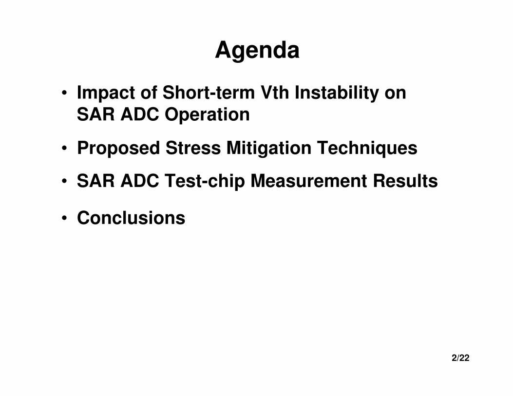
Case Study: 10-bit SAR ADC
• Stress-induced input offset of the comparator may degrade the resolution of a Successive Approximation Register (SAR) ADC
VREF
VIN-
VCM
VIN+
VREF
Comparator
SAR Controller
D0 ~ D9
10b
CLK
512C
256C
128
C
64C
32C
16C
8C
4C
2C
1C
1C
C_CLK
512C
256C
128
C
64C
32C
16C
8C
4C
2C
1C
1C
VIP
VIN
7/22
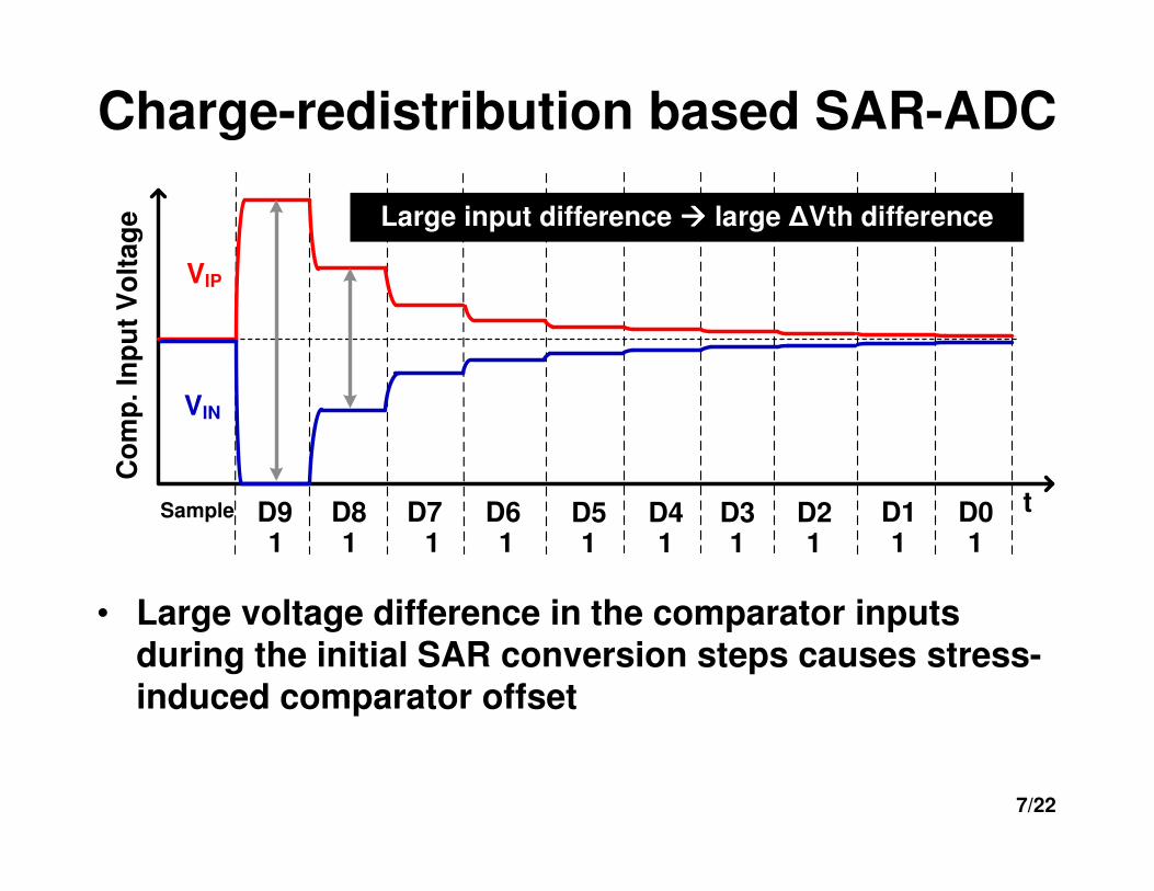
Charge-redistribution based SAR-ADC
• Large voltage difference in the comparator inputs during the initial SAR conversion steps causes stress-induced comparator offset
1 1 1 1 1 1
VIP
VIN
D9 D8 D7 D6 D1 D0 t
Co
mp
. In
pu
t V
olt
ag
e
1 1D3 D2
1 1D5 D4Sample
Large input difference ���� large ΔVth difference
8/22
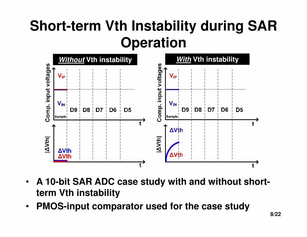
Short-term Vth Instability during SAR Operation
• A 10-bit SAR ADC case study with and without short-term Vth instability
• PMOS-input comparator used for the case study
Without Vth instability With Vth instability

9/22
Short-term Vth Instability during SAR Operation
• A large input voltage difference gives rise to a large difference in short-term Vth shifts
Without Vth instability With Vth instability
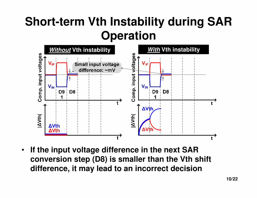
10/22
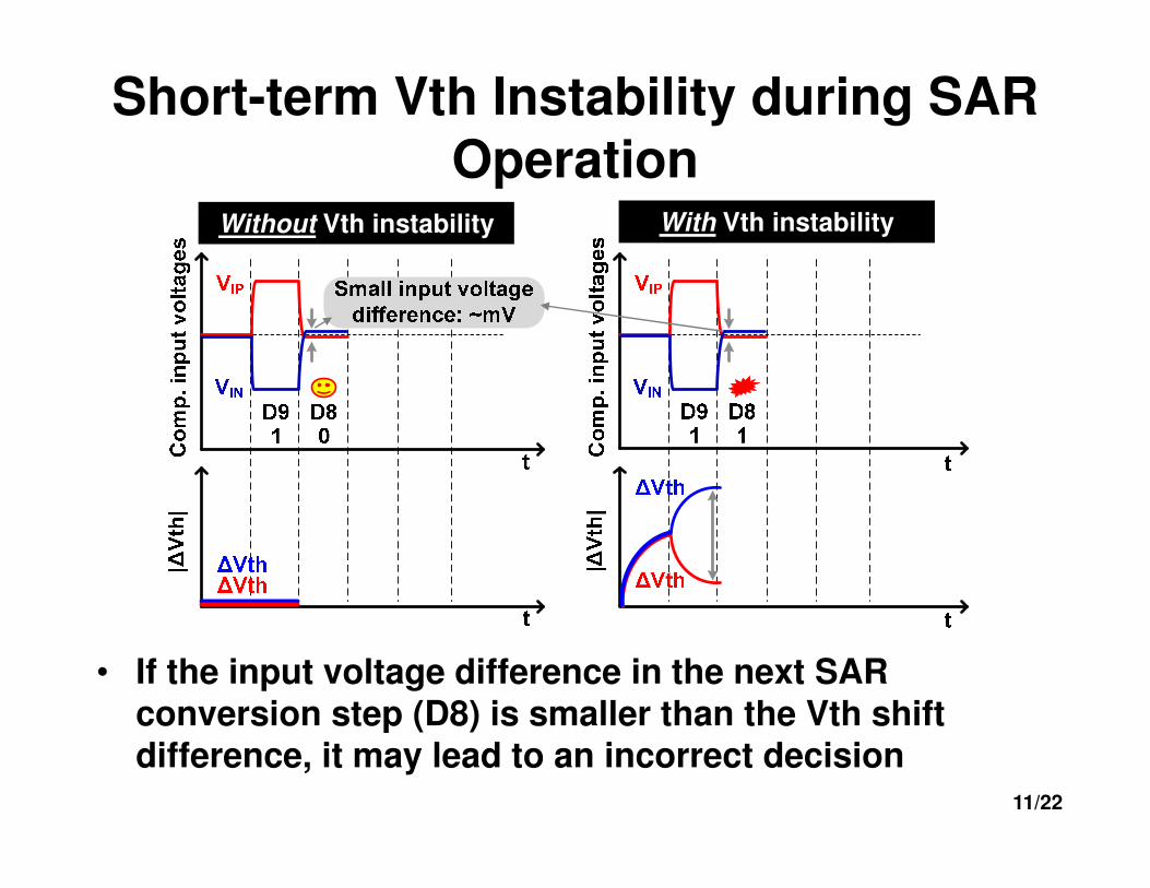
Short-term Vth Instability during SAR Operation
Without Vth instability With Vth instability
• If the input voltage difference in the next SAR conversion step (D8) is smaller than the Vth shift difference, it may lead to an incorrect decision
11/22
Short-term Vth Instability during SAR Operation
Without Vth instability With Vth instability
• If the input voltage difference in the next SAR conversion step (D8) is smaller than the Vth shift difference, it may lead to an incorrect decision

12/22
Short-term Vth Instability during SAR Operation
• The error cannot be corrected by the subsequent conversion steps (…0111 vs. …1000)
• An error of one LSB generated in the digital output
Without Vth instability With Vth instability
13/22
Agenda
• Impact of Short-term Vth Instability on SAR ADC operation
• Proposed Stress Mitigation Techniques
• SAR ADC Test-chip Measurement Results
• Conclusions

14/22
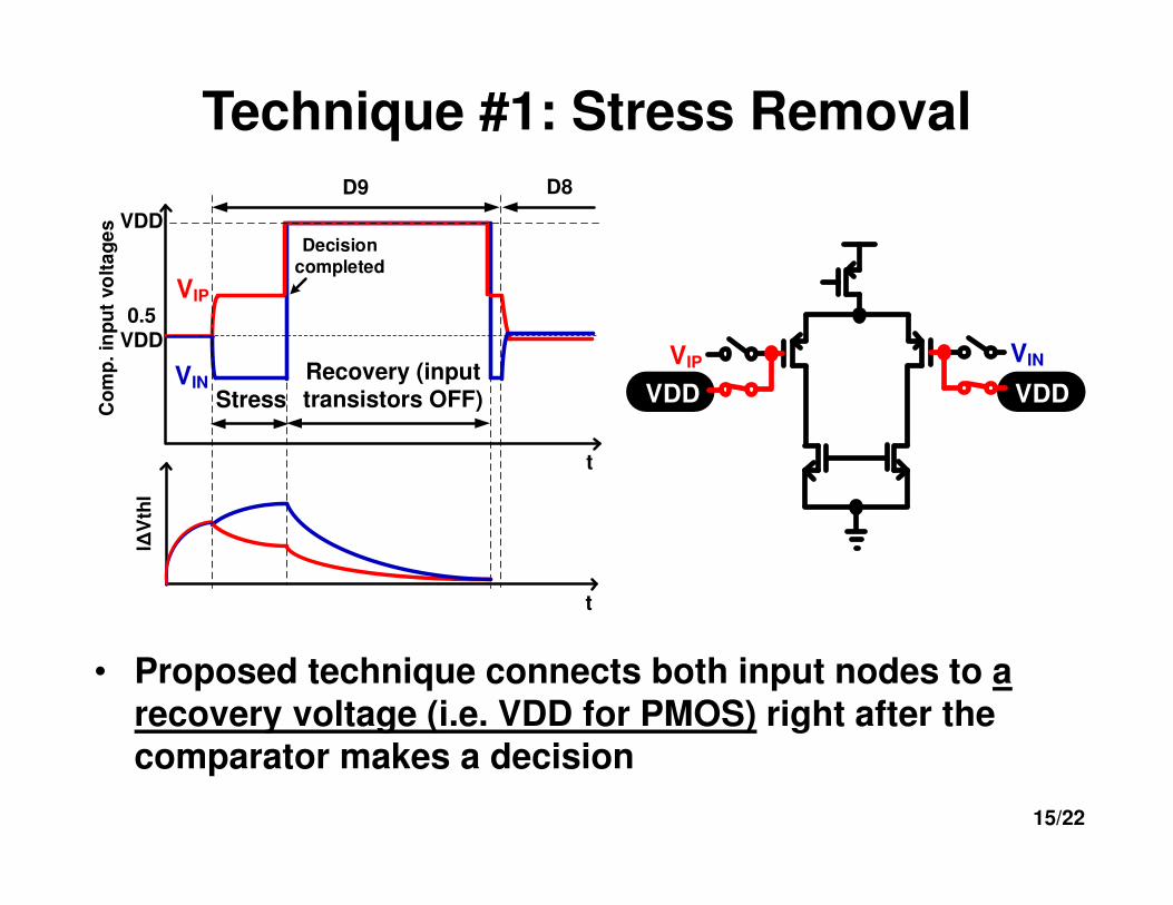
Proposed Dynamic Offset Cancellation Technique
• Temporarily connects both comparator input voltages to the same level ���� equalizes Vth shift
Comparator ref.: W. Liu, et al., ISSCC, 2010.
15/22
VDDRecovery (input transistors OFF)
lΔV
thl
VIP
D9
t
D8
Co
mp
. in
pu
t vo
lta
ge
s
t
VIN
VDD
0.5VDD
Stress
Decision completed
VIP VIN
VDD
Technique #1: Stress Removal
• Proposed technique connects both input nodes to a recovery voltage (i.e. VDD for PMOS) right after the comparator makes a decision

16/22
Technique #2: Stress Equalization
• Proposed technique connects both input nodes to the common mode voltage (i.e. VDD/2) right after the comparator makes a decision
Equalization
lΔV
thl
VIP
D9
t
D8
Co
mp
. in
pu
t vo
lta
ge
s
t
VIN
VDD
0.5VDD
Stress
Decision completed
ΔVth
ΔVth
VDD/2
VIP VIN
VDD/2
17/22
Agenda
• Impact of Short-term Vth Instability on SAR ADC operation
• Proposed Stress Mitigation Techniques
• SAR ADC Test-chip Measurement Results
• Conclusions

18/22
65nm SAR ADC Test Chip and Features

19/22
Measured DNL / INL
• 0.77 and 0.90 LSB improvement in DNL using stress removal and stress equalization, respectively
• Digital codes A~F show a large improvement in DNL
• INL remains relatively constant
20/22
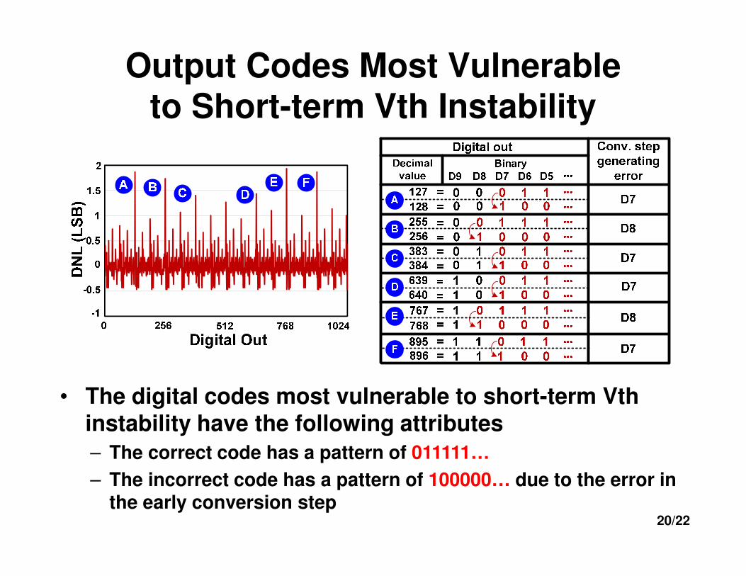
Output Codes Most Vulnerable to Short-term Vth Instability
• The digital codes most vulnerable to short-term Vth instability have the following attributes
– The correct code has a pattern of 011111…
– The incorrect code has a pattern of 100000… due to the error in the early conversion step

21/22
Measured FFT Results
• Subtle improvements in SNDR, ENOB, and SFDR observed after applying the proposed techniques
0
0 10
Po
wer
(dB
)
Frequency (kHz)20 30
-20
-40
-60
-80
-100
Typical SAR
w/ stress removal technique
w/ stress equalization technique
fIN: 2.205kHz, fSAMPLE: 80kS/s
-12040
Stress equalization
62.74
63.79
65.65
Typical SAR
Stress removal
SNDR(dB)
ENOB(bit)
SFDR(dB)
50.10
50.36
50.79
8.02
8.07
8.14
22/22
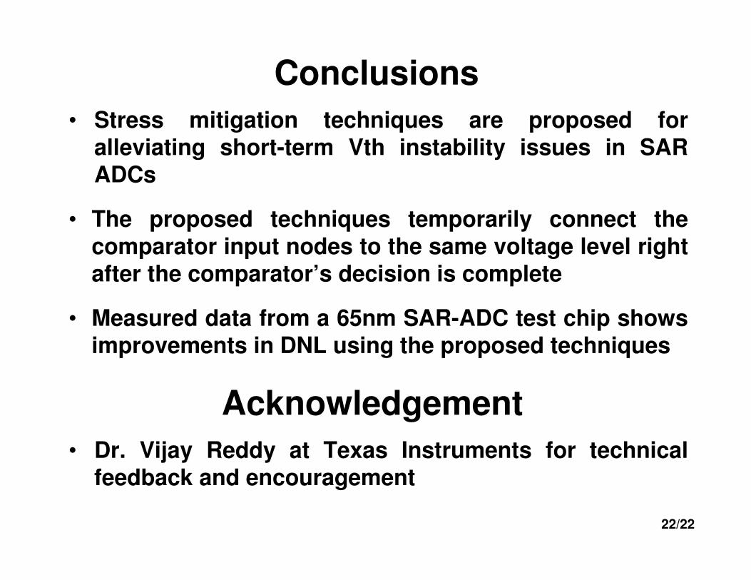
Conclusions
• Stress mitigation techniques are proposed foralleviating short-term Vth instability issues in SARADCs
• The proposed techniques temporarily connect thecomparator input nodes to the same voltage level rightafter the comparator’s decision is complete
• Measured data from a 65nm SAR-ADC test chip showsimprovements in DNL using the proposed techniques
Acknowledgement
• Dr. Vijay Reddy at Texas Instruments for technicalfeedback and encouragement


![PROCESS CHANGE NOTIFICATION - Mouser Electronics · Nch Vth[V] Nch Idr[μA/μm] Pch Vth[V] Pch Idr[μA/μm] Nch Tr. Vth-Idr Characteristic Pch Tr. Vth-Idr Characteristic Characteristic](https://static.fdocuments.us/doc/165x107/5ea9208bddcafa7fcd4fe0ba/process-change-notification-mouser-electronics-nch-vthv-nch-idram-pch.jpg)