
Chapter II Circuit Analysis...
53
ELEN-325. Introduction to Electronic Circuits: A Design-Oriented Approach Jose Silva-Martinez and Marvin Onabajo - - 1 Chapter II Circuit Analysis Fundamentals From a design engineer’s perspective, it is more relevant to understand a circuit’s operation and limitations than to find exact mathematical expressions or exact numerical solutions. Precise results can always be obtained through proper circuit simulations and through numerical analysis with software programs such as MATLAB or Maple. These tools cannot design the circuit for you, especially if you are dealing with analog circuits. Even though design automation programs can synthesize complete digital circuits, and progress is being made toward automating analog circuit design, engineers will still have to maintain knowledge about the functionality of circuits and systems. This chapter will review and introduce some basic circuit analysis methodologies that can be applied to gain insights into performance characteristics and design trade-offs. The approach will be to identify and utilize appropriate simplifications that enable approximate analysis, which is an essential skill when making initial component parameter selections for complex circuits and when performing optimizations.
Transcript of Chapter II Circuit Analysis...

ELEN-325. Introduction to Electronic Circuits: A Design-Oriented Approach Jose Silva-Martinez and Marvin Onabajo
- - 1
Chapter II
Circuit Analysis Fundamentals
From a design engineer’s perspective, it is more relevant to understand a circuit’s operation and limitations
than to find exact mathematical expressions or exact numerical solutions. Precise results can always be
obtained through proper circuit simulations and through numerical analysis with software programs such as
MATLAB or Maple.
These tools cannot design the circuit for you, especially if you are dealing with analog circuits. Even though
design automation programs can synthesize complete digital circuits, and progress is being made toward
automating analog circuit design, engineers will still have to maintain knowledge about the functionality of
circuits and systems.
This chapter will review and introduce some basic circuit analysis methodologies that can be applied to gain
insights into performance characteristics and design trade-offs.
The approach will be to identify and utilize appropriate simplifications that enable approximate analysis,
which is an essential skill when making initial component parameter selections for complex circuits and
when performing optimizations.

ELEN-325. Introduction to Electronic Circuits: A Design-Oriented Approach Jose Silva-Martinez and Marvin Onabajo
- - 2
II.i. DC and AC signals
A typical data acquisition system, such as the one shown in Figure 2.1, consists of a sensor (transducer), a
preamplifier, an analog filter, and the signal processor that typically includes an analog-to-digital converter.
The transducer detects the physical quantities to be measured and processed (temperature, pressure, glucose
level, frequency, wireless signal, etc.). Usually, the sensor’s output is a small signal (in the range of microvolts
to millivolts, i.e., in the range of 10-6 to 10-3 volts) and it must be amplified to fit within the linear input
amplitude range of the analog-to-digital converter.
The desired signal is typically accompanied by undesired information and random noise, the signal may be
“cleaned” through a frequency-selective filter that removes most of the undesired frequencies before the sensed
signal is converted into a digital format and further processed through dedicated software.
TransducerFilter (noise
removal)Preamp
Analog Processing Blocks
Electrical Signal
Digital
Signal
Processor
Digital Processing BlocksBiological
System
Analog-to-
Digital
Converter
Biological Signal
Fig. 2.1. Front-end of a typical bio-electronics system.
The electrical signals at the output of the transducer are normally composed of two components: the DC (direct
current) and AC (alternating current) signals.

ELEN-325. Introduction to Electronic Circuits: A Design-Oriented Approach Jose Silva-Martinez and Marvin Onabajo
- - 3
As shown in Figure 2.2, the DC component is a time-invariant quantity, while the AC component is a time-
variant quantity and usually this AC component contains the relevant information to be processed.
sAC(t) = SDD + sac(t) (2.0)
where SDD and sac denote the DC and AC signal components, respectively.
The following notations are used in this text to identify the nature of the signal components:
CAPITALCAPITAL labels represent only the DC component; e.g. SDD = 10V; IX = 2A.
lowercaselowercase stands for the AC component only; e.g. sac(t) = 2∙sin(t + ) V; isignal(t) = 2∙ej(t + ) A.
lowercaseCAPITAL stands for the combination of DC and AC components; e.g. sAC = SDD + sac(t); iSIGNAL = IX +
isignal .
Time
DC component
AC component
Amplitude
Time
AmplitudeDC + AC
SDD
sac(t)
sAC(t) = SDD+sac(t)
0 0
Fig. 2.2. Time domain signals: a) standalone DC and AC signals, b) combination of AC and DC signals.
ELEN-325. Introduction to Electronic Circuits: A Design-Oriented Approach Jose Silva-Martinez and Marvin Onabajo
- - 4
Although signals found in most real world scenarios are not periodic, the analysis and design of electronic
circuits is conducted based on periodic signals (sinusoidal waveforms, pulse train, triangular waveforms,
modulated waveforms, etc.) because many waveforms can be approximated with summations of periodic
signals.
The case of sinusoidal waveforms is especially interesting because periodic waveforms can be represented by a
Fourier series using sinusoids as a basis of functions. Many practical signals are continuous-time, periodic with
period T, and real functions f(t) are defined for all t; which allows representation with a simplified Fourier
series in the following form1:
T
tncosC)t(fn
n
200
, (2.1)
where 0 (2/T = 2f) is the fundamental frequency component in radians/sec used for series expansion.
f(t) has to be expressed as a linear combination of sine and cosine waveforms, but to simplify our discussion let
us ignore the sine functions. Cn is the nth Fourier coefficient, and it is computed as follows:
dtetfT
C
Tt
t
tjn
n
0
0
01
. (2.2)
The signal’s spectrum often has sinusoidal components at frequencies which are multiples of 0.
1 This is a simplified form of the Fourier series; the general form is
T;eC)t(f
n
tnj
n
2
00

ELEN-325. Introduction to Electronic Circuits: A Design-Oriented Approach Jose Silva-Martinez and Marvin Onabajo
- - 5
Eqs 2.1 and 2.2 are beneficial because they allow one to avoid analyzing circuits for all possible input signals.
Instead, it is preferred to analyze them for the case of sinusoidal inputs and, from those results, infer system
behavior for any other kind of input signal. This is the so-called frequency domain analysis.
In some areas such as power electronics, the time-domain analysis is more commonly used than the frequency
domain analysis. Pulse and impulse system responses are employed in those cases, and these topics will also be
partially covered in the following subsections.
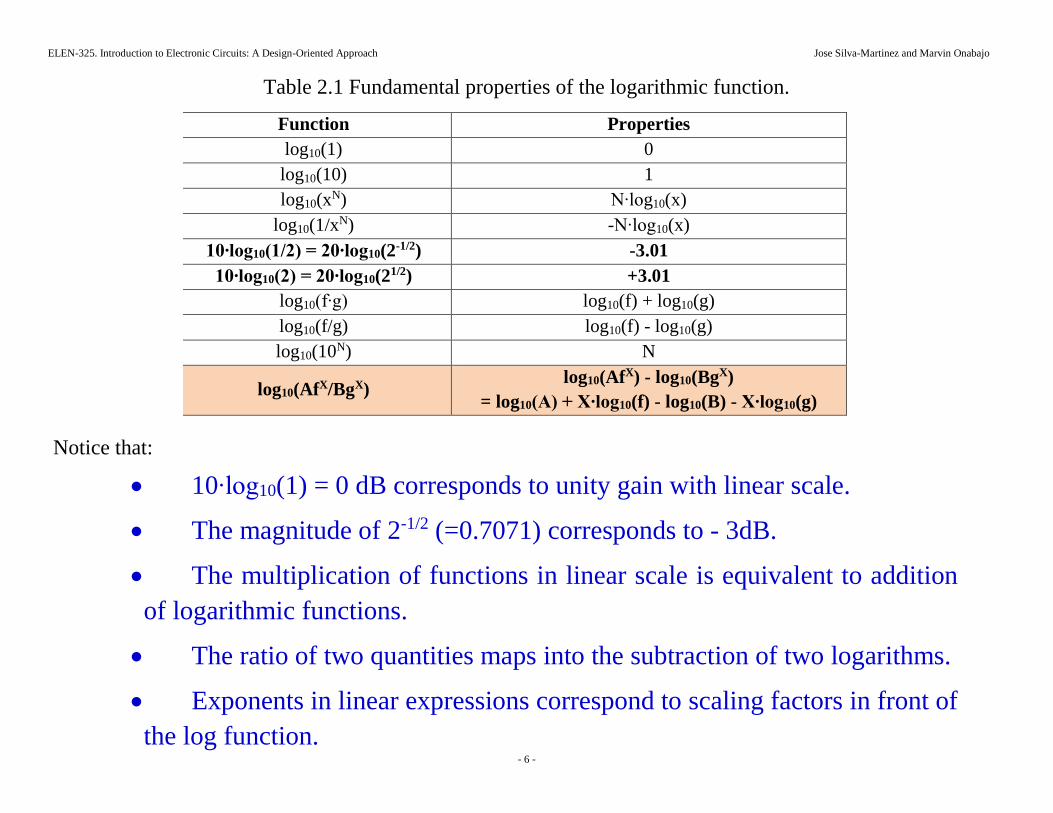
II.2. Decibels and Bode Plots
i) Magnitude response. The magnitude response is usually plotted in decibels (logarithmic scale), making it
easier to compare strong and weak signals. In general, it is often very convenient to use logarithmic scales in
cases where it is hard to visualize signal differences using linear scales. The magnitude in decibels (dB) of a
complex function f(x) is defined as:
)(log20)(log10 10
2
10 xfxfxfdB
, (2.3)
where |f(x)| stands for the magnitude of f(x).
The use of decibel notation (logarithmic scale) is very convenient when dealing with intricate transfer functions.
As an engineering student, you most likely already have a good background in logarithm operations, but
be sure to master these properties as they will be used extensively throughout your study of electronics.
ELEN-325. Introduction to Electronic Circuits: A Design-Oriented Approach Jose Silva-Martinez and Marvin Onabajo
- - 6
Table 2.1 Fundamental properties of the logarithmic function.
Notice that:
10∙log10(1) = 0 dB corresponds to unity gain with linear scale.
The magnitude of 2-1/2 (=0.7071) corresponds to - 3dB.
The multiplication of functions in linear scale is equivalent to addition
of logarithmic functions.
The ratio of two quantities maps into the subtraction of two logarithms.
Exponents in linear expressions correspond to scaling factors in front of
the log function.
Function Properties
log10(1) 0
log10(10) 1
log10(xN) N∙log10(x)
log10(1/xN) -N∙log10(x)
10∙log10(1/2) = 20∙log10(2-1/2) -3.01
10∙log10(2) = 20∙log10(21/2) +3.01
log10(f∙g) log10(f) + log10(g)
log10(f/g) log10(f) - log10(g)
log10(10N) N
log10(AfX/BgX) log10(AfX) - log10(BgX)
= log10(A) + X∙log10(f) - log10(B) - X∙log10(g)
ELEN-325. Introduction to Electronic Circuits: A Design-Oriented Approach Jose Silva-Martinez and Marvin Onabajo
- - 7
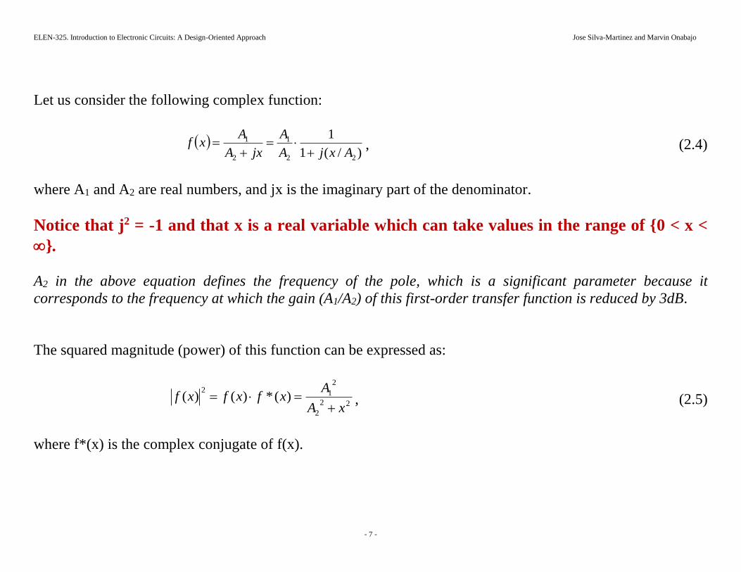
Let us consider the following complex function:
)/(1
1
22
1
2
1
AxjA
A
jxA
Axf
, (2.4)
where A1 and A2 are real numbers, and jx is the imaginary part of the denominator.
Notice that j2 = -1 and that x is a real variable which can take values in the range of {0 < x <
}.
A2 in the above equation defines the frequency of the pole, which is a significant parameter because it
corresponds to the frequency at which the gain (A1/A2) of this first-order transfer function is reduced by 3dB.
The squared magnitude (power) of this function can be expressed as:
22
2
2
12)(*)()(
xA
Axfxfxf
, (2.5)
where f*(x) is the complex conjugate of f(x).
ELEN-325. Introduction to Electronic Circuits: A Design-Oriented Approach Jose Silva-Martinez and Marvin Onabajo
- - 8
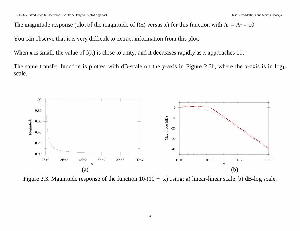
The magnitude response (plot of the magnitude of f(x) versus x) for this function with A1 = A2 = 10
You can observe that it is very difficult to extract information from this plot.
When x is small, the value of f(x) is close to unity, and it decreases rapidly as x approaches 10.
The same transfer function is plotted with dB-scale on the y-axis in Figure 2.3b, where the x-axis is in log10
scale.
0E+0 2E+2 4E+2 6E+2 8E+2 1E+3
x
0.00
0.20
0.40
0.60
0.80
1.00
Mag
nit
ude
1E+0 1E+1 1E+2 1E+3
x
-40
-30
-20
-10
0
Mag
nit
ud
e (d
B)
(a) (b)
Figure 2.3. Magnitude response of the function 10/(10 + jx) using: a) linear-linear scale, b) dB-log scale.

ELEN-325. Introduction to Electronic Circuits: A Design-Oriented Approach Jose Silva-Martinez and Marvin Onabajo
- - 9
To get more insight, let us more fully examine the previous transfer function.
22
2
2
12)(*)()(
xA
Axfxfxf
)(log*10)(log10 22
210
2
110 xAAxfdB
(2.6)
Notice that:
For x << A2 this equation can be approximated as 20∙log10(A1) - 20∙log10(A2) = 20∙log10(A1/A2), which is
equal to 0dB for the example case with A1 = A2 = 10.
For x = A2 = 10, the magnitude of f(x) becomes
|f(x)| = 10∙log10(A12) - 10∙log10(A2
2 ∙ 2)
= 20∙log10(10) - 10∙[log10(102) + log10(2)]
= 20∙log10(10) - 20∙log10(10) - 10∙log10(2)
= -10∙log10(2) = -3.01dB.
For x >> A2 equation 2.6 can be approximated as 10∙log10(A12) - 10∙log10(x2) = 20∙log10(10) - 20∙log10(x) dB.
Notice that the expression consists of a constant term and a negative term that decreases proportional to the -
20∙log10 function of x.
If we use a log10 scale on the x-axis, this corresponds to a straight line with a slope of -20, which agrees well
with the plot shown in Figure 2.3b for x >> A2 = 10. If x = 1000, then |f(1000)| ≈ 20 -20∙log10(103) = -40 dB,
which again fits well with the visual inspection that can be made in Figure 2.3b.
The transfer functions can be easily plotted in log10-dB scale after some additional observations.

ELEN-325. Introduction to Electronic Circuits: A Design-Oriented Approach Jose Silva-Martinez and Marvin Onabajo
- - 10
For frequencies beyond the pole frequency (A2 in the previous example) |f(x)| is approximately equal to
20∙log10(A1) - 20∙log10(x) dB; some values for the previous case are provided in Table 2.2.
Beyond the frequency of the pole, a one-decade increase on the x-axis corresponds to a gain change of -20 dB
(equivalently, this can be referred to as 20dB attenuation). Hence, the slope of the function with log10-scale on
the X-axis is -20dB/decade.
It can also be shown that an increase by a factor of 2 (1 octave) on the x-axis corresponds to an attenuation of
6dB for |f(x)| with x >> A2, leading to a slope of –6dB/octave.
Table 2.2 Example values for the magnitude of the 20∙log10(x) (x < 1) function in dB.
x
10-1 -20
10-2 -40
10-3 -60
10-4 -80
10-5 -100

ELEN-325. Introduction to Electronic Circuits: A Design-Oriented Approach Jose Silva-Martinez and Marvin Onabajo
- - 11
ii) The phase response of the first-order transfer function (solid line) displayed in Figure 2.4 requires a bit more
detailed analysis than for the magnitude response.
A complex expression can always be written in polar form: f(x) = |f(x)|ej,
is the phase of f(x) defined as = tan-1[Imaginary(f)/Real(f)].
Properties: (R and Im represent the real and imaginary parts, respectively).
Table 2.2 Relevant characteristics of complex numbers.
Function Evaluation
ImjRxf
RIm/tan
ImRxf
exfxf
f
j f
1
22
xgxf gfjexgxf
xg
xf
gfj
exg
xf
xgxgxg
xfxfxf
m
n
...
...
21
21
m
k
gk
n
i
fij
m
ne
xgxgxg
xfxfxf11
...
...
21
21

ELEN-325. Introduction to Electronic Circuits: A Design-Oriented Approach Jose Silva-Martinez and Marvin Onabajo
- - 12
To plot the phase of a transfer function by hand, you must first evaluate the phase of each individual term and
add the phases of the functions in the numerator while subtracting the phase of the functions in the denominator.
For instance, (A1 = A2 = 10):
)/(1
1
22
1
2
1
AxjA
A
jxA
Axf
;
)A/x(tan]jxA[Phase]A[Phase
]rDenominato[Phase]Numerator[Phase)]x(f[Phaseradians
2
1
21 0
. (2.7a)
This equation determines the phase in radians.
To convert the phase to degrees, you must multiply the value in radians by 360/2≈ 57.3, yielding
radiansdegrees
)]([3.57)]([ xfPhasexfPhase . (2.7b)
The phase plot shown in Figure 2.4 is a nonlinear function. Some observations will allow us to approximate this
function with simpler but quite useful piecewise linear functions:
The phase at x = 0 is 0 degrees because the function is real and positive for this value of x. Negative real
functions have an initial phase of radians (or 180 degrees) at x = 0.
The phase shift of f(x) at the location of the pole x = A2 is -45 degrees.
The phase at x = is - radians (or -90 degrees).
If we evaluate the derivative of the phase response at the pole’s location (x = A2), it takes on the larger value
of more than -45 degrees/decade.

ELEN-325. Introduction to Electronic Circuits: A Design-Oriented Approach Jose Silva-Martinez and Marvin Onabajo
- - 13
Figure 2.4. Phase response for the transfer function in Eq. 2.4 with A1 = A2 = 10.
Let us approximate the phase response (Eq. 2.7a) of the transfer function by a piecewise linear function such
that below x = 0.1∙A2 = 1 where the phase is approximated as 0 degrees,
Above x = 10∙A2 = 100, it is approximated by -90 degrees.
The phase around x = A2 = 10 (the frequency of the pole) is approximated to have a slope of -45 degrees per
decade. Both the exact phase response (solid trace) and the piecewise linear approximation (dashed trace) are
shown in Figure 2.4. The largest error introduced by the approximation is +/-5.7 degrees, which is acceptable
for most hand calculations.
The previously discussed properties are also valid for the general case.

ELEN-325. Introduction to Electronic Circuits: A Design-Oriented Approach Jose Silva-Martinez and Marvin Onabajo
- - 14
For instance, consider the following complex function:
xjAA
Axf
32
1)(
. (2.8)
This equation can be rearranged to:
jx
A
A
A
A
xf
3
2
3
1
)( . (2.8b)
Therefore, this equation becomes similar to Eq. 2.5., and can be expressed in dB as:
2
2
3
2
2102
3
2
110 log10log10)( x
A
A
A
Axf
dB . (2.9)
Now, the transfer function can be easily sketched by examining each part separately for the different ranges that
variable x can be in while noting that:

ELEN-325. Introduction to Electronic Circuits: A Design-Oriented Approach Jose Silva-Martinez and Marvin Onabajo
- - 15
3
210
3
110
2
102
3
2
110
3
22
210
2
110
3
22
210
2
1102
3
2
2102
3
2
110
202010
310
10101010
A
Axifxlog
A
Alogxlog
A
Alog
A
AxifAlogAlog
A
AxifAlogAlog
A
Alog
A
Alog
)x(fdB (2.10)
It should be evident that the parameter A2/A3 plays an important role in shaping the transfer function, since this
parameter is in fact the location of the pole.
3 dB
exact
Appoximation
A2/A3
x(log)
20·log10(A1/A2)
-20 dB/decade
Fig. 2.5. Plot of the transfer function described by Eq. 2.9 with its piecewise linear approximation.
The maximum error of -3 dB occurs at the frequency (A2/A3) of the pole.
Since f(x) is complex, we have to consider its phase response as well. Considering f(x) given by Eq. 2.8, the
phase response is

ELEN-325. Introduction to Electronic Circuits: A Design-Oriented Approach Jose Silva-Martinez and Marvin Onabajo
- - 16
x
A
A
AA
xAPhasexfPhase
2
31
32
1
1 tantan][)]([. (2.11)
For x = 0, the phase shift presented by the circuit is 0 degrees.
A2/A3=10
The phase shift is -0.785 radians (= -45 degrees) for x = A2/A3; the phase shift when x approaches infinity is -
1.57 radians (-90 degrees).
Notice that the phase shift is close to the limits of the piecewise linear approximation (around 0º when x ≈
0.1∙A2/A3, and around -90º when x ≈ 10∙A2/A3).
The transition from 0 to -90 degrees takes place within approximately two decades around the system’s pole x =
A2/A3. The slope of the phase around a pole is approximately –45 degrees/decade, and the maximum error
is +/-5.7 degrees. Additionally, the phase shift is -45 degrees at the pole (x = A2/A3).

ELEN-325. Introduction to Electronic Circuits: A Design-Oriented Approach Jose Silva-Martinez and Marvin Onabajo
- - 17
iii) Magnitude and phase of a general function.
jxA
A
jxA
A
A
A
xjAA
xjAAxf
4
3
2
1
4
2
43
21)(. (2.12)
A1/A2 and A3/A4 are termed the zero and pole of the complex function, respectively.
2
2
4
310
2
2
2
110
2
4
210 log10log10log10)( x
A
Ax
A
A
A
Axf
(dB) . (2.13)
Similar to the case of a single pole function, the three terms of this expression can be approximated for different
ranges of x.

ELEN-325. Introduction to Electronic Circuits: A Design-Oriented Approach Jose Silva-Martinez and Marvin Onabajo
- - 18
As an example, let us consider A1/A2 < A3/A4
These results can be plotted by using the piecewise linear approximation shown in Figure 2.6.
3 dB
A2/A1
x(log)20·log10(A1/A3)
20 dB/decade
A3/A4
3 dB
20·log10(A2/A4)
Fig. 2.6. Magnitude response of a function with a pole-zero pair where zero location < pole location.

ELEN-325. Introduction to Electronic Circuits: A Design-Oriented Approach Jose Silva-Martinez and Marvin Onabajo
- - 19
The phase in radians can be obtained through the following rearrangements:
.tantan
)(
3
41
1
21
4
3
2
1
4
3
2
1
A
xA
A
xA
jxA
APhasejx
A
APhase
jxA
A
jxA
A
PhasexfPhase
(2.15)
A2/A
1
x(log)0 degrees
A3/A
4
90 degrees
45 degrees
Fig. 2.7. Phase response of the first-order transfer function under examination.
ELEN-325. Introduction to Electronic Circuits: A Design-Oriented Approach Jose Silva-Martinez and Marvin Onabajo
- - 20
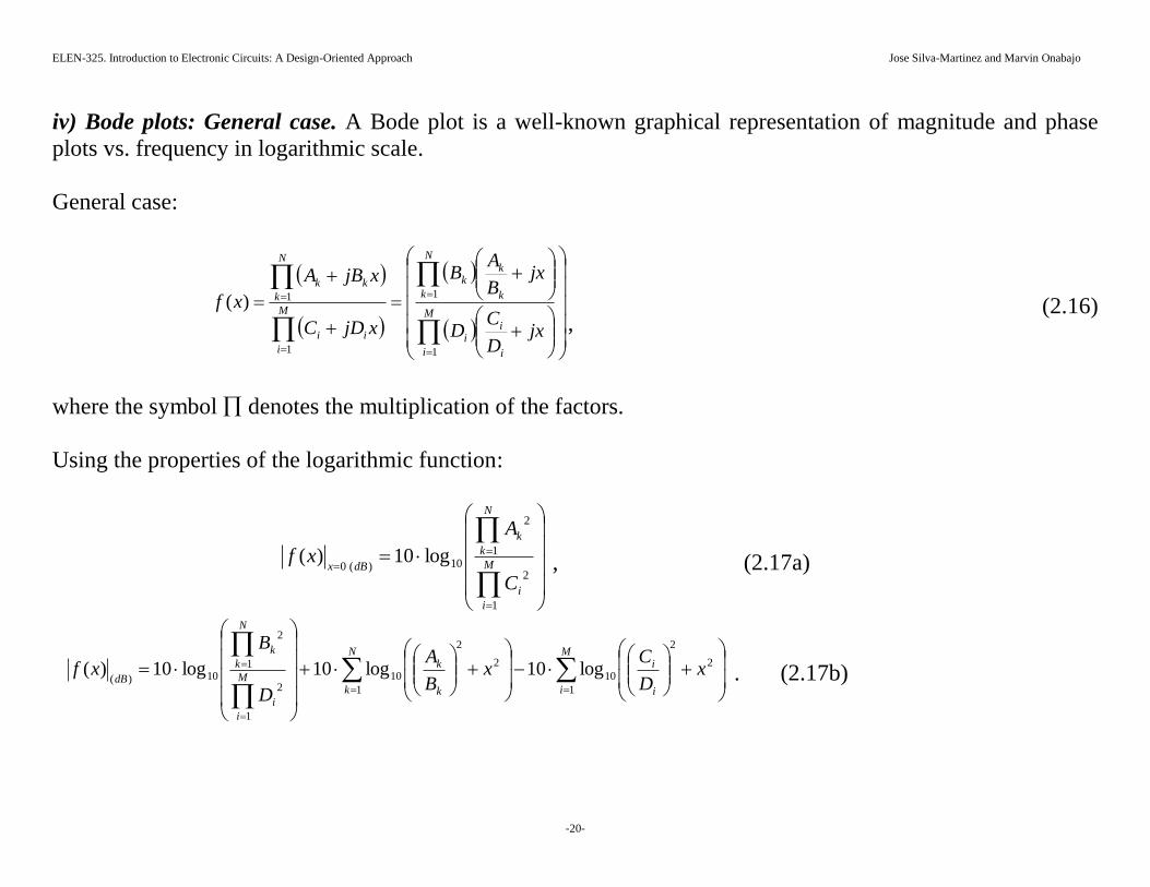
iv) Bode plots: General case. A Bode plot is a well-known graphical representation of magnitude and phase
plots vs. frequency in logarithmic scale.
General case:
M
i i
ii
N
k k
kk
M
i
ii
N
k
kk
jxD
CD
jxB
AB
xjDC
xjBA
xf
1
1
1
1)(
, (2.16)
where the symbol denotes the multiplication of the factors.
Using the properties of the logarithmic function:
M
i
i
N
k
k
dBx
C
A
xf
1
2
1
2
10)(0log10)( , (2.17a)
M
i i
iN
k k
k
M
i
i
N
k
k
dBx
D
Cx
B
A
D
B
xf1
2
2
10
1
2
2
10
1
2
1
2
10)(log10log10log10)( . (2.17b)

ELEN-325. Introduction to Electronic Circuits: A Design-Oriented Approach Jose Silva-Martinez and Marvin Onabajo
- - 21
Note that 2.17a is only valid at DC (x = 0), while 2.17b holds at any frequency. Generally, the complete
expression must be considered because we do not have information about the location of the poles and/or zeros.
However, simplifications can be made when relative pole/zero locations are known.
Also notice that we normalized the functions with respect to the zeros and poles to make an analysis by
inspection easier. Some insightful characteristics involving the above equations follow:
1. By setting x = 0 in Eq. 2.17b, the DC gain of the function (magnitude of the transfer function at x = 0) can
be obtained. This is the starting point of the overall magnitude response on the y-axis, and it depends on
the coefficients Ak and Ci since other terms will cancel each other.
2. The zeros and poles must be identified. After frequency x = 0, each zero of the transfer function will
increase the magnitude at a rate of 20 dB/decade. Similarly, each pole will decrease the magnitude of the
function by -20dB/decade after the pole’s location on the x-axis. Since a dB-scale is used on the y-axis
together with logarithmic scale on the x-axis, the aforementioned effects of poles and zeros on the
magnitude can be added algebraically.
3. At a given x-value, the roll-off (slope) of the magnitude can be easily obtained by the following equation:
dB20xbelowpoles of #xbelowzeros of #xx f of slope 000 (2.18)
4. Finally, you can evaluate the function for x → to see that the final value depends on several factors:
a. If the number of zeros is greater than the number of poles, the transfer function goes to infinity
(positive infinite in dB) as x → .
b. If the number of poles is greater than the zeros, which is the typical case in electronics, the final
value is zero (negative infinite in dB) when x → .
c. In case the number of poles and zeros are equal, then the magnitude’s final value is a function of the
coefficients Bk and Di.
ELEN-325. Introduction to Electronic Circuits: A Design-Oriented Approach Jose Silva-Martinez and Marvin Onabajo
- - 22
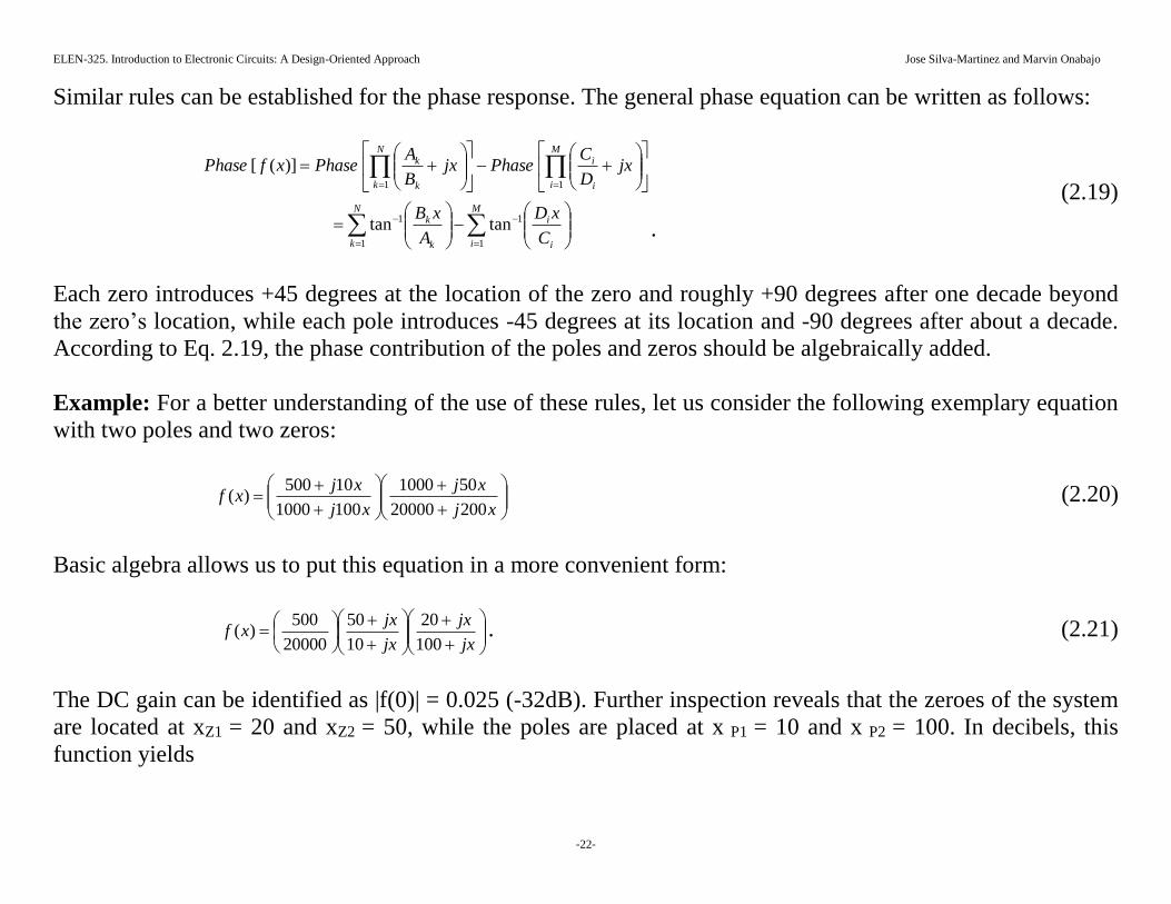
Similar rules can be established for the phase response. The general phase equation can be written as follows:
M
i i
iN
k k
k
M
i i
iN
k k
k
C
xD
A
xB
jxD
CPhasejx
B
APhasexfPhase
1
1
1
1
11
tantan
)]([
.
(2.19)
Each zero introduces +45 degrees at the location of the zero and roughly +90 degrees after one decade beyond
the zero’s location, while each pole introduces -45 degrees at its location and -90 degrees after about a decade.
According to Eq. 2.19, the phase contribution of the poles and zeros should be algebraically added.
Example: For a better understanding of the use of these rules, let us consider the following exemplary equation
with two poles and two zeros:
xj
xj
xj
xjxf
20020000
501000
1001000
10500)( (2.20)
Basic algebra allows us to put this equation in a more convenient form:
jx
jx
jx
jxxf
100
20
10
50
20000
500)( . (2.21)
The DC gain can be identified as |f(0)| = 0.025 (-32dB). Further inspection reveals that the zeroes of the system
are located at xZ1 = 20 and xZ2 = 50, while the poles are placed at x P1 = 10 and x P2 = 100. In decibels, this
function yields

ELEN-325. Introduction to Electronic Circuits: A Design-Oriented Approach Jose Silva-Martinez and Marvin Onabajo
- - 23
22
10
22
10
22
10
22
10)(100log1010log1050log1020log1032)( xxxxdBxf
dB . (2.22)
x(log)-10
|f(x)| (dB)
10 102
-20
-40
-32
Magnitude
(dB)
Fig. 2.8. Magnitude response of the complex transfer function given by Eq. 2.21.
ELEN-325. Introduction to Electronic Circuits: A Design-Oriented Approach Jose Silva-Martinez and Marvin Onabajo
- - 24
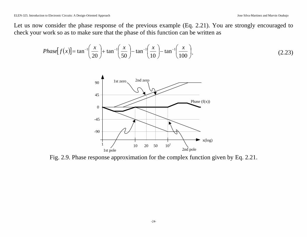
Let us now consider the phase response of the previous example (Eq. 2.21). You are strongly encouraged to
check your work so as to make sure that the phase of this function can be written as
100tan
10tan
50tan
20tan 1111 xxxx
xfPhase . (2.23)
1x(log)
0
10 10220 50
-45
-90
45
90
Phase (f(x))
1st pole 2nd pole
1st zero 2nd zero
Fig. 2.9. Phase response approximation for the complex function given by Eq. 2.21.
ELEN-325. Introduction to Electronic Circuits: A Design-Oriented Approach Jose Silva-Martinez and Marvin Onabajo
- - 25
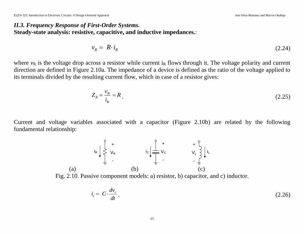
II.3. Frequency Response of First-Order Systems.
Steady-state analysis: resistive, capacitive, and inductive impedances.:
RR iRv (2.24)
where vR is the voltage drop across a resistor while current iR flows through it. The voltage polarity and current
direction are defined in Figure 2.10a. The impedance of a device is defined as the ratio of the voltage applied to
its terminals divided by the resulting current flow, which in case of a resistor gives:
Ri
vZ
R
RR . (2.25)
Current and voltage variables associated with a capacitor (Figure 2.10b) are related by the following
fundamental relationship:
+
VR
-
iR
+
VC
-
iC
+
VL
-
iL
(a) (b) (c)
Fig. 2.10. Passive component models: a) resistor, b) capacitor, and c) inductor.
dt
dvCi c
c . (2.26)
ELEN-325. Introduction to Electronic Circuits: A Design-Oriented Approach Jose Silva-Martinez and Marvin Onabajo
- - 26
When expressing the AC voltage applied at the capacitor terminals in the general complex form vc = VC∙ejt, the
expression for the current flowing through it can be derived from Eq. 2.26 as
cc vCji . (2.27)
sCCji
vZ
c
cc
11
(2.28)
where (=2f) is the signal frequency in radians/sec.
To simplify the algebra, usually the frequency variable is defined as s = j. Notice that s is an imaginary
variable.
At = 0, the magnitude of the capacitive impedance is infinite (open circuit).
Impedance approaches zero at very high frequency
ELEN-325. Introduction to Electronic Circuits: A Design-Oriented Approach Jose Silva-Martinez and Marvin Onabajo
- - 27
Following a similar procedure as for the capacitor, the impedance of the inductor under steady state conditions
can also be found easily.
dt
diLv L
L (2.29)
where L is the inductance in henry (H). If the inductor’s current has the general complex form iL = IL∙ejt, then
LL iLjv . (2.30)
This voltage generated across the inductor and the current flowing through it are +90 degrees out of phase. The
impedance of the inductor can be derived from Eq. 2.30 as
sLLji
vZ
L
LL . (2.31)
Contrary to the case of the capacitor, the inductor presents very small impedance across its terminals at low
frequency (ZL = 0 at DC) and very high impedance (open circuit) at very high frequencies.

ELEN-325. Introduction to Electronic Circuits: A Design-Oriented Approach Jose Silva-Martinez and Marvin Onabajo
- - 28
Voltage Divider. By using basic circuit theory (KVL) it can be easily shown that the voltage across the
grounded impedance Z2 is given by the following expression:
21
20
ZZ
Z
v
v
i . (2.32)
If the nonzero impedances Z1 and Z2 are of the same type (either real or imaginary), the amplitude of the output
voltage v0 is smaller than the amplitude of the applied signal vi.
The frequency response of some of these functions is analyzed next.
Z1
Z2
vi v0
vi v0
R2
R1
(a) (b)
Fig. 2.11. Voltage divider: a) general scheme and b) resistive voltage divider.
Let us first consider the case of a simple resistive divider shown in Figure 2.11b. The voltage gain in this case is
21
20
RR
R
v
v
i . (2.33)
Since the resistors are ideally voltage and frequency independent elements, the voltage gain of the resistive
voltage divider is a real number with a magnitude less than unity and a phase shift of zero degrees for all
frequencies. Thus, the output signal is an attenuated replica of the incoming signal.

ELEN-325. Introduction to Electronic Circuits: A Design-Oriented Approach Jose Silva-Martinez and Marvin Onabajo
- - 29
For these shown simulation results, R1 = 1k and R2 = {100, 1.1 k, and 2.1k}. The voltage attenuation
factors are 100/1100 (-20.8 dB), 1100/2100 (-5.6 dB), and 2100/3100 (-3.4 dB) for the respective values of R2.
1E+1 1E+2 1E+3 1E+4 1E+5
Frequency (Hz)
-25
-20
-15
-10
-5
0
Volt
age
Gai
n (
dB
)
Fig. 2.12. Magnitude response of the resistive voltage divider.
The output voltage (across Z2) is the difference between the input voltage and the voltage drop across the series
impedance Z1. Hence, the larger the series resistance Z2 is, the larger the voltage drop across it, and the
smaller the output voltage will be. Notice that if a voltage divider is formed by resistors, then
2
10
1R
R
vv i
. (2.33b)
R1 = 1k, R2 = 2.1k
R1 = 1k, R2 = 1.1k
R1 = 1k, R2 = 100

ELEN-325. Introduction to Electronic Circuits: A Design-Oriented Approach Jose Silva-Martinez and Marvin Onabajo
- - 30
First-order low-pass transfer function. If Z2 is replaced by a capacitor (C2) in the voltage divider of Figure 2.11 while keeping Z2 = R2, then the circuit
becomes a low-pass filter.
Low-pass filters are frequently used to suppress undesired high-frequency signal components and noise.
In audio applications, for example, the signal bandwidth approximately is 20kHz, and received signals above
that frequency should be suppressed before the information is converted into digital format for further
processing and recording.
vi v0
R1+
vC2
-
+ vR1 -
C2
Fig. 2.13. First-order low-pass filter.
The voltage gain of the resulting first-order system becomes
21
21
21
21
2
1
2
21
20
1
1
1
1
1
1
CRs
CR
CRj
CR
CjR
Cj
ZZ
Z
v
v
i
. (2.34)
It should be evident that the voltage gain has become a complex function of the frequency variable due to the
combination of the resistor (real impedance) and the capacitor (imaginary impedance). For very low frequencies
(≈ 0), the transfer function is positive and real (unity in this case). At the frequency of the pole (= p =
ELEN-325. Introduction to Electronic Circuits: A Design-Oriented Approach Jose Silva-Martinez and Marvin Onabajo
- - 31
1/[R1C2]), the transfer function becomes equal to p/(p + jp) =1/(1 + j), and the magnitude of the transfer
function is equal to 0.7071 (-3 dB). On the other hand, the phase shift between output and input is close to zero
at very low frequencies and -45 degrees at = p. For frequencies beyond p = 1/(R1C2), the transfer function is
dominated by the factor 1/jR1C2), causing the magnitude of the transfer function to decrease as the signal
frequency increases. The magnitude of the transfer function reduces at high frequencies because the capacitive
impedance is lower at high frequency. This is explained by the fact that the value of the resistive impedance is
greater than that of the capacitive impedance beyond p. Consequently, most of the input signal appears across
the larger impedance, which is the resistor when >> p. The regions of operation for this example filter can
be summarized as follows:
.1
log201
log20
,1
3
,1
0
log10
21
10
21
10
21
212
010
CRif
CR
CRifdB
CRifdB
v
v
i
(2.35)
The two regions of operation (pass-band with flat response and stop-band with roll-off response) can be
identified by observing the log-log plot depicted in Figure 2.14a for two example cases: p = 1/(R1C2) = 2∙300
rad/sec (fp = 300Hz) and p = 1/(R1C2) = 2∙10000 rad/sec (fp = 10kHz). Recall that the pole’s frequency p is
determined by the R1C2 product.
It is interesting to revisit the physical explanation for the behavior of this first-order low-pass circuit. For low
frequencies (<< 1/[R1C2]), the series resistance R1 is much smaller than the magnitude of the grounded
capacitor impedance given by 1/C2). Since the input voltage is split between the two elements (vin = vR1 + vC2)
and one of the impedances is much greater than the other one, most of the voltage will appear across the higher
impedance. Most of the input voltage is absorbed by the capacitor at low frequencies, leading to vC2 = vin at DC
(unity gain and zero phase shift). At = 1/(R1C2), the magnitudes of both impedances are equal, and the input

ELEN-325. Introduction to Electronic Circuits: A Design-Oriented Approach Jose Silva-Martinez and Marvin Onabajo
- - 32
voltage is equally split between the two elements, resulting in |vR1| = |vC2| = 0.7vin since the current flowing
through both elements is the same. But, the resistance is real and the capacitive impedance is imaginary. At
high frequencies, the impedance of the capacitor reduces further, and most of the input signal is then absorbed
by the series resistor. The higher the frequency is, the smaller the capacitive impedance and the larger the
attenuation factor will be. At very high frequencies, the capacitor’s impedance becomes extremely small
(practically zero) and effectively shortens the output node to ground (i.e. the capacitor forms a short circuit at
= ).
1E+1 1E+2 1E+3 1E+4 1E+5
Frequency (Hz)
-50
-40
-30
-20
-10
0
Volt
age
Gai
n (
dB
)
Fig. 2.14a. Magnitude response of the first-order low-pass filter for two cases:
1/(R1C2) = 2∙300 and 1/(R1C2) = 2∙10000.

ELEN-325. Introduction to Electronic Circuits: A Design-Oriented Approach Jose Silva-Martinez and Marvin Onabajo
- - 33
1E+1 1E+2 1E+3 1E+4 1E+5
Frequency (Hz)
-90.0
-67.5
-45.0
-22.5
0.0
Phas
e (D
egre
es)
Fig. 2.14b. Phase response of the first-order low-pass filter for the two example cases.
The phase response (in radians) of the low-pass filter circuit’s transfer function is obtained from 2.34 as
21
1
21
211 tan01
1
tan CR
CRj
CR
v
vPhase
i
o
. (2.35)
The corresponding phase plot is depicted in Figure 2.14b. As discussed in the previous subsection, the phase
variation is mainly allocated within two decades around the pole’s frequency (0.1P < <P). For the case
P = 1/(R1C2) = 2∙10000 rad/sec (fP = 10kHz), the phase shift transitions from 0 to -90 degrees within the
frequency range of 1kHz - 100kHz, being exactly -45 degrees at fP = 10kHz.
Of course, the magnitude and phase plots are correlated with the time response of the circuit. If a sinusoidal
signal is applied at the input of the low-pass filter, which is a linear system, then the output will also be a
sinusoidal function but with a different amplitude and different phase. In case the frequency of the input signal
is below the frequency of the pole, the amplitude of the output signal is very close to the amplitude of the input
ELEN-325. Introduction to Electronic Circuits: A Design-Oriented Approach Jose Silva-Martinez and Marvin Onabajo
- - 34
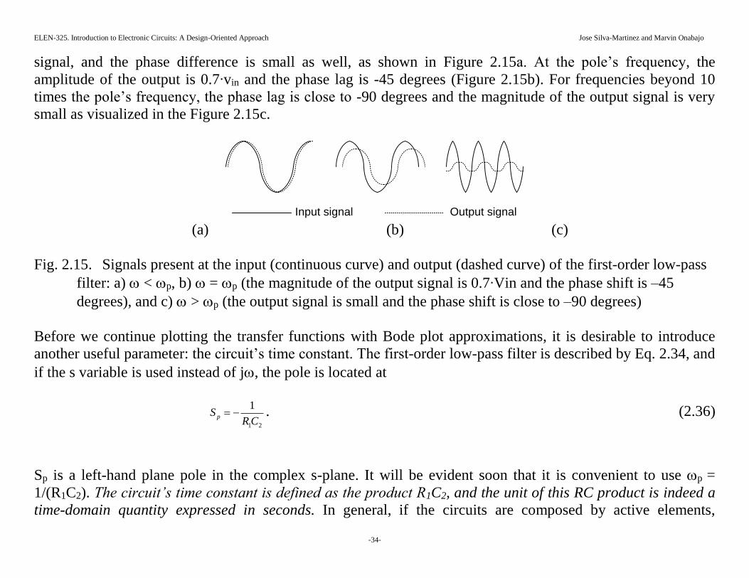
signal, and the phase difference is small as well, as shown in Figure 2.15a. At the pole’s frequency, the
amplitude of the output is 0.7∙vin and the phase lag is -45 degrees (Figure 2.15b). For frequencies beyond 10
times the pole’s frequency, the phase lag is close to -90 degrees and the magnitude of the output signal is very
small as visualized in the Figure 2.15c.
Input signal Output signal (a) (b) (c)
Fig. 2.15. Signals present at the input (continuous curve) and output (dashed curve) of the first-order low-pass
filter: a) < p, b) = p (the magnitude of the output signal is 0.7∙Vin and the phase shift is –45
degrees), and c) > p (the output signal is small and the phase shift is close to –90 degrees)
Before we continue plotting the transfer functions with Bode plot approximations, it is desirable to introduce
another useful parameter: the circuit’s time constant. The first-order low-pass filter is described by Eq. 2.34, and
if the s variable is used instead of j, the pole is located at
21
1
CRS p . (2.36)
Sp is a left-hand plane pole in the complex s-plane. It will be evident soon that it is convenient to use p =
1/(R1C2). The circuit’s time constant is defined as the product R1C2, and the unit of this RC product is indeed a
time-domain quantity expressed in seconds. In general, if the circuits are composed by active elements,
ELEN-325. Introduction to Electronic Circuits: A Design-Oriented Approach Jose Silva-Martinez and Marvin Onabajo
- - 35
capacitors, and resistors, then the frequency of both poles and zeros can be determined by corresponding RC
products (time constants).
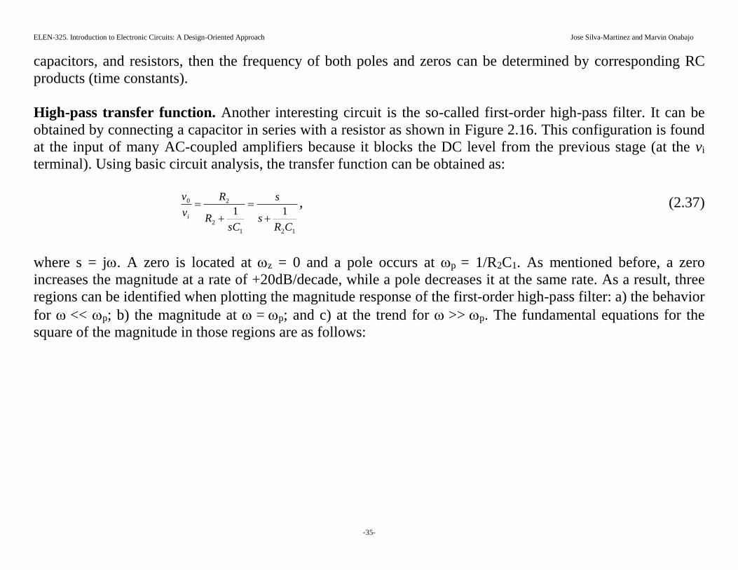
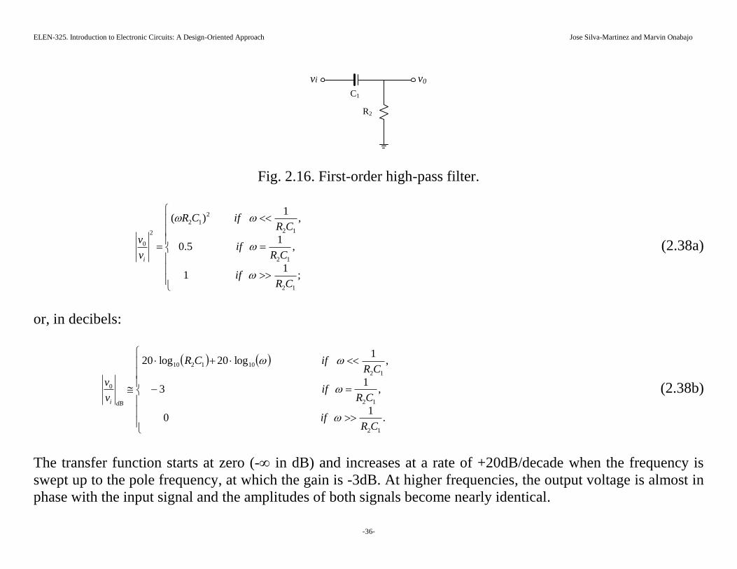
High-pass transfer function. Another interesting circuit is the so-called first-order high-pass filter. It can be
obtained by connecting a capacitor in series with a resistor as shown in Figure 2.16. This configuration is found
at the input of many AC-coupled amplifiers because it blocks the DC level from the previous stage (at the vi
terminal). Using basic circuit analysis, the transfer function can be obtained as:
121
2
20
11
CRs
s
sCR
R
v
v
i
, (2.37)
where s = j. A zero is located at z = 0 and a pole occurs at p = 1/R2C1. As mentioned before, a zero
increases the magnitude at a rate of +20dB/decade, while a pole decreases it at the same rate. As a result, three
regions can be identified when plotting the magnitude response of the first-order high-pass filter: a) the behavior
for << p; b) the magnitude at =p; and c) at the trend for >> p. The fundamental equations for the
square of the magnitude in those regions are as follows:
ELEN-325. Introduction to Electronic Circuits: A Design-Oriented Approach Jose Silva-Martinez and Marvin Onabajo
- - 36
vi v0
C1
R2
Fig. 2.16. First-order high-pass filter.
;1
1
,1
5.0
,1
)(
12
12
12
2
12
2
0
CRif
CRif
CRifCR
v
v
i
(2.38a)
or, in decibels:
.1
0
,1
3
,1
log20log20
12
12
12
101210
0
CRif
CRif
CRifCR
v
v
dBi
(2.38b)
The transfer function starts at zero (- in dB) and increases at a rate of +20dB/decade when the frequency is
swept up to the pole frequency, at which the gain is -3dB. At higher frequencies, the output voltage is almost in
phase with the input signal and the amplitudes of both signals become nearly identical.

ELEN-325. Introduction to Electronic Circuits: A Design-Oriented Approach Jose Silva-Martinez and Marvin Onabajo
- - 37
It is important to notice that the capacitive impedance is extremely large at DC and low frequencies, hence most
of the input signal is absorbed by this element when it is in the direct signal path from the input to the output.
Therefore, the voltage drop across the resistor is very small at low frequencies. At very high frequencies, the
capacitive impedance decreases and can even be considered as zero for quick estimates at frequencies much
larger than the pole frequency. In this case, the input signal is mostly absorbed by the resistor, which leads to a
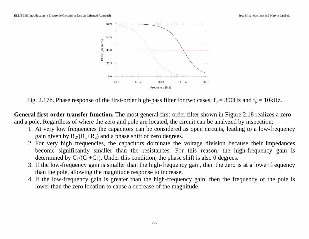
voltage gain that is close to unity (0dB). The magnitude and phase responses of the filter depicted in Figure 2.17
are for two cases: p = 1/R1C2 = 2∙300 rad/sec and p = 1/R1C2 = 2∙10000 rad/sec, where the -3dB
frequencies occur when the plots cross the horizontal dashed lines.
1E+1 1E+2 1E+3 1E+4 1E+5
Frequency (Hz)
-60
-50
-40
-30
-20
-10
0
Volt
age
Gai
n (
dB
)
Fig. 2.17a. Magnitude response of the first-order high-pass filter for two cases: fp = 300Hz and fp = 10kHz.
ELEN-325. Introduction to Electronic Circuits: A Design-Oriented Approach Jose Silva-Martinez and Marvin Onabajo
- - 38
1E+1 1E+2 1E+3 1E+4 1E+5
Frequency (Hz)
0.0
22.5
45.0
67.5
90.0
Phas
e (D
egre
es)
Fig. 2.17b. Phase response of the first-order high-pass filter for two cases: fp = 300Hz and fp = 10kHz.
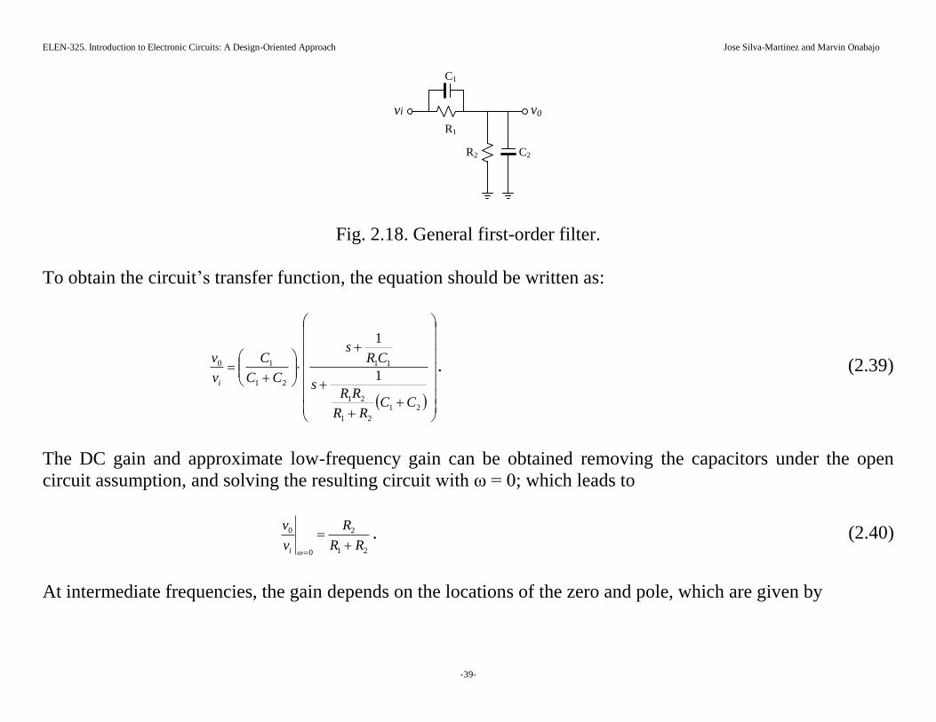
General first-order transfer function. The most general first-order filter shown in Figure 2.18 realizes a zero
and a pole. Regardless of where the zero and pole are located, the circuit can be analyzed by inspection:
1. At very low frequencies the capacitors can be considered as open circuits, leading to a low-frequency
gain given by R2/(R1+R2) and a phase shift of zero degrees.
2. For very high frequencies, the capacitors dominate the voltage division because their impedances
become significantly smaller than the resistances. For this reason, the high-frequency gain is
determined by C1/(C1+C2). Under this condition, the phase shift is also 0 degrees.
3. If the low-frequency gain is smaller than the high-frequency gain, then the zero is at a lower frequency
than the pole, allowing the magnitude response to increase.
4. If the low-frequency gain is greater than the high-frequency gain, then the frequency of the pole is
lower than the zero location to cause a decrease of the magnitude.
ELEN-325. Introduction to Electronic Circuits: A Design-Oriented Approach Jose Silva-Martinez and Marvin Onabajo
- - 39
vi v0
C1
R2 C2
R1
Fig. 2.18. General first-order filter.
To obtain the circuit’s transfer function, the equation should be written as:
21
21
21
11
21
10
1
1
CCRR
RRs
CRs
CC
C
v
v
i
. (2.39)
The DC gain and approximate low-frequency gain can be obtained removing the capacitors under the open
circuit assumption, and solving the resulting circuit with ω = 0; which leads to
21
2
0
0
RR
R
v
v
i
. (2.40)
At intermediate frequencies, the gain depends on the locations of the zero and pole, which are given by

ELEN-325. Introduction to Electronic Circuits: A Design-Oriented Approach Jose Silva-Martinez and Marvin Onabajo
- - 40
.
1
,1
21
21
21
11
CCRR
RR
CR
p
z
(2.41)
Finally, the magnitude of the transfer function at high frequencies can be obtained by evaluating the transfer
function for = , which results in
21
10
CC
C
v
v
i
. (2.42)
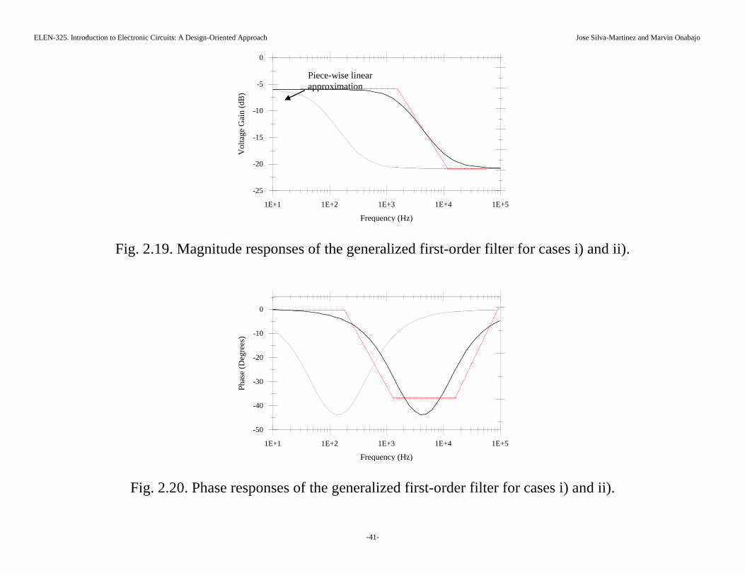
Piecewise linear approximations can be easily plotted for both the magnitude and the phase by following the
rules discussed in previous sections. The magnitude responses in Figure 2.19 and the phase responses in Figure
2.20 represent the following example cases:
i) C1 = 0.159F, C2 = 1.59F, R1 = R2 = 100,
ii) C1 = 0.159F, C2 = 1.59F, R1 = R2 = 4.1k.
In the first case, the DC gain is 1/2 (-6dB) and the high-frequency gain is 0.0909 (-20.8dB). The frequency of
the zero is z = 62.8 krad/sec (fz =10kHz) and the pole is located at p = 11.435 krad/sec (fp = 1.82kHz).
Similarly, the student can easily verify the plots that correspond to the second case.
ELEN-325. Introduction to Electronic Circuits: A Design-Oriented Approach Jose Silva-Martinez and Marvin Onabajo
- - 41
1E+1 1E+2 1E+3 1E+4 1E+5
Frequency (Hz)
-25
-20
-15
-10
-5
0
Volt
age
Gai
n (
dB
)
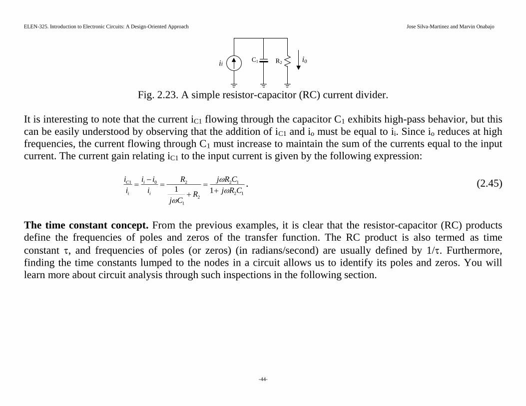
Fig. 2.19. Magnitude responses of the generalized first-order filter for cases i) and ii).
1E+1 1E+2 1E+3 1E+4 1E+5
Frequency (Hz)
-50
-40
-30
-20
-10
0
Phas
e (D
egre
es)
Fig. 2.20. Phase responses of the generalized first-order filter for cases i) and ii).
Piece-wise linear
approximation

ELEN-325. Introduction to Electronic Circuits: A Design-Oriented Approach Jose Silva-Martinez and Marvin Onabajo
- - 42
The current divider. Many important integrated circuit realizations are based on the relationships between
input and output currents because the signals at the device terminals are currents or are easily expressed as such
(e.g., at the collector of a bipolar junction transistor). The basic structure of the current divider is visualized in
Figure 2.21.
Z2ii i0Z1 i1
Fig. 2.21. Current divider.
Here, the problem is to find the output current i0 as function of the input current signal ii and the associated
impedances. Certainly, the output current depends on the relationship between the impedances Z1 and Z2.
Conventional circuit analysis techniques allow us to find the current gain:
21
1
ZZ
Z
i
i
i
o
. (2.43a)
The current flowing through Z2 increases with increment of Z1 or decrement of Z2. Here, it is important to note
that most of the current flows through the smaller impedance. Remember that the relation ii = i1 + i2 must hold at
the summing node; hence, if more current flows through one of the impedances, then less current flows through
the other one such that the addition remains equal to the input current. A similarity with the voltage divider is
that the current gain is a function of the relative values of the impedances rather than the absolute values of the
impedances, as clarified in the following rearranged expression:

ELEN-325. Introduction to Electronic Circuits: A Design-Oriented Approach Jose Silva-Martinez and Marvin Onabajo
- - 43
121
1
ZZi
i
i
o
. (2.43b)
For a resistive current divider (Z1 = R1, Z2 = R2), it can be observed that the output current is significantly
reduced if R2 >> R1, since most of the incoming current under this condition flows through the smaller
impedance (R1), and very little current is collected at the output. On the other hand, most of the current flows
through R2 if R2 << R1.
Similar to the voltage divider, the current transfer function of the current divider becomes a frequency-
dependent complex function in the case where its impedance elements are combinations of resistors and
capacitors. A low-pass transfer function is obtained if the configuration shown in Figure 2.23 is constructed.
Using Eq. 2.43, it follows that
12
12
2
1
1
1
1
1
1
CRs
CR
RCj
Cj
i
i
i
o
. (2.44)
At low frequencies, the capacitive impedance is much higher than R2, and most of the current flows through the
resistor. Consequently, the current gain is close to unity. At = 1/R2C1 (when R2 = |1/jC1|) the magnitude of
the current gain is equal to 1/21/2, and for higher frequencies the current gain reduces inversely proportional to
. This structure is useful for the analysis of multistage current-mode amplifiers. The magnitude and phase
plots of the current gain are similar to the ones obtained for the voltage divider and are not shown here, but we
encourage you to sketch them with piecewise linear approximations as well as plot them with a software
program.
ELEN-325. Introduction to Electronic Circuits: A Design-Oriented Approach Jose Silva-Martinez and Marvin Onabajo
- - 44
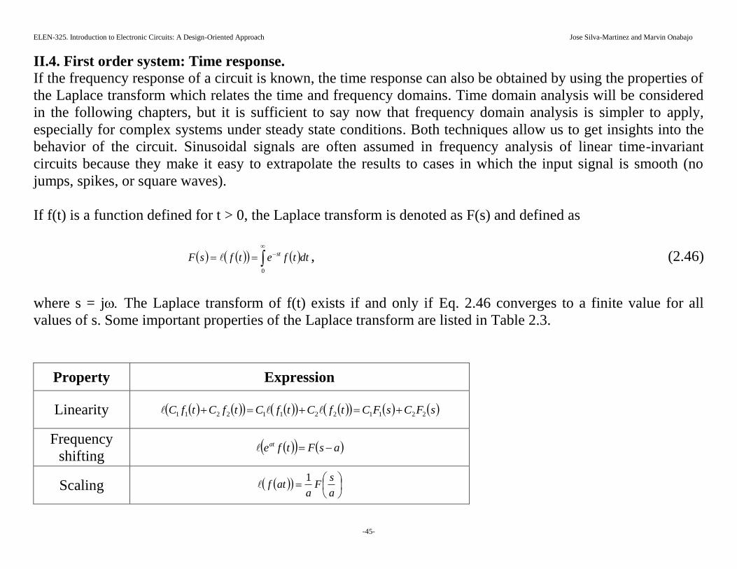
iii0R2
C1
Fig. 2.23. A simple resistor-capacitor (RC) current divider.
It is interesting to note that the current iC1 flowing through the capacitor C1 exhibits high-pass behavior, but this
can be easily understood by observing that the addition of iC1 and io must be equal to ii. Since io reduces at high
frequencies, the current flowing through C1 must increase to maintain the sum of the currents equal to the input
current. The current gain relating iC1 to the input current is given by the following expression:
12
12
2
1
201
11 CRj
CRj
RCj
R
i
ii
i
i
i
i
i
C
. (2.45)
The time constant concept. From the previous examples, it is clear that the resistor-capacitor (RC) products
define the frequencies of poles and zeros of the transfer function. The RC product is also termed as time
constant , and frequencies of poles (or zeros) (in radians/second) are usually defined by 1/. Furthermore,
finding the time constants lumped to the nodes in a circuit allows us to identify its poles and zeros. You will
learn more about circuit analysis through such inspections in the following section.
ELEN-325. Introduction to Electronic Circuits: A Design-Oriented Approach Jose Silva-Martinez and Marvin Onabajo
- - 45
II.4. First order system: Time response.
If the frequency response of a circuit is known, the time response can also be obtained by using the properties of
the Laplace transform which relates the time and frequency domains. Time domain analysis will be considered
in the following chapters, but it is sufficient to say now that frequency domain analysis is simpler to apply,
especially for complex systems under steady state conditions. Both techniques allow us to get insights into the
behavior of the circuit. Sinusoidal signals are often assumed in frequency analysis of linear time-invariant
circuits because they make it easy to extrapolate the results to cases in which the input signal is smooth (no
jumps, spikes, or square waves).
If f(t) is a function defined for t > 0, the Laplace transform is denoted as F(s) and defined as
0
dttfetfsF st , (2.46)
where s = j The Laplace transform of f(t) exists if and only if Eq. 2.46 converges to a finite value for all
values of s. Some important properties of the Laplace transform are listed in Table 2.3.
Property Expression
Linearity sFCsFCtfCtfCtfCtfC 221122112211
Frequency
shifting asFtfeat
Scaling
a
sF
aatf
1
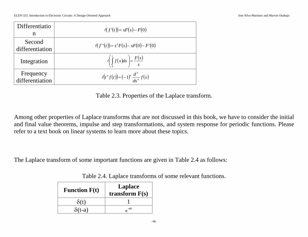
ELEN-325. Introduction to Electronic Circuits: A Design-Oriented Approach Jose Silva-Martinez and Marvin Onabajo
- - 46
Differentiatio
n 0' FssFtf
Second
differentiation 0'0'' 2 FsFsFstf
Integration s
sFdxxf
t
0
Frequency
differentiation sf
ds
dtft
n
nnn 1
Table 2.3. Properties of the Laplace transform.
Among other properties of Laplace transforms that are not discussed in this book, we have to consider the initial
and final value theorems, impulse and step transformations, and system response for periodic functions. Please
refer to a text book on linear systems to learn more about these topics.
The Laplace transform of some important functions are given in Table 2.4 as follows:
Table 2.4. Laplace transforms of some relevant functions.
Function F(t) Laplace
transform F(s)
(t) 1
(t-a) -ase

ELEN-325. Introduction to Electronic Circuits: A Design-Oriented Approach Jose Silva-Martinez and Marvin Onabajo
- - 47
u(t-a) s
e-as
1 , t ≥ 0 (unit
step) s
1
tn-1/(n-1)! ns
1
tn-1∙eat/(n-1)! nas
1
ab
eeatbt
bsas
1
, a b
ab
eaeb atbt
bsas
s
, a b
To illustrate the relationship between the time domain analysis and the s-domain transfer function, let us
consider the following s-domain transfer function:
01
1
1
01
1
1
....
....
bsbsbs
asasas
sv
svn
n
n
m
m
m
i
o
. (2.47)
As illustrated in Figure 2.24 for a first-order system, any system can be characterized in the frequency domain
by noting the magnitude and phase of the input and output signals at different frequencies to obtain its transfer
function H(). Alternatively, the characterization can be performed by determining the transient impulse
response of the circuit; i.e., by applying vi(t) = (t) and finding vo(t) = h(t)∙(t), where h(t) = ℓ-1H(). In general,
the system response to any input signal can be obtained by calculating the convolution of the impulse response
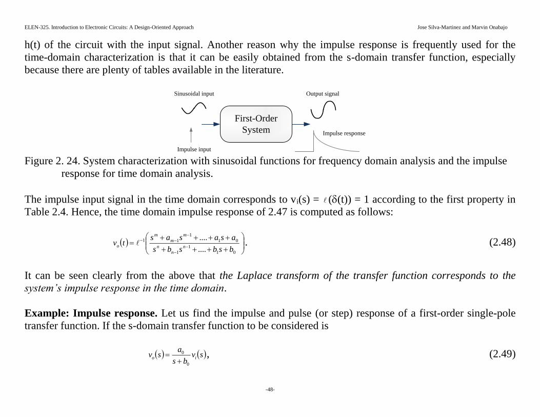
ELEN-325. Introduction to Electronic Circuits: A Design-Oriented Approach Jose Silva-Martinez and Marvin Onabajo
- - 48
h(t) of the circuit with the input signal. Another reason why the impulse response is frequently used for the
time-domain characterization is that it can be easily obtained from the s-domain transfer function, especially
because there are plenty of tables available in the literature.
Impulse input
First-Order
System Impulse response
Sinusoidal input Output signal
Figure 2. 24. System characterization with sinusoidal functions for frequency domain analysis and the impulse
response for time domain analysis.
The impulse input signal in the time domain corresponds to vi(s) = ((t)) = 1 according to the first property in
Table 2.4. Hence, the time domain impulse response of 2.47 is computed as follows:
01
1
1
01
1
11
....
....
bsbsbs
asasastv
n
n
n
m
m
m
o . (2.48)
It can be seen clearly from the above that the Laplace transform of the transfer function corresponds to the
system’s impulse response in the time domain.
Example: Impulse response. Let us find the impulse and pulse (or step) response of a first-order single-pole
transfer function. If the s-domain transfer function to be considered is
svbs
asv io
0
0
, (2.49)

ELEN-325. Introduction to Electronic Circuits: A Design-Oriented Approach Jose Silva-Martinez and Marvin Onabajo
- - 49
then the impulse response is obtained by finding the inverse Laplace transform of this equation. From Table 2.4
and the linearity property, it follows that the impulse response (with vi(s) = 1) of the system is
tb
o eabs
atv 0
0
0
01
. (2.50)
This expression corresponds to the typical exponential function that results from the analytical solution of a
first-order systems, as in the case of a single resistor-capacitor combination for example. The magnitude
response of the first-order filter is displayed in Figure 2.25a. Its DC gain is given by a0/b0, while the -3dB
frequency is determined by b0. The corresponding unit impulse response is shown in Figure 2.25b, where =
1/b0 is the time constant of the first-order system.
3 dB
b0
(log)
20·log10(a0/b0)
Time (Secs)
~0.018
v0 (t)
~0.37~0.13
~0.05
~0.007
1
(a)
(b)
Fig. 2.25 A first-order low-pass system: a) Magnitude response, b) unit impulse response with = 1/b0.
In the previous analysis, it has been assumed that the initial conditions of the system are zero such that v0(0) =
0. When an impulse is applied at the input, the steady state of the system is disturbed, and the output voltage
jumps to the amplitude of the input impulse, which is 1 in this example. The system returns back to its steady
state by exhibiting an exponentially decaying behavior. The system’s time constant time (= 1/b0) is dictated by
the pole frequency b0. After one time constant (at t = the output response has decayed 63%, and it will
continue to decay to 87% of its original value at t = 2= 2/b0 seconds. After t = 4 the output is very close to its
ELEN-325. Introduction to Electronic Circuits: A Design-Oriented Approach Jose Silva-Martinez and Marvin Onabajo
- - 50
final value and the deviation from the steady state value is less than 2%. Settling errors below 1% are acceptable
for many applications. Hence, it takes at least five time constants after the impulse has been applied before the
system returns back to its steady state based on the 1% settling criterion. In the particular case, the steady state
was defined with zero input voltage, but you should be aware that systems can also be characterized when the
DC input and steady state output are non-zero prior to applying the impulse response.
Example: Step response. The step response of a linear system can easily be derived from the impulse response
by using the integration property in Table 2.3. Since the step function in the s-domain corresponds to 1/s in the
frequency response, the time domain output response of the system described by Eq. 2.49 to a unit input step
yields
)0()1()( 0
0
0
0
ostep
tb
t
impulseostepo vVeb
adttvtv
(2.51)
where vo(t)|impulse is given by Eq. 2.50. Vstep is the amplitude of the applied step, and vo(0) is the initial value of
the output voltage at t = 0. The step response of the circuit also exhibits an exponential behavior. If the initial
conditions are zero, then the final output voltage (value at t = ) is given by (a0/b0)∙Vstep. After one time
constant, the output voltage is around 63% of its final value. As shown in Figure 2.26, the output reaches
around 99.3% of the final value after five time constants. The time to reach 99% of the final value is often
called 1% (error) settling time, and the time required to reach this condition is approximately t = 5= 5/b0.
Thus, fast settling behavior implies small time constants (RC products) or, equivalently, poles at high
frequencies. You should remember that the smaller the RC products are, the faster a system’s response is to
disturbances.

ELEN-325. Introduction to Electronic Circuits: A Design-Oriented Approach Jose Silva-Martinez and Marvin Onabajo
- - 51
Time (Secs)
~0.98
v0 (t)
~0.63
~0.86~0.95
~0.993
Vstep(a0/b0)
Fig. 2.26 Step response of the first-order system defined by Eq. 2.49.
General case. The general transfer function in Eq. 2.47 can be rearranged to
01
1
101
1
1 ........ asasassvbsbsbssv m
m
m
i
n
n
n
o
. (2.52)
Applying the Laplace transform to the above expression and assuming zero initial conditions, we can obtain the
time domain input-output relationship:
tva
dt
tvda
dt
tvda
dt
tvd
tvbdt
tvdb
dt
tvdb
dt
tvd
ii
m
i
m
mm
i
m
oo
n
o
n
nn
o
n
01
1
11
1
1
01
1
11
1
1
...
...
. (2.53)
The time domain output can be obtained by solving this differential equation for a given input. Usually, the
solution of this equation is not trivial. It is a lot easier to solve the circuit in the frequency domain to find the
input-output voltage relationship, and then utilize the inverse Laplace transform to obtain the system’s time
domain response.
ELEN-325. Introduction to Electronic Circuits: A Design-Oriented Approach Jose Silva-Martinez and Marvin Onabajo
- - 52
Example: Transformation of a frequency domain transfer function to determine the impulse response. Find the impulse response of the system described by the following second-order s-domain transfer function:
svjsjs
sv io)1010()1010(
10
. (2.54)
The poles of this function are complex conjugates given by
10102,1
jjsp . (2.55)
After substituting vi(s) = 1 from Eq. 2.54, the impulse response can be obtained by using the transform in Table
2.4 for the second-order function with two different poles. The result is
1221
112
))(( pp
tsts
pp
oss
eek
ssss
ktv
pp
(2.56)
where the constant k is equal to 10. If the poles are complex conjugates as in Eq. 2.55, the system’s output
voltage given by 2.56 becomes
)sin(22
tkej
eeek
j
eektv t
tjtjt
tjtj
o
. (2.57)
After substituting the numerical values, we finally get
)10sin(10 10 tetv t
o . (2.58)
This impulse response corresponds to a decaying sinusoidal function with an oscillating frequency (in radians
per second) determined by the imaginary part of the complex conjugate poles. The amplitude of the sinusoidal
ELEN-325. Introduction to Electronic Circuits: A Design-Oriented Approach Jose Silva-Martinez and Marvin Onabajo
- - 53
function is modulated by an exponential function, for which the factor in the exponent depends on the real part
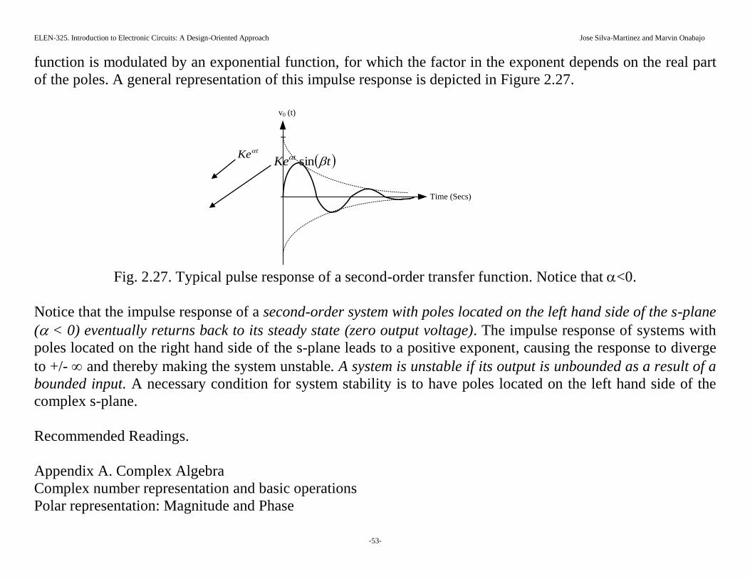
of the poles. A general representation of this impulse response is depicted in Figure 2.27.
Time (Secs)
v0 (t)
Fig. 2.27. Typical pulse response of a second-order transfer function. Notice that <0.
Notice that the impulse response of a second-order system with poles located on the left hand side of the s-plane
(< 0) eventually returns back to its steady state (zero output voltage). The impulse response of systems with
poles located on the right hand side of the s-plane leads to a positive exponent, causing the response to diverge
to +/- and thereby making the system unstable. A system is unstable if its output is unbounded as a result of a
bounded input. A necessary condition for system stability is to have poles located on the left hand side of the
complex s-plane.
Recommended Readings.
Appendix A. Complex Algebra
Complex number representation and basic operations
Polar representation: Magnitude and Phase
tKe
tKe t sin