Chapter 6 Optimizing Power @ Design Time – Interconnect and...
31
Chapter 6 Optimizing Power @ Design Time – Interconnect and Clocks Jan M. Rabaey Optimizing Power @ Design Time Interconnect and Clocks Slide 6.1 So far we have focused our discussion mostly on the energy efficiency of logic. However, interconnect and communication constitute a major component of the overall power budget, as we will demonstrate. They hence deserve some special attention, especially in light of the fact that the physics of interconnect scale some- what differently than those of logic. As with logic, power optimization can again be considered at multiple levels of the design hierarchy. Chapter Outline Trends and bounds An OSI approach to interconnect-optimization – Physical layer – Data link and MAC – Network – Application Clock distribution Slide 6.2 The chapter commences with an analysis of the scal- ing behavior of intercon- nect wires. Some funda- mental bounds on the energy dissipation of inter- connect are established. One particular aspect of this chapter is that it treats on-chip communication as a generic networking pro- blem, and hence classifies the low-energy design tech- niques along the lines of the standard OSI layering (just as we would do for large-scale networking). The chapter concludes with a discussion of one class of wires that need special attention: the clock distribution network. J. Rabaey, Low Power Design Essentials, Series on Integrated Circuits and Systems, DOI 10.1007/978-0-387-71713-5_6, Ó Springer ScienceþBusiness Media, LLC 2009 151
Transcript of Chapter 6 Optimizing Power @ Design Time – Interconnect and...

Chapter 6
Optimizing Power @ Design Time – Interconnect and Clocks
Jan M. Rabaey
Optimizing Power @ Design Time
Interconnect and Clocks
Slide 6.1
So far we have focused ourdiscussion mostly on theenergy efficiency of logic.However, interconnect andcommunication constitutea major component ofthe overall power budget, aswe will demonstrate. Theyhence deserve some specialattention, especially in lightof the fact that the physicsof interconnect scale some-what differently than those
of logic. As with logic, power optimization can again be considered at multiple levels of the designhierarchy.
Chapter Outline
� Trends and bounds
� An OSI approach to interconnect-optimization– Physical layer– Data link and MAC– Network– Application
� Clock distribution
Slide 6.2
The chapter commenceswith an analysis of the scal-ing behavior of intercon-nect wires. Some funda-mental bounds on theenergy dissipation of inter-connect are established.One particular aspect ofthis chapter is that it treatson-chip communication asa generic networking pro-blem, and hence classifiesthe low-energy design tech-niques along the lines of thestandard OSI layering (just
as we would do for large-scale networking). The chapter concludes with a discussion of one class ofwires that need special attention: the clock distribution network.
J. Rabaey, Low Power Design Essentials, Series on Integrated Circuits and Systems,DOI 10.1007/978-0-387-71713-5_6, � Springer ScienceþBusiness Media, LLC 2009
151

ITRS Projections
Calendar Year 2012 2018 2020
Interconnect One Half Pitch 35 nm 18 nm 14 nm
MOSFET Physical Gate Length 14 nm 7 nm 6 nm
Number of Interconnect Levels 12–16
On-Chip Local Clock 20 GHz 53 GHz 73 GHz
Chip-to-Board Clock 15 GHz 56 GHz 89 GHz
# of Hi Perf. ASIC Signal I/O Pads 2500 3100 3100
# of Hi Perf. ASIC Power/Ground Pads 2500 3100 3100
Supply Voltage 0.7–0.9 V 0.5–0.7 V 0.5–0.7 V
Supply Current 283–220 A 396–283 A 396–283 A
14–18 14–18
Slide 6.3
If we consult the ITRSpredictions on how inter-connect will evolve in thecoming decade, weobserve that scaling isprojected to go forwardat the same pace as itdoes today. This leads tosome staggering numbers.By 2020, we may have14–18 (!) layers of inter-connect with the lowestlevels of the interconnectstack at a half pitch ofonly 14 nm. Clocks speeds
could be at multiple tens of GHz, and the number of input and output signals may be largerthan 3000. A simple analysis of what it means to switch this huge interconnect volume leadsto some incredible power numbers. Even aggressive voltage scaling may not be sufficient tokeep the dissipation within bounds. Hence, novel approaches on how to distribute signals ona chip are required.
Increasing Impact of Interconnect
� Interconnect is now exceeding transistors in
– Latency
– Power dissipation
– Manufacturing complexity
� Direct consequence of scaling
Slide 6.4
In fact, the problem isalready with us today. Ifwe evaluate today’s mostadvanced 65 nm deviceswith up to 8 interconnectlayers, multiple hundredsof I/O pins, and clock fre-quencies (at least locally)of up to 5GHz, we seethat providing connectivitybetween the components
poses an essential limitation on the latency levels that can be achieved. It also dominates thepower dissipation � at least, if we also take the clock distribution network into account. Manu-facturing the multiple layers of metal (mostly Cu and Al) and dielectric material in a reliable andpredictable fashion is already a challenge in itself.
Slide 6.5
To drive the point home, this slide shows the power distribution over the different resources for anumber of typical classes of integrated circuits. If I/O, interconnect, and clocks are lumped together,they constitute 50% or more of the budget for each class of devices. The worst case is the FPGA,
152 Chapter #6
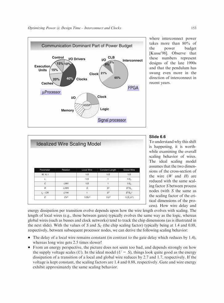
where interconnect powertakes more than 80% ofthe power budget[Kusse’98]. Observe thatthese numbers representdesigns of the late 1990sand that the pendulum hasswung even more in thedirection of interconnect inrecent years.
Idealized Wire Scaling Model
Parameter Relation Local Wire Constant Length Global Wire
W, H, t 1/S 1/S 1/S
L 1/S 1 1/SC
C LW/t 1/S 1 1/SC
R L/WH S S 2 S 2/SC
tp ~ CR L2/Ht 1 S 2 S 2/SC2
E CV 2 1/SU 2 1/U 2 1/(SCU 2)
Slide 6.6
Tounderstandwhy this shiftis happening, it is worth-while examining the overallscaling behavior of wires.The ideal scaling modelassumes that the two dimen-sions of the cross-section ofthe wire (W and H) arereduced with the same scal-ing factor S between processnodes (with S the same asthe scaling factor of the cri-tical dimensions of the pro-cess). How wire delay and
energy dissipation per transition evolve depends upon how the wire length evolves with scaling. Thelength of local wires (e.g., those between gates) typically evolves the same way as the logic, whereasglobal wires (such as busses and clock networks) tend to track the chip dimensions (as is illustrated inthe next slide). With the values of S and SC (the chip scaling factor) typically being at 1.4 and 0.88,respectively, between subsequent processor nodes, we can derive the following scaling behavior:
� The delay of a local wire remains constant (in contrast to the gate delay which reduces by 1.4),whereas long wire gets 2.5 times slower!
� From an energy perspective, the picture does not seem too bad, and depends strongly on howthe supply voltage scales (U). In the ideal model (U = S), things look quite good as the energydissipation of a transition of a local and global wire reduces by 2.7 and 1.7, respectively. If thevoltage is kept constant, the scaling factors are 1.4 and 0.88, respectively. Gate and wire energyexhibit approximately the same scaling behavior.
Communication Dominant Part of Power Budget
65%
21%
9%5%
Interconnect
Clock
I/OCLB
μProcessorClock
LogicMemory
I/O
ASSP
ClocksCaches
Execution Units
Control I/O Drivers
40%20%
15%
15% 10%
FPGA
Signal processor
Optimizing Power @ Design Time – Interconnect and Clocks 153
Unfortunately, the ideal model does not reflect reality. To address the wiring delay challenge,wire dimensions have not been scaled equally. For the layers at the bottom of the interconnectstack, where reducing the wire pitch is essential, wire heights have been kept almost constantbetween technology generations. This increases the cross-section, and hence decreases resistance– which is good for delay reduction. On the other hand, it increases capacitance (and henceenergy) due to the increased contributions of the sidewalls of the wires.
Wires on the top of the stack are not scaled at all. These ‘‘fat’’ wires are used mostly for globalinterconnect. Their capacitance and energy now scales with the chip dimensions – which meansthat they are going up.
An important divergence between logic and interconnect is worth mentioning: though leakagehas become an important component in the energy budget of logic, the same is not true (yet) ininterconnect. The dielectrics used so far have been good enough to keep their leakage undercontrol. This picture may change in the future though.
Distribution of Wire Lengths on Chip
© IEEE 1998
[Ref: J. Davis, C&S’98]
1.0E + 5
1.0E + 4
1.0E + 3
1.0E + 2
1.0E + 1
N – 86161p – 0.8k – 5.0
Inte
rcon
nect
Den
sity
Fun
ctio
n f(
t)
1.0E + 0
1.0E – 11 10
Interconnect Length, Γ[gate pitches]100
Actual DataStochastic Model
1000
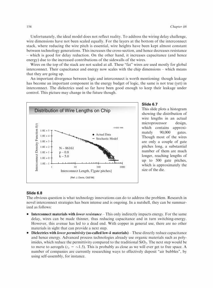
Slide 6.7
This slide plots a histogramshowing the distribution ofwire lengths in an actualmicroprocessor design,which contains approxi-mately 90,000 gates.Though most of the wiresare only a couple of gatepitches long, a substantialnumber of them are muchlonger, reaching lengths ofup to 500 gate pitches,which is approximately thesize of the die.
Slide 6.8
The obvious question is what technology innovations can do to address the problem. Research innovel interconnect strategies has been intense and is ongoing. In a nutshell, they can be summar-ized as follows:
� Interconnect materials with lower resistance – This only indirectly impacts energy. For the samedelay, wires can be made thinner, thus reducing capacitance and in turn switching-energy.However, this avenue has led to a dead end. With copper in general use, there are no othermaterials in sight that can provide a next step.
� Dielectrics with lower permittivity (so-called low-kmaterials) – These directly reduce capacitanceand hence energy. Advanced process technologies already use organic materials such as poly-imides, which reduce the permittivity compared to the traditional SiO2. The next step would beto move to aerogels ("r = �1.5). This is probably as close as we will ever get to free space. Anumber of companies are currently researching ways to effectively deposit ‘‘air bubbles’’, byusing self-assembly, for instance.
154 Chapter #6
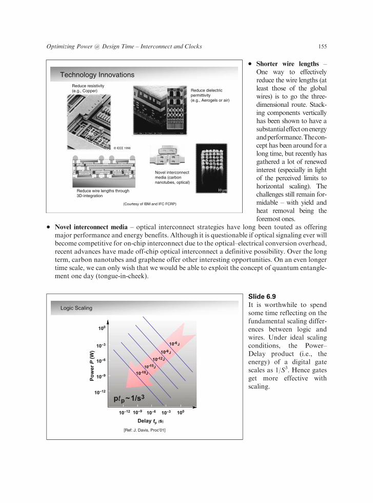
� Shorter wire lengths –One way to effectivelyreduce the wire lengths (atleast those of the globalwires) is to go the three-dimensional route. Stack-ing components verticallyhas been shown to have asubstantialeffectonenergyandperformance.Thecon-cept has been around for along time, but recently hasgathered a lot of renewedinterest (especially in lightof the perceived limits tohorizontal scaling). Thechallenges still remain for-midable – with yield andheat removal being theforemost ones.
� Novel interconnect media – optical interconnect strategies have long been touted as offeringmajor performance and energy benefits. Although it is questionable if optical signaling ever willbecome competitive for on-chip interconnect due to the optical–electrical conversion overhead,recent advances have made off-chip optical interconnect a definitive possibility. Over the longterm, carbon nanotubes and graphene offer other interesting opportunities. On an even longertime scale, we can only wish that we would be able to exploit the concept of quantum entangle-ment one day (tongue-in-cheek).
Logic Scaling
ptp~1/s310–12
10–12
10–9
10–9
10–6
10–6
10–3
10–3
100
100
Pow
er P
(W)
Delay tp (s)
10–6J
10–9J
10–12J
10–15J
10–18J
[Ref: J. Davis, Proc’01]
Slide 6.9
It is worthwhile to spendsome time reflecting on thefundamental scaling differ-ences between logic andwires. Under ideal scalingconditions, the Power–Delay product (i.e., theenergy) of a digital gatescales as 1/S3. Hence gatesget more effective withscaling.
Technology Innovations
Reduce dielectric permittivity (e.g., Aerogels or air)
Reduce resistivity (e.g., Copper)
Reduce wire lengths through 3D-integration
Novel interconnect media (carbon nanotubes, optical)
(Courtesy of IBM and IFC FCRP)
© IEEE 1998
Optimizing Power @ Design Time – Interconnect and Clocks 155
Interconnect Scaling
Delay τ (s)
(Len
gth
)–2 L
–2 (
cm–2
)
Len
gth
L (
cm)
10
10–18 10–3
10–3
10–2
10–2
10–1
10–0100
102
104
106
108
1010
102
10–6
10–5
10–4
10–4
10–910–1210–15
L–2τ = 10–5 [s/cm–2](F = 0.1µ)
L–2τ ~ S 2
10–13
(1000µ)
10–11
(100µ)
10–9(10µ)
10–7(1µ)
[Ref: J. Davis, Proc’01]
Slide 6.10
On the other hand, wirestend to become less effec-tive. For a given technol-ogy, the product of wiredelay andL�2 is a constant,assuming that the delay isdominated by the rc effect.It can hence be consideredto be a figure of merit.Again assuming ideal scal-ing rules (i.e., all dimen-sions scale equally with theexception of the wirelength), �L�2 scales as S2:
�
L2¼ rc ¼ �"
HT/ S2
In other words, the figure of merit of a wire gets worse with technology scaling, at least from aperformance perspective. The only ways to change the scenario is to modify the material char-acteristics (�"), or the propagation mechanism (for instance, by moving from rc-dominateddiffusion to wave propagation).
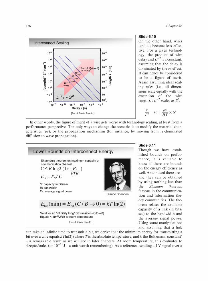
Lower Bounds on Interconnect Energy
Claude Shannon
kTBC ≤ B log2 (1+ PS )
C : capacity in bits/sec B : bandwidth Ps : average signal power
Ebit = PS / C
Valid for an “infinitely long” bit transition (C/B→0)Equals 4.10–21J/bit at room temperature
)2ln()0/((min) kTBCEE bitbit =→=
Shannon’s theorem on maximum capacity of communication channel
[Ref: J. Davis, Proc’01]
Slide 6.11
Though we have estab-lished bounds on perfor-mance, it is valuable toknow if there are boundson the energy efficiency aswell. And indeed there are –and they can be obtainedby using nothing less thanthe Shannon theorem,famous in the communica-tion and information the-ory communities. The the-orem relates the availablecapacity of a link (in bits/sec) to the bandwidth andthe average signal power.Using some manipulationsand assuming that a link
can take an infinite time to transmit a bit, we derive that the minimum energy for transmitting abit over a wire equals kTln(2) (where T is the absolute temperature, and k the Boltzmann constant)– a remarkable result as we will see in later chapters. At room temperature, this evaluates to4 zeptoJoules (or 10�21 J – a unit worth remembering). As a reference, sending a 1V signal over a
156 Chapter #6
1mm intermediate-layer copper wire implemented in a 90 nm technology takes approximately200 fJ, or eight orders of magnitude more than the theoretical minimum.
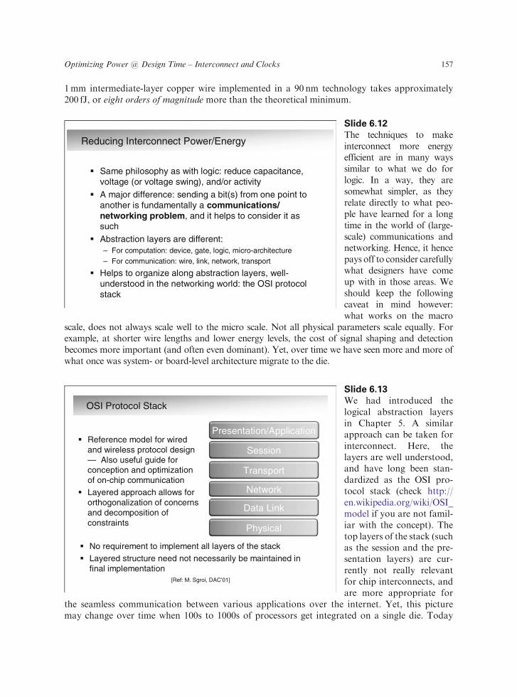
Reducing Interconnect Power/Energy
� Same philosophy as with logic: reduce capacitance, voltage (or voltage swing), and/or activity
� A major difference: sending a bit(s) from one point to another is fundamentally a communications/ networking problem, and it helps to consider it as such
� Abstraction layers are different:– For computation: device, gate, logic, micro-architecture– For communication: wire, link, network, transport
� Helps to organize along abstraction layers, well- understood in the networking world: the OSI protocol stack
Slide 6.12
The techniques to makeinterconnect more energyefficient are in many wayssimilar to what we do forlogic. In a way, they aresomewhat simpler, as theyrelate directly to what peo-ple have learned for a longtime in the world of (large-scale) communications andnetworking. Hence, it hencepays off to consider carefullywhat designers have comeup with in those areas. Weshould keep the followingcaveat in mind however:what works on the macro
scale, does not always scale well to the micro scale. Not all physical parameters scale equally. Forexample, at shorter wire lengths and lower energy levels, the cost of signal shaping and detectionbecomes more important (and often even dominant). Yet, over time we have seen more and more ofwhat once was system- or board-level architecture migrate to the die.
OSI Protocol Stack
� Reference model for wired and wireless protocol design — Also useful guide for conception and optimization of on-chip communication
� Layered approach allows for orthogonalization of concerns and decomposition of constraints
Network
Transport
Session
Data Link
Physical
Presentation/Application
� No requirement to implement all layers of the stack� Layered structure need not necessarily be maintained in
final implementation [Ref: M. Sgroi, DAC’01]
Slide 6.13
We had introduced thelogical abstraction layersin Chapter 5. A similarapproach can be taken forinterconnect. Here, thelayers are well understood,and have long been stan-dardized as the OSI pro-tocol stack (check http://en.wikipedia.org/wiki/OSI_model if you are not famil-iar with the concept). Thetop layers of the stack (suchas the session and the pre-sentation layers) are cur-rently not really relevantfor chip interconnects, andare more appropriate for
the seamless communication between various applications over the internet. Yet, this picturemay change over time when 100s to 1000s of processors get integrated on a single die. Today
Optimizing Power @ Design Time – Interconnect and Clocks 157
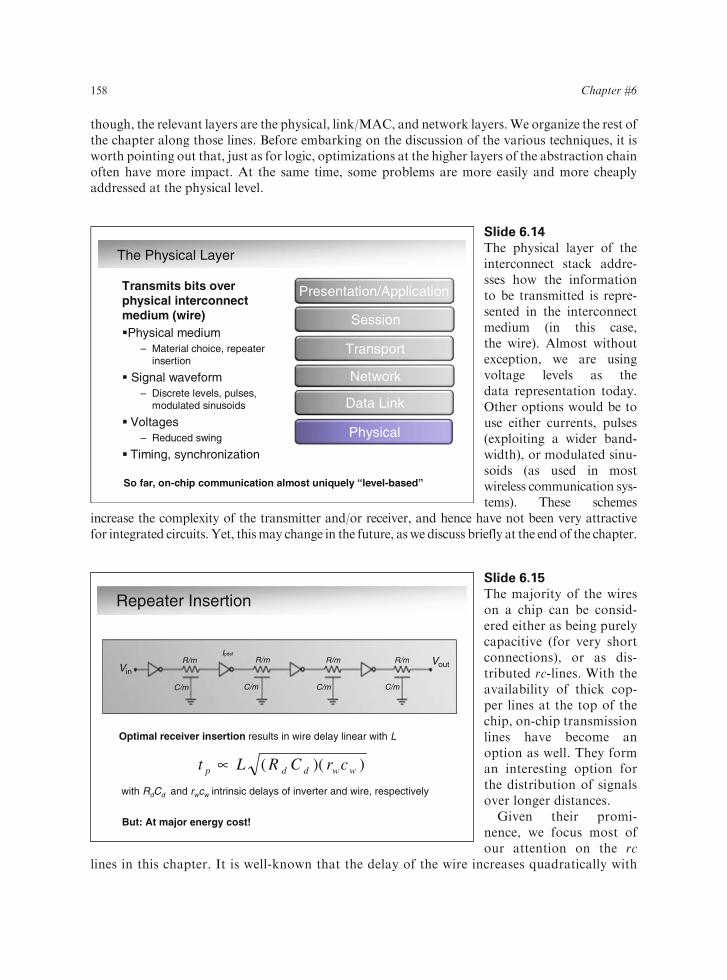
though, the relevant layers are the physical, link/MAC, and network layers.We organize the rest ofthe chapter along those lines. Before embarking on the discussion of the various techniques, it isworth pointing out that, just as for logic, optimizations at the higher layers of the abstraction chainoften have more impact. At the same time, some problems are more easily and more cheaplyaddressed at the physical level.
The Physical Layer
Transmits bits over physical interconnect medium (wire)�Physical medium
– Material choice, repeater insertion
� Signal waveform– Discrete levels, pulses,
modulated sinusoids
� Voltages– Reduced swing
� Timing, synchronization
Network
Transport
Session
Data Link
Physical
Presentation/Application
So far, on-chip communication almost uniquely “level-based”
Slide 6.14
The physical layer of theinterconnect stack addre-sses how the informationto be transmitted is repre-sented in the interconnectmedium (in this case,the wire). Almost withoutexception, we are usingvoltage levels as thedata representation today.Other options would be touse either currents, pulses(exploiting a wider band-width), or modulated sinu-soids (as used in mostwireless communication sys-tems). These schemes
increase the complexity of the transmitter and/or receiver, and hence have not been very attractivefor integrated circuits. Yet, thismay change in the future, as we discuss briefly at the end of the chapter.
Repeater Insertion
Optimal receiver insertion results in wire delay linear with L
))(( wwddp crCRLt ∝with RdCd and rwcw intrinsic delays of inverter and wire, respectively
But: At major energy cost!
VinVout
C/m C/m C/m C/m
R/m R/m R/m R/mIpdef
Slide 6.15
The majority of the wireson a chip can be consid-ered either as being purelycapacitive (for very shortconnections), or as dis-tributed rc-lines. With theavailability of thick cop-per lines at the top of thechip, on-chip transmissionlines have become anoption as well. They forman interesting option forthe distribution of signalsover longer distances.
Given their promi-nence, we focus most ofour attention on the rc
lines in this chapter. It is well-known that the delay of the wire increases quadratically with
158 Chapter #6

its length, whereas the energy dissipation rises linearly. The common technique to get aroundthe delay concern is to insert repeaters at carefully selected intervals, which makes it possible tomake the delay proportional to the length of the wire. The optimal insertion rate (from aperformance perspective) depends upon the intrinsic delays of both the driver and the inter-connect material.
The introduction of repeaters adds active components to an otherwise passive structure, andhence adds extra energy dissipation.
Repeater Insertion ─ Example
� 1 cm Cu wire in 90 nm technology (on intermediate layers)– rw = 250 Ω/mm; cw = 200 fF/mm– tp = 0.69rwcwL2= 3.45 ns
� Optimal driver insertion:– tp opt= 0.5 ns– Requires insertion of 13 repeaters– Energy per transition 8 times larger than just charging
the wire (6 pJ verus 0.75 pJ)!� It pays to back off!
Slide 6.16
The cost of optimal perfor-mance is very high (thisshould be of no surpriseby now). Consider, forinstance, a 1 cm copperline implemented in a90 nm technology. Theenergy cost of the receiveris six times higher thanwhat it takes to just chargethe wire with a single dri-ver. Again, just backingoff a bit from the absoluteminimum delay goes a longway in making the designmore energy-efficient.
Wire Energy–Delay Trade-off
1 2 3 4 5 6 7 80.1
0.2
0.3
0.4
0.5
0.6
0.7
0.8
0.9
1
Eno
rm
Dnorm
wire energy only
L = 1 cm (Cu)90 nm CMOS
(dmin
, emax)
Rep
eate
r ov
erhe
ad
Slide 6.17
As always, the trade-offopportunities are best cap-tured by the energy–delaycurves. Doubling theallowable delay reducesthe required energy by afactor of 5.5! Even justbacking off 10% alreadybuys a 30% energyreduction.
Optimizing Power @ Design Time – Interconnect and Clocks 159

Multi-Dimensional Optimization
� Design parameters:Voltage, number of stages, buffer sizes
� Voltage scaling has thelargest impact, followed by selection of number of repeaters
� Transistor sizing secondary
1 2 3 4 5 6 7 80
2
4
6
8
10
12
Dnorm
Num
ber
of s
tage
s
0.5
0.6
0.7
0.8
0.9
1
1.1
1.2
VD
D(V
)
Slide 6.18
It is worth spending sometime contemplating on howthis pareto-optimal E–Dcurve was obtained. Thedesign parameters involvedinclude the supply (signal)voltage, the number ofstages, and the transistorsizes (in the buffer/repea-ters). From the results ofthe multi-dimensional opti-mization, it can be seen thatthe supply voltage has thebiggest impact, followed byinsertion rate of the repea-ters. Observe that the widthof the wire only has a sec-ondary impact on the wiredelay. Once the wire is wideenough to make the contri-
bution of the fringing capacitance or sidewall capacitance ignorable, further increases in the wirewidth do nothing more than raising the energy dissipation, as is illustrated by the equations below.
cw ¼ w � cpp þ cf rw ¼ rsq=w
�w ¼ cpprsq þ cfrsq=w
Reduced Swing
� Ebit = CVDDVswing
� Concerns:– Overhead (area, delay)– Robustness (supply noise, crosstalk, process variations)– Repeaters?
Transmitter (TX) Receiver (RX)
Slide 6.19
With reduction of the sup-ply voltage (or more pre-cisely, the signal swing)proven to be the most effec-tive technique to saveenergy, some contempla-tion on how to accomplishthis effectively is at hand.As we have observed ear-lier, sending a signal alonga wire is a communicationproblem, and it is worthconsidering as such. Acommunication link con-sists of a transmitter (TX),a communication medium,
and a receiver (RX). The generic configuration in CMOS is to have a driver (inverter) as TX, astretch of aluminum or copper wire in between, and another inverter as a receiver.
160 Chapter #6
This changes once we reduce the signal swing. The TX acts as a driver as well as a level down-converter, whereas the RX performs the up-conversion. Though the energy savings are eitherlinear or quadratic, depending upon the operational voltage of the TX, reducing the swing comeswith an overhead in delay (maybe) and complexity (for sure). In addition, it reduces the noisemargins and makes the design more susceptible to interference, noise, and variations. Yet, as wehave learned from the communications community, the benefits of properly conditioning thesignal can be quite substantial.
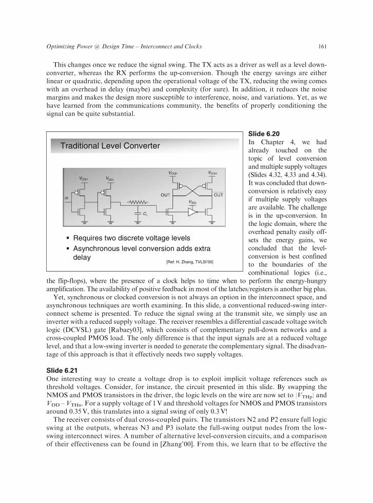
Traditional Level Converter
� Requires two discrete voltage levels
� Asynchronous level conversion adds extra delay
V V
C
V
V
V
[Ref: H. Zhang, TVLSI’00]
Slide 6.20
In Chapter 4, we hadalready touched on thetopic of level conversionandmultiple supply voltages(Slides 4.32, 4.33 and 4.34).It was concluded that down-conversion is relatively easyif multiple supply voltagesare available. The challengeis in the up-conversion. Inthe logic domain, where theoverhead penalty easily off-sets the energy gains, weconcluded that the level-conversion is best confinedto the boundaries of thecombinational logics (i.e.,
the flip-flops), where the presence of a clock helps to time when to perform the energy-hungryamplification. The availability of positive feedback in most of the latches/registers is another big plus.
Yet, synchronous or clocked conversion is not always an option in the interconnect space, andasynchronous techniques are worth examining. In this slide, a conventional reduced-swing inter-connect scheme is presented. To reduce the signal swing at the transmit site, we simply use aninverter with a reduced supply voltage. The receiver resembles a differential cascade voltage switchlogic (DCVSL) gate [Rabaey03], which consists of complementary pull-down networks and across-coupled PMOS load. The only difference is that the input signals are at a reduced voltagelevel, and that a low-swing inverter is needed to generate the complementary signal. The disadvan-tage of this approach is that it effectively needs two supply voltages.
Slide 6.21
One interesting way to create a voltage drop is to exploit implicit voltage references such asthreshold voltages. Consider, for instance, the circuit presented in this slide. By swapping theNMOS and PMOS transistors in the driver, the logic levels on the wire are now set to |VTHp| andVDD – VTHn. For a supply voltage of 1V and threshold voltages for NMOS and PMOS transistorsaround 0.35V, this translates into a signal swing of only 0.3V!
The receiver consists of dual cross-coupled pairs. The transistors N2 and P2 ensure full logicswing at the outputs, whereas N3 and P3 isolate the full-swing output nodes from the low-swing interconnect wires. A number of alternative level-conversion circuits, and a comparisonof their effectiveness can be found in [Zhang’00]. From this, we learn that to be effective the
Optimizing Power @ Design Time – Interconnect and Clocks 161
TX–RX overhead shouldbe no more than 10% ofthe overall energy budgetof the communicationlink.
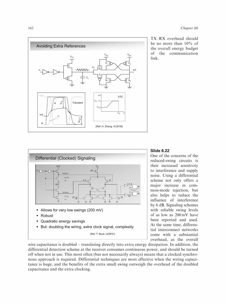
Differential (Clocked) Signaling
� Allows for very low swings (200 mV)� Robust� Quadratic energy savings� But: doubling the wiring, extra clock signal, complexity
CL
CL
[Ref: T. Burd, UCB’01]
Slide 6.22
One of the concerns of thereduced-swing circuits istheir increased sensitivityto interference and supplynoise. Using a differentialscheme not only offers amajor increase in com-mon-mode rejection, butalso helps to reduce theinfluence of interferenceby 6 dB. Signaling schemeswith reliable swing levelsof as low as 200mV havebeen reported and used.At the same time, differen-tial interconnect networkscome with a substantialoverhead, as the overall
wire capacitance is doubled – translating directly into extra energy dissipation. In addition, thedifferential detection scheme at the receiver consumes continuous power, and should be turnedoff when not in use. This most often (but not necessarily always) means that a clocked synchro-nous approach is required. Differential techniques are most effective when the wiring capaci-tance is huge, and the benefits of the extra small swing outweigh the overhead of the doubledcapacitance and the extra clocking.
Avoiding Extra References
Transient
VTC
[Ref: H. Zhang, VLSI’00]In
In2
VT
n
|VT
p|
Out
B
A
in
out
|VTHp|
VDD
VDD - VTn
162 Chapter #6
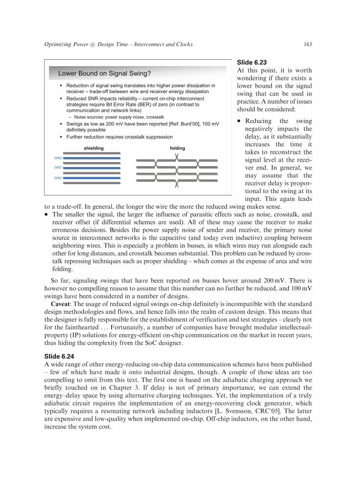
Lower Bound on Signal Swing?
� Reduction of signal swing translates into higher power dissipation in receiver – trade-off between wire and receiver energy dissipation
� Reduced SNR impacts reliability – current on-chip interconnect strategies require Bit Error Rate (BER) of zero (in contrast to communication and network links)– Noise sources: power supply noise, crosstalk
� Swings as low as 200 mV have been reported [Ref: Burd’00], 100 mV definitely possible
� Further reduction requires crosstalk suppression
shielding folding
GND
GND
GND
Slide 6.23
At this point, it is worthwondering if there exists alower bound on the signalswing that can be used inpractice. A number of issuesshould be considered:
� Reducing the swingnegatively impacts thedelay, as it substantiallyincreases the time ittakes to reconstruct thesignal level at the recei-ver end. In general, wemay assume that thereceiver delay is propor-tional to the swing at itsinput. This again leads
to a trade-off. In general, the longer the wire the more the reduced swing makes sense.� The smaller the signal, the larger the influence of parasitic effects such as noise, crosstalk, and
receiver offset (if differential schemes are used). All of these may cause the receiver to makeerroneous decisions. Besides the power supply noise of sender and receiver, the primary noisesource in interconnect networks is the capacitive (and today even inductive) coupling betweenneighboring wires. This is especially a problem in busses, in which wires may run alongside eachother for long distances, and crosstalk becomes substantial. This problem can be reduced by cross-talk repressing techniques such as proper shielding – which comes at the expense of area and wirefolding.
So far, signaling swings that have been reported on busses hover around 200mV. There ishowever no compelling reason to assume that this number can no further be reduced, and 100mVswings have been considered in a number of designs.
Caveat: The usage of reduced signal swings on-chip definitely is incompatible with the standarddesign methodologies and flows, and hence falls into the realm of custom design. This means thatthe designer is fully responsible for the establishment of verification and test strategies – clearly notfor the fainthearted . . . Fortunately, a number of companies have brought modular intellectual-property (IP) solutions for energy-efficient on-chip communication on the market in recent years,thus hiding the complexity from the SoC designer.
Slide 6.24
A wide range of other energy-reducing on-chip data communication schemes have been published– few of which have made it onto industrial designs, though. A couple of those ideas are toocompelling to omit from this text. The first one is based on the adiabatic charging approach webriefly touched on in Chapter 3. If delay is not of primary importance, we can extend theenergy–delay space by using alternative charging techniques. Yet, the implementation of a trulyadiabatic circuit requires the implementation of an energy-recovering clock generator, whichtypically requires a resonating network including inductors [L. Svensson, CRC’05]. The latterare expensive and low-quality when implemented on-chip. Off-chip inductors, on the other hand,increase the system cost.
Optimizing Power @ Design Time – Interconnect and Clocks 163

In this slide, a quasi-adiabatic driver for largecapacitive busses is pre-sented. A stepwise approx-imation of a ramp isproduced by connectingthe output in sequence toa number of evenly distrib-uted voltages, startingfrom the bottom. Fromeach reference, it receives acharge CLV/N before even-tually being connected tothe supply. To dischargethe capacitance, the reversesequence is followed. Foreach cycle, a charge equalto CLV/N is drawn fromthe supply, a reduction by
a factor of N over the single-step charging. The total energy is reduced by the same factor.The N–1 intermediate voltage references are realized using a capacitor tank CTi (where CTi >>
CL). During each charge-and-discharge cycle, each capacitor CTi provides and receives the sameamount of charge, so the tank capacitor voltages are self-sustaining. Even more, it can be shownthat during the start-up, the tank voltages automatically converge to an equal distribution.
In essence, this driver is not truly adiabatic. It rather belongs to the class of the ‘‘charge-redistribution’’ circuits: each cycle, a charge packet is injected from the supply, which thengradually makes its way from level to level during subsequent cycles, and is finally dumped intoground after N cycles. The following slide shows another circuit of the same class.
Charge Redistribution Schemes
VDD/2
VDD/4
3VDD/4
Precharge Eval Precharge
B0
B0
B1
B1
B0 = 0
B1 = 1
VDD
E
E
E
P
P
GND
RX1
RX0
1
0
B1
B1
B0
B0
� Charge recycled from top to bottom� Precharge phase equalizes differential lines� Energy/bit = 2C(VDD/n)2
� Challenges: Receiver design, noise margins[Ref: H. Yamauchi, JSSC’95]
Slide 6.25
‘‘Charge recycling’’ is another idea that is very intri-guing, but has rarely beenused. In a traditionalCMOS scheme, charge isused only a single time: itis transferred from the sup-ply to the load capacitor ina first phase, and dumpedto the ground in a second.From an energy perspec-tive, it would be great if wecould use charge a coupleof times before dumpingit. This by necessityrequires the use of multiplevoltage levels. A simplifiedexample of a chargerecy-
cling bus with two levels is shown in this slide. Each bit i is present in differential form
Quasi-Adiabatic Charging
t
V VDD
VDD/n
• Uses stepwise approximation of adiabatic (dis)charging• Capacitors acting as “charge reservoir”• Energy drawn from supply reduced by factor n
CT1
CT2
CTn–1
CT1 CL
CT2
CTn-1
[Ref: L. Svensson, ISLPED’96]
164 Chapter #6

ðBi and BiÞ. During the precharge phase, the two differential lines for each bit are equalized byclosing the switches P. During evaluation, one of the lines is connected to a line of a ‘‘higher-order’’bit (representing a 1), whereas the other is equalized with a ‘‘lower-order’’ bit (representing a 0)using the switches E. This produces a differential voltage at each line pair, the polarity of whichdepending upon the logic value to be transmitted. Differential amplifiers at the end of the bus (onefor each pair) reproduce the full swing signals.
Assuming that the capacitances of all lines are equal, we can see that the precharge voltage levelsdivide equally between VDD and GND. The signal swing on each bus pair equals VDD/N. Theprinciple is quite similar to that of the quasi-adiabatic driver of the previous slide – a charge packetis injected from the supply, which sequentially drives every bit of the bus in descending order, untileventually being dumped on the ground.
The challenge resides in adequately detecting the various output levels in the presence of processvariations and noise. Yet, the idea has enough potential that it is bound to be useful in a number ofspecial cases.
Alternative Communication Schemes
� Example: Capacitively driven wires
Offers some compelling advantages � Reduced swing
Swing is VDD/(n+1) without extra supply
� Reduced loadAllows for smaller driver
� Reduced delayCapacitor pre-emphasizes edges Pitchfork capacitors exploit
sidewall capacitance
[Ref: D. Hopkins, ISSCC’07]
Slide 6.26
At the end of this discus-sion on physical-layer sig-naling, it is worth pointingout some other signalingstrategies that may becomeattractive. In this slide, weshow only one of them.Rather than connectingresistively into the inter-connect network, driverscould also couple capaci-tively. The net effect is thatthe swing on the intercon-nect wire is reduced auto-matically without needingany extra supplies. In addi-tion, driver sizes can bereduced, and signal transi-
tions are sharper. The approach comes with a lot of challenges as well (one still needs a level-restoring receiver, for instance), but is definitely worth keeping an eye on.
Slide 6.27
So far, we have concentrated on the data representations of our signaling protocol, and have ignoredtiming. Yet, the interconnect network plays an important role in the overall timing strategy of acomplex system-on-a-chip (SoC). To clarify this statement, let us consider the following simpleobservation: It takes an electronic signal moving at its fastest possible speed (assuming transmis-sion-line conditions) approximately 66ps to move from one side to the other of a 1 cm chip. When rc-effects dominate, the reality is a lot worse, as shown in Slide 6.16, where the minimum delay wasdetermined to be 500ps. This means that for clock speeds faster than 2GHz, it takes more than oneclock cycle for a signal to propagate across the chip! The situation is evenworse, when the interconnectwire is loaded with a large distributed fan-out – as is always the case with busses, for instance.
There are a number of ways to deal with this. One commonly used option is to pipeline thewire by inserting a number of clocked buffer elements. This happens quite naturally in the
Optimizing Power @ Design Time – Interconnect and Clocks 165
network-on-a-chip (NoC)paradigm, which we willdiscuss shortly. Yet, allthis complicates the overalltiming of the chip, andintrinsically links the tim-ing of global interconnectand localized computation.This hampers the introduc-tion of a number of powerreduction techniques wehave discussed earlier(such as multiple supplyvoltages and timing relaxa-tion), or to be discussed incoming chapters (such asdynamic voltage and fre-
quency scaling).Hence it makes sense to decouple global interconnect and local compute timing through the use
of asynchronous signaling. Along these lines of thinking, one methodology called GALS (GloballyAsynchronous Locally Synchronous) has attracted a following in recent years [Chapiro’84]. Theidea is to use a synchronous approach for the local modules (called synchronous islands), whilecommunication between them is performed asynchronously. This approach dramatically relaxesthe clock distribution and interconnect timing requirements, and enables various power-savingtechniques for the processor modules.
Signaling Protocols
Network
Physical Layer Interface Module
ProcessorModule
(mProc, ALU, MPY, SRAM…)
din reqin ackindout reqout ackout
din dout clk
din
reqin
clk
done
Locally synchronous
done
Globally asynchronous
Slide 6.28
Asynchronous signalingopens the door for multipleoptimizations. Yet it comeswith the overhead of addingvarious extra control sig-nals such as req(uest)and ack(nowledgement).Although that overheadcan be shared by the Nwires in the bus, it still issubstantial. This is why thetwo-phase signaling proto-col is preferred over themore robust four-phaseprotocol for large-intercon-nect networks [Rabaey’03].
The generation and termination of the control signals is most effectively performed by astandardized wrapper around the computational modules, which serves as the boundary betweenthe synchronous and asynchronous domains. One of the very first designs that followed thatconcept is presented in [Zhang’00].
Signaling Protocols
Network
ProcessorModule
(μProc, ALU, MPY, SRAM…)
din reqin ackin dout req out ackout
Din
done
Globally Asynchronousself-timed handshaking protocol
Allows individual modulesto dynamically trade-off performancefor energy efficiency
166 Chapter #6

The Data Link/Media Access Layer
Reliable transmission over physical link and sharing interconnect medium between multiple sources and destinations (MAC)� Bundling, serialization, packetizing� Error detection and correction� Coding� Multiple-access schemes
Network
Transport
Session
Presentation/Application
Data Link
Physical
Slide 6.29
Whereas the physical layerdeals with the various aspectsofhowtorepresentdataontheinterconnect medium, thefunction of the link layer is toensure that data is reliablytransmitted in the appropriateformats between the sourceandthedestination.Forexam-ple, in the wired and wirelessnetworking world, packets ofdata are extended with someextra error-control bits, whichhelp the destination to deter-mine if thepacketwasnotcor-rupted during its travel.
If the link connects to multiple sources and destinations, the media access control (MAC)protocol ensures that all sources can share the media in a fair and reliable fashion. Bus arbitrationis a great example of a MAC protocol used extensively in SoCs.
Most designers still consider interconnect purely as a set of wires. Yet, thinking aboutthem as a communication network opens the door for a broad range of opportunities, thescope of which will only increase with further scaling. As a starter, the link layer offers agreat number of means of introducing energy-saving techniques for global interconnects. Forexample, adding error-correcting coding allows for a more aggressive scaling of the voltagelevels used in a bus.
Coding
N N + k N
LinkTX RX
Adding redundancy to communication link (extra bits) to:� Reduce transitions (activity encoding)� Reduce energy/bit (error-correcting coding)
Slide 6.30
Coding is a powerful tech-nique, which is extensivelyused in most wired andwireless communicationsystems. So far, its over-head has been too high tobe useful in on-chip inter-connects. With the growingcomplexity of integratedcircuits, this may rapidlybe changing. A number ofcoding strategies can beconsidered:
� Channel-coding techni-ques, which modify the
data to be transmitted so that it better deals with imperfections of the channel.� Error-correcting codes, which add redundancy to the data so that eventual transmission errors
can be detected and/or corrected.
Optimizing Power @ Design Time – Interconnect and Clocks 167
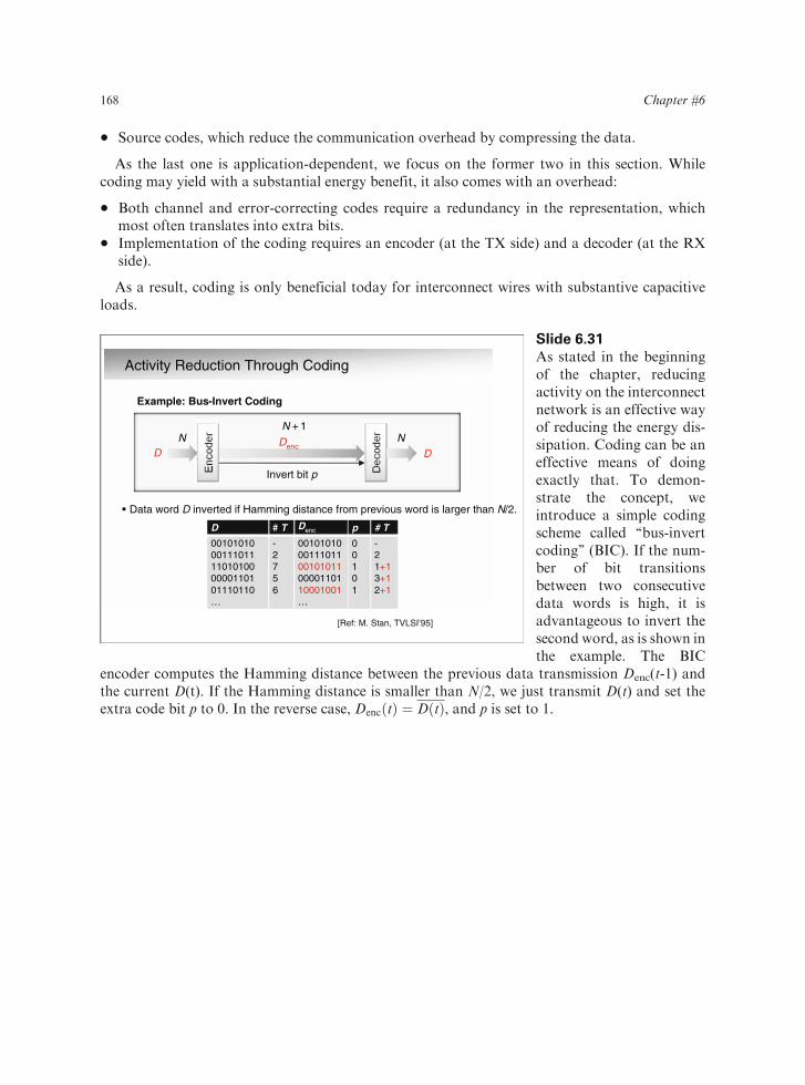
� Source codes, which reduce the communication overhead by compressing the data.
As the last one is application-dependent, we focus on the former two in this section. Whilecoding may yield with a substantial energy benefit, it also comes with an overhead:
� Both channel and error-correcting codes require a redundancy in the representation, whichmost often translates into extra bits.
� Implementation of the coding requires an encoder (at the TX side) and a decoder (at the RXside).
As a result, coding is only beneficial today for interconnect wires with substantive capacitiveloads.
Activity Reduction Through Coding
NN + 1
N
Example: Bus-Invert Coding
Invert bit p
� Data word D inverted if Hamming distance from previous word is larger than N/2.
DDenc
D
D # T Denc p # T
0010101000111011110101000000110101110110…
-2756
0010101000111011001010110000110110001001…
00101
-21+13+12+1
[Ref: M. Stan, TVLSI’95]
Slide 6.31
As stated in the beginningof the chapter, reducingactivity on the interconnectnetwork is an effective wayof reducing the energy dis-sipation. Coding can be aneffective means of doingexactly that. To demon-strate the concept, weintroduce a simple codingscheme called ‘‘bus-invertcoding’’ (BIC). If the num-ber of bit transitionsbetween two consecutivedata words is high, it isadvantageous to invert thesecond word, as is shown inthe example. The BIC
encoder computes the Hamming distance between the previous data transmission Denc(t-1) andthe current D(t). If the Hamming distance is smaller than N/2, we just transmit D(t) and set theextra code bit p to 0. In the reverse case, DencðtÞ ¼ DðtÞ, and p is set to 1.
168 Chapter #6
Bus-Invert Coding
Gain:25 % (at best – for random data)
Overhead: Extra wire (and activity)Encoder, decoder
Not effective for correlated data
Gain:25% (at best – for random data)
Overhead: Extra wire (and activity)Encoder, decoder
Not effective for correlated data
P
Encode
Decode
D DDenc
p
Bus
[Ref: M. Stan, TVLSI’95]
Slide 6.32
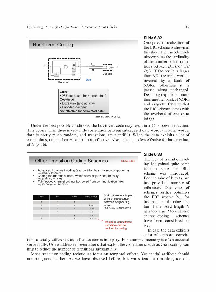
One possible realization ofthe BIC scheme is shown inthis slide. The Encode mod-ule computes the cardinalityof the number of bit transi-tions between Denc(t-1) andD(t). If the result is largerthan N/2, the input word isinverted by a bank ofXORs, otherwise it ispassed along unchanged.Decoding requires no morethan another bank ofXORsand a register. Observe thatthe BIC scheme comes withthe overhead of one extrabit (p).
Under the best possible conditions, the bus-invert code may result in a 25% power reduction.This occurs when there is very little correlation between subsequent data words (in other words,data is pretty much random, and transitions are plentiful). When the data exhibits a lot ofcorrelations, other schemes can be more effective. Also, the code is less effective for larger valuesof N (> 16).
Other Transition Coding Schemes
Advanced bus-invert coding (e.g. partition bus into sub-components) (e.g. [M.Stan, TVLSI’97])
Coding for address busses (which often display sequentiality) (e.g. [L. Benini, DATE’98])
Full-fledged channel coding, borrowed from communication links (e.g. [S. Ramprasad, TVLSI’99])
Coding to reduce impact of Miller capacitance between neighboring wires [Ref: Sotiriadis, ASPDAC’01]
Maximum capacitance transition – can be avoided by coding
bit k-1 bitk bit k+1 Delay factor g
1
− 1 + r
1 + 2r
− − 1 + 2r
− 1 + 3r
1 + 4r
Slide 6.33
Slide 6.33
The idea of transition cod-ing has gained quite sometraction since the BICscheme was introduced.For the sake of brevity, wejust provide a number ofreferences. One class ofschemes further optimizesthe BIC scheme by, forinstance, partitioning thebus if the word length Ngets too large. More genericchannel-coding schemeshave been considered aswell.
In case the data exhibitsa lot of temporal correla-
tion, a totally different class of codes comes into play. For example, memory is often accessedsequentially. Using address representations that exploit the correlations, such as Gray coding, canhelp to reduce the number of transitions substantially.
Most transition-coding techniques focus on temporal effects. Yet spatial artifacts shouldnot be ignored either. As we have observed before, bus wires tend to run alongside one
Optimizing Power @ Design Time – Interconnect and Clocks 169
another for long distances. The intra-wire capacitance can hence be as or even moreimportant than the capacitance to ground. Under unfavorable conditions, as the table onthe slide indicates, a wire can experience a capacitance that is many times larger than themost favorable case. Codes can be engineered to minimize the occurrence of ‘‘aggressions’’between neighboring bits. Their overhead is manageable as well, as was established in[Sotiriades’01].
++
Error-Correcting Codes
NN + k
ND
DencD
with
e.g.,
1
1
0
= 3
Example: (4,3,1) Hamming Code
B 3wrong Adding redundancy allows
for more aggressive scaling of signal swings and/or timing
Simpler codes such as Hamming prove most
Adding redundancy allows for more aggressive scaling of signal swings and/or timing
Simpler codes such as Hamming prove most effective
P1P2B3P4B5B6B7
P1 B3 B5 B 7 = 0
P4 B5 B5 B 7 = 0+
P2 B3 B6 B 7 = 0+
+
+++
+
+
+++
+
+
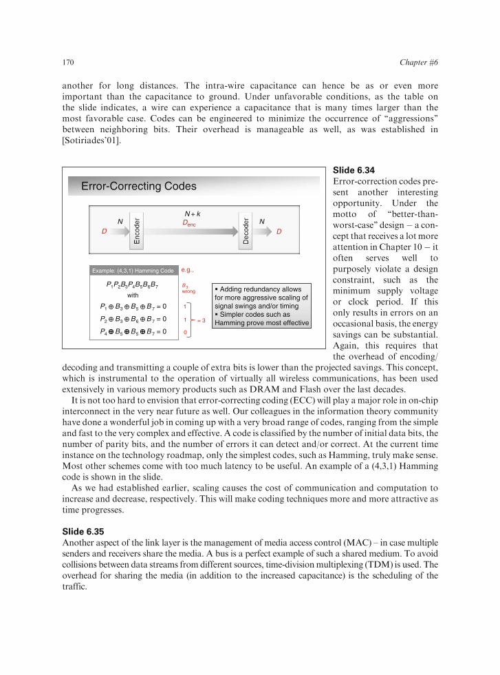
Slide 6.34
Error-correction codes pre-sent another interestingopportunity. Under themotto of ‘‘better-than-worst-case’’ design� a con-cept that receives a lot moreattention in Chapter 10� itoften serves well topurposely violate a designconstraint, such as theminimum supply voltageor clock period. If thisonly results in errors on anoccasional basis, the energysavings can be substantial.Again, this requires thatthe overhead of encoding/
decoding and transmitting a couple of extra bits is lower than the projected savings. This concept,which is instrumental to the operation of virtually all wireless communications, has been usedextensively in various memory products such as DRAM and Flash over the last decades.
It is not too hard to envision that error-correcting coding (ECC) will play amajor role in on-chipinterconnect in the very near future as well. Our colleagues in the information theory communityhave done a wonderful job in coming up with a very broad range of codes, ranging from the simpleand fast to the very complex and effective. A code is classified by the number of initial data bits, thenumber of parity bits, and the number of errors it can detect and/or correct. At the current timeinstance on the technology roadmap, only the simplest codes, such as Hamming, truly make sense.Most other schemes come with too much latency to be useful. An example of a (4,3,1) Hammingcode is shown in the slide.
As we had established earlier, scaling causes the cost of communication and computation toincrease and decrease, respectively. This will make coding techniques more and more attractive astime progresses.
Slide 6.35
Another aspect of the link layer is the management of media access control (MAC) – in case multiplesenders and receivers share the media. A bus is a perfect example of such a shared medium. To avoidcollisions between data streams from different sources, time-divisionmultiplexing (TDM) is used. Theoverhead for sharing the media (in addition to the increased capacitance) is the scheduling of thetraffic.
170 Chapter #6

With an eye on the future,it is again worth ponderingthe possibility of borrowingideas from the wireless-and optical-communicationcommunities that utilize thediversity offered by the fre-quency domain. Today, allIC communications aresituated in the baseband(i.e., from 0Hz to 100s ofMHz), similar to whereoptical communicationsused to be for a long time(before the introduction ofwave-division multiplexingor WDM). Modulation ofsignal streams to a number
of higher-frequency channels allow for the same wire to be used simultaneously by a number ofstreams. The overhead of modulation/demodulation is quite substantial – yet, it is plausible thatfrequency-division multiplexing (FDM) or code-division multiplexing (CDM) techniques may beused in the foreseeable future for high-capacity energy-efficient communication backplanesbetween chips, where the link capacitance is large. A great example of such a strategy is given in[Chang’08].
In light of this, TDM is the only realistic on-chip media-access protocol today. Even here, manydifferent options exist, especially regarding the granting of access to the channel. The simplestoption is for a source to just start transmitting when data is available. The chance for a collisionwith other sources is extremely high though, and the overhead of retransmission attempts dom-inates the energy and latency budgets. The other extreme is to assign each stream its own time slot,granted in advance. This works well for streams that need guaranteed throughput, but may leavesome channels heavily under-utilized. Bus arbitration is the most common scheme: a source withdata available requests the channel, and starts transmitting when access is granted. The overheadof this scheme is in the execution of the ‘‘arbitration’’ protocol.
Media Access
Sharing of physical media over multiple data streams increases capacitance and activity (see Chapter 5), but reduces areaMany multi-access schemes known from communications – Time domain: Time-Division Multiple Access (TDMA)– Frequency domain: narrow band, code division multiplexing
Buses based on Arbitration-based TDMA most common in today’s ICs
Optimizing Power @ Design Time – Interconnect and Clocks 171
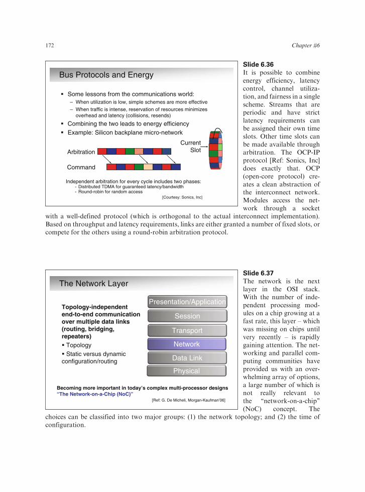
Bus Protocols and Energy
Some lessons from the communications world:– When utilization is low, simple schemes are more effective – When traffic is intense, reservation of resources minimizes
overhead and latency (collisions, resends)
Combining the two leads to energy efficiencyExample: Silicon backplane micro-network
CurrentSlot
Independent arbitration for every cycle includes two phases:- Distributed TDMA for guaranteed latency/bandwidth- Round-robin for random access
Arbitration
Command
[Courtesy: Sonics, Inc]
Slide 6.36
It is possible to combineenergy efficiency, latencycontrol, channel utiliza-tion, and fairness in a singlescheme. Streams that areperiodic and have strictlatency requirements canbe assigned their own timeslots. Other time slots canbe made available througharbitration. The OCP-IPprotocol [Ref: Sonics, Inc]does exactly that. OCP(open-core protocol) cre-ates a clean abstraction ofthe interconnect network.Modules access the net-work through a socket
with a well-defined protocol (which is orthogonal to the actual interconnect implementation).Based on throughput and latency requirements, links are either granted a number of fixed slots, orcompete for the others using a round-robin arbitration protocol.
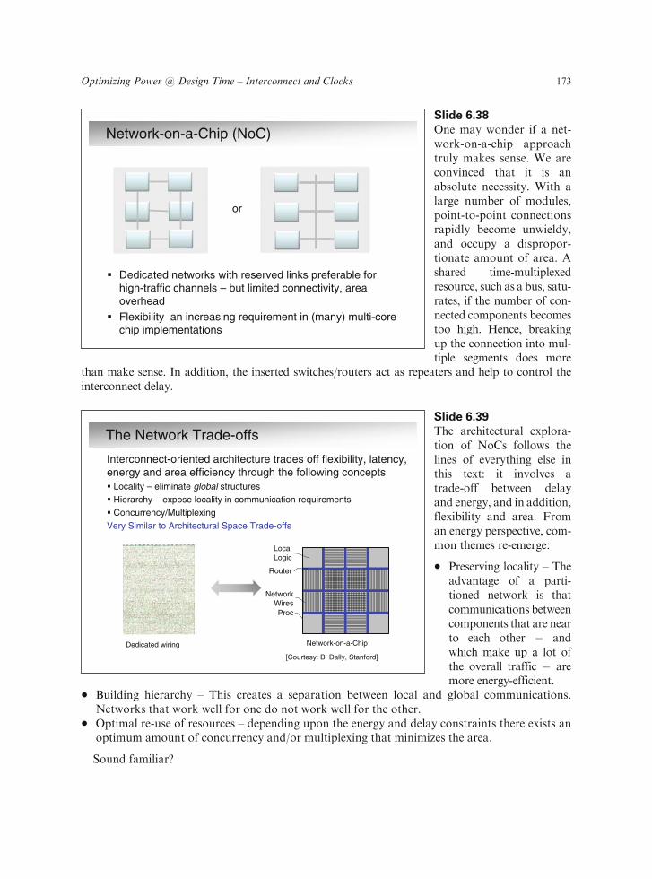
The Network Layer
Topology-independent end-to-end communication over multiple data links (routing, bridging, repeaters) Topology Static versus dynamic
configuration/routing
Physical
Transport
Session
Data Link
Network
Presentation/Application
Becoming more important in today’s complex multi-processor designs“The Network-on-a-Chip (NoC)”
[Ref: G. De Micheli, Morgan-Kaufman’06]
Slide 6.37
The network is the nextlayer in the OSI stack.With the number of inde-pendent processing mod-ules on a chip growing at afast rate, this layer – whichwas missing on chips untilvery recently – is rapidlygaining attention. The net-working and parallel com-puting communities haveprovided us with an over-whelming array of options,a large number of which isnot really relevant tothe ‘‘network-on-a-chip’’(NoC) concept. The
choices can be classified into two major groups: (1) the network topology; and (2) the time ofconfiguration.
172 Chapter #6
Network-on-a-Chip (NoC)
Dedicated networks with reserved links preferable for high-traffic channels – but limited connectivity, area overheadFlexibility an increasing requirement in (many) multi-corechip implementations
or
Slide 6.38
One may wonder if a net-work-on-a-chip approachtruly makes sense. We areconvinced that it is anabsolute necessity. With alarge number of modules,point-to-point connectionsrapidly become unwieldy,and occupy a dispropor-tionate amount of area. Ashared time-multiplexedresource, such as a bus, satu-rates, if the number of con-nected components becomestoo high. Hence, breakingup the connection into mul-tiple segments does more
than make sense. In addition, the inserted switches/routers act as repeaters and help to control theinterconnect delay.
The Network Trade-offs
Interconnect-oriented architecture trades off flexibility, latency, energy and area efficiency through the following concepts
Locality – eliminate global structuresHierarchy – expose locality in communication requirementsConcurrency/Multiplexing
Very Similar to Architectural Space Trade-offs
Dedicated wiring Network-on-a-Chip
LocalLogic
Router
Proc
NetworkWires
[Courtesy: B. Dally, Stanford]
Slide 6.39
The architectural explora-tion of NoCs follows thelines of everything else inthis text: it involves atrade-off between delayand energy, and in addition,flexibility and area. Froman energy perspective, com-mon themes re-emerge:
� Preserving locality – Theadvantage of a parti-tioned network is thatcommunications betweencomponents that are nearto each other � andwhich make up a lot ofthe overall traffic � aremore energy-efficient.
� Building hierarchy – This creates a separation between local and global communications.Networks that work well for one do not work well for the other.
� Optimal re-use of resources – depending upon the energy and delay constraints there exists anoptimum amount of concurrency and/or multiplexing that minimizes the area.
Sound familiar?
Optimizing Power @ Design Time – Interconnect and Clocks 173

Networking Topologies
Homogeneous– Crossbar, Butterfly, Torus, Mesh,Tree, …
Heterogeneous– Hierarchy
Mesh (FPGA)
Tree
Crossbar
FF
FF
FF
FF
Slide 6.40
We could spend a lot of valu-able book ‘‘real estate’’ on anoverview of all the possibleinterconnect topologies thatare known to mankind, butmuch of it would be wasted.For instance, a number ofstructures that excel in high-performance parallel compu-ters do not map well on thetwo-dimensional surface ofan integrated circuit; anexample of such is the hypercube. We therefore restrictour discussion to the topolo-gies that are commonly usedon-chip.
� The crossbar presents alatency-efficient way of connecting n sources tom destinations. However, it is expensive from bothan area and energy perspective.� The mesh is the most popular NoC architecture today. The FPGA was the first chip family to
adopt this topology. The advantage of the mesh is that it uses only nearest-neighbor connec-tions, thus preserving locality when necessary. For long-distance connections, the multi-hopnature of the mesh leads to large latencies. To combat this effect, FPGAs overlay meshes withdifferent granularity.
� A binary tree network realizes a log2(N) latency network (where N is the number of elements inthe network) with relatively low wiring and capacitance costs. Other versions of this networkvary the cardinality of the tree. In a fat tree, the cardinality is gradually increased for the higherlevels. Trees offer an interesting counterpart to meshes as they are more effective in establishinglong-distance connectivity.
Given that each network topology has its strengths and weaknesses, it comes as no surprise thatmany of the deployed NoCs pragmatically combine a number of schemes in a hierarchical fashion,presenting one solution for local wiring supplemented by another for the global connections. Inaddition, point-to-point connections are used whenever needed.
Slide 6.41
Navigating the myriad choices in an educated fashion once again requires an exploration environ-ment that allows a study of the trade-off between the relevant metrics over the parameter set.
This is illustrated by the example in this slide, which compares the mesh and binary treenetworks in the energy–delay space. As can be expected, the mesh network is the mosteffective solution for short connections, whereas the tree is the preferred choice for thelonger ones. A solution that combines the two networks leads to a network with a mergedpareto-optimal curve.
This combination is not entirely effective. If the goal is to make the latency between any twomodules approximately uniform, straightforwardly combining the tree and the mesh topologies
174 Chapter #6

helps somewhat, but longerconnections are still expen-sive. It would be better ifthe lower levels of the treespan nodes that are furtheraway from each other, asshown in the lower dia-gram, picturing an‘‘inverted-clustering’’ tree.The combination of themesh with the inverse-clus-tering tree provides asuperior solution, whichonly rises slightly with theManhattan distancebetween the nodes.
Circuit-Switched Versus Packet-Based
On-chip reality : Wires (bandwidth) are relatively cheap; buffering and routing expensivePacket-switched approach versatile– Preferred approach in large networks
– But … routers come with large overhead– Case study Intel: 18% of power in link, 82%
in router
Circuit-switched approach attractive for high-data-rate quasi-static linksHierarchical combination often preferred choice
BusBus
C C
C C
Bus to connect over short distances
Hierarchical circuit- and packet-switched networks for longer connections
Bus
C C
C C
Bus
C C
C C
Bus
C C
C C
Bus
C C
C C
R R
R R
Bus Bus
Bus Bus
Slide 6.42
The other importantdimension in the networkexploration is the choiceof the routing strategy,and the time at which itis established. The staticrouting is the simplestoption. In this case, net-work routes are set up atdesign time. This is, forinstance, the case in FPGAs,where the switches in theinterconnect network are setat design time. A simplemodification of this is toenable reconfiguration. Thisallows for a route to be set upfor a time (for instance, for
the duration of a computational task), and then be ripped up and rerouted. This approach resembles thecircuit-switched approach of the traditional telephone networks. The advantage of both static- andcircuit-switched routing is that the overhead is reasonable and solely attributable to the additionalswitches in the routing paths. (Note: for performance reasons, these switches are often made quitelarge and add a sizable amount of capacitance).
Packet-switched networks present a more flexible solution, where routes are chosen on a per-packet basis (as is done in some of the Internet routers). The overhead for this is large, as eachrouter element has to support buffering as well as dynamic route selection. Amajor improvement is
Network Topology Exploration
Manhattan Distance
Ene
rgy
x D
elay
Mesh
Binary Tree
Manhattan Distance
Ene
rgy
x D
elay
Mesh
Binary Tree
Mesh + Inverse-clustering tree
Short connections in tree are redundant
Inverse clustering complements mesh
[Ref: V. George, Springer’01]
Optimizing Power @ Design Time – Interconnect and Clocks 175

inspired by the realization that most data communications consist of a train of sequential packets.Under those conditions, the routing decision can be made once (for the first packet), with the otherpackets in the train just following. This approach is called ‘‘flit-routing’’ [Ref: Dally’01].
Experiments have shown that flit routing in NoCs is still quite expensive and that the energy costof the dynamic routing is multiple times higher than the cost of the link. This realization is quiteessential: the energy cost of transmitting a bit over a wire on a chip is still quite reasonable comparedto the implementation cost of routers and buffers. As long as this is the case, purely dynamic networkstrategies may not be that attractive. Heterogeneous topologies, such as combining busses for shortconnections with mesh- or tree-based circuit- or packet-switched networks for the long-distanceones, most probably offer a better solution.
Example: The Pleiades Network-on-a-Chip
Configuration Bus• Configurable platform for low-energy communication and signal-processing applications (see Chapter 5)• Allows for dynamic task-level reconfiguration of process networks
Energy-efficient flexible network essential to the concept
Configurable Interconnect
ArithmeticModule
ArithmeticModule
ArithmeticModule
ConfigurableLogic
ConfigurableLogicμPμP
Configuration
DedicatedArithmetic
Network Interface
[Ref: H. Zhang, JSSC’00]
Slide 6.43
One of the earlier NoCs,with particular focus onenergy efficiency, is foundin the Pleiades reconfigur-able architecture, alreadydiscussed in Chapter 5. Inthis platform, modules arewired together to form adedicated computationalengine on a per-task basis.Once the task is completed,the routes are ripped up andnew ones established, re-using interconnect and com-pute modules for differentfunctions. This approachhence falls into the ‘‘circuit-switched’’ class of networks.
176 Chapter #6

Pleiades Network Layer
Universal Switchbox
hseM2-leveLhseM1-leveL
Hierarchical Switchbox
• Network statically configured at start of session and ripped up at end• Structured approach reduces interconnect energy by a factor of 7 over straightforward crossbar
Hierarchical reconfigurable mesh network
Cluster
Cluster
Slide 6.44
To maximize the energyefficiency, the Pleiades net-work consists of a two-layerheterogeneous mesh.Observe that the computa-tional modules span a widerange of aspect ratios andsizes. The first-layer meshfollows the periphery of allthe nodes with universalswitchboxes at each cross-point. Long-distance con-nectivity is supported by asecond, coarser mesh (whichcouples into the lower-layernetwork). Nodes are dividedinto four clusters. The limited
traffic requirements at this level allow for the use of a simpler and more restrictive switchbox. Thistopology, which was produced by an automated exploration tool, reduces the interconnect energy by afactor of seven over a straightforward crossbar, and is also substantially more area-efficient.
Top Layers of the OSI Stack
Abstracts communication architecture to system and performs data formatting and conversion
Establishes and maintains end-to-end communications – flow control, message
reordering, packet segmentation and reassembly
Physical
Transport
Session
Data Link
Presentation/Application
Network
Example: Establish, maintain, and rip up connections in dynamically reconfigurable systems-on-a-chip –Important in power management
Slide 6.45
Traditional OSI networkstacks support even moreabstraction layers, such astransport, session, presenta-tion, and application. Eachof these layers serves tofurther abstract away theintricacies of setting up,maintaining, and removinga reliable link between twonodes. It will take sometime before these abstrac-tions truly make sense fora NoC. Yet, some elementsare already present intoday’s on-chip networks.For example, the concept
of a session is clearly present in the circuit-switched Pleiades network.Although the impact on energy may not immediately be obvious, it is the existence of these
higher abstraction levels that allow for a consistent, scalable, and manageable realization ofenergy-aware networks.
Optimizing Power @ Design Time – Interconnect and Clocks 177

What about Clock Distribution?
Clock easily the most energy-consuming signal of a chip– Largest length– Largest fan-out
– Most activity (α = 1)
Skew control adding major overhead– Intermediate clock repeaters– De-skewing elements
Opportunities– Reduced swing– Alternative clock distribution schemes– Avoiding a global clock altogether
Slide 6.46
At the end of this chapter onenergy-efficient intercon-nect, it is worth spendingsome time on the intercon-nection that consumes themost: the clock. The clocknetwork and its fan-outhavebeenshowntoconsumeas much as 50% of the totalpower budget in some high-performance processors.
When performance wasthe only thing that mat-tered, the designers ofclock distribution networksspent the majority of their
time on ‘‘skewmanagement’’, and power dissipation was an afterthought. This explains, for instance,the usage of power-hungry clock meshes [Rabaey’03, Chapter 10]. A lot has changed since then. Theclock distribution networks of today are complex hierarchical and heterogeneous networks, combin-ing trees and meshes. In addition, clock gating is used to disable inactive parts of the network (moreabout this in Chapter 8).Mayhap, it is better to avoid using a clock altogether (Chapter 13). Detaileddiscussions on the design of clock networks and the philosophy of time synchronization areunfortunately out of the scope of this text.
Some interesting approaches at the physical level, however, are worth mentioning. Similar towhat we had discussed with respect to data communications, it may be worthwhile to consideralternative clock signaling schemes, such as reduced signal swings.
Reduced-Swing Clock Distribution
Similar to reduced-swing interconnectRelatively easy to implementBut extra delay in flip-flops adds directly to clock period
Example: half-swing clock distribution scheme
Regular two-phase clock
Half-swing clock
V DD
VDD
Cp
Cn
Gnd
P-device
N-device
GND
V DD
GND
NMOS clock
PMOS clock
NMOS clock
PMOS clock
© IEEE 1995
[Ref: H. Kojima, JSSC’95]
Slide 6.47
Reducing the clock swing isan attractive proposition.With the clock being the lar-gest switching capacitanceon the chip, reducing itsswing translates directlyinto major energy savings.This is why a number ofideas on how to do thiseffectively popped up rightaway when power becamean issue in the mid 1990s.An example of a ‘‘half-swing’’ clock generation cir-cuit is shown in this slide.The clock generator usescharge redistribution overtwo equal capacitors to
178 Chapter #6

generate the mid voltage. The clock is distributed in two phases for driving the NMOS and PMOStransistors, respectively, in the connecting flip-flops.
The reduction in clock swing also limits the driving voltage at the fan-out flip-flops, whichtranslates into an increase in clock-to-output delay. As this directly impacts the timingbudget, reduced-swing clock distribution comes with a performance hit. Another challengewith the reduced clock swing is the implementation of the repeaters and buffers that are partof a typical clock distribution network. These need to operate from the reduced voltage aswell. Because of these and other concerns, reduced-swing clock networks have been rarelyused in complex ICs.
Alternative Clock Distribution Schemes
Canceling skew in perfecttransmission line scenario
Example: Transmission-Line Based Clock Distribution
[Ref: V. Prodanov, CICC’06]
Slide 6.48
Another option is to con-sider alternative clock-distribution approaches.Over the years, researchershave explored a broadrange of ideas on how toaccurately synchronize alarge number of distributedcomponents on a chip.Ideas have ranged fromcoupled oscillator net-works to generating stand-ing waves in distributedresonant circuit elements(e.g., [Sathe’07]). Othershave considered the ideaof optical clock distribu-tion. Given the importanceof this topic, research is
ongoing and a workable alternative to the paradigm of a centralized clock distributed with a‘‘skewfree’’ network may emerge.
Given the limited space, we have chosen to present one single option in this slide (thisdoes not presume a judgment on any of the other schemes). It is based on the assumptionthat virtually lossfree transmission lines can be implemented in the thick copper metal layers,which are available in all advanced CMOS processes. The transmission lines without a doubtpresent the fastest interconnect medium. Assume now that a pulse is transmitted over afolded transmission line (the contour of which is not important at all). At any point alongthe trajectory, the average between the early and late arrivals of the pulse is a constant –hence skewfree. By strategically positioning a number of ‘‘clock-extracting circuits’’ (whichcould be an analog multiplier) over the chip, a skewfree clock distribution network can beenvisioned. The power dissipation of this network is very low as well. Though this schemecomes with some caveats, it is this form of disruptive technology that the energy-mindeddesigner has to keep an eye on.
Optimizing Power @ Design Time – Interconnect and Clocks 179
Summary
Interconnect important component of overall power dissipationStructured approach with exploration at different abstraction layers most effectiveLot to be learned from communications and networking community – yet, techniques must be applied judiciously – Cost relationship between active and passive
components different
Some exciting possibilities for the future: 3Dintegration, novel interconnect materials, optical or wireless I/O
Slide 6.49
The summary of this chap-ter is pretty much the sameas that of the previous one:establishing clean abstrac-tions and adhering tostructured explorationmethodologies is the keyto low-energy interconnectnetworks. Borrowing ideasfrom the communicationand networking commu-nities is a good idea, butone must be watchful forsome of the major differ-ences between networkingin the large and in thesmall.
Books and Book ChaptersT. Burd, Energy-Efficient Processor System Design,http://bwrc.eecs.berkeley.edu/Publications/2001/THESES/energ_eff_process-sys_des/index.htm, UCB, 2001.G. De Micheli and L. Benini, Networks on Chips: Technology and Tools, Morgan-Kaufman, 2006. V. George and J. Rabaey, “Low-energy FPGAs: Architecture and Design”, Springer 2001.J. Rabaey, A. Chandrakasan and B. Nikolic, Digital Integrated Circuits: A Design Perspective, 2nd ed, Prentice Hall 2003.C. Svensson, “Low-Power and Low-Voltage Communication for SoC’s,” in C. Piguet, Low-Power Electronics Design, Ch. 14, CRC Press, 2005.L. Svensson, “Adiabatic and Clock-Powered Circuits,” in C. Piguet, Low-Power Electronics Design, Ch. 15, CRC Press, 2005.G. Yeap, “Special Techniques”, in Practical Low Power Digital VLSI Design, Ch 6., Kluwer Academic Publishers, 1998.
ArticlesL. Benini et al., “Address Bus Encoding Techniques for System-Level Power Optimization,” Proceedings DATE’98, pp. 861–867, Paris, Feb. 1998.T. Burd et al., “A Dynamic Voltage Scaled Microprocessor System,” IEEE ISSCC Digest of Technical Papers, pp. 294–295, Feb. 2000.M. Chang et al., “CMP Network-on-Chip Overlaid with Multi-Band RF Interconnect”, International Symposium on High-Performance Computer Architecture, Feb. 2008.D.M. Chapiro, “Globally Asynchronous Locally Synchronous Systems,” PhD thesis, Stanford University, 1984.
References
Slides 6.50–6.52
Some references . . .
180 Chapter #6

W. Dally, “Route packets, not wires: On-chip interconnect networks,” Proceedings DAC 2001, pp. 684–689, Las Vegas, June 2001.J. Davis and J. Meindl, “Is Interconnect the Weak Link?,” IEEE Circuits and Systems Magazine, pp. 30–36, Mar. 1998.J. Davis et al., “Interconnect limits on gigascale integration (GSI) in the 21st century,” Proceedings of the IEEE, 89(3), pp. 305–324, Mar. 2001.D. Hopkins et al., "Circuit techniques to enable 430Gb/s/mm2 proximity communication," IEEE International Solid-State Circuits Conference, vol. XL, pp. 368–369, Feb. 2007. H. Kojima et al., “Half-swing clocking scheme for 75% power saving in clocking circuitry,” Journal of Solid Stated Circuits, 30(4), pp. 432–435, Apr. 1995.E. Kusse and J. Rabaey, “Low-energy embedded FPGA structures,” Proceedings ISLPED’98, pp.155–160, Monterey, Aug. 1998.V. Prodanov and M. Banu, “GHz serial passive clock distribution in VLSI using bidirectionalsignaling,” Proceedings CICC 06.S. Ramprasad et al., “A coding framework for low-power address and data busses,” IEEE Transactions on VLSI Signal Processing, 7(2), pp. 212–221, June 1999.M. Sgroi et al.,“Addressing the system-on-a-chip woes through communication-based design,”Proceedings DAC 2001, pp. 678–683, Las Vegas, June 2001.P. Sotiriadis and A. Chandrakasan, “Reducing bus delay in submicron technology using coding,”Proceedings ASPDAC Conference, Yokohama, Jan. 2001.
References (cont.)
References (cont.)
M. Stan and W. Burleson, “Bus-invert coding for low-power I/O,” IEEE Transactions on VLSI, pp. 48–58, Mar. 1995.M.. Stan and W. Burleson, "Low-power encodings for global communication in CMOS VLSI", IEEE Transactions on VLSI Systems, pp. 444–455, Dec. 1997.
V. Sathe, J.-Y. Chueh and M. C. Papaefthymiou, “Energy-efficient GHz-class charg-recovery logic”, IEEE JSSC, 42(1), pp. 38–47, Jan. 2007.
L. Svensson et al., “A sub-CV2 pad driver with 10 ns transition time,” Proc. ISLPED 96, Monterey, Aug. 12–14, 1996.
D. Wingard, “Micronetwork-based integration for SOCs,” Proceedings DAC 01, pp. 673–677, Las Vegas, June 2001.
H. Yamauchi et al., “An asymptotically zero power charge recycling bus,” IEEE Journal of Solid- Stated Circuits, 30(4), pp. 423–431, Apr. 1995.H. Zhang, V. George and J. Rabaey, “Low-swing on-chip signaling techniques: Effectiveness and robustness,” IEEE Transactions on VLSI Systems, 8(3), pp. 264–272, June 2000.
H. Zhang et al., “A 1V heterogeneous reconfigurable processor IC for baseband wireless applications,” IEEE Journal of Solid-State Circuits, 35(11), pp. 1697–1704, Nov. 2000.
Optimizing Power @ Design Time – Interconnect and Clocks 181